This application note provides information to programmers so that they may write optimal code for the PowerPC™ e500 embedded microprocessor cores. The target audience includes performance-oriented writers of both compilers and hand-coded assembly.
1 OverviewThe e500 core implements the Book E version of the PowerPC architecture. In addition, the e500 core adheres to the Freescale Book E implementation standards (EIS). These standards were developed to ensure consistency among Freescale’s Book E implementations.
This document may be regarded as a companion to The PowerPC™ Compiler Writer’s Guide (CWG) with major updates specific to the e500 core. This document is not intended as a guide for making a basic PowerPC compiler work. For basic compiler guidelines, see the CWG. However, many of the code sequences suggested in the CWG are not optimal for the e500 core.
The following documentation provides information about the e500 core as well as some more general information about Book E architecture:
2 Freescale Semiconductor Preliminary—Subject to Change Without Notice
Overview
identifies which e500 functionality is defined by the EIS.
Both documents are available at www.freescale.com. The CWG is available on the IBM website, www.ibm.com.
1.1 Terminology and Conventions
This section provides an alphabetical glossary of terms used in this document. These definitions offer a review of commonly used terms and point out specific ways these terms are used.
NOTE
Some of these definitions differ slightly from those used to describe previous processors that implement the PowerPC architecture, in particular with respect to dispatch, issue, finishing, retirement, and write back, so please read this glossary carefully.
• Branch prediction—The process of guessing the direction and target of a branch. Branch direction prediction involves guessing whether a branch is taken. Target prediction involves guessing the target address of a branch. The e500 core does not use the Book E–defined hint bits in the BO operand for static prediction. Clearing BUCSR[BPEN] disables dynamic branch prediction, in which case the e500 predicts every branch as not taken.
• Branch resolution—The determination in the branch execution unit of whether a branch prediction is correct. If it is, instructions following the predicted branch that may have been speculatively executed can complete (see Complete). If it is incorrect, the processor redirects fetching to the proper path and squashes instructions on the mispredicted path (and any of their results) when the mispredicted branch completes.
• Complete—An instruction is eligible to complete after it finishes executing and makes its results available for the next instruction. Instructions must complete in order from the bottom two entries of the completion queue (CQ). To ensure the appearance of serial execution, the completion unit coordinates how instructions (which may have executed out of order) affect architected registers. This guarantees that the completed instruction and all previous instructions can cause no exceptions. An instruction completes when it is retired, that is, deleted from CQ.
• Decode—The decode stage determines the issue queue to which each instruction is dispatched (see Dispatch) and determines whether the required space is available in both that issue queue and the completion queue. If space is available, it decodes instructions supplied by the instruction queue, renames any source/target operands, and dispatches them to the appropriate issue queues.
• Dispatch—Dispatch is the event at the end of the decode stage during which instructions are passed to the issue queues and tracking of program order is passed to the completion queue.
• Fetch—The process of bringing instructions from memory (such as a cache or system memory) into the instruction queue.
• Finish—An executed instruction finishes by signaling the completion queue that execution has concluded. An instruction is said to be finished (but not complete) when the execution results have been saved in rename registers and made available to subsequent instructions, but the completion unit has not yet updated the architected registers.
e500 Software Optimization Guide (eSOG), Rev. 0
Freescale Semiconductor 3 Preliminary—Subject to Change Without Notice
Overview
• Issue—The stage responsible for reading source operands from rename registers and register files. This stage also assigns instructions to the proper execution unit.
• Latency— The number of clock cycles necessary to execute an instruction and make the results of that execution available to subsequent instructions.
• Pipeline—In the context of instruction timing, this term refers to interconnected stages. The events necessary to process an instruction are broken into several cycle-length tasks to allow work to be performed on several instructions simultaneously—analogous to an assembly line. As an instruction is processed, it passes from one stage to the next. When work at one stage is done and the instruction passes to the next stage, another instruction can begin work in the vacated stage. Although an individual instruction may have multiple-cycle latency, pipelining makes it possible to overlap instruction processing so the number of instructions processed per clock cycle (throughput) is greater than if pipelining were not implemented.
• Program order—The order of instructions in an executing program. More specifically, this term is used to refer to the original order in which program instructions are fetched into the instruction queue from the cache.
• Rename registers—Temporary buffers for holding results of instructions that have finished execution but have not completed. The ability to forward results to rename registers allows subsequent instructions to access the new values before they have been written back to the architectural registers.
• Reservation station—A buffer between the issue and execute stages that allows instructions to be issued even though resources necessary for execution or results of other instructions on which the issued instruction may depend are not yet available.
• Retirement—Removal of a completed instruction from the completion queue at the end of the completion stage. (In other documents, this is often called deallocation.)
• Speculative instruction—Any instruction that is currently behind an older branch that has not been resolved.
• Stage—Used in two different senses, depending on whether the pipeline is being discussed as a physical entity or a sequence of events. As a physical entity, a stage can be viewed as the hardware that handles operations on an instruction in that part of the pipeline. When viewing the pipeline as a sequence of events, a stage is an element in the pipeline during which certain actions are performed, such as decoding the instruction, performing an arithmetic operation, or writing back the results. Typically, the latency of a stage is one processor clock cycle. Some events, such as dispatch, write back, and completion, happen instantaneously and may be thought to occur at the end of a stage. An instruction can spend multiple cycles in one stage; for example, a divide takes multiple cycles in the execute stage. An instruction can also be represented in more than one stage simultaneously, especially in the sense that a stage can be seen as a physical resource. For example, when instructions are dispatched, they are assigned a place in the CQ at the same time they are passed to the issue queues.
• Stall—An occurrence when an instruction cannot proceed to the next stage. Such a delay is initiated to resolve a data or resource hazard, that is, a situation in which a planned instruction
e500 Software Optimization Guide (eSOG), Rev. 0
4 Freescale Semiconductor Preliminary—Subject to Change Without Notice
Overview
cannot execute in the proper clock cycle because data or resources needed to process the instruction are not yet available.
• Superscalar—A superscalar processor is one that can issue multiple instructions concurrently from a conventional linear instruction stream. In a superscalar implementation, multiple instructions can execute in parallel at the same time.
• Throughput—The number of instructions that are processed per cycle. In particular, throughput describes the performance of a multiple-stage pipeline where a sequence of instructions may pass through with a throughput that is much faster than the latency of an individual instruction. For example, in the four-stage multiple-cycle pipeline (MU), a series of mulli instructions has a throughput of one instruction per clock cycle even though it takes 4 cycles for one mulli instruction to execute.
• Write back—Write back (in the context of instruction handling) occurs when a result is written into the architecture-defined registers (typically the GPRs). On the e500, write back occurs in the clock cycle after the completion stage. Results in the write back buffer cannot be flushed. If an exception occurs, results from previous instructions must write back before the exception is taken.
1.2 Processor Overview
This section gives an overview of the e500 core. Section 1.3, “High-Level Differences,” lists high-level differences between the e500 core and other processors in the PowerPC family: MPC603e, a G2 processor used in the 82xx family of integrated host and communication processors; a G3 MPC755; and an MPC745x from the G4 family. Section 1.4, “Pipeline Differences,” describes the different pipelines of these processors.
The MPC603e, MPC755, and MPC745x implement the 32-bit portion of the PowerPC architecture, which provides 32-bit effective addresses, integer data types of 8, 16, and 32 bits and single- and double-precision floating-point data types. In addition, the MPC745x implements the AltiVec™ instruction set architectural extension.
The e500 core implements the 32-bit portion of the Book E architecture, a PowerPC architecture definition for embedded processors. Book E ensures binary compatibility with the user instruction set architecture (UISA) portion of the PowerPC architecture. All classic PowerPC integer instructions (for example, arithmetic, logical, load/store, and branch) are supported on e500 except lswi, lswx, stswi, and stswx.
Book E allows processors to provide auxiliary processing units (APUs), which are extensions to the architecture that can perform computational or system management functions. The most significant of these on the e500 is the signal processing engine (SPE) APU, which includes a suite of vector instructions that use the upper and lower halves of the 64-bit general-purpose registers (GPRs) as a single two-element operand (that is, an SIMD instructions). The SPE defines instructions that support vectors of fractional, integer, and single-precision floating-point data types. In addition, the e500 core implements a scalar single-precision floating-point APU..
Section 2, “e500 Core Processor,” provides an overview of the e500 core complex. Section 3, “e500 Core Microarchitecture,” gives a detailed description of the e500 core microarchitecture.
e500 Software Optimization Guide (eSOG), Rev. 0
Freescale Semiconductor 5 Preliminary—Subject to Change Without Notice
Overview
1.3 High-Level Differences
To achieve a higher frequency, both the e500 core and the MPC745x designs reduce the number of logic levels per cycle (compared to G2 and G3 processors), which extends the pipeline. Additional resources reduce the effect of the pipeline length on performance. These pipeline length and resource changes can make an important difference in code scheduling. Table 1-1 lists the key microarchitectural differences between MPC603e, MPC755, MPC745x, and e500 core processors.
Freescale Semiconductor 7 Preliminary—Subject to Change Without Notice
Overview
1.4 Pipeline Differences
The e500 core instruction pipeline differs significantly from the MPC603e, MPC755 and MPC745x pipelines. Figure 1-1 shows the basic pipeline of the MPC603e/MPC755 processors.
Figure 1-1. MPC 603e and MPC755 Pipeline Diagram
Additional On-Chip Cache Features
Additional on-chip cache level None None L2 L2
Unified cache size N/A N/A 256 Kbyte 256 Kbyte
Cache associativity N/A N/A 8 way 8 way
Cache line size N/A N/A 64 byte (2 sectors per line) 32 byte
1 The other cores provide early-out only for certain input values, whereas e500 provides early outs also based on the significant bits in the dividend (IIRC).
8 Freescale Semiconductor Preliminary—Subject to Change Without Notice
Overview
Table 1-2 briefly explains the pipeline stages.
Figure 1-2 illustrates the basic pipeline of the MPC745x microarchitecture.
Figure 1-2. MPC745x Pipeline Diagram
Table 1-3 briefly explains the stages in the MPC745x pipeline.
Table 1-2. MPC755 Pipeline Stages
Pipeline Stage Abbreviation Comment
Fetch F Read from instruction cache
Branch execution BE Execute branch and redirect fetch if needed
Dispatch D Decode, dispatch to execution units, rename, register file read
Execute E, E0, E1,... Instruction execution and completion
Write back WB Architectural update
Table 1-3. MPC745x Pipeline Stages
Pipeline Stage Abbreviation Comment
Fetch1 F1 First stage of reading from instruction cache
Fetch2 F2 Second stage of reading from instruction cache
Branch execute BE Execute branch and redirect fetch if needed
Dispatch D Decode, dispatch to Issue Queues, rename
Issue I Issue to execution units, register file read
Execute E, E0, E1... Instruction execution
Completion C Instruction completion
Write back WB Architectural update
Branch Integer Load/Store
BE
F1
F2
F1
D
I
WB
E
C
F2
F1
C
WB
F2
I
E2
E1
D
E0
e500 Software Optimization Guide (eSOG), Rev. 0
Freescale Semiconductor 9 Preliminary—Subject to Change Without Notice
Overview
Figure 1-3 illustrates the basic pipeline of the e500 core microarchitecture.
Figure 1-3. e500 Core Pipeline Diagram
Table 1-4 gives a brief explanation of the stages in the e500 core pipeline.
The e500 core and MPC745x pipelines are longer than the MPC603e/MPC755 pipeline, particularly in the primary load execution part of the pipeline (3 cycles vs. 2 cycles). The desire for processor performance improvements often requires designs to operate at higher clock speeds. These higher clock speeds mean that less work can be performed per cycle, which necessitates longer pipelines. Also, increased density of the transistors on the chip has enabled the addition of sophisticated branch prediction hardware, out-of-order execution capability, and additional processor resources.
The longer pipelines yield a processor more sensitive to code selection and ordering. As hardware can add additional resources and out-of-order processing ability to reduce this sensitivity, the hardware and the software must work together to achieve optimal performance.
Table 1-4. e500 Core Pipeline Stages
Pipeline Stage Abbreviation Comment
Fetch1 F1 First stage of reading from instruction cache
Fetch2 F2 Second stage of reading from instruction cache
Dispatch D Decode, dispatch to issue queues, rename
Branch issue BI Issue to branch unit
Issue I Issue to execution units (except branch unit), register file read
Branch execute BE Branch execution
Branch finish BF Branch finish
Execute E, E0, E1... Instruction execution
Completion C Instruction completion
Write back WB Architectural update
Branch Simple
F2
I
E
F1
F2
D
I
E1
E2
C
C
WB
BF
WB
C
BI
BE
D
F2
F1 F1
D
WB
E0
F1
F2
D
E1
E2
E3
E0
C
WB
I
MultipleLoad/Store
e500 Software Optimization Guide (eSOG), Rev. 0
10 Freescale Semiconductor Preliminary—Subject to Change Without Notice
e500 Core Processor
2 e500 Core ProcessorThe core complex is a superscalar processor that can issue two instructions and complete two instructions per clock cycle. Instructions complete in order, but can execute out of order. Execution results are available to subsequent instructions through the rename registers, but those results are recorded into architected registers in program order. All arithmetic instructions that execute in the core operate on data in the GPRs. Although the GPRs are 64-bits wide, only SPE APU vector instructions operate on the upper words of the GPRs; the upper 32-bits of the GPRs are not affected by 32-bit instructions.
The processor core integrates two simple instruction units (SU1, SU2), a multiple cycle instruction unit (MU), a branch unit (BU) and a load/store unit (LSU). The ability to execute five instructions in parallel and the use of simple instructions with short execution times yield high efficiency and throughput. Most integer instructions execute in one clock cycle. The MU unit executes integer multiply and SPE APU floating point instructions (except divide) in four cycles. BU and LSU instruction execution times are one and three cycles, respectively.
This section describes the e500 pipeline stages, starting from the decode stage. Figure 2-1 is a functional block diagram of the e500 core complex.
e500 Software Optimization Guide (eSOG), Rev. 0
Freescale Semiconductor 11 Preliminary—Subject to Change Without Notice
e500 Core Processor
Figure 2-1. Functional Block Diagram
Res
erva
tion
Stat
ion
Res
erva
tion
Stat
ion
Res
erva
tion
Stat
ion
Add
ition
al F
eatu
res
• T
ime
Bas
e C
ount
er/D
ecre
men
ter
• C
lock
Mul
tiplie
r•
JTA
G/C
OP
Inte
rfac
e•
Pow
er M
anag
emen
t•
Per
form
ance
Mon
itor
Fetc
h St
ages
Bran
ch P
redi
ctio
n U
nit
BT
B51
2 E
ntry
CT
RLR
Inst
ruct
ion
Unit
Inst
ruct
ion
Que
ue(1
2 in
stru
ctio
ns)
Prog
ram
ord
er is
mai
ntai
ned
by p
assi
ng in
stru
ctio
ns fr
om th
e IQ
to th
e C
Q a
t dis
patc
h.
Res
erva
tion
Bran
chUn
it
GPR
File
Com
plet
ion
Que
ue (1
4 En
try)
Load
/Sto
re U
nit
32-/
64-B
it
L2 M
MUs 25
6-E
ntry
T
LB A
rray
16-E
ntry
Con
ditio
n
CR
Fie
ld
128-
Bit
Gen
eral
Issu
eQ
ueue
(GIQ
)Br
anch
Issu
eQ
ueue
(BIQ
)
(TLB
0)T
LB A
rray
(TLB
1)
Reg
iste
r
Unifi
ed
L1 D
ata
MM
U
64-E
ntry
D
-L1T
LB4K
4-E
ntry
D
-L1V
SP
Two
Inst
ruct
ion
Dis
patc
h(1
BIQ
, 2 G
IQ)
Cor
e In
terf
ace
Uni
t
L1 In
stru
ctio
n M
MU
64-E
ntry
I-
L1T
LB4K
4-E
ntry
I-
L1V
SP
32-K
byte
I C
ache
Stat
ion
Res
erva
tion
Stat
ion
Sim
ple
Unit
1(3
2/64
bit)
Sim
ple
Unit
2(3
2 bi
t)M
ultip
le U
nit
(32/
64 b
it)
(32/
64 b
it)
Mem
ory
Unit
(4 In
stru
ctio
ns)
Tags
Tags
32-K
byte
D C
ache
Max
imum
MA
SR
egis
ters
Two
Inst
ruct
ions
R
etire
per
Cyc
le
Load
Dat
a Li
neF
ill B
uffe
rD
ata
Writ
eB
uffe
rIn
stru
ctio
n Li
ne
Ren
ame
Reg
iste
rs (1
4)
Fill
Buf
fer
Ren
ame
Reg
iste
rs
Com
plet
ion
Bus
GP
R O
pera
nd B
us
CR
F O
pera
nd B
us 1
Two
inst
ruct
ion
issu
e fr
om G
IQ p
er c
lock
One
inst
ruct
ion
issu
e fr
om
L1 S
tore
Que
ueM
iss
Que
ue
Cor
e C
ompl
ex B
us
Eac
h ex
ecut
ion
unit
can
acce
pt o
ne in
stru
ctio
n pe
r cy
cle.
BIQ
per
clo
ck 1 T
he C
RF
ope
rand
bus
con
nect
s to
the
LSU
for s
twcx
., w
hich
is th
e on
ly L
SU
inst
ruct
ion
that
gen
erat
es a
CR
resu
lt.
(14)
e500 Software Optimization Guide (eSOG), Rev. 0
12 Freescale Semiconductor Preliminary—Subject to Change Without Notice
e500 Core Processor
2.1 Decode
The decode stage fully decodes each instruction. At the end of the decode stage most instructions are dispatched to one of the issue queues (isync, rfi, sc, nop, and a few other instructions do not go to issue queues). A maximum of two instructions can be dispatched to the issue queues per clock cycle.
The bottom two instruction queue (IQ) entries, IQ0 and IQ1, are available for decode. In order for an instruction to decode and dispatch, space must be available in both the 14-entry completion queue (CQ) and in the appropriate issue queue. Instructions are assigned to the CQ during the decode stage.
Even if they do not specify a GPR or CR operand, every dispatched instruction is assigned one rename for each of the following: GPR, CR field, and a CA. There are 14 GPR, 14 CR, and 14 CA renames, so that there is always a rename resource for every dispatched instruction held in the CQ.
2.2 General-Purpose Issue Queue
The four-entry general-purpose issue queue (GIQ) accepts as many as two instructions from the decoder each cycle. All SU1, SU2, MU, and LSU instructions (including SPE APU loads and stores) are dispatched to the GIQ.
Instructions can be issued out-of-order from the bottom two GIQ entries (GIQ1–GIQ0). At the end of each clock cycle, GIQ issues from zero to two instructions to reservation stations of the appropriate execution units. GIQ0 can issue to SU1, MU, and LSU. GIQ1 can issue to SU2, MU, and LSU. Note that SU2 executes a strict subset of the instructions that can be executed in SU1 (for example, SPE APU instructions cannot issue to SU2).
The primary check for an instruction to be able to issue from either GIQ0 or GIQ1 is for the required execution unit to have an empty reservation station.
Instructions can issue out-of-order as long as they are not destined for the same execution unit; that is, GIQ1 can issue even if GIQ0 cannot, in which case the instruction in GIQ2 shifts into GIQ1 in the next cycle.
Instructions destined for the same execution unit issue in order. For example, if both GIQ0 and GIQ1 hold LSU instructions, GIQ0 issues to the LSU first, and GIQ1 does not issue. In the next cycle, GIQ1's instruction shifts into GIQ0, and then issues to the LSU.
However, instructions that can be executed in either SU can be issued out-of-order. For example, if both GIQ0 and GIQ1 hold addi instructions, and SU1's reservation station is full with an earlier instruction while SU2's reservation station is empty, the addi in GIQ1 can issue to SU2, in which case the instruction in GIQ2 then shift into GIQ1 in the next cycle and will be eligible for issue, even if the instruction in GIQ0 continues to stall.
2.3 Branch Issue Queue
The two-entry branch issue queue (BIQ) accepts at most one instruction from the decode unit each cycle. All branch instructions and CR logical operations are dispatched to the BIQ.
The BIQ can issue at most one instruction to the BU per cycle. If the BU reservation station is empty, then the BIQ can issue an instruction.
e500 Software Optimization Guide (eSOG), Rev. 0
Freescale Semiconductor 13 Preliminary—Subject to Change Without Notice
e500 Core Microarchitecture
2.4 Execution
Each execution unit has one reservation station. The reservation station holds an instruction and any available operands until the instruction is ready to execute. An instruction can issue to the reservation station and to the execution unit in the same cycle, as long as the unit is free and all operands are available.
All of the execution pipelines are non-blocking, that is, they are designed in such a way that a pipeline never stalls. Once an instruction begins execution in one of the SU1, SU2, MU, or BU units, it finishes execution a fixed number of cycles later. Once an instruction begins execution in the LSU, it either finishes execution a fixed number of cycles later or re-enters the LSU pipeline. The execution unit notifies the CQ when the instruction finishes.
A completion serialized instruction must wait to become the oldest instruction in the pipeline (bottom of the CQ, that is, in CQ0) before it can start execution.
2.5 Completion and Write Back
The completion and write back stages maintain the correct architectural machine state and commit results to the architecture-defined registers in the proper order. Although instructions may issue out-of-order, they complete in order.
Once an instruction finishes and occupies either CQ0 or CQ1, it is eligible for completion. As many as two instructions may complete per clock cycle.
Write back of renamed values to the architected register file occurs in the clock cycle after the instruction completes. The write back stage can process two instructions per cycle.
2.6 Compiler Model
A good scheduling model for the e500 core should account for the decode limitations of two instructions per cycle, a base model of the 14-entry CQ, the completion limitation of two instructions, and the latencies of the five execution units.
A full model would also incorporate the full table-driven latency, throughput, and serialization specifications for each instruction listed in Appendix A, “e500 Rule Summary.” The usage and availability of reservation stations and renames should also be accounted for.
3 e500 Core MicroarchitectureThis section provides a brief overview of the pipeline. It then discusses several ways of examining pipeline diagrams, including those output by the sim_e500 simulator.
Subsequent sections are intended mostly as a very detailed reference of each pipeline stage, using a rule-based approach. These rules correspond to those provided by the sim_e500 simulator, both in its statistics output and in its display that shows why each stage stalled in every cycle.
e500 Software Optimization Guide (eSOG), Rev. 0
14 Freescale Semiconductor Preliminary—Subject to Change Without Notice
e500 Core Microarchitecture
3.1 Pipeline Stages
Figure 3-1 shows the pipeline stages of the e500 core, including the typical timing for all of the units (a branch unit, BU, in the branch pipe; two simple instruction units, SU1 and SU2, in the SU1/SU2 pipe; a load/store unit, LSU, in the load/store pipe; and a multiple-cycle instruction unit, MU, in the MU pipe).
3.2 Pipeline Diagram Examples
Pipeline diagrams, showing how instructions flow through the core on a cycle-by-cycle basis, are invaluable in explaining and clarifying the timing relationships between instructions. Two different styles of pipeline diagrams are used in this document, with the choice depending on the circumstances.
Some of the diagrams in this section show one line for each instruction as in Table 3-1. This is how much documentation has been done in the past. In many ways, this diagram only captures when instructions move from one stage to another, that is, the delta or derivative of the core state each cycle.
The sim_e500 simulator produces pipeline diagrams that show a single line for each cycle. An example of this output is shown in Table 3-2. A single letter is used to represent an instruction, with the relationship between instructions and letters shown separately. Events like the decode of an instruction are not shown
Common Pipeline Stages
IssueStages Branch Pipe
BI BE BF
SU1/SU2 Pipe
F0 F1 D E0
Load/Store Pipe C WB
I E0 E1 E2
MU Pipe
E0 E1 E2 E3
Legend
F0,F1 Fetch stages BI Branch Issue E0, ... Execute stages
D Decode BE Branch Execute C Complete
Figure 3-1. Pipeline Diagram of the e500 Core
Table 3-1. Traditional View of Instructions in Pipeline Stages
Instruction 0 1 2 3 4 5 6 7 8 9
lwz r0,0(r1) D I E0 E1 E2 C WB
addi r0,r0,4 D I E0 C WB
andi r0,r0,0xf D I E0 C WB
stw r0,0(r1) D I E0 E1 E2 C WB
e500 Software Optimization Guide (eSOG), Rev. 0
Freescale Semiconductor 15 Preliminary—Subject to Change Without Notice
Pipeline Rule Overview
explicitly, but occur when an instruction moves from one queue to another (in this case, from the IQ to either the GIQ or the BIQ and/or the CQ).
This display style can be more suitable for viewing queue contents and the state of the machine. For example, in Table 3-1, it is not shown exactly where the addi instruction is during cycles 2 through 4, while in Table 3-2, in every cycle, each instruction is shown, including its place within the queues.
In many of the diagrams in this document, stages of no interest are not shown, in order to save space. For example, in Table 3-2, details of the fetch state, the BU, the MU, or the other empty entries in the IQ and CQ are not shown.
4 Pipeline Rule Overview One way to understand how instructions flow through the pipeline is to examine the rules in each stage that determine when an instruction can move to the next stage. The remainder of this section provides some well-defined rules concerning when instructions can make forward progress and when they cannot. Note that these rules are not necessarily complete, but cover most common situations and even many rare ones.
As an example, the bottom slot of the issue queue, GIQ0, must do one of two actions each cycle: issue, or not issue. There are three different reasons it may not issue: GIQ0 is empty, the reservation station for the
Table 3-2. sim_e500-style View of Pipeline and Queue Contents
Tag Instruction
A lwz r3,0(r1)
B addi r3,r3,4
C andi r3,r3,0xf
D stw r3,0(r1)
Instruction.Queue
General Issue Queue SU1 SU2 LSU Completion Queue WriteBack
Cycle
IQ3
IQ2
IQ1
IQ0
GIQ
3
GIQ
2
GIQ
1
GIQ
0
SU
1
SU
2
LSU
0
LSU
1
LSU
2
CQ
3
CQ
2
CQ
1
CQ
0
WB
1
WB
0
0 D C B A
1 D C B A B A
2 D C B A D C B A
3 C B D A D C B A
4 C B D A D C B A
5 C B D D C B A
6 C D C B A
7 D C B
8 D C
9 D
e500 Software Optimization Guide (eSOG), Rev. 0
16 Freescale Semiconductor Preliminary—Subject to Change Without Notice
Fetch Stage Considerations
instruction in GIQ0 is busy, or the 32/64 bit interlock is still enabled for this instruction (see Section 7, “Issue Queue Considerations,” for complete details). Together, then, there are four rules:
1. Do not issue if there is no instruction to issue.2. Do not issue if the reservation station for the appropriate unit is busy.3. Do not issue if the 32/64 bit interlock is in effect.4. Otherwise, issue.
In sim_e500, a counter for exactly one of these four rules increments in every cycle to describe what action GIQ0 performs each cycle.
To simplify interpretation of sim_e500 statistics output, these rules are artificially ordered, with short-circuit evaluation. For example, consider an instruction in GIQ0. If the reservation station for its unit is busy, and the 32/64 bit interlock is also in effect, we consider the reservation station busy as the sole reason GIQ0 did not issue. This preserves the invariant that exactly one rule is incremented each cycle. In many cases, this ordering is arbitrary, but the same ordering is maintained both in this document and in the sim_e500 simulator.
This section also provides background information on each stage, codified into a list of facts, that aid in understanding the rules. For example, the issue stage has six issue facts (IF1–IF6) that discuss topics such as the size of the issue queue and how load-with-update/store-with-update instructions are issued. Providing such an enumeration makes referencing facts and rules, particularly between pipeline stages, much more precise.
The subsections proceed roughly in the same order as an instruction flowing down the pipeline, starting at fetch and ending at completion and write back. Note that this section is intended and structured as a reference for debugging performance problems observed with sim_e500. As such, the focus is more on identifying when instructions cannot make forward progress, and less on the microarchitectural details of how instructions are handled when they are not stalled.
5 Fetch Stage ConsiderationsThis section lists the facts and rules regarding the fetch stage and describes fetch behavior with respect to branch prediction.
5.1 Fetch Facts and Rules
The fetch pipeline is non-blocking, in that once a request enters the fetch pipe, it either exits the pipe two cycles later or it is squashed.
Note that fetch and branch prediction are performed in parallel. Branch prediction is covered in Section 5.2, “Branch Prediction.”
The following facts provide background on the features of the fetch pipeline:FF1—Fetch takes 2 cycles, but is fully pipelined, that is, a new fetch can be initiated every cycle.FF2—A fetch request can fetch at most four instructions per cycle, and cannot cross a cache-line
boundary. However, the fetch address is not limited to being quad-word aligned, that is, the e500
e500 Software Optimization Guide (eSOG), Rev. 0
Freescale Semiconductor 17 Preliminary—Subject to Change Without Notice
Fetch Stage Considerations
core can fetch four instructions from address 0x1008 in a single cycle: 0x1008, 0x100C, 0x1010, and 0x1014.
FF3—On an instruction cache miss, the e500 core initiates a form of prefetching for subsequent cache lines called a ‘check.’ Rather than simply prefetch sequentially, it makes a branch prediction lookup for each cache line, and tries to prefetch at the target of the predicted branch, if any. If there are no predicted branches in the subsequent cache lines, then this prefetching degenerates into sequential prefetching. The e500 core attempts up to two checks after a cache miss.
FF4—There are many different kinds of fetch accesses. These types are listed here, with the two-letter abbreviation used by sim_e500’s output.— FS: Sequential fetch. No branch has (yet) been predicted.— FR: Fetch redirect. This fetch request is due to a predicted branch.— FC: Fetch check. On an instruction cache miss, the e500 core initiates a form of prefetching by
‘checking’ the next several fetch requests.— FP: Fetch replay. This fetch request encountered problems earlier, and is being replayed.
Replays can be caused by an MMU miss or an instruction cache miss, for example.— BR: BU Redirect. The branch unit has encountered a mispredicted branch, and is redirecting
fetch to the proper location.— BW: BTB write. The BU needs to update the BTB structure.— LS: LSU operation. Several LSU instructions (those that begin with icb) must operate on the
instruction cache, and thus go through the fetch unit.— CR: Completion redirect. The completion unit has redirected fetch, possibly due to an interrupt
or exception or refetch-serialized instruction.— MW: MMU write. The instruction L1 MMU needs to be updated.— SP: Snoop. All snoop requests block fetch for a cycle.
Fetch rules: FR1: PRIORITY—A new fetch request cannot be initiated if a higher-priority request is pending at the
fetch request mux. Higher-priority requests include operations such as BTB updates, an instruction cache operation from the LSU (such as icbt, icbtls, and icbi), and other instruction cache maintenance actions.
FR2: MMU_STALL—A fetch request missed in the instruction MMU, and the fetch unit is waiting for the MMU miss to be satisfied.
FR3: CACHE_STALL—A fetch request missed in the instruction cache, and the fetch unit is waiting for the miss to be serviced.
FR4: ROOM—A new fetch request cannot initiate if there is not enough room in the instruction queue and the fetch queue to hold what would be fetched. See Section 5.6.1, “Fetch Queue Room Calculation,” for a description of how the room availability is calculated.
FR5: BTB_HIT—If a fetch in the second stage is a BTB hit, then the fetch in the first stage is removed.FR6: OTHER_MISC—This catches several different cases:
— Simulation startup, where fetch has not yet seen its first request.— Simulation shutdown, where fetch is waiting for the rest of the simulator to complete.
e500 Software Optimization Guide (eSOG), Rev. 0
18 Freescale Semiconductor Preliminary—Subject to Change Without Notice
Fetch Stage Considerations
— Tight loop handling: If the branch unit detects a tight-loop mispredict, it stalls the branch redirect fetch request until after the BTB is updated. See fact BF5.
— Other rare corner cases.FR7: DID_FETCH—A new fetch request was successfully initiated.
A detailed example of the interplay between the fetch unit, branch prediction, and the instruction queue is shown in Section 5.6.3, “Fetch, Branch Prediction, and IQ Example.”
5.2 Branch Prediction
It is more accurate to think of e500 branch prediction as fetch prediction. Prediction lookup begins before the target opcode is fetched (unlike branch prediction on the MPC745x, MPC7410, and previous Freescale PowerPC designs), and predicts where to fetch next.
The e500 branch predictor is a 512-entry branch target buffer (BTB), organized as 128 sets of 4 ways each. Table 5-1 details the contents of each BTB entry. The next subsections provide more detail about branch prediction on the e500 core. A listing of branch prediction facts is presented in Section 5.3, “Branch Prediction Facts.”
5.2.1 BTB Allocation Policy
The default prediction for an unallocated branch is not-taken. Keeping not-taken branches out of the BTB improves performance for several reasons. By not allocating branches until the first time they are resolved as taken, the BTB can hold more branches. Also note that a not-taken branch in the BTB still incurs a refetch bubble (see BPF1 in the branch prediction facts below). Thus, placing a never-taken branch in the BTB would impair performance more than keeping a never-taken branch out of the BTB.
5.2.2 BTB Lookup Algorithm
A lookup in the BTB uses bits 21–27 of the fetch address to index into the 128 sets. The remaining bits (0–20 and 28–29) are used for the tag. (Note that bits 30 and 31 must be clear for all instruction addresses, and are ignored.) This choice of index bits (21–27) ensures that sequential fetch requests fall in different sets, and that multiple entries for instructions within the same quad word are all contained in the same set, across several ways.
A BTB hit occurs when the tag bits of a fetch address match the tag bits stored in one of the four ways of the set indexed by the fetch address.
For example, if we fetch at address 0x1000 and have a branch at address 0x1004 that targets address 0x100C (skipping over a single instruction at 0x1008), its BTB entry is stored in set 0, with a tag corresponding to 0x1000. If the fetch at 0x100C has a branch in its four instructions, for example at 0x1018, the BTB entry for this second branch is also stored in set 0, but with a tag corresponding to 0x100C, its fetch address.
e500 Software Optimization Guide (eSOG), Rev. 0
Freescale Semiconductor 19 Preliminary—Subject to Change Without Notice
Fetch Stage Considerations
5.2.2.1 Indexing Scheme Disadvantages
As demonstrated in Example 5-1, this fetch-address-based lookup algorithm may encounter situations in which two mispredicts occur before a predictable branch can be predicted by the e500 core. The code in Section 5.6.3, “Fetch, Branch Prediction, and IQ Example,” is similar, but has a different alignment, to avoid this issue.
Assume the beq at 0x100C is never taken. On the first iteration of the loop, four instructions from 0x1000 are fetched, followed in the next cycle by four instructions from 0x1010. When the mispredict for 0x1018 occurs, a BTB entry for the fetch address of 0x1010 writes to the BTB.
On the second iteration, four instructions from the fetch group 0x1004 are fetched (0x1004, 0x1008, 0x100C, and 0x1010). Next, the fetch group at 0x1014–0x101C is fetched. At the end of the second iteration, the branch again mispredicts, because the branch prediction lookup on fetch group 0x1014 did not hit—the BTB entry is for fetch group 0x1010. Thus, the branch unit allocates another BTB entry, for 0x1014.
On the third iteration, the fetch at 0x1004 does not hit in the BTB and the next fetch at 0x1014 predicts the blt instruction properly.
5.2.2.2 Indexing Scheme Advantages
In Example 5-1, the lookup algorithm has apparent disadvantages when compared to other lookup algorithms. However, this fetch-group-based lookup algorithm can provide an improved branch prediction based on the path of execution. For example, two nearby branches may be correlated—if the first is taken, the second is likely to also be taken. If the two different code paths to the second branch cause it to be in different fetch groups (such as a branch at 0x1010 being in both the 0x100C and 0x1010 fetch groups), two different BTB entries are used to predict this branch—one for when the code path is through the first branch being taken, and the other for when the code path is through the first branch being not taken.
Example 5-1. Two Mispredicts Before the BTB Warms Up
0x10000x10040x10080x100C0x10100x10140x1018
mflrlbzxcmpwbeqaddicmpwblt
r0r6,r7,r4r6,r30x1040r7,r7,1r7,r50x1004
e500 Software Optimization Guide (eSOG), Rev. 0
20 Freescale Semiconductor Preliminary—Subject to Change Without Notice
Fetch Stage Considerations
Consider the code in Example 5-2.
There are only two paths through this code, because both branches depend on the same condition: 0x1000, 0x1004 (beq not taken), 0x1008, 0x100C, 0x1010 (bnelr taken); and 0x1000, 0x1004 (beq taken), 0x100C, 0x1010 (bnelr not taken), 0x1014, and so on.
Assume that on the first execution, the first path executes. A BTB miss occurs on the fetch of 0x1000; beq is not taken and so is not allocated. A BTB miss would occur on the next fetch, but because bnelr is taken, it is allocated, indicating that for fetch group 0x1010, bnelr is likely to be taken.
Assume that on the second execution, the second path executes. As before, a BTB miss occurs on the fetch of 0x1000, resulting in a branch mispredict, because this time the beq is taken and a BTB entry is allocated for the fetch group of 0x1000. The BU causes a fetch at branch target address 0x100C. Because lookups are done by fetch group rather than instruction address, a lookup of 0x100C does not match the allocated entries of 0x1000 and 0x1010, resulting in a BTB miss and a prediction of no taken branches in the fetch group of 0x100C. This is correct, because in this iteration bnelr is not taken.
Note that in future executions, even if the first branch mispredicts, the prediction for bnelr is always correct: if the first branch is taken, bnelr is part of the four-instruction fetch group starting at 0x100C and is always a BTB miss. However, if the first branch is not taken, bnelr is part of the four-instruction fetch group starting at 0x1010, which hits in the BTB and is predicted to be taken.
Example 5-2. Fetch-Group Branch Correlation
if (r4){r5++;}
var = r5;
For these statements, compiler emits code similar to:if (!r4) goto label1;r5++;label1:var = r5;
if (r4) return;
...
0x1000 mr. r4,r4
0x1004 beq 0x100C
0x1008 addi r5,r5,1
0x100C stw r5, ...
0x1010 bnelr
e500 Software Optimization Guide (eSOG), Rev. 0
Freescale Semiconductor 21 Preliminary—Subject to Change Without Notice
Fetch Stage Considerations
5.2.3 Contents of the BTB
Each BTB entry contains the fields shown in Table 5-1.
Most of these fields are self explanatory. However, the IAB field requires clarification. The IAB field holds the offset within a cache line of the instruction after the branch. This is used for two purposes:
• To quickly calculate the not-taken address. Simply replace bits 27–29 of the current fetch address, and increment the value of bits 0–26 for the cache-line-crossing case of IAB = 000.
• To identify which instruction within the current fetch group is the predicted branch. Instructions after the predicted branch within this fetch group should not be written into the IQ.
To properly lock branches into the BTB, the IAB field must be set correctly. Table 5-2 shows some examples of branch locations and the corresponding IAB values. The IAB value depends only on the address of the predicted branch. Note that the IAB value 000 means that the branch is the last instruction within a cache line
Because the IAB field is used to identify which branch in the fetch group is being predicted, an IAB mispredict occurs when an earlier branch in the same fetch group is taken for the first time. Consider a fetch group at address 0x1000 with four branches. If only the last branch is taken in the first execution of this fetch group, the BTB predicts that 0x100C is the first taken branch when a fetch occurs at 0x1000. If on a later execution one of the earlier branches is taken, it causes a mispredict even though the fetch group
Table 5-1. BTB Entry Contents
Bit Field Width Description
Valid bit 1 Is this a valid entry?
Lock bit 1 Is this entry locked into the BTB?
Tag 23 Bits 0–20, 28–29 of the fetch group containing the predicted branch
Target address 30 Bits 0–29 of the predicted target address
IAB 3 Instruction-after-branch. See below.
Count 2 State of the two-bit saturating counter
Table 5-2. IAB Example Values
Address of Predicted Branch IAB Value
0x1000 001
0x1004 010
0x1008 011
0x100C 100
0x1010 101
0x1014 110
0x1018 111
0x101C 000
e500 Software Optimization Guide (eSOG), Rev. 0
22 Freescale Semiconductor Preliminary—Subject to Change Without Notice
Fetch Stage Considerations
had a BTB hit: the BTB hit predicted the branch at 0x100C and implicitly predicted all other branches, if any, to be not-taken, but one of these branches was actually taken. See Section 5.5, “Breakdown of Statistics,” for a classification of the different kinds of mispredicts.
5.2.4 Unconditional Branch Special-Case
If the decode unit detects an unconditional branch that was not predicted by the BTB, it stalls further decode until this branch executes. See decode stall rule DR5: BRANCH_INTERLOCK. This action prevents any incorrect-speculation instructions after the unconditional branch from entering the core, and allows the mispredict to be handled without the drain latency and penalty of a core flush. Such handling makes unconditional mispredicts due to a BTB miss incur the minimum mispredict penalty, with no additional drain latency.
Note that all other unconditional branch mispredicts (such as target mispredicts) incur the full penalty.
5.3 Branch Prediction Facts
Branch prediction facts:BPF1—On a BTB hit, fetch is always redirected: to the predicted target address if the prediction is
predict-taken, and to the sequential address after the predicted branch if the prediction is predict-not-taken. This allows distinct predictions to be made for multiple branches within the same fetch group.
BPF2—Generating a prediction takes 2 cycles. Instead of stalling fetch for a cycle until the prediction is made, the e500 core speculatively continues fetching sequentially every cycle. Thus, when a prediction is made, the speculative sequential fetch request behind the current one must be squashed.
BPF3—Prediction lookups are done on a fetch-address basis, and return a single result. (Some other processors’ branch predictors perform multiple lookups, one for each instruction within the fetch, and then select the first taken branch, if any.)
BPF4—Only taken branches are allocated into the BTB. However, an allocated branch that eventually becomes not-taken is not automatically evicted from the BTB.
BPF5—Branch predictor updates are initiated only by the BU when the branch executes, and not by any scanning or lookahead logic.
BPF6—Branch predictor updates require using the branch prediction lookup pipe, and thus cause a bubble in fetch.
BPF7—The direction predictor is a two-bit saturating counter that can take one of four values: strongly-not-taken, weakly-not-taken, weakly-taken, and strongly-taken,.
BPF8—On an allocation, the two-bit counter is initialized to strongly-taken.
There are no specific rules for when branch predictions cannot make forward progress or cannot be initiated, as the branch prediction lookup always proceeds in lock-step with the matching fetch request.
More details about BTB updates are discussed in Section 8.3, “Branch Unit (BU) Rules.”
e500 Software Optimization Guide (eSOG), Rev. 0
Freescale Semiconductor 23 Preliminary—Subject to Change Without Notice
Fetch Stage Considerations
5.4 Branch Prediction Example
The following example demonstrates all of the branch prediction facts. Example 5-3 shows two iterations of a simple loop with two checks: If r3 equals r4 (cmpw at 0x10010), a branch (beq at 0x10020) breaks the loop. On every fourth iteration (checked by andi. at 0x10014), subroutine (beql at 0x10024) is called. The bdnz loops back to the top of the loop. At the beginning, r3 holds 0, r4 holds 32, and the CTR holds 16. The nop instruction is added to ensure that in the example, all three branches are in the same fetch group.
Example 5-3. Branch Prediction Facts: Instruction List
Note that the cmpw stores its result in CRF1 and the andi. stores its CR result into CRF0. Note also that the beq at 0x10020 is never taken, as the loop iterates only 16 times, and r4 holds 32, so the cmpw always returns not equal. This branch never allocates into the BTB (BPF4).
The beql branch is taken in the first iteration (r3 = 0), but then is not taken again until the fifth iteration (r3 = 4). Thus, it allocates as strongly-taken (BPF8), but after not being taken for four iterations, the prediction becomes strongly not-taken. After being taken in the fifth iteration, the prediction changes to weakly not-taken.
The bdnz branch is taken for the first 15 iterations.
Tag Address Instruction Operands
Fourth Iteration
G 0x10010 cmpw cr1,r3,r4
H 0x10014 andi. r5,r3,0x3
I 0x10018 addi r3,r3,1
J 0x1001C nop
L 0x10020 beq cr1,12
M 0x10024 beql 12
N 0x10028 bdnz –24
Fifth Iteration
O 0x10010 cmpw cr1,r3,r4
P 0x10014 andi. r5,r3,0x3
Q 0x10018 addi r3,r3,1
R 0x1001C nop
T 0x10020 beq cr1,12
U 0x10024 beql 12
e500 Software Optimization Guide (eSOG), Rev. 0
24 Freescale Semiconductor Preliminary—Subject to Change Without Notice
Fetch Stage Considerations
The cycle-by-cycle behavior of the fourth iteration is shown in Example 5-4, which depicts the contents of the fetch 0 and fetch 1 stages, the instruction queue contents, and what instruction is executing in the BU. Note that instruction tag F is from the previous iteration, and is not shown in Example 5-3.
Example 5-4. Branch Prediction Facts: Cycle List.
Cycle 42 shows the fetch redirect (FR) in fetch 0 from the bdnz from the third iteration, to the beginning of the loop at 0x10010.
Cycle 43 shows the sequential fetch (FS) in fetch 0. This fetch contains three branches. However, due to the lag of the BTB (BPF2), the core does not generate the predicted target fetch request until the end of cycle 44. This results in either a fetch bubble (shown by an empty fetch 0 in cycle 44), or a squashed sequential fetch of 0x10030 that does not proceed to fetch 1.
In cycle 44, the fetch at 0x10020 examines its branch prediction information. It has no prediction for the branch at 0x10020 (it is never taken, and thus never enters the BTB, due to BPF4), but it does have a prediction for the beql at 0x10024. It predicts not-taken, as the last two iterations this branch was not taken. However, due to BPF1 (fetch is redirected on all hits, even if predicted not-taken) and BPF3 (prediction lookups are fetch-address-based, and only return information about the first branch that hits in the BTB), the core redirects fetch to the fallthrough address, 0x10028, in cycle 45.
In cycle 45, the core does a branch prediction lookup on address 0x10028, but cannot act on it yet.
In cycle 46, the 0x10028 fetch request for the bdnz reaches fetch 1, which notices a predict taken to address 0x10010.
Similar events occur in cycles 47, 48, and 49.
Eventually, in cycle 50, the beql (tag M, at 0x10024) executes in the BU. The BU sends a BTB update (BPF5 updates are initiated by the BU) to fetch (the BW fetch command seen in cycle 51). This update is to change the 2-bit counter from weak-not-taken to strong-not-taken. Note that the bdnz branch does not send any updates in the cycles shown above, as it has already saturated its 2-bit counter to strong-taken.
Cycle Fetch 0 Fetch 1 Instruction Queue BU
42 0x10010 FR 0x10020 BW F
43 0x10020 FS 0x10010 FR F
44 0x10020 FS JIHG
45 0x10028 FR MLJI
46 0x10028 FR ML F
47 0x10010 FR NM
48 0x10020 FS 0x10010 FR N
49 0x10020 FS RQPO L
50 0x10028 FR UTRQ M
51 0x10020 BW 0x10028 FR UT N
e500 Software Optimization Guide (eSOG), Rev. 0
Freescale Semiconductor 25 Preliminary—Subject to Change Without Notice
Fetch Stage Considerations
In cycle 51, the BTB write (BW) for address 0x10020 is performed, and causes a delay in fetch (BPF6 BTB updates cause a fetch bubble).
5.5 Breakdown of Statistics
A branch mispredict occurs whenever the branch unit has to redirect the fetch unit. Notice that this definition has been carefully chosen: not all mispredicts are due to branch instructions (phantom branches) and not all mispredicts cause a core flush (unconditional branches that miss in the BTB but are detected at decode).
An equivalent definition of a branch mispredict is when the fetch unit does not properly provide the correct instructions to the core (with respect to branches only—fetch clearly cannot predict which instructions cause exceptions).
Branch mispredicts can be classified into the following groups:a) BTB miss, but a branch was actually taken. This has two subcategories:
1.Unconditional BTB miss branch: see Section 5.2.4, “Unconditional Branch Special-Case”2.Conditional BTB miss branch actually taken
b) BTB hit, but the predicted instruction was not a branch (‘phantom branch’)c) BTB hit, but a branch before the predicted branch was taken (IAB mispredict)d) BTB hit, IAB correct, but the direction of the branch was predicted wronge) BTB hit, IAB correct, direction correct, but the target of the branch was predicted wrong
Correct predictions can be classified as follows:f) BTB miss, and the branch was not takeng) BTB hit, IAB correct, direction correct, and target correct
Several equations can be written that describe the relationships between these statistics and other statistics. In these equations, the letters are abbreviations for the cases described above: ‘a’ represents the total number of BTB misses where a branch was actually taken and so forth.
• Total branches and phantom branches executed = a + b + c + d + e + f + g• Total branches executed = a + c + d + e + f + g• Mispredicts = a + b + c + d + e• BTB hits = b + c + d + e + g• BTB allocates = a• BTB explicit deallocates = b• BTB updates = b + c + d + e + g• Branch prediction rate (including effect of phantom branches)
= (f + g)/(a + b + c + d + e + f + g)• Given a BTB hit, how often was the direction and target correct
= (g)/(b + c + d + e + g)• Given a BTB hit, how often was the direction correct
= (e + g)/(b + c + d + e + g)
e500 Software Optimization Guide (eSOG), Rev. 0
26 Freescale Semiconductor Preliminary—Subject to Change Without Notice
Fetch Stage Considerations
• Number of instructions between mispredicts= (number of instructions)/(a + b + c + d + e)
• Average reuse of a BTB entry (including incorrect predictions)= (BTB hits)/(BTB allocates)= (b + c + d + e + g)/(a)
5.6 Instruction Queue and Fetch Queue Considerations
When a fetch request has been serviced by the instruction cache, the resulting instructions are written into the 12-entry instruction queue, and information about the fetch request is stored in the 4-entry fetch queue. The fetch queue allows the fetch information to be held on a per-fetch basis, rather than being duplicated in the instruction queue for every instruction from that fetch.
The instruction queue maintains a mapping between an instruction and its corresponding fetch queue entry, and at the time of decode, the instruction and its fetch queue entry are forwarded as needed to the completion unit and possibly to the branch unit as well.
The rules for determining whether there is room for a new fetch need to take into account the current used entries in each queue as well as entries that will be used by any fetch requests that are in flight. The rules can be summarized as follows.
A new fetch request can be initiated if at least one of these cases are true:1. There is room in the instruction queue and fetch queue for the fetch, 2. An instruction queue flush is specified in either the last or next-to-last cycle (in which case it is
guaranteed that the instruction and fetch queues have room when the fetched instructions arrive).
5.6.1 Fetch Queue Room Calculation
To calculate the room in the fetch queue:• Take the current available entries in the fetch queue• Subtract one if a fetch is in stage F1• Subtract one if a fetch is in stage F0
If the result is one or more, the fetch queue is considered to have room for a new fetch.
5.6.2 Instruction Queue (IQ) Room Calculation
The instruction queue room calculation is more complicated, since in-flight fetches may only require one, two, or three entries instead of a full four entries.
Let iq_free be the number of free entries in the instruction queue.
Let f0_ninsts be the number of instructions that the fetch request in F0 will provide (based purely on position within the cache line, and not on any branch prediction).
Let f1_ninsts be the number of instructions that the fetch request in F1 will provide (based purely on position within the cache line, and not on any branch prediction).
e500 Software Optimization Guide (eSOG), Rev. 0
Freescale Semiconductor 27 Preliminary—Subject to Change Without Notice
Fetch Stage Considerations
There is considered to be room in the instruction queue for a new fetch request (pessimistically sized at requiring 4 entries) if one of these cases are true:
•iq_free - f0_ninsts - f1_ninsts >= 4•The fetch in F1 is predicted to have a branch (thus the fetch in F0 is squashed), and iq_free - f1_ninsts >= 4
5.6.3 Fetch, Branch Prediction, and IQ Example
This code sequence implements find_match(), a linear search of an array of bytes for a matching byte. On entry, r3 holds the value to find, r4 holds a pointer to the array to search, and r5 holds the size of the array. Example 5-5 lists the assembly code for the function find_match().
Table 5-3 lists the dynamic instruction flow for this example, including speculative instructions from the incorrect path. Speculative instructions after an eventual mispredict are marked with a pound sign (#) in front of their address
.
Example 5-5. Assembly Code for Find_match
# find_match(char val, int *ptr, int size);
find_match:
0x10010: li r7,0
loop:
0x10014: lbzx r6,r7,r4
0x10018: cmpw r6,r3
0x1001C: beq 0x10034 <found_match>
0x10020: addi r7,r7,1
0x10024: cmpw r7,r5
0x10028: blt 0x10014 <loop>
0x1002C: li r3,-1
0x10030: blr
found_match:
0x10034: mr r3,r7
0x10038: blr
Table 5-3. Instruction Listing for Find_match Code in Table 5-4
Tag Address Disassembly
A 0x10010 addi r7,r0,0
B 0x10014 lbzx r6,r7,r4
C 0x10018 cmpw r6,r3
D 0x1001C beq 24
E 0x10020 addi r7,r7,1
e500 Software Optimization Guide (eSOG), Rev. 0
28 Freescale Semiconductor Preliminary—Subject to Change Without Notice
Fetch Stage Considerations
F 0x10024 cmpw r7,r5
G 0x10028 blt –20
H #0x1002C addi r3,r0,-1
I #0x10030 blr
J #0x10034 or r3,r7,r7
K #0x10038 blr
L...T
#0x1003C...
#0x1005C
nop...
nop
U 0x10014 lbzx r6,r7,r4
V 0x10018 cmpw r6,r3
W 0x1001C beq 24
X 0x10020 addi r7,r7,1
Y 0x10024 cmpw r7,r5
Z 0x10028 blt –20
a 0x10014 lbzx r6,r7,r4
b 0x10018 cmpw r6,r3
c 0x1001C beq 24
d #0x10020 addi r7,r7,1
e #0x10024 cmpw r7,r5
f #0x10028 blt –20
g #0x10014 lbzx r6,r7,r4
h #0x10018 cmpw r6,r3
i #0x1001C beq 24
j #0x10020 addi r7,r7,1
k #0x10024 cmpw r7,r5
l #0x10028 blt –20
m 0x10034 or r3,r7,r7
n 0x10038 blr
o...s
#0x1003C...
#0x1004C
nop...
nop
t #0x0 nop
Table 5-3. Instruction Listing for Find_match Code in Table 5-4 (continued)
Tag Address Disassembly
e500 Software Optimization Guide (eSOG), Rev. 0
Freescale Semiconductor 29 Preliminary—Subject to Change Without Notice
Fetch Stage Considerations
As before, the tag in the first column marks that instruction’s progress in the pipeline view of Table 5-4. In this example, the third byte is a match, so instruction c (beq) is taken on the last iteration. This code sequence takes over 30 cycles, and covers many aspects of fetch and branch prediction.
Table 5-4. Fetch and IQ State for Find_match Example
CycleFetch Pipeline Instruction Queue
F0 F1 11 10 9 8 7 6 5 4 3 2 1 0
0 0x10010 CR
1 0x10020 FS 0x10010 CR
2 0x10030 FS 0x10020 FS D C B A
3 0x10040 FS 0x10030 FS H G F E D C
4 0x10040 FS L K J I H G F E
5 0x10040 FS L K J I H G
6 0x10050 FS 0x10040 FS L K J I
7 0x10050 FS P O N M L K J
8 0x10060 FS 0x10050 FS P O N M L K J
9 0x10060 FS T S R Q P O N M L K J
10 0x10060 FS T S R Q P O N M L K J
11 0x10060 FS T S R Q P O N M L K J
12 0x10014 BR
13 0x10020 BW 0x10014 BR
14 0x10020 FS 0x10020 BW W V U
15 0x10020 FS W
16 0x10014 FR Z Y X
17 0x10020 FS 0x10014 FR Z
18 0x10020 FS c b a
19 0x10014 FR f e d c
20 0x10020 FS 0x10014 FR f e
21 0x10020 FS i h g
22 0x10014 FR l k j i
23 0x10020 FS 0x10014 FR l k
24 0x10034 BR
25 0x10014 BW 0x10034 BR
26 0x10040 FS 0x10014 BW o n m
27 0x10050 FS 0x10040 FS o
28 0x10060 FS 0x10050 FS s r q p o
e500 Software Optimization Guide (eSOG), Rev. 0
30 Freescale Semiconductor Preliminary—Subject to Change Without Notice
Fetch Stage Considerations
Table 5-4 shows the fetch pipeline and the contents of the instruction queue for every cycle of execution. The following paragraphs describe in more detail the fetch activities of each cycle.
In cycle 0, the first fetch is initiated. It is marked as type CR, for completion redirect, as the core has just come out of the reset state.
In cycle 1 and 2, the sequential fetches (marked with FS) are initiated for 0x10020 and 0x10030. The fetch at 0x10010 writes its instructions into the IQ in cycle 2.
In cycle 3, the fetcher is blocked from initiating the next fetch, for 0x10040, since there is not enough room in the instruction queue—in cycle 2, the IQ has four valid instructions, with eight more on the way (four from the fetch of 0x10020 in F1, and four more from the fetch of 0x10030 in F0). When a new fetch request cannot be initiated, it is shown as simply staying or recirculating in the F0 stage.
By cycle 4, instructions E through L have entered the IQ. Note that the fetch of 0x10040 cannot be started in cycle 4—the decision for allowing a new fetch in cycle 4 is based on the state of the pipeline at the end of cycle 3. At that point, there were six instructions in the IQ (IQ0–IQ5 are C–H), with four more on the way in F1, which only leaves room for two more instructions.
In cycle 5, the fetch of 0x10040 is initiated, and its instructions M–P enter the IQ in cycle 7. Sequential fetch continues when there is sufficient room in the IQ.
The pipeline eventually stalls and instruction J is never decoded. In cycle 11 in the BRU (not shown here), instruction G (the first loop branch) executes, and is detected to be a mispredict. In cycle 12, the fetch unit initiates the BR (BU Redirect) fetch request for 0x10014.
In cycle 13, the BTB write request (type BW) for the fetch group of the mispredicted branch (0x10020) enters the fetch pipeline.
In cycle 14, instructions U–W from the fetch at 0x10014 are written into the IQ. Note that only three instructions were in this fetch—the fourth instruction was across a cache-line boundary, at 0x10020. Also in cycle 14, the fetch for 0x10020 (the sequential fetch) is initiated. Note that since this is after a BTB write for the same address, the core has a BTB hit on this fetch.
In cycle 15, the BTB has predicted a branch, and the fetch in F0 is squashed.
In cycle 16, the three instructions from the fetch at 0x10020 (X–Z) are written into the IQ. Note that the fourth instruction in this fetch, at 0x1002C, is ignored—it is after the predicted branch at 0x10028 (instruction Z). Also in cycle 16, the fetch redirect due to the predicted branch proceeds through the F0 stage.
29 0x00000 BR
30 0x10034 BW 0x00000 BR
31 0x10 FS 0x10034 BW t
Table 5-4. Fetch and IQ State for Find_match Example (continued)
CycleFetch Pipeline Instruction Queue
F0 F1 11 10 9 8 7 6 5 4 3 2 1 0
e500 Software Optimization Guide (eSOG), Rev. 0
Freescale Semiconductor 31 Preliminary—Subject to Change Without Notice
Decode Considerations
This process continues for several iterations, until cycle 24, where the fetch unit receives a BU redirect request to 0x10034. This is due to the match on the third iteration. The remainder of the third iteration (instructions d–f), and the entire fourth and fifth iterations of the loop (instructions g–l, and the fetches in F0 and F1) are flushed from the machine.
In cycle 25, the BTB write for the taken branch is initiated. Sequential fetch continues for several cycles.
In cycle 29, the blr instruction sends a BU redirect to the fetch unit, and in cycle 31, the first instructions from the new path are written into the IQ.
Although the fetch unit is relatively complicated, for most code, the fetch unit does not limit performance: the fetcher can load up to four new instructions per cycle, while the remainder of the core can consume at most two instructions per cycle. This extra fetch bandwidth, coupled with the fairly large 12-entry IQ and 4-entry FQ, helps hide the 2-cycle latency of the cache and the BTB.
6 Decode ConsiderationsThis section describes the facts and rules that describe decode and dispatch to the issue queues.
6.1 Decode Facts and Rules
The decoder examines the bottom two entries in the instruction queue.
Decode facts:DF1—Decode is strictly in order: if the bottom entry IQ0 cannot decode, the next instruction in IQ1 is
not examined.DF2—Decode considers every instruction to be one of two things: branch-class or not-branch-class.
Branch-class instructions contain everything that executes in the BU (branches and CR-logical instructions) as well as mtctr and mtlr (which execute in the SUs but require careful ordering with respect to instructions for the BU). For further details, see DR11: BRANCH_CLASS.
DF3—If the decode unit decodes an unconditional branch that was a BTB miss, it stalls any further decode until it receives an IB flush signal. This stall prevents incorrect speculative instructions from entering the core, and allows the BU to handle the mispredict without requiring a coreflush. See Section 5.2.4, “Unconditional Branch Special-Case,” and DR5: BRANCH_INTERLOCK.
DF4—Several instructions are cracked at decode into simpler instructions:— All load-with-update and store-with-update instructions (for example, lbzu, lbzux and stwu).
These are cracked into a non-update load or store, and an addi instruction to perform the update.
— lmw and stmw. These are cracked into a series of lwz or stw instructions.— mtcrf. If the mtcrf is for a single field (only one bit is set in the CRM in the opcode), then the
instruction is cracked into a special variant of mtcrf that is not serialized and examines both the CR and the CRF renames when it executes. Otherwise, the mtcrf remains serialized, and examines the CR only when it is the oldest instruction.
In every cycle, the decode stage can decode 0–2 instructions. In every cycle, precisely one of the following decode rules explains why no more instructions were decoded. For example, if the instruction in IQ0 has
e500 Software Optimization Guide (eSOG), Rev. 0
32 Freescale Semiconductor Preliminary—Subject to Change Without Notice
Decode Considerations
the POSTSYNC attribute, and nothing else inhibits decode of that instruction, only that instruction can be decoded, and the instruction in IQ1 stalls due to DR1: POSTSYNC_INTERLOCK.
DR1: POSTSYNC_INTERLOCK—Instructions with the POSTSYNC attribute inhibit the decoding of any further instructions until 2 cycles after they have completed. In particular, the instruction after the POSTSYNC instruction cannot decode until the CQ is empty for a full cycle. Thus, if the POSTSYNC instruction completes in cycle n, the CQ is empty in cycle n+1 and the subsequent instruction decodes in cycle n+2.
DR2: COREFLUSH_INTERLOCK—When this interlock is enabled, new instructions may not be decoded until the coreflush operation has completed.
DR3: NO_INST—Decode cannot progress if there are no instructions in the instruction queue.DR4: CQ_FULL—Decode cannot progress if there is no room in the completion queue for two
instructions. Note that even if there is only one instruction in the IQ and one free entry in the CQ, this rule causes a stall. The CQ full check is conservative.
DR5: BRANCH_INTERLOCK—When an unconditional branch misses in the BTB, the decoder stalls any further decode until it receives an IB flush signal, telling it that the unconditional branch has executed and redirected fetch to the proper path.
DR6: PRESYNC_INTERLOCK—Instructions marked with the PRESYNC attribute cannot decode until all previous instructions have completed. In other words, a PRESYNC instruction decodes only when the CQ is empty.
DR7: CTR_INTERLOCK—If an mtctr instruction has decoded but has not executed, instructions with the CTR_DEPEND attribute are not allowed to decode. See Section 11, “Instruction Attributes,” for more details.
DR8: LR_INTERLOCK—If an mtlr instruction has decoded but has not executed, instructions with the LR_DEPEND attribute are not allowed to decode.
DR9: DECODE_BREAK_BEFORE—Some instructions are required to decode out of the bottom instruction queue slot IQ0.
DR10: BIQ_FULL—The decode stage cannot decode a branch-class instruction if there is no room in the branch issue queue. Note that there are two instructions that are marked as branch-class but do not go to the BIQ (mtctr and mtlr). These are also affected by this stall, even though they go to the GIQ.
DR11: BRANCH_CLASS—The decode stage cannot decode a second branch-class instruction in a single cycle. This only applies to IQ1.
DR12: GIQ_FULL—Decode stops decoding when there are no free entries in the Issue Queue, even if the next instruction to decode is to the BU or does not require an issue queue slot (for example, isync).
DR13: DECODE_BREAK_AFTER—Some instructions inhibit the decoding of any further instructions in the same cycle in which they decode. This includes cracked instructions like lmw and stmw. Only stalls decode out of IQ1.
DR14: MAX_DECODE_RATE—The decode stage can decode at most two instructions per cycle.
Many of these rules are self-explanatory. Some rules however, require more explanation.
e500 Software Optimization Guide (eSOG), Rev. 0
Freescale Semiconductor 33 Preliminary—Subject to Change Without Notice
Issue Queue Considerations
The DECODE_BREAK_BEFORE and DEC_BREAK_AFTER attributes on e500 are always used together, to force single-decode of certain instructions that require special decoding. Most of these instructions are ones that require cracking at decode into several simpler micro-operations (micro-ops).
The COREFLUSH_INTERLOCK is set (and stalls decode) when a branch mispredict is detected, and is cleared when the branch completes and signals a coreflush. Since a mispredict is detected when the branch executes, but it may take many more cycles for the branch to complete (due to other instructions before it), it is possible for the new instructions to be fetched before the remainder of the machine has finished squashing speculative instructions. This interlock prevents correct-path instructions from being affected by the pending core flush.
The PRESYNC and POSTSYNC attributes are used to enforce the proper behavior for special instructions. For example, many mtspr instructions and instructions that lock or clear instruction cache or branch prediction entries use both PRESYNC_INTERLOCK and POSTSYNC_INTERLOCK to ensure that these instructions are not executed in parallel with any other instructions that may be affected by their actions. There are a few instructions that are marked as only PRESYNC_INTERLOCK or POSTSYNC_INTERLOCK, as they only require slightly-weaker synchronization.
The LR_INTERLOCK and CTR_INTERLOCK interlocks are used, in conjunction with the LR_DEPEND and CTR_DEPEND instruction attributes respectively, to make sure that the speculative copies of the LR and CTR registers are properly maintained.
7 Issue Queue ConsiderationsThis section describes facts and rules that describe the behavior of the general issue queue (GIQ) and the branch issue queue (BIQ).
7.1 General Issue Queue (GIQ) Facts and Rules
The general issue queue (GIQ) holds instructions that have been dispatched from the instruction queue (IQ) until they can be issued to the proper execution unit.
Issue facts:IF1—The GIQ can hold up to four instructions.IF2— Instructions can issue from only the bottom two entries, GIQ0 and GIQ1.IF3— Instructions can issue out-of-order, that is, GIQ1 can issue, and GIQ2 can shift down into GIQ1
next cycle, even if GIQ0 cannot issue.IF4— The paths from the GIQ to the execution units are not quite fully-connected. SU1 can only
receive instructions from GIQ0, while SU2 can only receive instructions from GIQ1. The LSU and the MU can receive instructions from both GIQ0 and GIQ1.
IF5— Load-with-update and store-with-update instructions (instructions that end in u or ux, called update forms for the remainder of this document) use a single GIQ slot, although they issue to both the LSU and one of the SU units.
IF6— Load-with-update and store-with-update instructions can issue in several ways:— To both the LSU and one of the SUs in a single cycle (SU1 if issuing out of GIQ0, SU2 if
issuing out of GIQ1). See IF4.
e500 Software Optimization Guide (eSOG), Rev. 0
34 Freescale Semiconductor Preliminary—Subject to Change Without Notice
Execute Stage Considerations
— To the LSU in 1 cycle, and to an SU in a later cycle.— To the SU in 1 cycle, and to the LSU at a later cycle.
IF7— If an update form issues partially in GIQ1, but not completely, and if the instruction in GIQ0 issues, the update form moves down into GIQ0. For example, if the LSU micro-op issues while the instruction is in GIQ1, but the SU micro-op cannot issue to SU2 in the same cycle, and if the instruction in GIQ0 issues, the update form instruction shifts into GIQ0 and attempts to send its SU micro-op to SU1 instead, due to the limited connectivity to SU1 and SU2.
IF8— An instruction can issue from the issue queues directly into the execution unit, if the execution unit is idle and all of the instruction’s operands are ready. In this case, the instruction goes both to the reservation station and to the execution unit, and is invalidated from the reservation station before the next cycle.
Note that the issue rules apply for each issue slot (GIQ0 and GIQ1), as issue can be done out-of-order between GIQ0 and GIQ1.
Issue rules:IR1: NO_INST—Issue cannot progress if there are no instructions in the GIQ slot to issue.IR2: RS_BUSY—An instruction cannot issue if the reservation station for its unit currently holds a
non-executing instruction, or if an instruction has already been issued to this reservation station.IR3: INTERLOCK_32_64—An instruction that reads 64 bits of a register must wait for a producer of
only the lower 32 bits to complete before it issues.IR4: UNIT_IN_ORDER—Instructions to the same unit must issue in order. This rule can only apply
for GIQ1, when it could otherwise issue around an INTERLOCK_32_64-stalled instruction in GIQ0.
IR5: SU1_ONLY—An SU1-only instruction in GIQ1 cannot issue to SU1. See Issue Fact IF4.IR6: DID_ISSUE—If none of the above rules cause a stall, an instruction is issued.
7.2 Branch Issue Queue (BIQ) Rules
The BIQ holds instructions for the branch unit. This includes branches as well as CR logical operations.BIR1: NO_INST—Issue cannot progress if there are no instructions in the BIQ slot to issue.BIR2: RS_BUSY—An instruction cannot issue if the BU reservation station currently holds a
non-executing instruction, or if an instruction has already been issued to this reservation station.BIR3: DID_ISSUE—If none of the above rules cause an issue stall, an instruction is issued.
8 Execute Stage ConsiderationsAll of the execution pipelines are designed in such a way that a pipeline never stalls. Once an instruction begins execution in the SU1, SU2, MU, or BU units, it completes execution a fixed number of cycles later. Once an instruction begins execution in the LSU, it eithers complete a fixed number of cycles later or replays (re-enters the LSU pipeline again) one or more times.
All of the execution units have a reservation station. The reservation station holds an instruction and any available operands until the instruction is ready to execute. Note that an instruction can issue to the
e500 Software Optimization Guide (eSOG), Rev. 0
Freescale Semiconductor 35 Preliminary—Subject to Change Without Notice
Execute Stage Considerations
reservation station and to the execution unit in the same cycle, if the unit is free and all operands are available. See IF8 for more details.
8.1 Single-Cycle Unit (SU1 and SU2) Rules
The SU1 and SU2 units have the same stall rules:SR1: NO_INST—There are no new instructions in the reservation station or instructions being issued
to the unit this cycle.SR2: EXE_BUSY—A new instruction cannot begin execution if the previous instruction is still
executing. Although the majority of instructions executed by the SUs require only a single cycle, mfcr and many mfspr instructions require several cycles, and can cause EXE_BUSY stalls.
SR3: OP_UNAVAIL—A new instruction cannot execute if one of its operands are not yet available.SR4: COMP_SER—A new instruction that is marked as completion-serialized cannot begin execution
until the completion unit signals that it is the oldest instruction.SR5: DID_EXECUTE—If none of the above rules apply, a new instruction can begin execution.
8.2 Multiple-Cycle Unit (MU) Rules
The MU has similar stall rules to the SUs:MR1: NO_INST—There are no new instructions in the reservation station or being issued to the unit
this cycle.MR2: OP_UNAVAIL—A new instruction cannot execute if one of its operands are not yet available.MR3: COMP_SER—A new instruction that is marked as completion-serialized cannot begin
execution until it is signalled from the completion unit that it is the oldest instruction.MR4: DIV_BUSY—A new divide instruction cannot begin execution if the previous divide
instruction is still executing.MR5: DIV_FINISH_CONFLICT—A new instruction cannot begin execution if it would finish
execution at the same time as an executing divide instruction. See discussion below for more details.
MR6: DID_EXECUTE—If none of the above rules apply, a new instruction can begin execution.
Rule MR5: DIV_FINISH_CONFLICT is best explained by providing more details about how the MU is structured. The MU can effectively be broken into two subunits: a multiply subunit, and a divide subunit. These two subunits share the same reservation station and the same result bus. In general, when a divide is in progress (which could take up to 35 cycles), new multiply instructions can proceed down the four-stage multiply subunit. However, since there is only a single result bus, the processor must ensure that a divide and a multiply do not collide on the result bus, with both attempting to write results at the same time. This is handled by rule MR5: DIV_FINISH_CONFLICT; before, when a divide is 4 cycles away from providing its result, it blocks a new 4-cycle multiply from beginning execution (inserting a bubble the multiply subunit) so that when the divide provides its result, no multiply can collide with it.
e500 Software Optimization Guide (eSOG), Rev. 0
36 Freescale Semiconductor Preliminary—Subject to Change Without Notice
Execute Stage Considerations
8.3 Branch Unit (BU) Rules
Several facts about the BU are provided below.BF1—All BU instructions require one cycle of execution (BE stage in Figure 3-1) and an additional
cycle to finish (BF stage).BF2—Even though the BU has a 2-cycle pipeline, results from a BU instruction are available for a
subsequent instruction in the next cycle. For example, if a CR logical such as crand executes in cycle n, a dependent conditional branch can execute in cycle n+1, while the crand is in the BF stage.
BF3—Mispredicts are signaled during the BE stage.BF4—The completion queue has a four-entry address queue for taken branches.BF5—The BU can send two kinds of request to the fetch pipeline:
— A branch redirect. When a mispredict is detected, this is sent to initiate fetching at the correct location.
— A BTB update. The BTB has a single read/write port, so new fetches (and their associated BTB lookups) need to be stalled for a cycle while the BTB is updated by the BU.
BF6—If a BTB entry needs to be allocated or updated, the request is sent to fetch in the cycle after a redirect. However, if a tight loop is detected (the fetch address of the branch and the branch target are in the same set of the BTB), the redirect is stalled for 2 cycles: bubble, BTB update, fetch redirect. By delaying the fetch until after the BTB update for the same address, the fetch will receive the most up-to-date branch prediction information.
The following rules describe the possible outcomes for the BU in each cycle:BR1: NO_INST—There are no new instructions in the reservation station or being issued to the unit
this cycle.BR2: OP_UNAVAIL—A new instruction cannot execute if any of its operands are not yet available.BR3: COMP_MAX_BR_TAKEN—A new branch instruction cannot begin execution if there are no
free entries in the taken-branch address queue, that is, there are already four finished taken branches in the CQ. Execution continues when one of these finished branches completes and is removed from the CQ.
BR4: DID_EXECUTE—If none of the above rules apply, a new instruction can begin execution.
8.4 Load/Store Unit (LSU) Rules
The load/store unit (LSU) is relatively complex compared to the other execution units; it is the only execution unit that performs actions based on external activity (such as snoop requests). It is also the only execution unit that internally retries or replays instructions (such as due to a cache or MMU miss).
The replay mechanism requires some explanation. Many conditions can prevent an access from executing in 3 cycles (for example, a cache miss). These are called replay conditions and are listed in the LSU facts below. When a replay condition such as a cache miss is detected, this instruction and others behind it in the LSU all need to be restarted, since allowing other accesses to proceed out of order with respect to the replaying access could cause memory consistency/ordering problems. These instructions are removed from the LSU pipeline, and placed in a replay buffer. In subsequent cycles, the LSU examines the replay
e500 Software Optimization Guide (eSOG), Rev. 0
Freescale Semiconductor 37 Preliminary—Subject to Change Without Notice
Execute Stage Considerations
condition to see if it no longer applies (for example, the cache miss has been serviced). Once the replay condition clears, the instructions in the replay buffer are relaunched one each cycle into the LSU pipeline.
Note that it is possible for a single instruction to cause multiple replays, such as a load that is both an MMU miss and a cache miss.
The LSU pipeline consists of three stages, named EX0, EX1, and EX2.
The rules described here do not attempt to describe what action occurs in the LSU each cycle; rather, they describe why a new instruction has not begun execution. Thus, no distinction is made between the cycles in which the LSU is stalled while waiting for a replay condition to clear versus the cycle in which the replayed instruction re-enters the LSU pipeline. In both cases, a new instruction is not allowed to begin execution in the LSU.
Also, because these rules are based on when a new instruction can begin execution, if LSU execution stalls while waiting for a replay condition to clear and no instructions are affected by the stall, LR1: NO_INST applies rather than LR6: REPLAY_STALL.
LF1—The LSU selects between six sources for its next operation each cycle. These are discussed in more detail in the LSU stall rules. These are listed from highest to lowest priority.— Snoops— Load queue— Reloads— Replays— Misaligned second access— Reservation station or instruction being issued from GIQ to the reservation station
LF2—Note that a stall for n cycles is functionally equivalent to inserting n no-op bubbles down the pipe at the same priority level as the stall condition. In some cases, thinking of a stall as an insertion of a bubble is more intuitive.
LF3—When an LSU instruction leaves EX0, it is proactively placed in the replay buffer, in case it needs to replay.
LF4—The following are among the conditions that may cause an LSU instruction to replay:a) The instruction in EX1 is a store, and the store queue is full.b) The instruction in EX1 missed in the L1 MMU.c) The L1 MMU busy signal is asserted for the instruction in EX1. This could occur for many
reasons, including L1 MMU reload, tlbwe back-invalidate, tlbivax in progress, and PID changes.
d) The instruction in EX1 is a load and has a partial or full address collision with an access in the store queue (a load-on-store collision).
e) The instruction in EX2 is the first access of a misaligned access, and missed in the cache. Both the first and second accesses replays.
f) The instruction in EX1 is a cache-inhibited load, and the load queue or line fill buffer is full.g) The instruction in EX1 is a cache-inhibited, guarded load and is not the oldest instruction.
e500 Software Optimization Guide (eSOG), Rev. 0
38 Freescale Semiconductor Preliminary—Subject to Change Without Notice
Execute Stage Considerations
h) The instruction in EX1 is a load that missed in the cache, and the load queue or DLFB is full.i) The instruction in EX1 is a guarded load that missed in the cache.
LF5—After a replay, the LSU does not begin processing new instructions from the reservation station until the cycle after the last entry in the replay buffer leaves the EX1 stage.
An example of an LSU replay is shown in Example 8-1. The code has a store (instruction A) to 0x2000, followed by a load (instruction B) to 0x2000 (a load-on-store collision, LF3.4), followed by several loads to distinct addresses. Table 8-1 lists the dynamic instruction flow for this example.
Example 8-1 shows that when an instruction enters to the reservation station, it may also begin in the same cycle if its operands are available, such as instructions A, B, and C in the first three cycles above.
In cycle 1, instruction A is proactively placed in the replay buffer in case it needs to replay, due to fact LF3.
Table 8-1. Instruction Listing for Example 8-1
Tag Address Disassembly
A 0x10010 stw 0(r4)
B 0x10014 lwz 0(r4)
C 0x10018 lwz 4(r4)
D 0x1001C lwz 8(r4)
E 0x10020 lwz 12(r4)
Example 8-1. LSU Replay
LSUReservation
StationLSU stages Replay Buffer Store Commit
Cycle EX0 EX1 EX2 2 1 0 0 1 2
0 A A
1 B B A A
2 C C B A B
3 D C B
4 D C B
5 D C B
6 D C B A
7 D B C B A
8 D C B C B A
9 D C B C
10 D C
11 E D
e500 Software Optimization Guide (eSOG), Rev. 0
Freescale Semiconductor 39 Preliminary—Subject to Change Without Notice
Completion Stage Considerations
In cycle 2, the collision between B and the previous store A has been detected, and the remainder of the pipeline (B and C) is removed from the pipeline and kept in the replay buffer until the replay condition is cleared.
Note that the load-on-store collision stall is not removed until the store begins to commit (cycle 6). In the next cycle, B replays into the LSU, but also keeps its spot in the replay buffer in case it encounters another replay condition (such as a misalign, an MMU or a cache miss). In cycle 8, C begins its replay. Instruction D must wait until cycle 11, at which point it is known that C will not replay.
The load/store unit (LSU) may be unable to execute a new instruction for any of the following reasons:LR1: NO_INST—No new instructions are in the reservation station or are issued to the unit this cycle.LR2: OP_UNAVAIL—A new instruction cannot begin execution if one of its operands is not available.
Note though, that store instructions do not need their data available until later—only address operands are required for a store instruction to begin execution in the LSU.
LR3: SNOOP_STALL—A new instruction cannot begin execution if a snoop is active. A snoop stalls new instructions from the reservation station for 2 cycles.
LR4: LOAD_QUEUE—A new instruction cannot begin execution if a pending load miss in the load queue is being serviced by data forwarded to the cache. This rule only applies for accesses to the first beat of data returned by the memory subsystem.
LR5: RELOAD_STALL—A new instruction cannot begin execution for 3 cycles while the entire cache line for a cache miss is written back into the cache.
LR6: REPLAY_STALL—A new instruction cannot begin execution while a replay condition exists. In addition, when the replay resumes execution, no new instruction can begin execution until the replay finishes (a 2 cycle bubble, cycles 9 and 10 in the example above).
LR7: MISALIGN_STALL—A new instruction cannot begin execution in either the cycle in which the second half of a misaligned access is performed, or the subsequent cycle (2 cycle bubble).
LR8: SPECIAL_STALL—A new instruction cannot begin execution if certain instructions are still active. These special instructions include stwcx., tlbsync, msync, mbar with MO = 0 or MO > 1, or an icbtls with the CT field of 0. This causes at least a 2-cycle bubble after these instructions, and possibly more.
LR9: CACHE_OP_STALL—A new instruction cannot begin execution in the cycle after certain cache operation instructions begin their execution: dcbz, dcba, dcbf, dcbi, dcbst, or any of the following with a CT field of 1: dcbt, dcbtst, dcbtls, dcbtstls, icbt, or icbtls.
LR10: DID_EXECUTE—If none of the above rules apply, a new instruction can begin execution in the LSU.
9 Completion Stage ConsiderationsThe completion unit tries to remove finished instructions from the completion queue (CQ) and initiates the write back of renamed values to the architectural register file, while preserving the proper execution semantics by only completing instructions in order. Note that completion may stall after only completing one instruction. Thus, a stall reason explains why full completion of two instructions did not occur, and not necessarily that no instructions were completed.
e500 Software Optimization Guide (eSOG), Rev. 0
40 Freescale Semiconductor Preliminary—Subject to Change Without Notice
Completion Stage Considerations
9.1 Completion Stage Facts and Rules
Completion facts:CF1—The completion queue can hold 14 instructions.CF2—Instructions complete in order, so that precise exception semantics are maintained. Thus, if the
instruction in CQ0 cannot complete, then the instruction in CQ1 cannot complete either.CF3—Completion can complete at most two instructions per cycle.CF4—An instruction must be marked ‘finished’ by its execution unit before it can complete. A
finished instruction is one that has completed execution and it is known whether it will cause an exception.
CF5—Exceptions (including external exceptions or interrupts) are detected and handled by the completion unit. For more details on exceptions, as well as the timeliness guarantees on external exceptions, see the appropriate user’s manual.
CF6—When a mispredicted branch completes, the completion unit is responsible for squashing the remaining instructions in the pipeline and releasing the core flush interlock at decode. Note that unconditional branches that miss in the BTB do not require a squash. See Section 5.2.4, “Unconditional Branch Special-Case,” for more details.
The following rules describe reasons why the completion unit may not complete instructions in a given cycle.
CR1: NO_INST—There are no instructions in the completion queue.CR2: REFETCH_PEND—There is a pending core flush from a refetch-serialized instruction.CR3: NOT_FINISHED—There are no more instructions in the completion queue that are finished, and
thus eligible for completion.CR4: ONE_STORE—Since the store queue can only accept one new store each cycle, if a store is
completing out of CQ0, a second store cannot complete out of CQ1 in the same cycle.CR5: STORE_AND_PROD—A store cannot complete out of CQ1 if the instruction producing its data
value is completing out of CQ0 at the same time.CR6: COMP_BREAK_BEFORE—Some instructions must complete out of CQ0 (that is, they are
marked as break-before).CR7: MTLR_MISPRED_COREFLUSH—If an mtlr instruction finishes in CQ0 and a mispredicted
branch instruction finishes in CQ1 (and thus would otherwise cause a core flush next cycle), the branch in CQ1 cannot complete in the same cycle.
CR8: REFETCH_STALL—All refetch-serialized instructions except for isync must stall an extra cycle before completing. This includes phantom branches.
CR9: NCB_STALL—If Nexus is enabled and the Nexus control buffer does not have enough room to hold information for 2 instructions, stall completion. Nexus is not supported on all implementations of the e500 core. Check the user’s manual for the appropriate product for more details on Nexus support.
CR10: NAB_STALL—If Nexus is enabled and the Nexus address buffer does not have enough room to hold 1 address, stall completion.
e500 Software Optimization Guide (eSOG), Rev. 0
Freescale Semiconductor 41 Preliminary—Subject to Change Without Notice
Write Back Stage Considerations
CR11: REFETCH_FLUSH—If the instruction in CQ0 is a refetch-serialized instruction, the entry in CQ1 should not be considered valid.
CR12: MISPRED_FLUSH—If the instruction in CQ0 is a branch that mispredicted, the entry in CQ1 should not be considered valid.
CR13: COMP_BREAK_AFTER—The instruction in CQ0 is marked as break-after, so disallow completion of the instruction in CQ1.
CR14: ARTIFICIAL—This is used in the sim_e500 simulator when the user has explicitly requested to stop simulation.
CR15: MAX_COMP_RATE—If none of the above rules apply, at most two instructions can complete per cycle.
10 Write Back Stage ConsiderationsThe write back stage can process two instructions each cycle. It does not have any stall conditions, and thus can always accept two new instructions every cycle.
11 Instruction AttributesMany instructions have certain attributes, such as decode or completion limitations, associated with them. Brief descriptions of these attributes are provided below. See the referenced fact or rule for more information.
• DEC_BREAK_BEFORE—Such an instruction can only decode out of IQ0. See DR9: DECODE_BREAK_BEFORE.
• DEC_BREAK_AFTER—No instructions can decode after this in the same cycle. In the e500 core, all instructions that are marked as DEC_BREAK_BEFORE are also marked as DEC_BREAK_AFTER, but the attributes are kept distinct for comparison with other implementations. See DR13: DECODE_BREAK_AFTER.
• CRACK—Such an instruction is cracked into a series of simpler PowerPC instructions in decode.• UPDATE—Such an instruction is an update form of a load or store. See IF4 and IF6.• PRESYNC—Instructions marked with the PRESYNC attribute cannot decode until all previous
instructions have completed. See DR6: PRESYNC_INTERLOCK.• POSTSYNC—Instructions with the POSTSYNC attribute inhibit the decoding of any further
instructions until 2 cycles after they have completed. See DR1: POSTSYNC_INTERLOCK.• SOURCE_64—Such an instruction needs a 64-bit value from its input operands. See
IR3: INTERLOCK_32_64.• COMP_BREAK_BEFORE—Such an instruction can only complete out of CQ0. See
CR6: COMP_BREAK_BEFORE.• COMP_BREAK_AFTER—No instructions can be completed after this one in the same cycle. See
CR13: COMP_BREAK_AFTER. Note that on e500, all instructions marked with the COMP_BREAK_AFTER attribute also have the COMP_BREAK_BEFORE attribute, but not all COMP_BREAK_BEFORE instructions are also marked COMP_BREAK_AFTER. stwcx. and stmw are two such instructions.
e500 Software Optimization Guide (eSOG), Rev. 0
42 Freescale Semiconductor Preliminary—Subject to Change Without Notice
Instruction Attributes
• COMP_MF_SERIALIZED—Such an instruction cannot execute until the cycle after it is in both CQ0 and the reservation station. This is a weaker serialization than DECODE_PRESYNC because this instruction and subsequent ones can decode and issue, and all but this instruction can execute, during the serialization stall.
• COMP_MT_SERIALIZED—Such an instruction cannot execute until the cycle after it is in CQ0, that is, the cycle after it becomes the oldest instruction. This is a weaker serialization than COMP_MF_SERIALIZED, as the instruction does not need to already be in the reservation station.
• REFETCH_SERIALIZED—Such an instruction causes a refetch from the completion unit.• BRANCH_CLASS—Instructions that are executed in the BU, and instructions like mtctr and mtlr
that are highly involved with the BU. See DR11: BRANCH_CLASS.• PRI—Privileged instruction. Such an instruction can only be executed when the processor is in
supervisor/kernel mode.• LR_DEPEND—Such an instruction either produces an LR value (a branch with the LK bit set or
an mtlr) or is an mflr.• CTR_DEPEND—Such an instruction either produces a CTR value (a decrement-CTR conditional
branch or an mtctr) or is an mfctr.
Table 11-1 lists the instruction attributes of the e500 core. Note that the instructions are listed in alphabetical order, and rows with the same execution unit and same attributes have been collapsed to save space. The notation inst[.] is an abbreviation for both inst and inst., the CR-recording variation. The notation inst[o.] is an abbreviation for inst, inst., insto, and insto.. Note that many SPE instructions (those starting with ev) are not supported on all implementations of the e500 core. Check the user’s manual for the appropriate product for more details on SPE support.
The CTR_DEPEND attribute is not always marked in the table below, as only some branches of each mnemonic are affected. The CTR_DEPEND attribute applies to mtctr, mfctr, and all decrement-CTR forms of branches.
subf[o.], subfc[o.], subfe[o.], subfic, subfme[o.], subfze[o.] SU
tlbivax LSU PRI
Table 11-1. Instruction Attributes (continued)
Instructions Execution Unit Attributes
e500 Software Optimization Guide (eSOG), Rev. 0
48 Freescale Semiconductor Preliminary—Subject to Change Without Notice
Application of Microarchitecture to Optimal Code
12 Application of Microarchitecture to Optimal CodeThis section provides brief hints and generalizations about the e500 microarchitecture to improve code performance. Particular attention is placed on rules of thumb that differ from previous PowerPC implementations.
12.1 Fetch and Branch Prediction
12.1.1 Branch Target Alignment
A single fetch cannot access two different lines in the instruction cache. Thus, for small, performance-critical loops (less than eight instructions), performance improves if the target of the loop branch (that is, the beginning of the loop) is placed closer to the beginning of a cache line.
For example, consider a four-instruction loop where the first instruction is at the last position within a cache line. It requires one fetch to obtain the first instruction, and another fetch to obtain the subsequent three instructions. If the branch is properly predicted as taken, there is also a fetch bubble before the next iteration is fetched. This results in a maximum performance of four instructions (one iteration) fetched every 3 cycles. If instead, the beginning of the loop is placed anywhere in the first half of the cache line, all four instructions can be fetched in a single cycle. Together with the fetch bubble for the predicted loop branch, this results in a maximum performance of four instructions (one iteration) every 2 cycles, or a 50% improvement over the non-optimally aligned case.
Since the e500 core can fetch four consecutive words starting at words 0, 1, 2, 3, or 4 in an 8-word cache line, only branch targets that would otherwise be at words 5, 6, and 7 in a cache line should be moved. Also note that aligning every branch target on a quad-word boundary may cause a performance degradation due to all of the padding instructions and subsequent lower cache use.
tlbre, tlbsx SU1 COMP_MT_SERIALIZED, PRESYNC, POSTSYNC, PRI
tlbsync LSU PRI
tlbwe SU1 COMP_MT_SERIALIZED, PRESYNC, POSTSYNC, PRI
tw, twi SU
wrtee, wrteei SU1 COMP_MT_SERIALIZED, POSTSYNC, PRI
xor[.], xori, xoris SU
Table 11-1. Instruction Attributes (continued)
Instructions Execution Unit Attributes
e500 Software Optimization Guide (eSOG), Rev. 0
Freescale Semiconductor 49 Preliminary—Subject to Change Without Notice
Application of Microarchitecture to Optimal Code
12.1.2 Use Decrement-CTR Branches Carefully
The decrement-CTR branches (bdnz, bdz, and other forms) usually improve performance by combining a decrement, a compare, and a branch into a single instruction. This optimization should be used carefully, though.
Cases where it helps:• Small- to medium-sized loops (one to three cache lines, or 2 to 24 instructions) executed several
times, where saving the 2 instructions improves fetch bandwidth. For example, a 6-instruction loop that uses addic. and cmpw would take two or three fetches (depending on alignment) to fetch all 6 instructions. Using a bdnz instead would reduce the loop to 4 instructions, which may be fetched in a single fetch (depending on alignment).
• Larger loops (up to around 100 instructions) that execute many times. The overhead of the mtctr setup (primarily move-to serialization; see Table 11-1) is amortized over the large number of iterations.
Cases where it hurts:• A medium or small loop that is only executed once or twice. The savings of reduced instruction
count does not help performance, and the overhead of the mtctr may hurt performance.
Cases where it probably does not matter:• Loops with very large bodies (around 100 instructions or more). Although the loops are large
enough to hide the cost of the mtctr, the savings of a cycle or two may only help performance of the loop by a percent or two, and the whole application by even less.
12.1.3 Maximize Never-Taken Branches
Note that the e500 microarchitecture causes a fetch bubble for every BTB hit, even if the prediction is not-taken. For this reason, the highest-performing branch is the never-taken fallthrough case: it does not break fetch at the branch (because it is not a BTB hit), it does not incur a fetch bubble (and thus improves fetch bandwidth), and also does not use a BTB entry (thus providing more space for other branches).
e500 Software Optimization Guide (eSOG), Rev. 0
50 Freescale Semiconductor Preliminary—Subject to Change Without Notice
Application of Microarchitecture to Optimal Code
Hand-written assembly and compiler-generated code, where profiling information is available, should take advantage of this when generating code with rarely- or never-taken branches. Consider the assembly code in Example 12-1.
Example 12-1. Assembly Code for Fallthrough Biasing
In the original code, the bne is always taken: it causes a fetch bubble, and uses a BTB entry. In the improved code, the rare/never case moves, out of the straightline code. This improved version avoids using a BTB entry since the beq is never taken, and also the new version improves fetch bandwidth by both not breaking fetch (the beq and subsequent instructions are fetched together) and not causing a fetch bubble.
12.2 Optimizing Use of the LSU Queueing Structure
The instruction and data caches are integrated with the LSU, instruction unit, and core interface unit in the memory subsystem of the core complex as shown in Figure 12-2.
Original code:
cmpwi r3, BAD_VALUE
bne not_bad
; Error-handling code here. Rarely or ; never executed.
...blr
not_bad: ...
Improved code:
cmpwi r3, BAD_VALUE
beq bad_handler
...
blr
bad_handler:
; Error-handling code here, out of the; main flow. Rarely or never executed.
...
blr
e500 Software Optimization Guide (eSOG), Rev. 0
Freescale Semiconductor 51 Preliminary—Subject to Change Without Notice
Application of Microarchitecture to Optimal Code
Figure 12-2. Cache/Core Interface Unit Integration
When free of data dependencies, cacheable loads execute in the LSU in a speculative manner with a maximum throughput of one per cycle and a total 3-cycle latency for integer loads. Data returned from the cache on a load is held in a rename register until the completion logic commits the value to the processor state.
Table 12-2. Load and Store Queues
Queue Description
Store queue
Stores cannot execute speculatively and are held in the seven-entry store queue, shown in Figure 12-2, until completion logic indicates that the store instruction is to be committed. The store queue arbitrates for L1 data cache access. When arbitration succeeds, data is written to the data cache and the store is removed from the store queue. If a store is caching-inhibited, the operation moves through the store queue to the rest of the memory subsystem.
L1 load miss
queue (LMQ)
As loads reach the LSU, it tries to access the cache. On a hit, the cache returns the data. If there is a miss, the LSU allocates an LMQ entry and a DLFB entry. The LSU then queues a bus transaction to read the line. If a subsequent load hits, the cache returns the results. If a subsequent load misses, the LSU allocates a second LMQ entry and, if the load is to a different cache line than the outstanding miss, it allocates the second DLFB entry and queues a second read transaction on the bus. If the load miss is to the same cache line as an outstanding miss, the LSU need not allocate a new DLFB entry. The LSU processes load hits and load misses until one of the following conditions occurs: • The LMQ is full and another load miss occurs. • The LSU generates a load miss, the DLFB is full, and the load is to a cache line not represented in the DLFB.
InstructionMMU
4
Load MissQueue
DataMMU
Core Complex Bus
L1 Store Queue
Core Interface Unit
I-CacheTags
I-CacheStatus
I-Cache
D-CacheTags
D-CacheStatus
D-Cache8
DWB
1–4 instructions forwarded on cache miss
8 bytes
LSU Queues
ILFB
I-Cache
DLFBinstructions
Queues
(LMQ)
Up to a double word forwarded
32 bytes(8 words)
on a cache miss
Instruction Unit Load/Store Unit
instructions(cache block)
e500 Software Optimization Guide (eSOG), Rev. 0
52 Freescale Semiconductor Preliminary—Subject to Change Without Notice
Branch Execution
There are three entries in the data line fill buffer (DLFB); therefore, the e500 can handle up to three outstanding misses to distinct cache lines at a time. Note that if there are multiple loads or stores to the same cache line, the load fold queue (four entries, one per distinct load instruction that misses in the cache) or store queue (7 entries, one per store that has translated in the LSU but has not yet completed its access) may fill up before the core uses all 3 DLFB entries.
13 Branch Execution
13.1 Prefer EQ-Based Conditional Branches over GT, LT, and SO
At least some e500 microarchitectures provide the EQ result of a cmp instruction to the branch unit (BU) a cycle sooner than the remaining aspects of the comparison. Thus, a bne or beq branch after a compare can resolve a cycle sooner than a blt, bgt, ble, bge, bns, or bso branch in the cases where the branch is stalled waiting for the compare to execute.
One common place where optimization applies is in for and while loops. Frequently programmers write a for loop using a less-than sign. In most cases, the loop index is changed only in the for statement itself, and not in the body of the loop.
Data line fill buffer (DLFB)
DLFB entries are used for loads and cacheable store misses. Store misses are allocated in the DLFB, so subsequent loads can access data from the store immediately (loads cannot access data from the L1 store queue). Also, by using the DLFB entries for stores, the LSU frees L1 store queue entries, even on store misses. Multiple cacheable store misses to the same cache line are merged in a DLFB.
Data write buffer (DWB)
When a full line of data is available in the DLFB, the data cache is updated. If a data cache update requires a cache line to be evicted, the line is cast out and placed in the DWB until the data has been transferred through the core interface unit to the core complex bus. If global memory’s coherency needs to be maintained as a result of bus snooping, the L1 cache can also evict a line to the DWB. (This is a snoop push.) Cast-out and snoop push writes from the L1 cache are cache-line aligned (critical word is not written first), regardless of which word in a modified cache line is accessed.One DWB entry is dedicated for snoop pushes, one is for cast outs, and one can be used for either.
Table 12-2. Load and Store Queues (continued)
Queue Description
e500 Software Optimization Guide (eSOG), Rev. 0
Freescale Semiconductor 53 Preliminary—Subject to Change Without Notice
Branch Execution
Consider the code in Example 13-1. A direct translation from C to assembly would use a blt instruction, while an optimizing compiler can change the branch into a bne. Note that many compilers already prefer equality checks over less-than/greater-than, so this optimization may already be performed.
Example 13-1. EQ-Biasing of Branches
13.2 Use CR Fields to Collapse Branches
The e500 microarchitecture fully renames the CR fields, which allows the CR logical instructions (such as crand and cror) to be executed very efficiently compared to previous implementations. In many cases, collapsing several branches into some CR logical operations and a single branch may improve performance.
Consider the following Example 13-2:
A simple compiler may emit a blt for this loop.for (i=0; i<16; i++) {...}
A smart compiler would notice that it is safe to transform it into an equality check:for (i=0; i!=16; i++) {...}
This would result in a bne instead, which would potentially resolve a cycle sooner on e500.
e500 Software Optimization Guide (eSOG), Rev. 0
54 Freescale Semiconductor Preliminary—Subject to Change Without Notice
Branch Execution
Example 13-2. Using CR Fields and CR Logical Instructions to Avoid Branches
In this example, three branches can be collapsed into one branch, which can have several benefits:• Removing two branches reduces capacity pressure on the BTB—it can now hold two more
branches from other spots in the code.• If the code is such that none of the three branches are predictable in isolation (for example, if the
variable a changes value each iteration, but almost always holds one of the three expected values of 2, 5, and 13), but overall the if clause is predictable, merging the branches into a single branch may improve branch prediction, and thus performance.
• Even if the branches are not predictable (in isolation or after merging), the original code could have up to three mispredicts per execution, while the latter code can have at most one branch mispredict.
13.3 Choose Between blr and bctr Appropriately
The CTR instruction pair mtctr/bcctr should be used for all computed branches. This includes case statement jumps and all indirect function calls. Note that to save the return address on indirect function calls, the link form of the bcctr instruction (bcctrl) should be used. The LR-based indirect branch (bclr) should be used only for subroutine return.
Although the current e500 microarchitecture does not contain a hardware link stack for blr target address prediction, future processors are likely to contain a link stack as part of their branch prediction logic, so adhering to this rule makes the code forward-compatible.
A simple compiler would emit three branches for the following code:if ((a==2) || (a==5) || (a==13)) {...}
Freescale Semiconductor 55 Preliminary—Subject to Change Without Notice
General Instruction Choice and Scheduling
14 General Instruction Choice and Scheduling
14.1 Use isel
The e500 microarchitecture supports the isel instruction. This provides a conditional-move capability similar to what the C language ternary operator a?b:c provides. It is possible to use isel to remove branches that are hard to predict.
For example, consider code that finds the maximum of some elements. Example 14-1 shows a typical implementation of this routine, as well as an isel version.
Note that there is a 1 cycle delay between the execution of the cmp and the execution of the isel instruction. If possible, the compare (or other CR-producing instruction) should be hoisted above the isel so that the isel does not stall waiting for the CR result.
14.2 Use the Implicit 0 Form of isel When Possible
As with many other PowerPC instructions (such as lwz, addi, and ori), if the rA operand to isel holds the value 0, the immediate value 0 is used instead of the contents of r0. Using this form when possible can eliminate a li rX,0 instruction. See Example 14-2.
14.3 Use CR Logical Instructions for isel Conditions
As with branch instructions, some complicated expressions can be collapsed, using CR logical instructions, to a single isel instruction. Example 14-2 shows original C code, with three if clauses with identical bodies. These can be converted into C code that uses a ternary operator, and a temporary to calculate the expression. The ternary operation may then be converted into assembly using isel. Note that
Example 14-1. Code Using isel
max(a,b) { return (a>b) ? a : b; }
max: cmpw r3,r4
ble return_b
blr ; return a, which is in r3
return_b: mr r3,r4
blr ; return b.
max_isel: cmpw r3,r4
isellt r3,r3,r4
blr
e500 Software Optimization Guide (eSOG), Rev. 0
56 Freescale Semiconductor Preliminary—Subject to Change Without Notice
SPE-Specific Optimizations
the assembly uses crnor to merge the three terms, so that the sense of the isel is reversed. This allows us to use the rA==0 form of isel.
14.4 Carry-Consumers Are Efficient
On the e500 microarchitecture, XER[CA] (the carry bit) is fully renamed, so instruction sequences that use the carry-consuming instructions (for example, addme and subfze) are more efficient than on previous implementations. Carry-consuming instructions are used in 64-bit math operations and in some code sequences emitted by compilers, as listed in Section 18, “Optimized Code Sequences.”
14.5 Avoid Changing the Value of XER[SO]
If the value of XER[SO] is changed (by an overflow-type instruction, such as addo or mullwo), all subsequent instructions are flushed and execution is restarted.
Code should avoid using the overflow-type forms of an instruction when the overflow status is not needed.
15 SPE-Specific OptimizationsNote that many SPE instructions are not supported on all implementations of the e500 core. Check the user’s manual for the appropriate product for more details on SPE support.
15.1 Dependent MACs Are Efficient
Multiply-accumulate SPE operations on the e500 core have a latency of 4 cycles. However, this operation performs as 3 cycles of multiplication and 1 cycle of addition. A forwarding path is provided so that
Example 14-2. isel for Implicit 0 Values and CR Logical Instructions)
flag=0;if (a==4) { flag=1; }else if (a==7) { flag=1; }else if (b==0) {flag=1;}
Freescale Semiconductor 57 Preliminary—Subject to Change Without Notice
SPE-Specific Optimizations
dependent multiply-accumulates can enter the pipeline every cycle—the result of one MAC is forwarded to the instruction immediately behind it in the pipeline in the last stage of execution.
From a software point of view, this means that multiply-accumulate loops can be written without resorting to loop unrolling. A chain of n dependent MACs execute, barring any other conflicts, in n + 3 cycles, and not 4n cycles.
15.2 Accumulator Can Sometimes Be Loaded for Free
At the beginning of any MAC loop, the accumulator needs to be explicitly cleared. This can be done explicitly, but if the MAC code is loop-unrolled or software-pipelined such that there is a MAC instruction outside the loop body, that first MAC operation can use the evmxa form of the MAC, instead of the evmxaa form, to write the accumulator without adding in its current value.
15.3 Avoid 32/64 Interlock
As discussed in IR3: INTERLOCK_32_64, there is a delay between a 32-bit register producer and a subsequent 64-bit register consumer instruction of the new register value. Careful coding that uses both 32-bit and 64-bit register values can reduce or eliminate the occurrence of the interlock.
The example code in Example 15-1 adds two 64-bit registers, increments only the low word of a 64-bit register, and multiplies the resulting values by a third register. The first method uses a 32-bit instruction, addi, to increment the low word, and thus forces a 32/64 interlock delay before the evmwumi. The second method uses one additional instruction to load the 64-bit constant 0x00000000_00000001 into a 64-bit register, so that a 64-bit evaddw can be used instead of a 32-bit addi.
Note that since a 32/64 interlock can cause a significant stall, the use of additional instructions is likely to be a performance win. In this case, the first 3-instruction sequence takes 9 cycles to execute, while if the evldd is hoisted two cycles above the first evaddw, the last three instructions only require 6 cycles.
Example 15-1. Example of Avoiding the 32/64 Interlock
evaddw r3,r4,r5
addi r3,r3,1 /* Causes a 32/64 interlock on r3 with evmwumi */
evmwumi r3,r3,r6
evldd r7,0(r8)
...
evaddw r3,r4,r5
evaddw r3,r3,r7 /* Does not causeinterlock, since all three instructions produce 64 bits */
evmwumi r3,r3,r6
e500 Software Optimization Guide (eSOG), Rev. 0
58 Freescale Semiconductor Preliminary—Subject to Change Without Notice
Load/Store-Specific Optimizations
16 Load/Store-Specific Optimizations
16.1 Stores Do Not Stall for Their Data Operand
On the e500 core (and most PowerPC implementations), store instructions are actually split into two phases:
• Address translation. This is done when the instructions execute in the LSU.• Cache access. This is done after the store completes, in order to avoid speculative stores.
Store instructions are allowed to execute even if their data value to store is not yet available, since they do not access the cache during execution. This means that during instruction scheduling, one can usually ignore the data-dependency between a store and the instruction that produced the value to store. Note that since the store does not access the cache until after it completes, the store simply reads the architectural register file at the time it completes.
As an example, consider a mullw r3,r3,r3 followed by a stw r3,0(r4). Due to this rule, both instructions actually execute in parallel. Because the LSU takes 3 cycles, while the MU takes 4 cycles, the store finishes execution one cycle before the mullw.
This fact allows a scheduler to ignore the data dependency between an instruction and the data register for a subsequent store, with one caveat: at completion, the e500 core cannot complete an instruction and a data-dependent store in the same cycle. This can cause a stall. See completion rule CR5: STORE_AND_PROD. This can be avoided by simply scheduling at least one instruction between a data producer and a consuming store, if possible.
16.2 No Load-On-Store Forwarding
The e500 core does not provide any forwarding mechanism from pending uncommitted stores to subsequent loads of the same address. Thus, if a store to an address is followed immediately by a load to the same address, the load stalls (see LSU rule LR6: REPLAY_STALL, due to LSU Fact LF4, address collision) until the store completes and performs its cache access. Depending on the state of the machine, it may take several cycles after completion before the store begins its cache access.
Code should thus avoid extraneous loads of values that have been recently stored, and when the load is necessary, the preceding store should be hoisted away from the load.
Note that the e500 core performance monitor can be used to count how many times a load is replayed due to an address collision.
17 SPE ExamplesIn this section, three algorithms are examined to demonstrate the SIMD processing capabilities of e500 SPE. The process of obtaining SPE assembly code for a maximum element routine, a real FIR filter, and a convolutional encoder are described.
e500 Software Optimization Guide (eSOG), Rev. 0
Freescale Semiconductor 59 Preliminary—Subject to Change Without Notice
SPE Examples
17.1 Maximum Element Routine
In this example, the purpose is to find the maximum element of a sequence of 32-bit unsigned integers x(0), x(1), ..., x(N - 1). Without loss of generality, assume that N is a multiple of 2.
Basic C code for a find maximum element function is shown in Example 17-1. The function parameters are x, a pointer to an input sequence of unsigned integers, and N, the number of elements in the sequence.
Example 17-1. Maximum Element C Code
unsigned int find_max(unsigned int *x, unsigned int n){
unsigned int temp_max, i;
temp_max = x[0];for (i=1; i<n; i++){
if(x[i]>temp_max)temp_max=x[i];
}return temp_max;
}
For the compiler to generate SPE instructions in the object code, the C code is rewritten using SPE C instrinsics. Example 17-2 lists SPE C code for a find maximum element function. Speed up of the find maximum element routine is achieved by loading two 32-bit elements at a time into 64-bit registers and subsequently comparing two pairs of elements at a time in order to reduce the number of loop iterations by half. In the standard C code routine, the for loop repeats n times and in the SPE C code the loop repeats n/2 times.
Example 17-2. Maximum Element SPE C Code
unsigned int find_max(unsigned int *x, unsigned int n){
unsigned int i;unsigned int even_max, odd_max;__ev64_opaque__ temp_max;__ev64_opaque__ *xp = (__ev64_opaque__ *)x;
temp_max=__ev_create_u32 (x[0],x[1]);
for (i=1; i<n/2; i++){temp_max=__ev_select_gtu (xp[i],temp_max,xp[i],temp_max);
60 Freescale Semiconductor Preliminary—Subject to Change Without Notice
SPE Examples
The SPE C code starts by assigning temp_max to be a 64-bit value and xp to be a pointer to a sequence of 64-bit values (two 32-bit elements). Note that input parameter x points to 32-bit unsigned integers. Next x(0) and x(1) are loaded into the upper and lower words, respectively, of temp_max. An SPE C instrinsic __ev_select_gtu is used to compare the upper and lower words of temp_max and xp(i) and then select the maximum of each pair. The first two arguments of __ev_select_gtu are used for the greater than comparison and the second two arguments __ev_select_gtu are used for the selection. In this case, both comparison and selection arguments are the same. In general, the comparison and selection arguments may differ.
The first comparison in the loop compares x(0) to x(2) and x(1) to x(3). Based on the results of the two comparisons, appropriate status bits are set. A maximum for each pair is selected based on these status bits. After one loop iteration the upper half of temp contains the maximum of x(0) and x(2) and the lower half of temp contains the maximum of x(1) and x(3). Continuing in this manner, x(4) and x(5) are next loaded into a register, and x(4) is compared to the maximum of x(0) and x(2) while x(5) is compared to the maximum of x(1) and x(3). At the end of the for loop, the upper half of temp_max contains the maximum of the even numbered elements x(0), x(2), ..., x(N - 2) and the lower half of temp contains the maximum of the odd numbered elements x(1), x(3), ..., x(N - 1).
Finally, SPE C intrinsics __ev_get_upper_u32 and __ev_get_lower_u32 are used for assigning the even max and odd max to 32-bit unsigned integer variables. The function returns the global maximum.
Note that a double word load, that is, a load of xp(i), requires that the sequence of elements x(0), x(1), ..., x(N - 1) be stored on a double-word boundary. If even numbered elements are not double-word aligned, an exception occurs.
Next, examine hand coded and scheduled assembly instructions for a maximum element function. The basic idea of loading two elements at a time into one register and comparing two pairs of elements at a time is utilized in the assembly code routine. In addition, the loop code is unrolled one time in order to reduce the number of idle CPU clock cycles. Note that additional loop unrolling would further improve code performance. SPE assembly code for a maximum element routine is shown in Example 17-3.
Example 17-3. Maximum Element SPE Assembly Code
find_max:/* register usage */
.set xptr, 3 /* r3 contains pointer to input sequence x */
.set N, 4 /* r4 contains N the number of elements in x */
.set comp_elem_1, 5 /* r5 contains two input sequence elements */
.set max_elem, 6 /* r6 contains current maximum values */
.set comp_elem_2, 7 /* r7 contains second set of input elements */
.set return_value, 3 /* return maximum value in r3 *//* loop set up code */
/* choose max of upper and lower halves of max_elem */evmergelohi comp_elem_1, max_elem, max_elem
evcmpgtu cr1, max_elem, comp_elem_1
evsel return_value, max_elem, comp_elem_1, cr1
blr
A blank line between assembly instructions in Example 17-3 delineates clock cycles. Recall that e500 is a dual issue processor and so two instructions issue per clock cycle. The compare loop has been unrolled meaning that instead of one set of comparisons performed per loop, two sets of comparisons are performed per loop. Doubling the number of comparisons each loop requires N to be a multiple of four and temp_max to be initialized with zeros. (In the SPE C code, N is a multiple of two and temp_max is initialized with x(0) and x(1)). The assembly instructions were scheduled taking into account latencies of 3 cycles for a load and 2 cycles for a compare to set status bits. After the loop completes, the maximum of the even numbered elements and the maximum of the odd numbered elements are compared and the global maximum is returned in register r3.
Roughly speaking, the use of SPE instructions speeds up the standard C maximum element routine by a factor of two. For the case where N = 256, SPE C code provides a 40% speed improvement and SPE assembly code provides a 56% speed up over standard C code.
17.2 Real FIR Filter
Consider the discrete-time FIR filter whose output , , ... satisfies the equation
in which the are real coefficients, , , ... is the input sequence, , , ..., are initial values, and is a positive integer. The initial values and the elements of the input and
output sequences are real numbers. This section focuses on optimized e500 code that implements a FIR filter described by equation (1).
In order to utilize SPE SIMD instructions, the optimized SPE C code and SPE assembly code compute two filter outputs and simultaneously. The upper half of registers are used for computation of
and the lower half of these same registers are used for computation of . This multi-sample
y 0( ) y 1( )
y n( ) h k( )x n k–( ) , n 0 1( )≥
k 0=
N
∑=
h k( ) x 0( ) x 1( ) x N–( ) x N– 1+( )x 1–( ) N
y n( ) y n 1+( )y n( ) y n 1+( )
e500 Software Optimization Guide (eSOG), Rev. 0
62 Freescale Semiconductor Preliminary—Subject to Change Without Notice
SPE Examples
technique requires that each coefficient be stored in both the upper and lower halves of a register. Consider the case where N = 19, that is, there are 20 coefficients or filter taps. Limiting the number of coefficients to 20 (or less) enables the storing of coefficients in registers. The coefficients only need to be loaded into registers one time during the entire FIR routine, regardless of the number of outputs to be computed. There are 29 registers available to the user and so using 20 registers for filter taps leaves 9 registers for input values, pointers, output values and counters.
This example assumes that initial values , , ..., and input elements , , ... are stored in memory in contiguous memory locations, initial values first followed by input values. For each M input value that is stored, an M output value is calculated. The data format for all initial values, coefficients, and elements of the input and output sequences is 16-bit signed integer for SPE C code and 16-bit fractional for SPE assembly code. Fractional data types are typically supported by digital signal processors, fractional data types are used in this example to highlight SPE support for fractional data. SPE supports 16- and 32-bit signed fractional two’s complement data formats. The MSB is the sign bit (-20) and the remaining bits are fractional bits (2-1 2-2 ... 2-15) or (2-1 2-2 ... 2-31).
In the next sections the development of SPE C code and SPE assembly code for a FIR implementation is discussed. Throughout, assume that input, output, and coefficient arrays are double word aligned.
17.2.1 FIR Filter SPE C Code
General C code for a 20 tap FIR filter is shown in Example 17-4.
Example 17-4. FIR C Code
void fir(int m, short int *x, short int *h, short int *y){int k,n;for (n=19; n<(m+19); n++){
for (k=0; k<20; k++){y[n] = y[n] + h[k]*x[n-k];
}}
}
For simplicity, the outer loop starts at n = 19 and the input pointer x points to the array x(-19), x(-18), ..., x(-1), x(0), x(1), ..., x(M - 1). The output pointer y points to an array that begins with 19 don’t care or undefined elements followed by y(0), y(1), ..., y(M - 1).
Example 17-5 lists SPE C code for a twenty tap FIR filter. In order to take advantage of the SIMD or vector processing capabilities of SPE, two output values and are computed simultaneously. This results in a doubling of speed over the general C code routine.
h k( )
x N–( ) x N– 1+( ) x 1–( ) x 0( ) x 1( )x M 1–( )
y n( ) y n 1+( )
e500 Software Optimization Guide (eSOG), Rev. 0
Freescale Semiconductor 63 Preliminary—Subject to Change Without Notice
SPE Examples
Example 17-5. FIR SPE C Code
void fir(int m, short int *x, short int *y, short int *h){int i,j;unsigned long zero=0;__ev64_opaque__ y0, z;__ev64_opaque__ tap[20];for (i=0; i<20; i++)
The first for loop sets the values of the tap or coefficient array using the C instrinsic __ev_create_s32. (Although the coefficients are 16-bit values, the instrinsic __ev_create_s32 is used instead of __ev_create_s16 because only two 16-bit values are loaded into a register. The __ev_create_s16 fills a register with four 16-bit values and in doing so uses significantly more cycles. Note that the 16-bit coefficient values were cast to 32-bit input values.) For each i, the 64-bit register assigned to the C variable tap[i] contains two copies of a filter tap, one copy in the upper half of the register and one copy in the lower half of the register. Two copies of each coefficient are used to compute two output values y(n) and y(n + 1) simultaneously in the nested for loop that follows. The upper 32-bits of y0 are used to accumulate the intermediate sums of y(n) and the lower half accumulates the intermediate sums of y(n + 1). After the accumulation of twenty product terms is complete, the loop terminates and intrinsics __ev_get_upper_u32 and __ev_get_lower_u32 are used to store y(n) and y(n + 1) to memory. Further SPE C code optimizations are possible by unrolling the inner loop.
17.2.2 Assembly Code Overview
The assembly code uses the SIMD capabilities of SPE and two instructions issue per clock cycle when possible.
The assembly code consists of two parts: initialization code and loop code. The initialization code loads each coefficient value , , ..., into both odd half words of a corresponding register and sets the loop counter to zero.
The loop code computes two outputs and per iteration. Figure 17-1 through Figure 17-4 below illustrate the main ideas behind the optimized loop code. Figure 17-1 shows register contents corresponding to the first four cycles of the loop code. A solid line separates the upper and lower register halves and a dashed line separates the even and odd half-words. Note that before the loop is entered all coefficient values , , ..., are in registers and are available for multiply operations. During the first three clock cycles input elements , , ... are loaded into three registers. Due to the load latency of three cycles, the first multiply instruction evmhossfa is not issued until the fourth cycle, when there is one set of source operands available for multiplication. During the fourth cycle multiplications and are carried out and input elements and are loaded into
h 0( ) h 1( ) h 19( )
y n( ) y n 1+( )
h 0( ) h 1( ) h 19( )x 0( ) x 1( ) x 5( )
h 0( )x 0( ) h 0( )x 1( ) x 6( ) x 7( )
e500 Software Optimization Guide (eSOG), Rev. 0
64 Freescale Semiconductor Preliminary—Subject to Change Without Notice
SPE Examples
a register. The results of the multiplications are denoted by and , respectively, indicating that they are partial sums. Here they hold and , the first term in the sum for and , respectively.
Figure 17-1. Register Contents after 4-Loop Cycles
Figure 17-2 shows register contents corresponding to instructions in the fifth loop cycle. During this cycle, multiplications and are carried out and added to partial sums and . Also during this cycle, the evmergelohi command copies and into a register. Due to e500 load alignment requirements, a merge instruction is used to get non-double word aligned (and all other odd numbered elements of the input sequence) into the upper half of a register for multiplication and subsequent addition to (in general, addition to where is even).
yp 0( ) yp 1( )h 0( )x 0( ) h 0( )x 1( ) y 0( ) y 1( )
evlwhouvector load word into twohalf words odd unsigned*
evlwhou
∗
* Unsigned in an SPE load instruction means to zero fill high 16-bits of each word.
h 2( )x 2( ) h 2( )x 3( ) yp 0( ) yp 1( )x 1( ) x 2( )
x 1( )
yp 0( ) yp n( ) n
e500 Software Optimization Guide (eSOG), Rev. 0
Freescale Semiconductor 65 Preliminary—Subject to Change Without Notice
SPE Examples
Figure 17-2. Register Contents after 5-Loop Cycles
The dashed lines around registers in Figure 17-2 and Figure 17-3 indicate that the registers are reused or written over during the current clock cycle. Since 20 registers are utilized for holding coefficients and another 5 registers are used for counters and pointers, efficient use of the 4 registers that hold input elements is required.
Figure 17-3 displays register contents for the 6-loop cycle. During the sixth cycle, another merge operation and a multiply accumulate operation issue. At this stage, partial products and contain the sum of three product terms. The merge instruction places the non-double word aligned into the upper half of a register and into the lower half of the same register.
0 x(1) 0 x(2)
0 h(2) 0 h(2)
x(0)h(0)
evmhossfaaw
x(1)h(0)
x(2)h(2) x(3)h(2)
0 x(2) 0 x(3)
+ +
yp(0) yp(1)
0 x(0) 0 x(1)
0 x(2) 0 x(3)
rD
rB
rA
rB
rA
Register ContentsInstructionsCycle
5
evmergelohi5
rD and Accumulator
Accumulator
Intermediate Product
vector multiply half wordsodd, signed, saturate,fractional, accumulateinto words
∗ ∗
yp 0( ) yp 1( )x 3( )
x 4( )
e500 Software Optimization Guide (eSOG), Rev. 0
66 Freescale Semiconductor Preliminary—Subject to Change Without Notice
SPE Examples
Figure 17-3. Register Contents after 6-Loop Cycles
Instructions and register contents for the seventh loop cycle are shown in Figure 17-4. Again, a multiply accumulate instruction is paired with a load instruction. The pattern of issuing multiply accumulate instructions with either load or merge instructions continues until the 20 multiplications needed to compute
and have been carried out. During the last two loop cycles, final values and are store to memory and pointers to the input elements and output elements advance.
0 x(3) 0 x(4)
0 h(1) 0 h(1)
x(0)h(0)+x(2)h(2)
evmhossfaaw
x(1)h(0)+x(3)h(2)
x(1)h(1) x(2)h(1)
0 x(1) 0 x(2)
+ +
yp(0) yp(1)
0 x(2) 0 x(3)
0 x(4) 0 x(5)
rD
rB
rA
rB
rA
Register ContentsInstructionsCycle
6
evmergelohi6
rD and Accumulator
Accumulator
Intermediate Product
∗ ∗
y 0( ) y 1( ) y 0( ) y 1( )
e500 Software Optimization Guide (eSOG), Rev. 0
Freescale Semiconductor 67 Preliminary—Subject to Change Without Notice
SPE Examples
Figure 17-4. Register Contents after 7-Loop Cycles
In summary, a total of 21 input elements load each loop since two outputs compute each loop iteration. Inputs , , ..., are needed to compute and inputs , , ...,
are needed to compute . The merge instructions are needed i to line up elements of the input vectors with the corresponding coefficient values for multiplication. The load and merge instructions are hoisted above their corresponding multiply instructions to ensure that the source operands are ready before the multiply instructions are issued so that the multiply instructions complete back-to-back. There are a few additional cycles per loop for counter and pointer increments, storage of output elements, and a branch. In total, there are 48 instructions per loop and each loop completes in 26 cycles for an IPC of 1.85. Every 26 cycles, two output values are computed and stored to memory.
17.2.3 Assembly Code
Assembly code for the loop section of the 20 tap FIR filter is shown below. Note that due to the order in which elements are stored in memory, that is, initial conditions followed by input elements , , ...,
, the numbering used in the code is offset from the numbering used in the description above. In the code, the operands , ,..., are loaded and subsequently used during the first pass through the loop. So x_01 in the code below refers to and , x_23 refers to and
and so on. Register usage is noted in comments following the instructions.
0 h(4) 0 h(4)
evmhossfaaw
x(4)h(4) x(5)h(4)
0 x(4) 0 x(5)
+ +
yp(0) yp(1)
0 x(8) 0 x(9)rA
rB
rA
Register ContentsInstructionsCycle
7
evlwhou7
rD and Accumulator
Accumulator
Intermediate Product
∗ ∗
x n( ) x n 1–( ) x n 19–( ) y n( ) x n 1+( ) x n( )x n 18–( ) y n 1+( )
x 0( ) x 1( )x M 1–( )
x 19–( ) x 18–( ) x 1( )x 19–( ) x 18–( ) x 17–( )
x 16–( )
e500 Software Optimization Guide (eSOG), Rev. 0
68 Freescale Semiconductor Preliminary—Subject to Change Without Notice
SPE Examples
Example 17-6. Assembly Code for Loop Section of 20 Tap FIR Filter
Convolutional encoders are used in digital communication systems for error control. In this example we consider a rate 1/2 constraint length 9 convolutional encoder with generator polynomials 561 and 753 (octal). This is the rate 1/2 convolutional encoder described in the current 3GPP specification.
Encoder output sequences and are given by the following:
and
where is the input message (that is, the input sequence of bits). Note that x(-1) ... x(-15) are zero for 3GPP.
This implementation of a convolutional encoder dedicates two 64-bit registers to the computation of and . For each the upper half of a register is used to compute sixteen output bits
and the lower half of the register is used to compute sixteen output bits .
The algorithm proceeds as follows. Two input message half words are loaded into the even half words of a register and then the odd half words are filled with corresponding past message half words, see
G0 G1
G0 n( ) x n( ) x n 2–( ) x n 3–( ) x n 4–( )⊕ ⊕ ⊕= x n 8–( )⊕
G1 n( ) x n( ) x n 1–( ) x n 2–( ) x n 3–( ) x n 5–( ) x n 7–( )⊕ ⊕ ⊕ ⊕ ⊕= x n 8–( )⊕
x 0( ) x 1( ) …, ,
G0G1 k 0 1,=
Gk n 15+( ) Gk n 14+( ) … G, k n( ), ,Gk n 31+( ) Gk n 30+( ) … G, k n 16+( ), ,
e500 Software Optimization Guide (eSOG), Rev. 0
70 Freescale Semiconductor Preliminary—Subject to Change Without Notice
SPE Examples
Figure 17-5(a). Then the upper and lower words of this register are shifted by 2, 3, 4, and 8 as shown in Figure 17-5 (b), (c), (d), and (e).
Figure 17-5 shows that an xor of the five registers displayed result in in even half word 0 of the destination register and in even half word 2 of the destination register.
Note that SPE shift instructions shift bits within the upper half word and within the lower half word. There is no SPE instruction to shift bits across the word boundary of a register. The computation of 32 output bits for is similar to the computation.
Observe that the equations for and can be written as follows:
So instead of first calculating 32 bits in output sequence and then calculating 32 bits in output sequence the code performance is improved by calculating common bits c(n) first and then proceeding with
and computations.
Once 32 output bits for and have been computed they are interleaved using a series of classic PowerPC rlwimi instructions. The SPE assembly code for the convolutional encoder is listed in Example 17-7. Performance data for this code is 17 cycles/32 input bits, that is, every 17 cycles 32 bits of output sequences and are computed. Additional cycles are required for the interleaving.
Example 17-7. Convolutional Encoder SPE Assembly Code
conv_enc_mux:.set K, 3 /* size of message in half-words; K is a multiple of 2*/.set message_ptr, 4 /* pointer to input message bits */.set output_ptr, 5 /* pointer to output of convolutional encoder */.set shift_reg, 6 /* shift register of convolutional encoder */.set temp_reg, 7.set common, 8 /* used to common terms of G0 and G1 */.set out_0, 9 /* used to compute G0 sequence of encoder */
18 Optimized Code SequencesMany of the code sequences given in the book The PowerPC Compiler Writer’s Guide (CWG) as optimal code sequences are no longer optimal on current PowerPC microarchitectures. For the e500 core, the microarchitecture changes compared to previous cores, as well as the addition of isel to the instruction set, make it possible in many cases to provide code sequences that require less cycles than those given in the CWG.
Table 18-1 gives the standard recommended code sequence for the listed operation, along with an e500 core recommended sequence, where applicable. The standard recommended code sequences were taken from the CWG and are located in the CWG code column. For each code sequence, the input variables are allocated to registers r3, r4, and possibly r5, depending on the number of arguments. The
e500 Software Optimization Guide (eSOG), Rev. 0
72 Freescale Semiconductor Preliminary—Subject to Change Without Notice
Optimized Code Sequences
highest-numbered register used is allocated to the result. All registers between those used for the arguments and the results hold temporary values.
The cycle counts listed in the table are for the case where the listed instructions are the only instructions executing on the machine. This assumes that all execution units of the processor are available, and that certain instructions may execute in parallel.
18.1 Signed Division SequencesThe CWG code entries in Table 18-1 are from Section 3.2.3.5 of the CWG. The argument is assumed to be in r3.
18.2 Comparisons and Comparisons against ZeroThe CWG code entries in Table 18-2 are from Section D.1 of the CWG. In each example, v0 is located in r3 and v1 is located in r4.
Table 18-1. Signed Division Sequences
Operation CWG code e500 code, if different Comments
Signed divide by 2 srawi r4,r3,1addze r4,r4
Cycles: 2
Signed divide by 4 srawi r4,r3,2addze r4,r4
Cycles: 2
Table 18-2. Comparisons and Comparisons against Zero
Operation CWG code e500 code, if different Comments
eq
r = (v0 == v1)
subf r5,r3,r4cntlzw r6,r5srwi r7,r6,5
Cycles: 3
ne
r = (v0 != v1)
subf r5,r3,r4addic r6,r5,-1subfe r7,r6,r5
Cycles: 3
cmpw cr0, r3, r4li r5, 1isel r6,0,r5,2
Cycles: 2
The cmpw and li instructions execute in parallel in SU1 and SU2.
e500 Software Optimization Guide (eSOG), Rev. 0
Freescale Semiconductor 73 Preliminary—Subject to Change Without Notice
The cmpw and li instructions execute in parallel in SU1 and SU2.
ltu/gtu
r = (unsigned_word) v0 < (unsigned_word) v1
r = (unsigned_word) v1 > (unsigned_word) v0;
subfc r5,r4,r3subfe r6,r6,r6neg r7,r6
Cycles: 3
eq0
r = (v0 == 0);
subfic r4,r3,0adde r5,r4,r3
Cycles: 2
ne0
r = (v0 != 0);
addic r4,r3,-1subfe r5,r4,r3
Cycles: 2
les0
r = (signed_word) v0 <= 0
neg r4,r3orc r5,r3,r4srwi r6,r5,31
Cycles: 3
cntlzw r4, r3li r5, 1srw r6, r5, r4
Cycles: 2
The cntlzw and li instructions execute in parallel in SU1 and SU2.
ges0
r = (signed_word) v0 >= 0;
srwi r4,r3,31xori r5,r4,1
Cycles: 2
Table 18-2. Comparisons and Comparisons against Zero (continued)
Operation CWG code e500 code, if different Comments
e500 Software Optimization Guide (eSOG), Rev. 0
74 Freescale Semiconductor Preliminary—Subject to Change Without Notice
Optimized Code Sequences
18.3 Negated Comparisons and Negated Comparisons against ZeroThe CWG code entries in Table 18-3 are from Section D.2 of the CWG. In each example, v0 is located in r3 and v1 is located in r4.
lts0
r = (signed_word) v0 < 0;
srwi r4,r3,31
Cycles: 1
gts0
r = (signed_word) v0 > 0;
neg r4,r3andc r5,r4,r3srwi r6,r5,31
Cycles: 3
cmpwi cr0, r3, 1li r4, 1isel r5, 0, r4, 0
Cycles: 2
The cmpwi and li instructions execute in parallel in SU1 and SU2.
Table 18-3. Negative Comparisons and Negative Comparisons against Zero
Operation CWG code e500 code, if Different Comments
neq
r = -(v0 == v1)
subf r5,r4,r3addic r6,r5,-1subfe r7,r7,r7
Cycles: 3
nne
r = -(v0 != v1)
subf r5,r4,r3subfic r6,r5,0subfe r7,r7,r7
Cycles: 3
cmpw cr0,r4,r3addi r5,0,-1isel r6,0,r5,2
Cycles: 2
The cmpw and addi instructions execute in parallel in SU1 and SU2.
The cmpw and addi instructions execute in parallel in SU1 and SU2.
nleu/ngeu
r = -((unsigned_word) v0 <= (unsigned_word) v1)
r = -((unsigned_word) v1 >= (unsigned_word) v0)
subfc r5,r3,r4addze r6,r3subf r7,r6,r3
Cycles: 3
cmplw cr0,r3,r4addi r5, 0, -1isel r6,0,r5,1
Cycles: 2
The cmplw and addi instructions execute in parallel in SU1 and SU2.
Table 18-2. Comparisons and Comparisons against Zero (continued)
Operation CWG code e500 code, if different Comments
e500 Software Optimization Guide (eSOG), Rev. 0
Freescale Semiconductor 75 Preliminary—Subject to Change Without Notice
Optimized Code Sequences
18.4 Comparisons with AdditionThe CWG code entries in the Table 18-4 are from Section D.5 of the CWG. It is assumed that there are 3 arguments for each operation v0 and v1, which are compared, and v2, which is added to based upon the result of the comparison. The register assumptions are v0 in r3, v1 in r4, v2 in r5. For cases where the
Table 18-3. Negative Comparisons and Negative Comparisons against Zero
Operation CWG code e500 code, if Different Comments
e500 Software Optimization Guide (eSOG), Rev. 0
76 Freescale Semiconductor Preliminary—Subject to Change Without Notice
Optimized Code Sequences
second operand is assumed to be 0 (eq0, for example), assume that v0 is in r3 and v2 is in r4. v1 is assumed to be 0 for these cases and does not require a register
.
Table 18-4. Comparisons with Addition
Operation CWG code e500 code, if different Comments
The cmpw and addi instructions execute in parallel in SU1 and SU2.
ltu/gtu
r = ((unsigned_word) v0 < (unsigned_word) v1) + v2;
r = (unsigned_word) v1 > (unsigned_word) v0) + v2;
subfc r6,r4,r3subfze r7,r5neg r8,r7
Cycles: 3
cmplw cr0,r3,r4addi r7,r5,1isel r8,r7,r5,0
Cycles: 2
The cmplw and addi instructions execute in parallel in SU1 and SU2.
eq0
r = (v0 == 0) + v1;
subfic r5,r3,0addze r6,r4
Cycles: 2
e500 Software Optimization Guide (eSOG), Rev. 0
Freescale Semiconductor 77 Preliminary—Subject to Change Without Notice
Improvements by Compilers
19 Improvements by CompilersIt is possible to improve on the sequences listed in the tables. The following is a list of some possible improvements when used by compilers.
• A compiler should maximize reuse of temporaries. The sequences currently use a unique temporary for each instruction for clarity.
• Some sequences (for example ltu and gtu) use instructions such as subfe r6,r6,r6 where the initial value of r6 is not used. In order to minimize false dependencies on previous instructions, the source register should be changed to a value that is known to be available, say r3, resulting in subfe r6,r3,r3.
• The examples all perform comparisons to condition register field 0, and isel instructions that use the bits of CRF0. A compiler should choose any available CR field, while respecting the volatility of the CR fields as specified in the ABI.
ne0
r = (v0 != 0) + v1
addic r5,r3,-1addze r6,r4
Cycles: 2
les0
r = ((signed_word) v0 <= 0) + v1
subfic r5,r3,0srwi r6,r3,31adde r7,r6,r4
Cycles: 2
ges0
r = ((signed_word) v0 >= 0) + v1
addi r5,r4,1srwi r6,r3,31subf r7,r6,r5
Cycles: 2
lts0
r = ((signed_word) v0 < 0) + v1
srwi r5,r3,31add r6,r5,r4
Cycles: 2
gts0
r = ((signed_word) v0 > 0) + v1
neg r5,r3srawi r6,r5,31addze r7,r4
Cycles: 3
srawi r5,r3,31addic r6,r3,-1adde r7,r5,r4
Cycles: 2
The srawi and addic instructions execute in parallel in SU1 and SU2.
Table 18-4. Comparisons with Addition (continued)
Operation CWG code e500 code, if different Comments
e500 Software Optimization Guide (eSOG), Rev. 0
78 Freescale Semiconductor Preliminary—Subject to Change Without Notice
Revision History
20 Revision HistoryTable 20-1 provides a revision history for this application note.
Table 20-1. Revision History
Revision Date Substantive Change(s)
0 04/08/2005 Initial release.
e500 Software Optimization Guide (eSOG), Rev. 0
Freescale Semiconductor 79 Preliminary—Subject to Change Without Notice
Revision History
Appendix A e500 Rule SummaryThe following sections contain the rules for the microarchitecture for easier reference.
A.1 Fetch RulesFR1: PRIORITY—A new fetch request cannot be initiated if a higher-priority request is pending at the
fetch request mux. Higher-priority requests include operations such as BTB updates, an instruction cache operation from the LSU (such as icbt, icbtls, or icbi), and other instruction cache maintenance actions.
FR2: MMU_STALL—A fetch request missed in the instruction MMU, and the fetch unit is waiting for the MMU miss to be satisfied.
FR3: CACHE_STALL—A fetch request missed in the instruction cache, and the fetch unit is waiting for the miss to be serviced.
FR4: ROOM—A new fetch request cannot be initiated if there is not guaranteed to be enough room in the instruction queue and the fetch queue to hold what would be fetched.
FR5: BTB_HIT—If a fetch in the second stage is a BTB hit, then the fetch in the first stage is removed.FR6: OTHER_MISC—This catches four different cases:
— Simulation startup, where fetch has not yet seen its first request.— Simulation shutdown, where fetch is waiting for the rest of the simulator to complete.— Tight loop handling: If the branch unit detects a tight-loop mispredict, it stalls the branch
redirect fetch request until after the BTB is updated. See fact BF5.— Other rare corner cases.
FR7: DID_FETCH—A new fetch request was successfully initiated.
A.2 Decode RulesDR1: POSTSYNC_INTERLOCK—Instructions with the POSTSYNC attribute inhibit the decoding
of any further instructions until two cycles after they have completed. In particular, the instruction after the POSTSYNC instruction cannot decode until the CQ is empty for a full cycle. Thus, if the POSTSYNC instruction completes in cycle n, the CQ is empty in cycle n + 1, and the subsequent instruction decodes in n + 2.
DR2: COREFLUSH_INTERLOCK—When this interlock is enabled, new instructions may not be decoded until the coreflush operation has completed.
DR3: NO_INST—Decode cannot progress if there are no instructions in the instruction queue.DR4: CQ_FULL—Decode cannot progress if there is no room in the completion queue for two
instructions. Note that even if there is only one instruction in the IQ and one free entry in the CQ, this rule causes a stall—the CQ full check is conservative.
DR5: BRANCH_INTERLOCK—When an unconditional branch misses in the BTB, the decoder stalls any further decode until it receives an IB flush signal, telling it that the unconditional branch has executed and redirected fetch to the proper path.
e500 Software Optimization Guide (eSOG), Rev. 0
80 Freescale Semiconductor Preliminary—Subject to Change Without Notice
Revision History
DR6: PRESYNC_INTERLOCK—Instructions marked with the PRESYNC attribute cannot decode until all previous instructions have completed. In other words, a PRESYNC instruction decodes only when the CQ is empty.
DR7: CTR_INTERLOCK—If an mtctr instruction has decoded but has not executed, instructions with the CTR_DEPEND attribute are not allowed to decode. See Section 11, “Instruction Attributes,” for more details.
DR8: LR_INTERLOCK—If an mtlr instruction has decoded but has not executed, instructions with the LR_DEPEND attribute are not allowed to decode.
DR9: DECODE_BREAK_BEFORE—Some instructions are required to decode out of the bottom instruction queue slot IQ0.
DR10: BIQ_FULL—The decode stage cannot decode a branch-class instruction if there is no room in the branch issue queue. Note that there are two instructions that are marked as branch-class but do not go to the BIQ (mtctr and mtlr). These are also affected by this stall, even though they go to the GIQ.
DR11: BRANCH_CLASS—The decode stage cannot decode a second branch-class instruction in a single cycle. Only applies to IQ1.
DR12: GIQ_FULL—Decode stops decoding when there are no free entries in the Issue Queue, even if the next instruction to decode is to the BU or does not require an issue queue slot (isync, for example).
DR13: DECODE_BREAK_AFTER—Some instructions inhibit the decoding of any further instructions in the same cycle in which they decode. This includes cracked instructions like lmw and stmw. Only stalls decode out of IQ1.
DR14: MAX_DECODE_RATE—The decode stage can decode at most two instructions per cycle.
A.3 Issue RulesIR1: NO_INST—Issue cannot progress if there are no instructions in the GIQ slot to issue.IR2: RS_BUSY—An instruction cannot issue if the reservation station for its unit currently holds a
non-executing instruction, or if an instruction has already been issued to this reservation station.IR3: INTERLOCK_32_64—An instruction that reads 64 bits of a register must wait for a producer of
only the lower 32 bits to complete before it issues.IR4: UNIT_IN_ORDER—Instructions to the same unit must issue in-order.IR5: SU1_ONLY—An SU1-only instruction in GIQ1 cannot issue to SU1. See IF4.IR6: DID_ISSUE—If none of the above rules cause a stall, an instruction is issued.
A.4 Branch Issue RulesBIR1: NO_INST—Issue cannot progress if there are no instructions in the BIQ slot to issue.BIR2: RS_BUSY—An instruction cannot issue if the BU reservation station currently holds a
non-executing instruction, or if an instruction has already been issued to this reservation station.BIR3: DID_ISSUE—If none of the above rules cause an issue stall, an instruction is issued.
e500 Software Optimization Guide (eSOG), Rev. 0
Freescale Semiconductor 81 Preliminary—Subject to Change Without Notice
Revision History
A.5 Single-Cycle Unit (SU1 and SU2) RulesSR1: NO_INST—There are no new instructions in the reservation station or being issued to the unit
this cycle.SR2: EXE_BUSY—A new instruction cannot begin execution if the previous instruction is still
executing. Although the majority of instructions executed by the SUs require only a single cycle, mfcr and many mfspr instructions require several cycles, and can cause EXE_BUSY stalls.
SR3: OP_UNAVAIL—A new instruction cannot execute if one of its operands are not yet available.SR4: COMP_SER—A new instruction that is marked as completion-serialized cannot begin execution
until the completion unit signals that it is the oldest instruction.SR5: DID_EXECUTE—If none of the above rules apply, a new instruction can begin execution.
A.6 Multiple-Cycle Unit (MU) RulesMR1: NO_INST—There are no new instructions in the reservation station or being issued to the unit
this cycle.MR2: OP_UNAVAIL—A new instruction cannot execute if one of its operands are not yet available.MR3: COMP_SER—A new instruction that is marked as completion-serialized cannot begin
execution until it is signalled from the completion unit that it is the oldest instruction.MR4: DIV_BUSY—A new divide instruction cannot begin execution if the previous divide
instruction is still executing.MR5: DIV_FINISH_CONFLICT—A new instruction cannot begin execution if it would finish
execution at the same time as an executing divide instruction. See discussion below for more details.
MR6: DID_EXECUTE—If none of the above rules apply, a new instruction can begin execution.
A.7 Branch Unit (BU) RulesBR1: NO_INST—There are no new instructions in the reservation station or being issued to the unit
this cycle.BR2: OP_UNAVAIL—A new instruction cannot execute if one of its operands are not yet available.BR3: COMP_MAX_BR_TAKEN—A new branch instruction cannot begin execution if there are no
free entries in the taken-branch address queue, that is, there are already four finished taken branches in the CQ. Execution continues when one of these finished branches completes and is removed from the CQ.
BR4: DID_EXECUTE—If none of the above rules apply, a new instruction can begin execution.
A.8 Load/Store Unit (LSU) RulesLR1: NO_INST—There are no new instructions in the reservation station or being issued to the unit
this cycle.
e500 Software Optimization Guide (eSOG), Rev. 0
82 Freescale Semiconductor Preliminary—Subject to Change Without Notice
Revision History
LR2: OP_UNAVAIL—A new instruction cannot begin execution if one of its operands is not yet available. Note, though, that store instructions do not need their data available until later; only address operands are required for a store instruction to begin execution in the LSU.
LR3: SNOOP_STALL—A new instruction cannot begin execution if a snoop is active. A snoop stalls new instructions from the reservation station for two cycles.
LR4: LOAD_QUEUE—A new instruction cannot begin execution if a pending load miss in the load queue is being serviced by data forwarded to the cache. This rule only applies for accesses to the first beat of data returned by the memory subsystem.
LR5: RELOAD_STALL—A new instruction cannot begin execution for 3 cycles while the entire cache line for a cache miss is written back into the cache.
LR6: REPLAY_STALL—A new instruction cannot begin execution while a replay condition exists. In addition, when the replay resumes execution, no new instruction can begin execution until the replay finishes (a 3 cycle bubble).
LR7: MISALIGN_STALL—A new instruction cannot begin execution in either the cycle in which the second half of a misaligned access is performed, or the subsequent cycle (2 cycle bubble).
LR8: SPECIAL_STALL—A new instruction cannot begin execution if certain instructions are still active. These special instructions include stwcx., tlbsync, msync, mbar with MO ≥ 0, or an icbtls with the CT field of 0. This causes at least a 2-cycle bubble after these instructions, and possibly more.
LR9: CACHE_OP_STALL—A new instruction cannot begin execution in the cycle after certain cache operation instructions begin their execution: dcbz, dcba, dcbf, dcbi, dcbst, or any of the following with a CT field of 1: dcbt, dcbtst, dcbtls, dcbtstls, icbt, or icbtls.
LR10: DID_EXECUTE—If none of the above rules apply, a new instruction can begin execution in the LSU.
A.9 Completion RulesCR1: NO_INST—There are no instructions in the completion queue.CR2: REFETCH_PEND—There is a pending coreflush from a refetch-serialized instruction.CR3: NOT_FINISHED—There are no more instructions in the completion queue that are finished, and
thus eligible for completion.CR4: ONE_STORE—Since the store queue can only accept one new store per cycle, if a store is
completing out of CQ0, a second store cannot complete out of CQ1 in the same cycle.CR5: STORE_AND_PROD—A store cannot complete out of CQ1 if the instruction producing its data
value is completing out of CQ0 at the same time.CR6: COMP_BREAK_BEFORE—Some instructions must complete out of CQ0, that is, they are
marked as break-before.CR7: MTLR_MISPRED_COREFLUSH—If an mtlr instruction is finished in CQ0 and a
mispredicted branch instruction is finished in CQ1 (and thus would otherwise cause a coreflush next cycle), the branch in CQ1 cannot be completed in the same cycle.
CR8: REFETCH_STALL—All refetch-serialized instructions except for isync must stall an extra cycle before completing. This includes ‘phantom branches.’
e500 Software Optimization Guide (eSOG), Rev. 0
Freescale Semiconductor 83 Preliminary—Subject to Change Without Notice
Revision History
CR9: NCB_STALL—If Nexus is enabled and the Nexus Control Buffer does not have enough room to hold information for 2 instructions, stall completion. Nexus is not supported on all implementations of the e500 core. Check the user’s manual for the appropriate product for more details on Nexus support.
CR10: NAB_STALL—If Nexus is enabled and the Nexus Address Buffer does not have enough room to hold 1 address, stall completion.
CR11: REFETCH_FLUSH—If the instruction in CQ0 is a refetch-serialized instruction, the entry in CQ1 should not be considered valid.
CR12: MISPRED_FLUSH—If the instruction in CQ0 is a branch that mispredicted, the entry in CQ1 should not be considered valid.
CR13: COMP_BREAK_AFTER—The instruction in CQ0 is marked as break-after, so disallow completion of the instruction in CQ1.
CR14: ARTIFICIAL—This is used in the sim_e500 simulator when the user has explicitly requested to stop simulation.
CR15: MAX_COMP_RATE—If none of the above rules apply, at most two instructions can complete per cycle.
Document Number: AN2665Rev. 004/2005
Preliminary—Subject to Change Without Notice
Freescale™ and the Freescale logo are trademarks of Freescale Semiconductor, Inc. The PowerPC name is a trademark of IBM Corp. and is used under license. All other product or service names are the property of their respective owners.
USA/Europe or Locations Not Listed: Freescale Semiconductor Technical Information Center, CH3701300 N. Alma School Road Chandler, Arizona 85224 (800) [email protected]
Japan: Freescale Semiconductor Japan Ltd. HeadquartersARCO Tower 15F1-8-1, Shimo-Meguro, Meguro-ku Tokyo 153-0064, Japan 0120 191014+81 2666 [email protected]
Asia/Pacific: Freescale Semiconductor Hong Kong Ltd. Technical Information Center2 Dai King Street Tai Po Industrial Estate, Tai Po, N.T., Hong Kong +800 2666 [email protected]
For Literature Requests Only:Freescale Semiconductor
Literature Distribution Center P.O. Box 5405Denver, Colorado 80217 (800) 441-2447303-675-2140Fax: 303-675-2150LDCForFreescaleSemiconductor


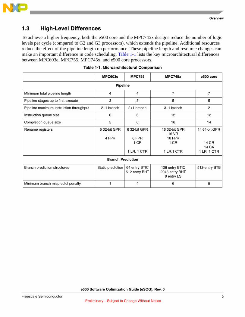


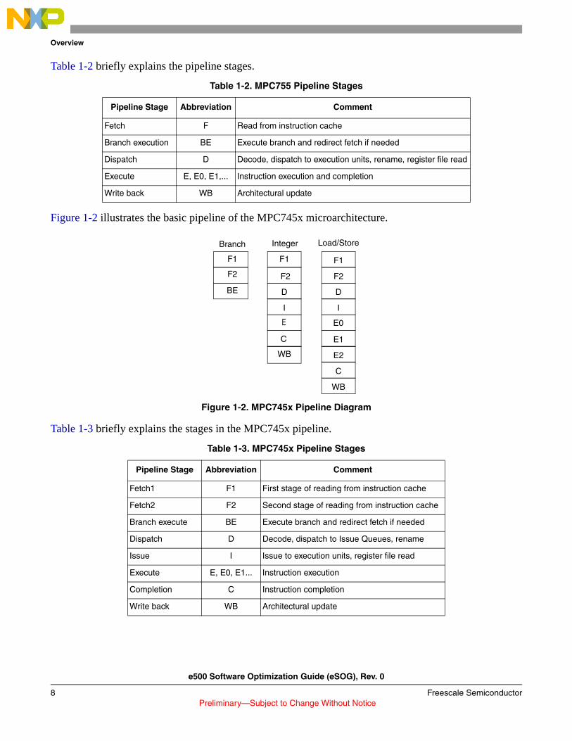
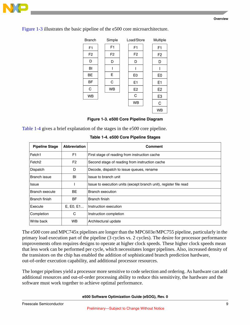

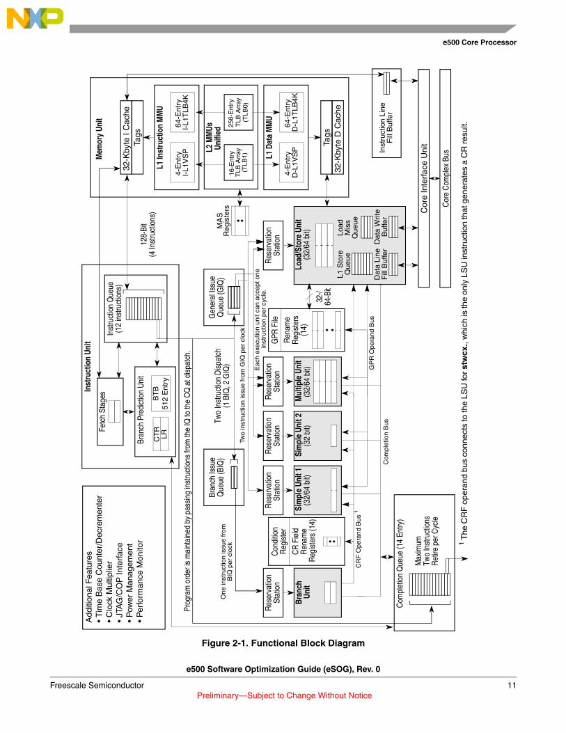


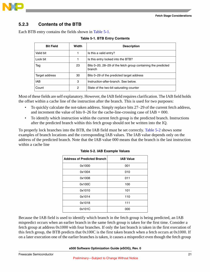
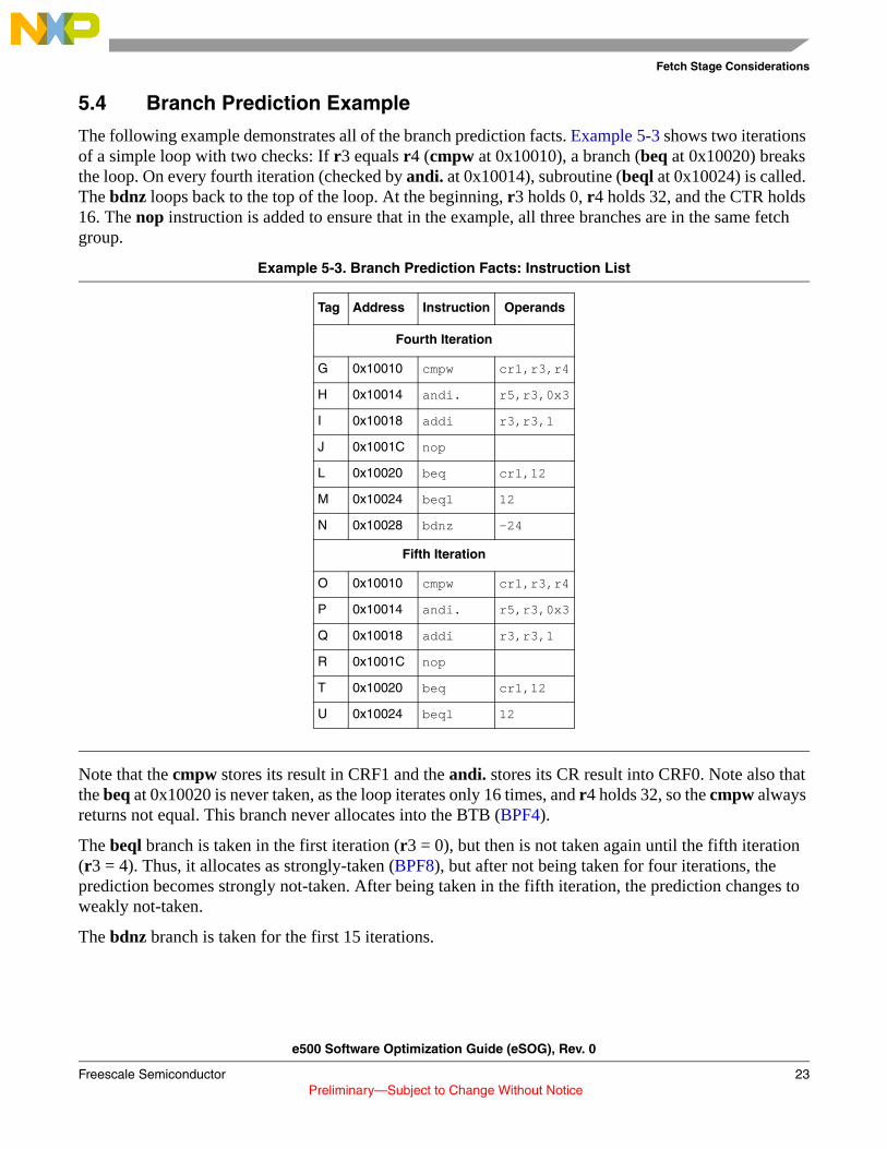
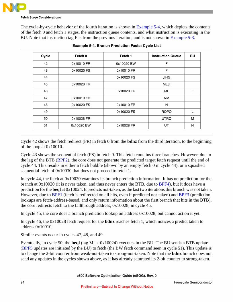

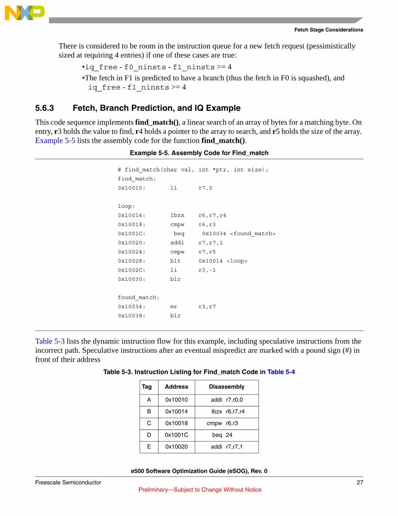
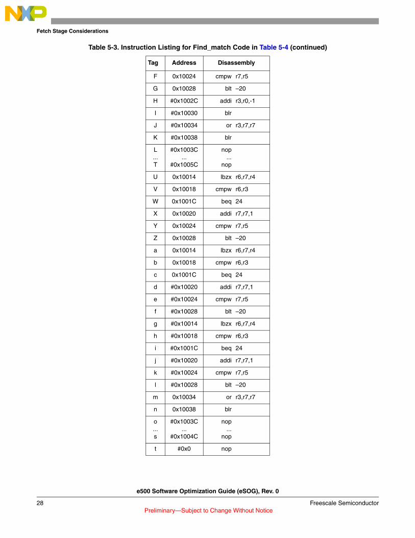


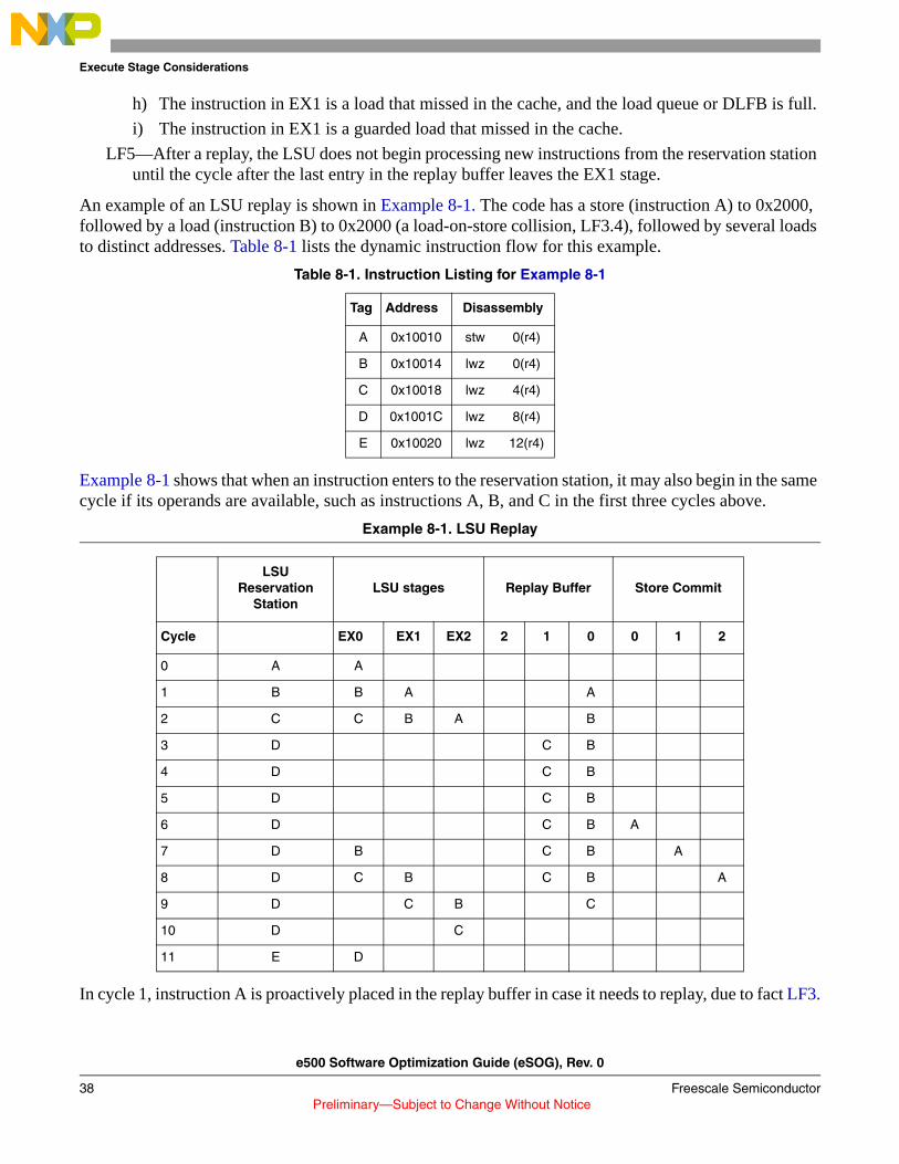
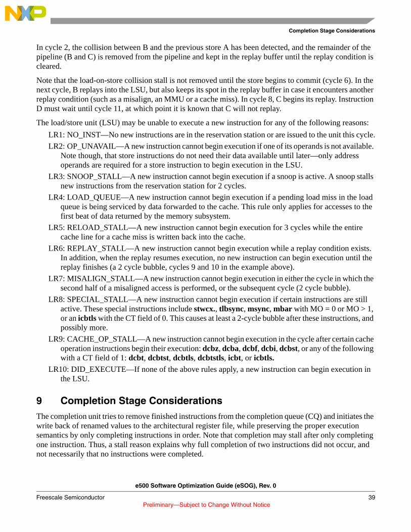


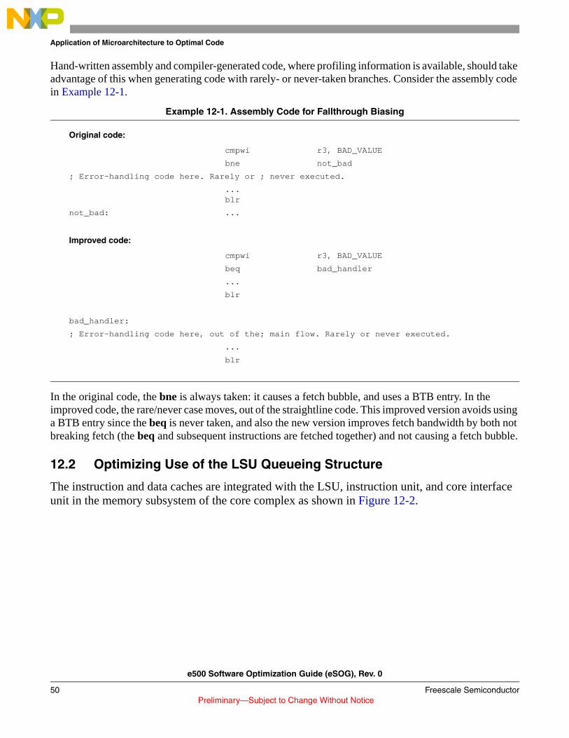


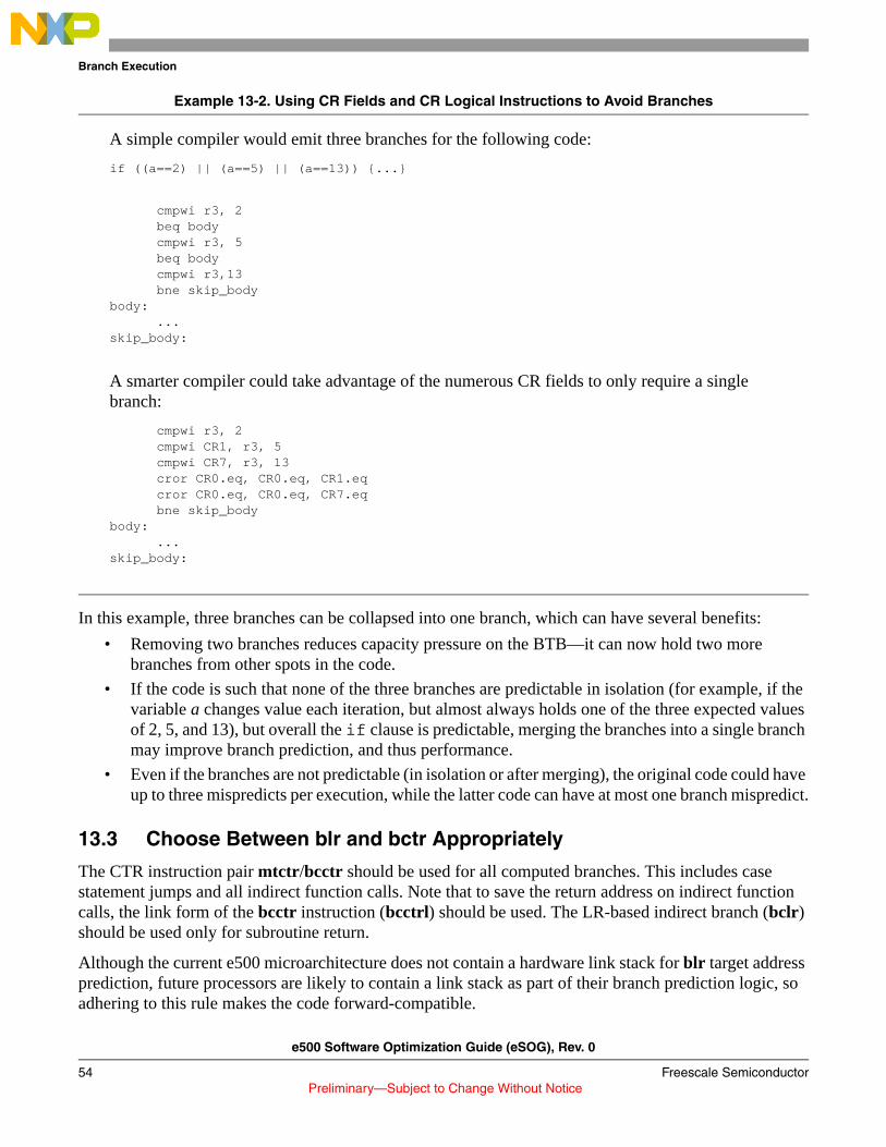
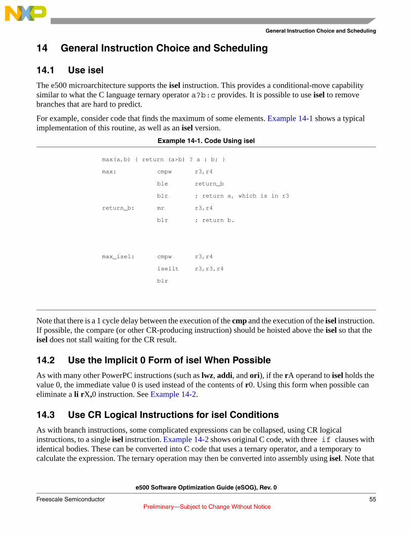


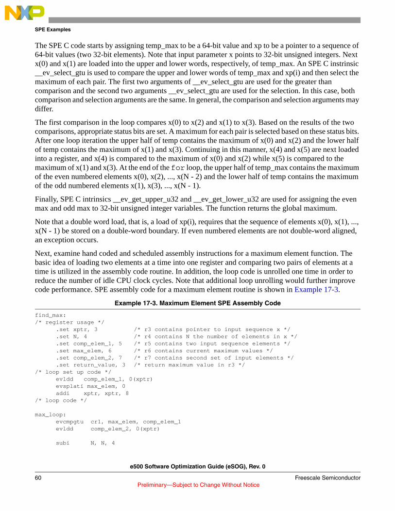


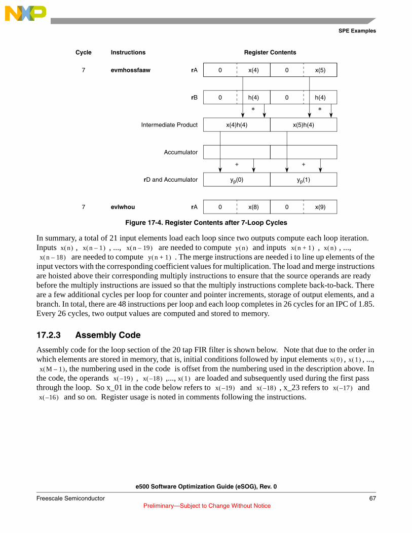


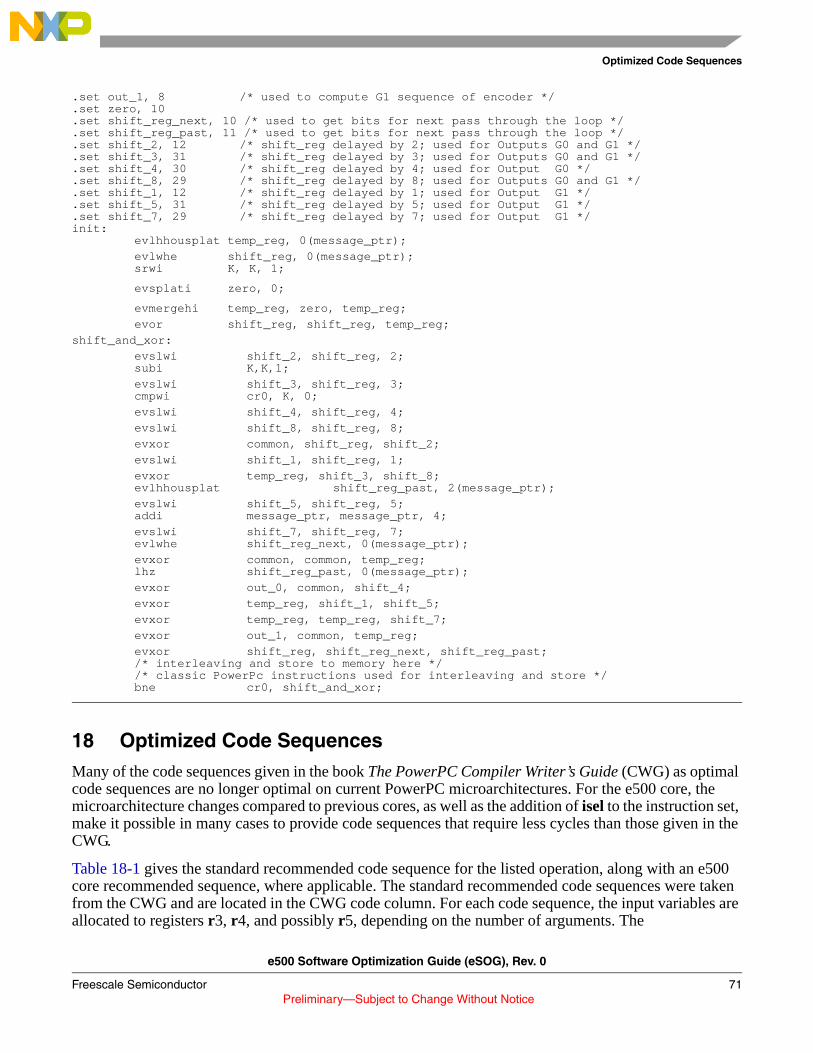

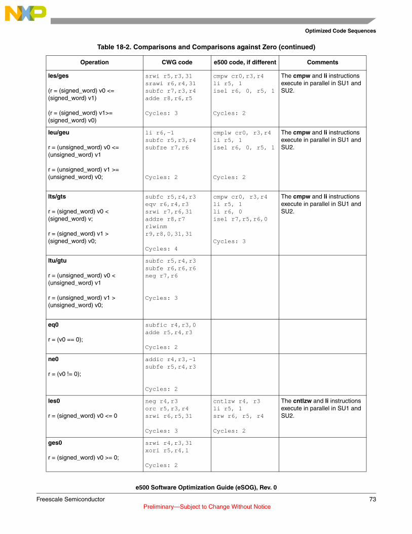
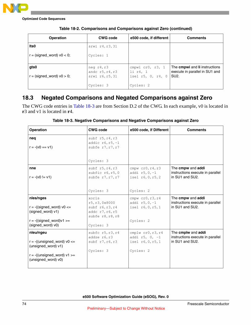


![Compaq Armada E500 V300[1]](https://static.documents.pub/doc/80x56/577d1f4e1a28ab4e1e90511a/compaq-armada-e500-v3001.jpg)

