105
® ® Process Control and Automation Solutions from Elsag Bailey Group E96-301 Universal Analog Input Slave Module (IMASI03)

®®
E96-301
Universal Analog Input Slave Module(IMASI03)
Process Control andAutomation Solutionsfrom Elsag Bailey Group
WARNING notices as used in this instruction apply to hazards or unsafe practices that could result inpersonal injury or death.
CAUTION notices apply to hazards or unsafe practices that could result in property damage.
NOTES highlight procedures and contain information that assists the operator in understanding theinformation contained in this instruction.
WARNING
INSTRUCTION MANUALSDO NOT INSTALL, MAINTAIN, OR OPERATE THIS EQUIPMENT WITHOUT READING, UNDERSTANDING,AND FOLLOWING THE PROPER Elsag Bailey INSTRUCTIONS AND MANUALS; OTHERWISE, INJURY ORDAMAGE MAY RESULT.
RADIO FREQUENCY INTERFERENCEMOST ELECTRONIC EQUIPMENT IS INFLUENCED BY RADIO FREQUENCY INTERFERENCE (RFI). CAU-TION SHOULD BE EXERCISED WITH REGARD TO THE USE OF PORTABLE COMMUNICATIONS EQUIP-MENT IN THE AREA AROUND SUCH EQUIPMENT. PRUDENT PRACTICE DICTATES THAT SIGNSSHOULD BE POSTED IN THE VICINITY OF THE EQUIPMENT CAUTIONING AGAINST THE USE OF POR-TABLE COMMUNICATIONS EQUIPMENT.
POSSIBLE PROCESS UPSETSMAINTENANCE MUST BE PERFORMED ONLY BY QUALIFIED PERSONNEL AND ONLY AFTER SECURINGEQUIPMENT CONTROLLED BY THIS PRODUCT. ADJUSTING OR REMOVING THIS PRODUCT WHILE IT ISIN THE SYSTEM MAY UPSET THE PROCESS BEING CONTROLLED. SOME PROCESS UPSETS MAYCAUSE INJURY OR DAMAGE.
AVERTISSEMENT
MANUELS D’OPÉRATIONNE PAS METTRE EN PLACE, RÉPARER OU FAIRE FONCTIONNER L’ÉQUIPEMENT SANS AVOIR LU,COMPRIS ET SUIVI LES INSTRUCTIONS RÉGLEMENTAIRES DE Elsag Bailey . TOUTE NÉGLIGENCE ÀCET ÉGARD POURRAIT ÊTRE UNE CAUSE D’ACCIDENT OU DE DÉFAILLANCE DU MATÉRIEL.
PERTURBATIONS PAR FRÉQUENCE RADIOLA PLUPART DES ÉQUIPEMENTS ÉLECTRONIQUES SONT SENSIBLES AUX PERTURBATIONS PARFRÉQUENCE RADIO. DES PRÉCAUTIONS DEVRONT ÊTRE PRISES LORS DE L’UTILISATION DU MATÉ-RIEL DE COMMUNICATION PORTATIF. LA PRUDENCE EXIGE QUE LES PRÉCAUTIONS À PRENDREDANS CE CAS SOIENT SIGNALÉES AUX ENDROITS VOULUS DANS VOTRE USINE.
PERTURBATIONS DU PROCÉDÉL’ENTRETIEN DOIT ÊTRE ASSURÉ PAR UNE PERSONNE QUALIFIÉE EN CONSIDÉRANT L’ASPECTSÉCURITAIRE DES ÉQUIPEMENTS CONTRÔLÉS PAR CE PRODUIT. L’AJUSTEMENT ET/OU L’EXTRAC-TION DE CE PRODUIT PEUT OCCASIONNER DES À-COUPS AU PROCÉDÉ CONTRÔLE LORSQU’IL ESTINSÉRÉ DANS UNE SYSTÈME ACTIF. CES À-COUPS PEUVENT ÉGALEMENT OCCASIONNER DESBLESSURES OU DES DOMMAGES MATÉREILS.
NOTICE
The information contained in this document is subject to change without notice.
Elsag Bailey, its affiliates, employees, and agents, and the authors and contributors to this publication specif-ically disclaim all liabilities and warranties, express and implied (including warranties of merchantability andfitness for a particular purpose), for the accuracy, currency, completeness, and/or reliability of the informationcontained herein and/or for the fitness for any particular use and/or for the performance of any material and/or equipment selected in whole or part with the user of/or in reliance upon information contained herein.Selection of materials and/or equipment is at the sole risk of the user of this publication.
This document contains proprietary information of Elsag Bailey, Elsag Bailey Process Automation, andis issued in strict confidence. Its use, or reproduction for use, for the reverse engineering, developmentor manufacture of hardware or software described herein is prohibited. No part of this document may bephotocopied or reproduced without the prior written consent of Elsag Bailey.

I-E96-301B
Preface
The Universal Analog Input Slave Module (IMASI03) interfacesfield inputs to the multi-function processor module. TheIMASI03 supplies 16 separate process field signals into theINFI 90® Process Management System. These analog inputs areused by the Multi-Function Processor Module (MFP) to monitorand control a process.
Universal analog input slave modules provide an isolated ther-mocouple, millivolt, RTD, and high level analog signal interfacefor the Multi-Function Processor Module with variable ana-log-to-digital conversion resolution up to a maximum of 24bits.
This instruction explains the slave module features, specifica-tions and operation. It details the procedures to set up andinstall an IMASI03 module, and explains status indicators thathelp in system test and diagnosis.
System engineers or technicians using the IMASI03 shouldread and understand this instruction before installing andoperating the slave module. In addition, a complete under-standing of the INFI 90 system is beneficial to the user.
® INFI 90 is a registered trademark of Elsag Bailey Process Automation.
1 15 December 1994
®
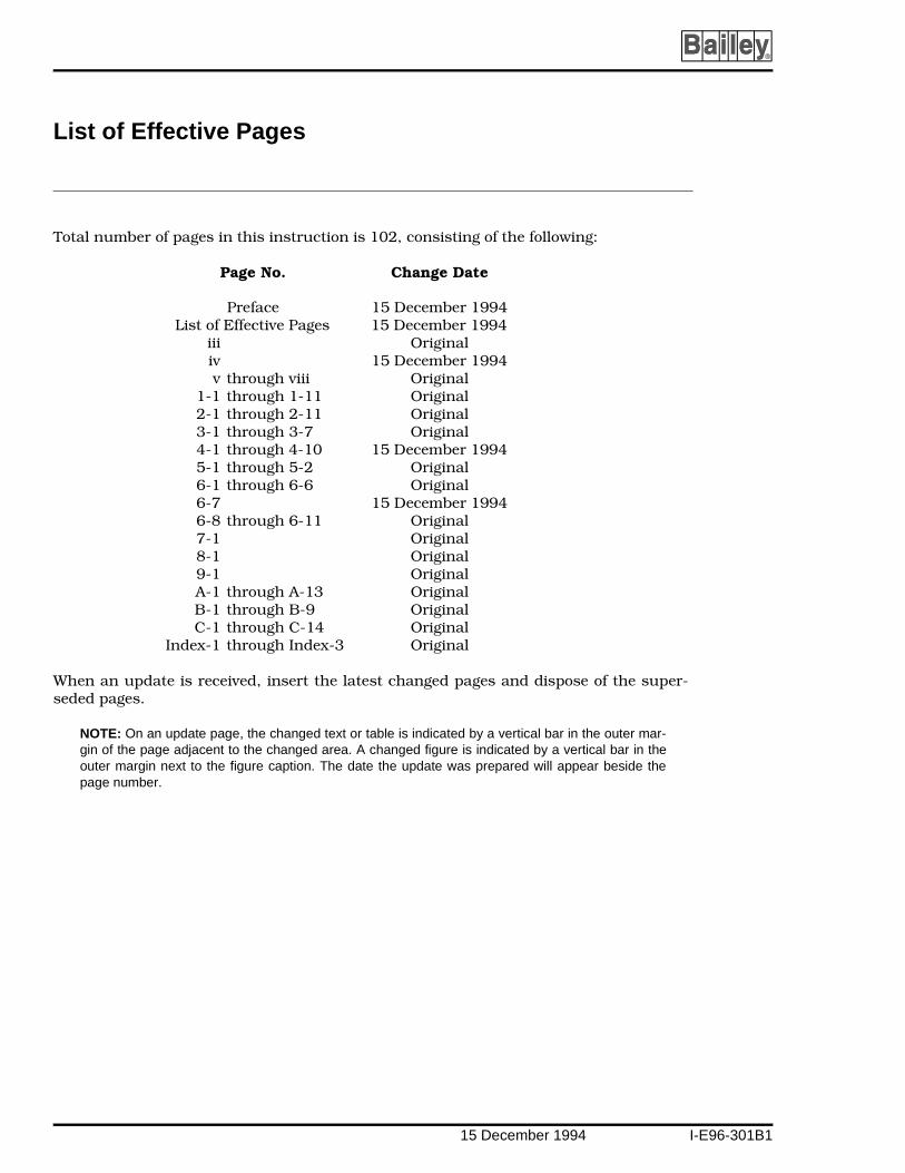
List of Effective Pages
Total number of pages in this instruction is 102, consisting of the following:
Page No. Change Date
Preface 15 December 1994List of Effective Pages 15 December 1994
iii Originaliv 15 December 1994v through viii Original
1-1 through 1-11 Original2-1 through 2-11 Original3-1 through 3-7 Original4-1 through 4-10 15 December 19945-1 through 5-2 Original6-1 through 6-6 Original6-7 15 December 19946-8 through 6-11 Original7-1 Original8-1 Original9-1 OriginalA-1 through A-13 OriginalB-1 through B-9 OriginalC-1 through C-14 Original
Index-1 through Index-3 Original
When an update is received, insert the latest changed pages and dispose of the super-seded pages.
NOTE: On an update page, the changed text or table is indicated by a vertical bar in the outer mar-gin of the page adjacent to the changed area. A changed figure is indicated by a vertical bar in theouter margin next to the figure caption. The date the update was prepared will appear beside thepage number.
15 December 1994 I-E96-301B1

I-E96-301B
Safety Summary
GENERAL WARNINGS
Equipment EnvironmentAll components, whether in transportation, operation or storage,must be in a noncorrosive environment.
Electrical Shock Hazard During MaintenanceDisconnect power or take precautions to insure that contact withenergized parts is avoided when servicing.
Special HandlingThis module uses Electrostatic Sensitive Devices (ESD).
SPECIFICWARNINGS
Disconnect power before installing dipshunts for slave modules onthe MMU backplane (slave expander bus). Failure to do so coulsresult in severe or fatal shock. (p. 3-5)
vii
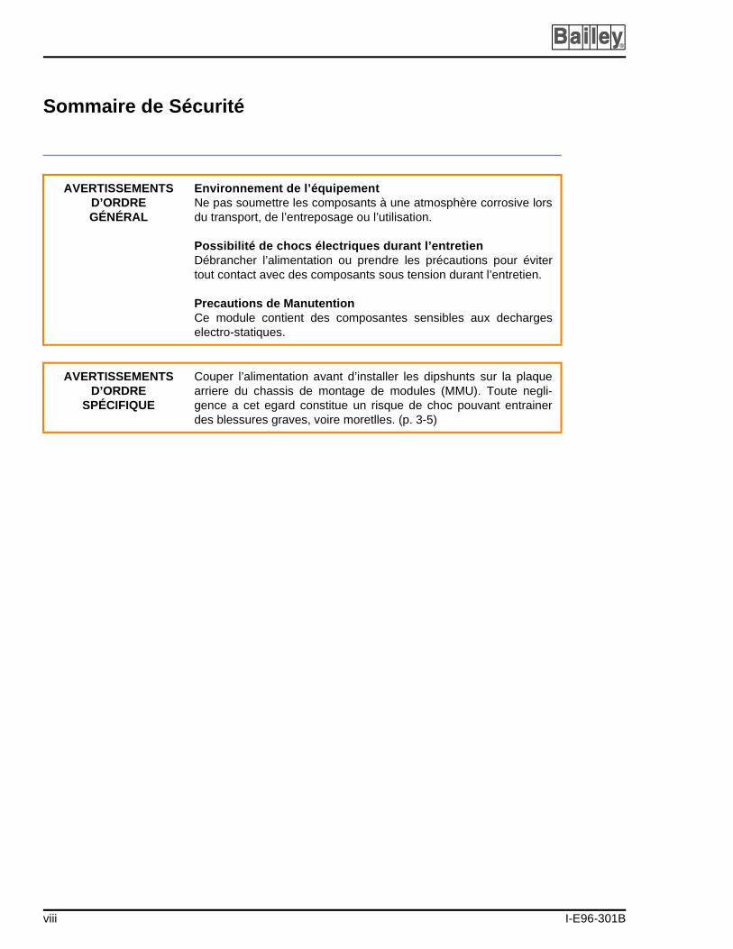
Sommaire de Sécurité
®
AVERTISSEMENTSD’ORDREGÉNÉRAL
Environnement de l’équipementNe pas soumettre les composants à une atmosphère corrosive lorsdu transport, de l’entreposage ou l’utilisation.
Possibilité de chocs électriques durant l’entretienDébrancher l’alimentation ou prendre les précautions pour évitertout contact avec des composants sous tension durant l’entretien.
Precautions de ManutentionCe module contient des composantes sensibles aux dechargeselectro-statiques.
AVERTISSEMENTSD’ORDRE
SPÉCIFIQUE
Couper l’alimentation avant d’installer les dipshunts sur la plaquearriere du chassis de montage de modules (MMU). Toute negli-gence a cet egard constitue un risque de choc pouvant entrainerdes blessures graves, voire moretlles. (p. 3-5)
viii I-E96-301B

Table of Contents
I-E96-301B
Page
SECTION 1 - INTRODUCTION....................................................................................................1-1OVERVIEW ..................................................................................................................1-1INTENDED USER.........................................................................................................1-1MODULE DESCRIPTION ..............................................................................................1-1FEATURES...................................................................................................................1-2INSTRUCTION CONTENT .............................................................................................1-4HOW TO USE THIS MANUAL .......................................................................................1-4GLOSSARY OF TERMS AND ABBREVIATIONS .............................................................1-5REFERENCE DOCUMENTS..........................................................................................1-7NOMENCLATURE ........................................................................................................1-7SPECIFICATIONS.........................................................................................................1-8
SECTION 2 - DESCRIPTION AND OPERATION........................................................................2-1INTRODUCTION...........................................................................................................2-1FUNCTIONAL OPERATION ...........................................................................................2-1BLOCK DIAGRAM ........................................................................................................2-1
Isolation Amplifier..................................................................................................2-2Input Multiplexer (MUX).........................................................................................2-2Analog to Digital Conversion ..................................................................................2-2Microcontroller and Memory ..................................................................................2-3Cold Junction Reference ........................................................................................2-3Switch Settings ......................................................................................................2-4On-Board Indicators ..............................................................................................2-4
SLAVE EXPANDER BUS...............................................................................................2-4Slave Expander Bus Interface ................................................................................2-5Data Values ...........................................................................................................2-5Termination Units..................................................................................................2-5Function Codes......................................................................................................2-5
AUTOMATIC ADJUSTMENTS AND CORRECTIONS.......................................................2-6Input Processing ....................................................................................................2-6Point Value Calculation..........................................................................................2-6Input Calibration ...................................................................................................2-7Lead Wire Resistance Adjustment ..........................................................................2-7Cold Junction Compensation .................................................................................2-7User Gain and Offset Adjustment ...........................................................................2-8Engineering Units Conversion ................................................................................2-8Automatic Calibration ............................................................................................2-9Field Calibration ....................................................................................................2-9
INPUT CALIBRATION ...................................................................................................2-9SECURITY AND INTEGRITY CHECKS...........................................................................2-9
Diagnostics Run on Reset ......................................................................................2-9Diagnostics Run in Diagnostic Mode ....................................................................2-10Diagnostics Run During Normal Operation ..........................................................2-10Expander Bus Communication Security ...............................................................2-10Open Input Detection...........................................................................................2-10Alarm and Exception Reporting ............................................................................2-10
ON-LINE CONFIGURATION ........................................................................................2-11LOGIC POWER...........................................................................................................2-11
iii
Table of Contents (continued)
®
Page
SECTION 3 - INSTALLATION.....................................................................................................3-1INTRODUCTION .......................................................................................................... 3-1SPECIAL HANDLING.................................................................................................... 3-1UNPACKING AND INSPECTION.................................................................................... 3-1SETUP/INSTALLATION................................................................................................ 3-2
Address Selection Switch (SW1) ............................................................................. 3-2Configuring Inputs ................................................................................................ 3-3Termination Module/Unit Configuration ................................................................ 3-5Physical Installation .............................................................................................. 3-5
WIRING CONNECTIONS AND CABLING ....................................................................... 3-5Wiring ................................................................................................................... 3-6Cable Connections................................................................................................. 3-6
SECTION 4 - CONFIGURATION AND CALIBRATION ..............................................................4-1INTRODUCTION .......................................................................................................... 4-1CONFIGURING INPUTS ............................................................................................... 4-1CONFIGURING FUNCTION CODES.............................................................................. 4-1CALIBRATING INPUTS................................................................................................. 4-2FIELD CALIBRATION................................................................................................... 4-3
Field Calibration Instruction.................................................................................. 4-6Test Equipment Required ...................................................................................... 4-6Individual Channel Calibration .............................................................................. 4-7
SECTION 5 - OPERATING PROCEDURES................................................................................5-1INTRODUCTION .......................................................................................................... 5-1START-UP.................................................................................................................... 5-1OPERATION................................................................................................................. 5-1ON-BOARD INDICATORS............................................................................................. 5-1
SECTION 6 - TROUBLESHOOTING...........................................................................................6-1INTRODUCTION .......................................................................................................... 6-1ON-BOARD INDICATORS............................................................................................. 6-1ALARM AND EXCEPTION REPORTING ........................................................................ 6-1PROBLEM REPORTS ................................................................................................... 6-1ERROR MESSAGES AND CORRECTIVE ACTIONS ....................................................... 6-4
Input Channel Status ............................................................................................ 6-4Slave Errors .......................................................................................................... 6-4Error Example ....................................................................................................... 6-6
MODULE FUNCTIONAL TESTS .................................................................................... 6-6Test Equipment Requirements............................................................................... 6-6Switch SW1 Settings.............................................................................................. 6-7
Halt - Display Error......................................................................................... 6-7Continue - Do Not Display Error ...................................................................... 6-8
Dipswitch Configurable Diagnostics....................................................................... 6-8Test Procedure ...................................................................................................... 6-8
Dipswitch Test ................................................................................................ 6-8All Tests Mode................................................................................................. 6-9
Slave Expander Bus Interface Test......................................................................... 6-9Test Procedure ...................................................................................................... 6-9
MODULE PIN CONNECTIONS.................................................................................... 6-10
iv I-E96-301BI-E96-301B115 December 1994
I-E96-301B
Table of Contents (continued)
Page
SECTION 7 - MAINTENANCE.....................................................................................................7-1INTRODUCTION...........................................................................................................7-1MAINTENANCE SCHEDULE.........................................................................................7-1
SECTION 8 - REPAIR/REPLACEMENT PROCEDURES ...........................................................8-1INTRODUCTION...........................................................................................................8-1MODULE REPAIR/REPLACEMENT ..............................................................................8-1
SECTION 9 - SUPPORT SERVICES...........................................................................................9-1INTRODUCTION...........................................................................................................9-1REPLACEMENT PARTS AND ORDERING INFORMATION ..............................................9-1TRAINING ....................................................................................................................9-1TECHNICAL DOCUMENTATION ...................................................................................9-1
APPENDIX A - NIAI05 TERMINATION MODULE CONFIGURATION ...................................... A-1INTRODUCTION.......................................................................................................... A-1
Setup.................................................................................................................... A-1Cold Junction Reference Input .............................................................................. A-1Configuring Inputs................................................................................................ A-2
CONFIGURING INPUTS ............................................................................................... A-4
APPENDIX B - NTAI06 TERMINATION UNIT CONFIGURATION ............................................ B-1INTRODUCTION.......................................................................................................... B-1
Cold Junction Reference Input .............................................................................. B-1Configuring Inputs................................................................................................ B-1
CONFIGURING INPUTS ............................................................................................... B-3
APPENDIX C - FUNCTION CODE DEFINITIONS...................................................................... C-1INTRODUCTION.......................................................................................................... C-1ENHANCED ANALOG SLAVE DEFINITION FUNCTION CODE (FC 215) ........................ C-1ENHANCED ANALOG INPUT DEFINITION FUNCTION CODE (FC 216) ......................... C-5ENHANCED CALIBRATION COMMAND FUNCTION CODE (FC 217) ............................. C-9
List of Tables
No. Title Page
3-1. Address Switch Settings (S1) ..................................................................................3-33-2. IMASI03 Jumper Configurations ............................................................................3-43-3. IMASI03 Jumpers Used for Each Channel ..............................................................3-46-1. IMASI03 Error Types..............................................................................................6-26-2. Module Status (Byte 3) Error Codes .......................................................................6-46-3. Switch SW1 Settings, Operating Modes and Error Messages ...................................6-76-4. P1 Power Pin Connections....................................................................................6-106-5. P2 Expander Bus Connections .............................................................................6-106-6. P3 Input Signal Pin Connections ..........................................................................6-117-1. Maintenance Schedule ...........................................................................................7-1A-1. NIAI05 Input Types ............................................................................................... A-2
v

List of Tables (continued)
No. Title Page
®
A-2. NIAI05 Jumper Configurations ..............................................................................A-2A-3. NIAI05 Input Type Descriptions .............................................................................A-3B-1. NTAI06 Input Types...............................................................................................B-2B-2. NTAI06 Jumper Configurations .............................................................................B-2B-3. NTAI06 Input Type Descriptions ............................................................................B-2C-1. FC 215 Outputs ....................................................................................................C-2C-2. FC 215 Output Descriptions ..................................................................................C-2C-3. FC 215 Specifications ............................................................................................C-2C-4. FC 216 Outputs ....................................................................................................C-5C-5. FC 216 Output Descriptions ..................................................................................C-5C-6. FC 216 Specifications ............................................................................................C-6C-7. FC 216 Input Signal Types ....................................................................................C-7C-8. FC 216 Resolution and Scan Time .........................................................................C-9C-9. FC 217 Outputs ..................................................................................................C-10C-10. FC 217 Output Descriptions ................................................................................C-11C-11. FC 217 Specifications ..........................................................................................C-12
List of Figures
No. Title Page
1-1. INFI 90 Communication Levels .............................................................................. 1-22-1. IMASI03 Functional Block Diagram ....................................................................... 2-23-1. Address Select Switch (SW1).................................................................................. 3-23-2. IMASI03 Jumper Locations.................................................................................... 3-43-3. NIAI05 to IMASI03 Cable Connections ................................................................... 3-63-4. NTAI06 to IMASI03 Cable Connections .................................................................. 3-7A-1. Jumper Locations for Revision A Hardware NIAI05 ................................................A-5A-2. Jumper Locations for Revision B Hardware NIAI05 ................................................A-6A-3. Terminal Assignments for Revision A Hardware NIAI05 ..........................................A-7A-4. Terminal Assignments for Revision B Hardware NIAI05..........................................A-7A-5. Typical Input Circuit for Revision A Hardware........................................................A-8A-6. Typical Input Circuit for Revision B Hardware .......................................................A-9A-7. Field Input Termination Examples for Revision A Hardware NIAI05 ......................A-10A-8. Field Input Termination Examples for Revision B Hardware NIAI05 .....................A-10A-9. Revision A Hardware IMASI03 Input Examples ....................................................A-11A-10. Revision B Hardware IMASI03 Input Examples ....................................................A-12A-11. Cable Connections for Revision A and B Hardware NIAI05 ...................................A-13B-1. Jumper locations and Terminal Assignments for Revision A Hardware NTAI06 ......B-4B-2. Jumper Locations and Terminal Assignments for Revision B Hardware NTAI06 .....B-5B-3. Typical Input Circuit for NTAI06 ............................................................................B-6B-4. Field Input Termination Examples for Revision A and B Hardware NTAI06 .............B-7B-5. IMASI03 Input Examples .......................................................................................B-8B-6. Cable Connections for NTAI06 ...............................................................................B-9C-1. Local Cold Junction Compensation........................................................................C-3C-2. Remote Cold Junction Compensation ....................................................................C-4
vi I-E96-301Bvi I-E96-301B

SECTION 1 - INTRODUCTION
I-E96-301B
OVERVIEW
The Universal Analog Input Slave Module (IMASI03) performsanalog input signal processing for up to 16 input channels andsends this information to a Multi-Function Processor(IMMFP01/02/03) in the INFI 90® System.
This manual explains the purpose, operation, maintenance,handling precautions and installation procedures of the slavemodule.
INTENDED USER
System engineers and technicians should read this manualbefore installing the IMASI03 module. Put the module intooperation only after reading and understanding the informa-tion in this manual. Refer to the Table of Contents to find spe-cific information. Refer to the HOW TO USE THIS MANUALentry in this section to get started.
MODULE DESCRIPTION
The IMASI03 is a single printed circuit board that occupies oneslot in an INFI 90 Module Mounting Unit (MMU). Two captivelatches on the module faceplate secure it to the MMU. Theslave module has three card edge connectors for external sig-nals and power: P1, P2 and P3. P1 connects to the supply volt-ages. P2 connects the IMASI03 to the slave expander bus, overwhich it communicates with the MFP.
Connector P3 carries the inputs from the input cable pluggedinto the termination unit (TU) or termination modules (TM).The terminal blocks for field wiring are on the TU/TM.
The single dipswitch on the IMASI03 module sets the addressfor the slave or selects on-board tests. Refer to Section 3 for thesteps to set the module address. Refer to Section 6 for theon-board tests. Be sure to check the switch setting before put-ting the module into the MMU.
Jumpers configure the type of analog input signals. Refer toSection 3 for the correct setting of these jumpers.
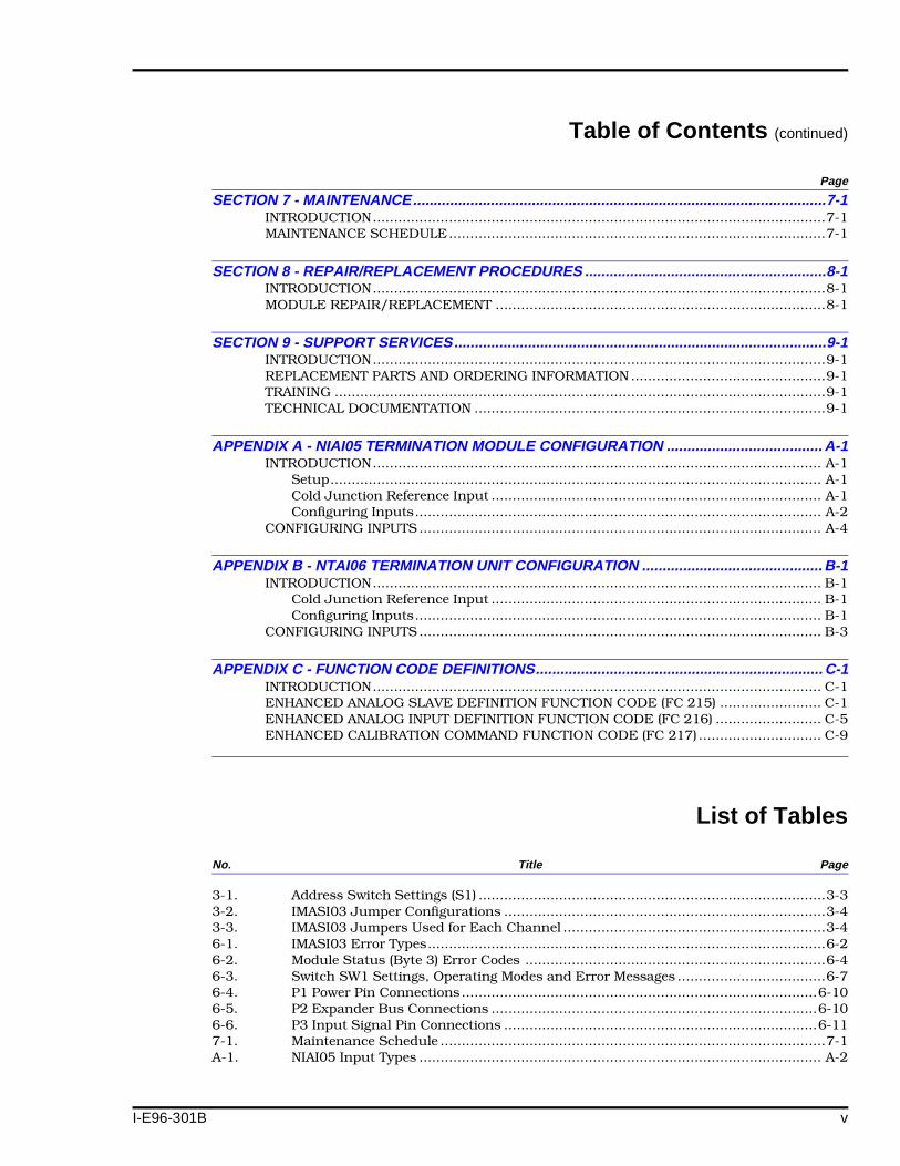
Figure 1-1 shows the INFI 90 communication levels.
® INFI 90 is a registered trademark of Elsag Bailey Process Automation.
OVERVIEW
1 - 1
INTRODUCTION ®
FEATURES
The design of the IMASI03 module, as with all INFI 90 mod-ules, allows for flexibility in creating a process managementsystem. Refer to the NOMENCLATURE entry of this section tosee the list of devices that can be used with the slave module inan INFI 90 system.
• The IMASI03 conditions (filters, amplifies and isolates) upto 16 analog input signals.
• The IMASI03 converts analog signals to digital values, addscompensation and corrections as needed, and provides dig-ital values to the MFP through the slave expander bus.
Figure 1-1. INFI 90 Communication Levels
COMMUNICATION HIGHWAY (INFI-NET OR PLANT LOOP)
CONTROLWAY
MFP
OTHER MODULES
SLAVE EXPANDER BUS
COMMUNICATIONMODULES
TP35388A
IMASI03
TERMINATIONUNIT
NTAI06
ANALOGINPUTS
IMASI03
TERMINATIONMODULE
NIAI05
TERMINATIONMODULE
NIAI05
ANALOGINPUTS
ANALOGINPUTS
OTHER SLAVES NKAS01/11NKAS02/12
FEATURES
1 - 2 I-E96-301B

INTRODUCTION
I-E96-301B
• Each channel is individually programmable for these inputtypes:
E, J, K, L, N (14 AWG), N (28 AWG), R, S, T, U thermocouples.Chinese type E and Chinese type S thermocouples.Millivolt (-100 to +100 mV).3-wire RTDs (10, 100 U.S., 100 European, 120 and Chinese53 Ohm).High level (-10 to +10 V).Current (4-20 mA).
• Resolution of the analog-to-digital conversion process isprogrammable over a range from 16 to 24 bits.
• Input type and channel resolution may be selected inde-pendently for each channel, permitting any mix of inputson a single IMASI03 module.
• Channel isolation and open input detection are providedfor each channel.
• Input circuit offset, gain and nonlinearity errors arerecorded during a one time factory calibration procedure.These measurements provide error compensation duringnormal operation. The slave does automatic recalibrationduring normal operation to compensate for componentaging and temperature drift. No user calibration is everrequired.
• Engineering units conversion to degrees C or F is automat-ically calculated on all input signals that are thermocoupleor RTD types. These conversions correct for nonlinearitiesin the conversion to temperature units using industrystandard linearization tables.
• The slave scales the block output value to engineeringunits for low and high level voltage inputs. Input type andzero and span values are specified in function code 216.
• Thermocouple inputs have cold junction compensation.Each termination device has a built-in cold junction refer-ence. The cold junction reference applied to thermocoupleinputs may be this built-in reference or it may be a remotereference read from another input from this or anotherslave.
• The slave compensates for lead wire resistance in the con-nection between the thermocouple, RTD or low level voltageinput signals.
• The IMASI03 can be removed or installed without turningoff power to the system.
FEATURES
1 - 3
INTRODUCTION ®
INSTRUCTION CONTENT
This manual has nine sections and three appendices.
Introduction Is an overview of the IMASI03 module: features, descriptionand specifications.
Description andOperation
Explains the module operation and input circuits.
Installation Contains the cautions to observe when handling IMASI03 mod-ules. It shows the steps to install and connect the modulebefore applying power. This section also covers switch andjumper settings.
Configuration andCalibration
Presents steps to configure slave inputs for specific input typesand how to field calibrate an input channel for a specific inputtype.
Operating Procedures Explains the operator interface to the IMASI03.
Troubleshooting Describes the IMASI03 error codes and explains how to test theIMASI03.
Maintenance Has a schedule for taking care of the IMASI03. This schedulecan be used for all the modules in the MMU.
Repair/ReplacementProcedures
Contains the cautions and steps for removing and replacingmodules from the MMU.
Support Services Provides a list of information to present when ordering partsfrom the local Bailey Controls sales office. It explains otherareas of support that Bailey Controls provides.
Appendix A Shows the jumper settings, terminal wiring for the NIAI05 ter-mination module and the cabling needed for the IMASI03.
Appendix B Shows the jumper settings, terminal wiring for the NTAI06 ter-mination unit and the cabling needed for the IMASI03.
Appendix C Describes the applications, specifications and block outputsfor function codes 215, 216 and 217.
HOW TO USE THIS MANUAL
Read this manual before handling the IMASI03 module. Referto the sections in this list as needed for more information.
1. Read Section 5 before connecting the IMASI03.
2. Read Section 2.
INSTRUCTION CONTENT
1 - 4 I-E96-301B
INTRODUCTION
I-E96-301B
3. Read and follow the steps in Section 3.
4. Read and follow the configuration steps in Section 4.
5. Refer to Section 6 for what to do if a problem occurs.
6. Refer to Section 7 for the scheduled steps needed to main-tain the IMASI03.
7. Refer to Section 8 for steps to replace a module.
8. Use Section 9 to order parts. This section also explainssome of the many services Bailey offers.
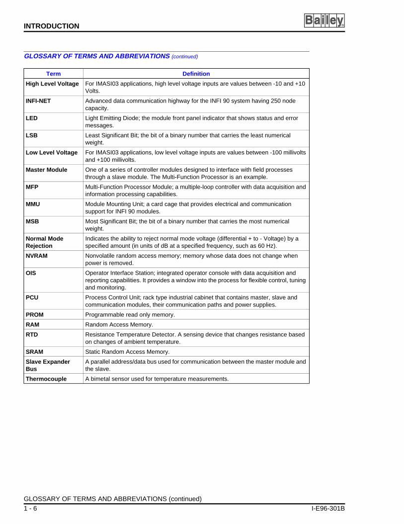
GLOSSARY OF TERMS AND ABBREVIATIONS
Term Definition
A/D Conversion Analog-to-digital conversion; process of generating a digital, (numeric) value representing the magnitude of an analog signal.
Analog Signal A variable input signal that may be any value within a given range.
Cold Junction Reference
The ambient temperature at the bimetal junction of terminated thermocouple wires.
Common Mode Isolation
Indicates the ability to isolate common mode voltages between inputs and outputs and protect a measurement circuit from damage up to a maximum specified voltage level. Also indicates the ability to reject the common mode voltage by a specified amount (in units of dB at a specific frequency, such as 60 Hz).
Configuration A control strategy with function blocks.
Controlway A redundant peer-to-peer communication path for point data transfer between intelligent modules within a process control unit.
Digital Signal A discrete input signal having only ON and OFF states.
Digital Value The representation of a value by some number of digital bits that is capable of being read by a microprocessor.
Dipshunt Dual in-line package with shorting bars.
Dipswitch A dual in-line package that contains single pole switches.
Dual Port RAM (DPRAM)
SRAM shared by two devices. Either device can write or read to the SRAM simultaneously through separate address and data ports.
EWS Engineering Work Station; an integrated hardware and software personal computer system for configuring and monitoring INFI 90 modules and systems.
Function Code (FC) An algorithm that defines specific functions. These functions link together to form the control strategy.
FTP Field Termination Panel.
GLOSSARY OF TERMS AND ABBREVIATIONS
1 - 5
INTRODUCTION ®
GLOSSARY OF TERMS AND ABBREVIATIONS (continued)
Term Definition
High Level Voltage For IMASI03 applications, high level voltage inputs are values between -10 and +10 Volts.
INFI-NET Advanced data communication highway for the INFI 90 system having 250 node capacity.
LED Light Emitting Diode; the module front panel indicator that shows status and error messages.
LSB Least Significant Bit; the bit of a binary number that carries the least numerical weight.
Low Level Voltage For IMASI03 applications, low level voltage inputs are values between -100 millivolts and +100 millivolts.
Master Module One of a series of controller modules designed to interface with field processes through a slave module. The Multi-Function Processor is an example.
MFP Multi-Function Processor Module; a multiple-loop controller with data acquisition and information processing capabilities.
MMU Module Mounting Unit; a card cage that provides electrical and communication support for INFI 90 modules.
MSB Most Significant Bit; the bit of a binary number that carries the most numerical weight.
Normal Mode Rejection
Indicates the ability to reject normal mode voltage (differential + to - Voltage) by a specified amount (in units of dB at a specified frequency, such as 60 Hz).
NVRAM Nonvolatile random access memory; memory whose data does not change when power is removed.
OIS Operator Interface Station; integrated operator console with data acquisition and reporting capabilities. It provides a window into the process for flexible control, tuning and monitoring.
PCU Process Control Unit; rack type industrial cabinet that contains master, slave and communication modules, their communication paths and power supplies.
PROM Programmable read only memory.
RAM Random Access Memory.
RTD Resistance Temperature Detector. A sensing device that changes resistance based on changes of ambient temperature.
SRAM Static Random Access Memory.
Slave Expander Bus
A parallel address/data bus used for communication between the master module and the slave.
Thermocouple A bimetal sensor used for temperature measurements.
GLOSSARY OF TERMS AND ABBREVIATIONS (continued)
1 - 6 I-E96-301B
INTRODUCTION
I-E96-301B
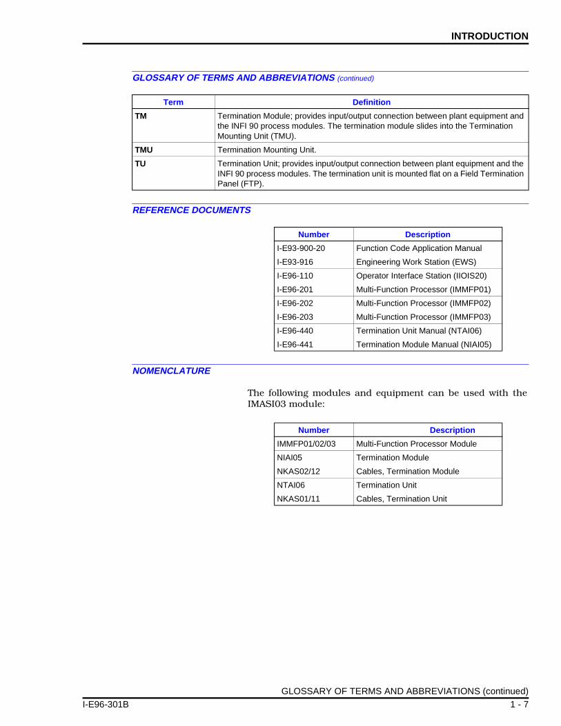
GLOSSARY OF TERMS AND ABBREVIATIONS (continued)
REFERENCE DOCUMENTS
NOMENCLATURE
The following modules and equipment can be used with theIMASI03 module:
Term Definition
TM Termination Module; provides input/output connection between plant equipment and the INFI 90 process modules. The termination module slides into the Termination Mounting Unit (TMU).
TMU Termination Mounting Unit.
TU Termination Unit; provides input/output connection between plant equipment and the INFI 90 process modules. The termination unit is mounted flat on a Field Termination Panel (FTP).
Number Description
I-E93-900-20 Function Code Application Manual
I-E93-916 Engineering Work Station (EWS)
I-E96-110 Operator Interface Station (IIOIS20)
I-E96-201 Multi-Function Processor (IMMFP01)
I-E96-202 Multi-Function Processor (IMMFP02)
I-E96-203 Multi-Function Processor (IMMFP03)
I-E96-440 Termination Unit Manual (NTAI06)
I-E96-441 Termination Module Manual (NIAI05)
Number Description
IMMFP01/02/03 Multi-Function Processor Module
NIAI05 Termination Module
NKAS02/12 Cables, Termination Module
NTAI06 Termination Unit
NKAS01/11 Cables, Termination Unit
GLOSSARY OF TERMS AND ABBREVIATIONS (continued)
1 - 7

INTRODUCTION ®
SPECIFICATIONS
Power Consumption
+ 5 VDC typical 300 mA, maximum 450 mA+ 15 VDC typical 130 mA, maximum 150 mA- 15 VDC typical 35 mA, maximum 50 mA
Analog Input Types
Analog Input Channels 16 independently configured channels
Thermocouples Type E, J, K, L, N (14 AWG), N (28 AWG), R, S, T, UChinese type E and Chinese type S
3-Wire RTD 100 Ohm platinum: U.S. Lab. Standard100 Ohm platinum: U.S. Industry Standard100 Ohm platinum: European Standard 120 Ohm nickel10 Ohm copperChinese 53 Ohm copper
Millivolt -100 mV to +100 mV, o to 100 mV
High Level 1-5 VDC, 0-5 VDC, 0-10 VDC-10 VDC to +10 VDC, or user specified rangewithin -10 VDC and +10 VDC
Current 4-20 mA, system or external powered.
High Level Voltage Analog Accuracy
4-20 mA Current Inputs Add 0.025% to high level voltage analog error values
25o C Ambient Operating TemperaturePower Supplies at Nominal ValuesZero Lead Wire ResistanceFull Scale Range (FSR) = 20.0 V
Resolution Error(Two Standard Deviations From Mean)
Typical Noise(Reading Stability)
Bits ± Percent FSR ± Millivolts ± Percent FSR ± Millivolts
16 0.05 10 0.02 4
18 0.04 8 0.015 3
20 0.03 6 0.0125 2.5
22 0.02 4 0.005 1
24 0.015 3 0.0025 0.5
SPECIFICATIONS
1 - 8 I-E96-301B

INTRODUCTION
I-E96-301B
SPECIFICATIONS (continued)
Low Level Voltage Analog Accuracy
25o C Ambient Operating TemperaturePower Supplies at Nominal ValuesZero Lead Wire ResistanceFull Scale Range (FSR) = 200.0 mV
Resistance Analog Accuracy
25o C Ambient Operating TemperaturePower Supplies at Nominal ValuesZero Lead Wire ResistanceFull Scale Range (FSR) = 500 Ohms
Cold Junction Reference Accuracy
± 0.5° C
Software Temperature Linearization Accuracy
± 0.1° C
Resolution Error(Two Standard Deviations From Mean)
Typical Noise(Reading Stability)
Bits ± Percent FSR ± Millivolts ± Percent FSR ± Millivolts
16 0.05 100 0.03 60
18 0.03 60 0.025 50
20 0.025 50 0.02 40
22 0.025 50 0.015 30
24 0.025 50 0.01 20
Resolution Error(Two Standard Deviations From Mean)
Typical Noise(Reading Stability)
Bits ± Percent FSR ± Ohms ± Percent FSR ± Ohms
16 0.1 0.5 0.06 0.3
18 0.075 0.375 0.06 0.3
20 0.07 0.35 0.03 0.3
22 0.06 0.3 0.03 0.15
24 0.05 0.25 0.03 0.15
SPECIFICATIONS (continued)
1 - 9
INTRODUCTION ®
SPECIFICATIONS (continued)
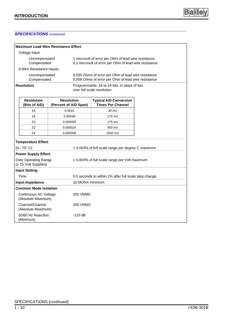
Maximum Lead Wire Resistance Effect
Voltage Input
UncompensatedCompensated
1 microvolt of error per Ohm of lead wire resistance0.1 microvolt of error per Ohm of lead wire resistance
3-Wire Resistance Inputs
UncompensatedCompensated
0.020 Ohms of error per Ohm of lead wire resistance0.008 Ohms of error per Ohm of lead wire resistance
Resolution Programmable, 16 to 24 bits, in steps of two over full scale resolution
Temperature Effect
(0 - 70° C) ± 0.003% of full scale range per degree C maximum
Power Supply Effect
Over Operating Range(± 15 Volt Supplies)
± 0.003% of full scale range per Volt maximum
Input Setting
Time 0.5 seconds to within 1% after full scale step change
Input Impedance 10 MOhm minimum
Common Mode Isolation
Continuous AC Voltage (Absolute Maximum)
250 VRMS
Channel/Channel(Absolute Maximum)
250 VRMS
50/60 Hz Rejection(Minimum)
-110 dB
Resolution (Bits of A/D)
Resolution (Percent of A/D Span)
Typical A/D Conversion Times Per Channel
16 0.0015 30 ms
18 0.00038 175 ms
20 0.000095 175 ms
22 0.000024 450 ms
24 0.000006 2000 ms
SPECIFICATIONS (continued)
1 - 10 I-E96-301B

INTRODUCTION
I-E96-301B
SPECIFICATIONS (continued)
Normal Mode Rejection
Peak or Continuous Voltage(Absolute Maximum)
± 15 VDC
50/60 Hz AC Rejection(Minimum)
-80 dB
Environment
Electromagnetic No values available at this time.
Radio FrequencyInterference
Keep cabinet doors closed. Do not use communication equipment closer than 2 meters from the cabinet.
Ambient Temperature 0 to 70o C (32 to 158o F)
Relative Humidity 5% to 95% up to 55o C (131o F) (noncondensing)5% to 45% at 70o C (158o F) (noncondensing)
Atmospheric Pressure Sea level to 3 km (1.86 miles)(86 kPa to 108 kPa)
Air Quality Noncorrosive
Mounting Occupies a single slot in a standard INFI 90 Module Mounting Unit (MMU).
Shipping Weight 1.146 kg (2.5 lb)
Container Size 27.94 cm x 35.56 cm x 5.54 cm (11 in. x 14 in. x 3 in.)
Certification CSA certified for use as process control equipment in an ordinary (nonhazardous) location.
Complies with IEEE-472 Surge withstand test. NOTE: Absolute maximum ratings indicate limits beyond which damage to the device may occur and device operation is not guaranteed.
Specifications are subject to change without notice.
SPECIFICATIONS (continued)
1 - 11
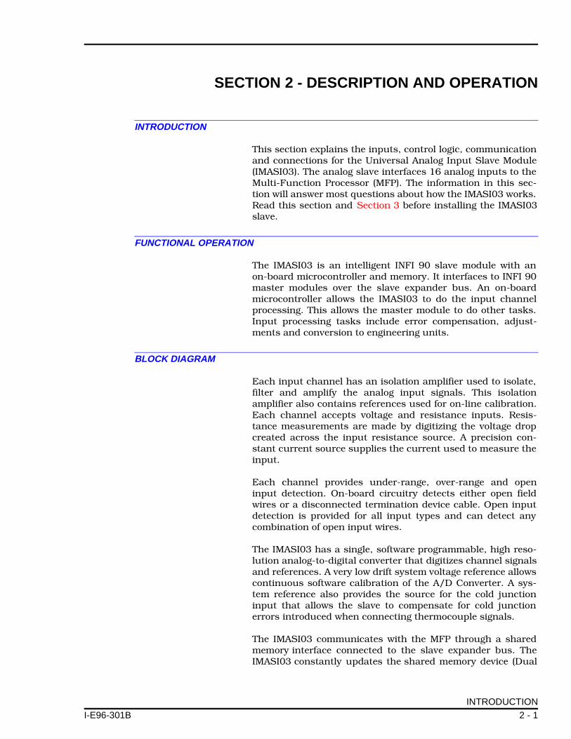
SECTION 2 - DESCRIPTION AND OPERATION
I-E96-301B
INTRODUCTION
This section explains the inputs, control logic, communicationand connections for the Universal Analog Input Slave Module(IMASI03). The analog slave interfaces 16 analog inputs to theMulti-Function Processor (MFP). The information in this sec-tion will answer most questions about how the IMASI03 works.Read this section and Section 3 before installing the IMASI03slave.
FUNCTIONAL OPERATION
The IMASI03 is an intelligent INFI 90 slave module with anon-board microcontroller and memory. It interfaces to INFI 90master modules over the slave expander bus. An on-boardmicrocontroller allows the IMASI03 to do the input channelprocessing. This allows the master module to do other tasks.Input processing tasks include error compensation, adjust-ments and conversion to engineering units.
BLOCK DIAGRAM
Each input channel has an isolation amplifier used to isolate,filter and amplify the analog input signals. This isolationamplifier also contains references used for on-line calibration.Each channel accepts voltage and resistance inputs. Resis-tance measurements are made by digitizing the voltage dropcreated across the input resistance source. A precision con-stant current source supplies the current used to measure theinput.
Each channel provides under-range, over-range and openinput detection. On-board circuitry detects either open fieldwires or a disconnected termination device cable. Open inputdetection is provided for all input types and can detect anycombination of open input wires.
The IMASI03 has a single, software programmable, high reso-lution analog-to-digital converter that digitizes channel signalsand references. A very low drift system voltage reference allowscontinuous software calibration of the A/D Converter. A sys-tem reference also provides the source for the cold junctioninput that allows the slave to compensate for cold junctionerrors introduced when connecting thermocouple signals.
The IMASI03 communicates with the MFP through a sharedmemory interface connected to the slave expander bus. TheIMASI03 constantly updates the shared memory device (Dual
INTRODUCTION
2 - 1
DESCRIPTION AND OPERATION ®
TO/FROMMFP
MASTER
TP35252A
Port RAM) with the current values of the inputs. The MFP canread these values at any time, even if the IMASI03 is simulta-neously writing to the dual port RAM.
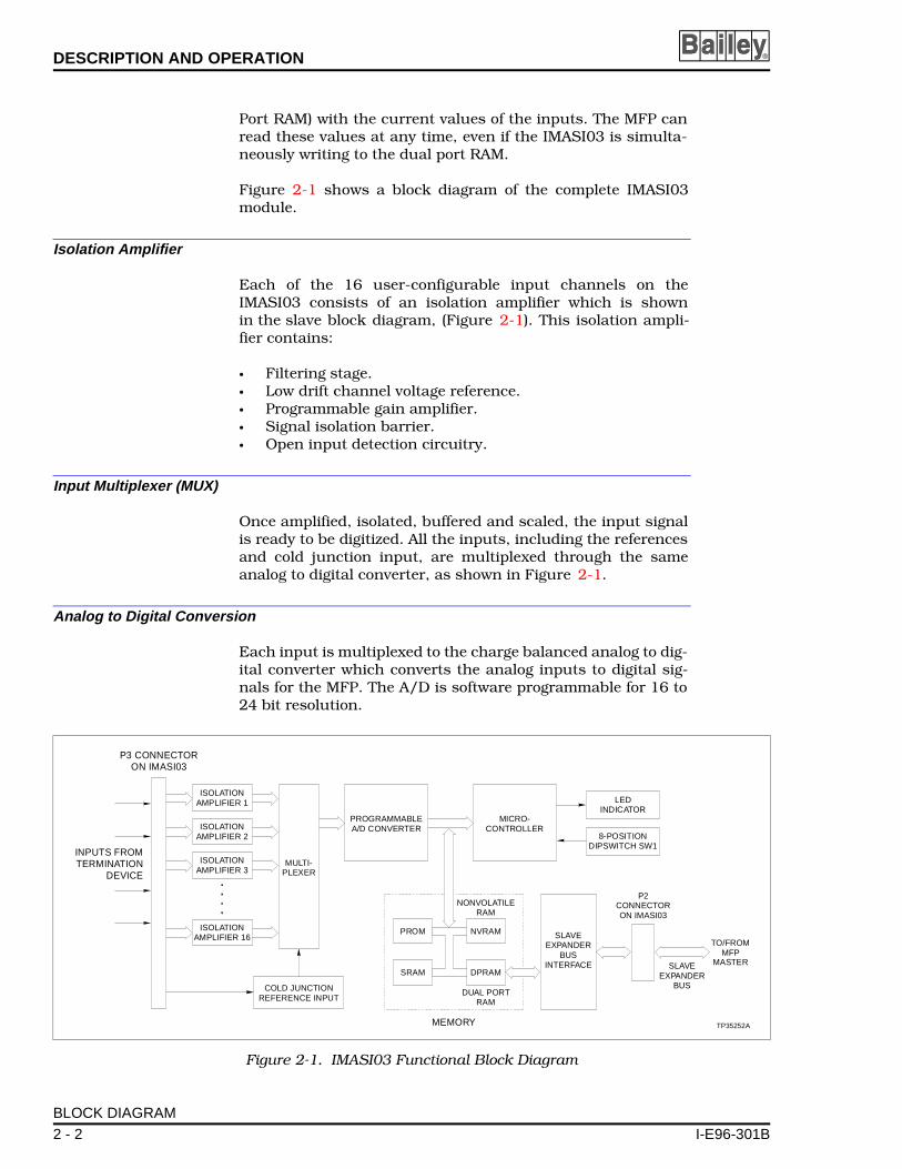
Figure 2-1 shows a block diagram of the complete IMASI03module.
Isolation Amplifier
Each of the 16 user-configurable input channels on theIMASI03 consists of an isolation amplifier which is shownin the slave block diagram, (Figure 2-1). This isolation ampli-fier contains:
• Filtering stage.• Low drift channel voltage reference. • Programmable gain amplifier.• Signal isolation barrier.• Open input detection circuitry.
Input Multiplexer (MUX)
Once amplified, isolated, buffered and scaled, the input signalis ready to be digitized. All the inputs, including the referencesand cold junction input, are multiplexed through the sameanalog to digital converter, as shown in Figure 2-1.
Analog to Digital Conversion
Each input is multiplexed to the charge balanced analog to dig-ital converter which converts the analog inputs to digital sig-nals for the MFP. The A/D is software programmable for 16 to24 bit resolution.
Figure 2-1. IMASI03 Functional Block Diagram
ISOLATIONAMPLIFIER 1
MULTI-PLEXER
PROGRAMMABLEA/D CONVERTER
PROM
SRAM
NVRAM
DUAL PORTRAM
MEMORY
NONVOLATILERAM
DPRAM
MICRO-CONTROLLER
LEDINDICATOR
8-POSITIONDIPSWITCH SW1
COLD JUNCTIONREFERENCE INPUT
ISOLATIONAMPLIFIER 2
ISOLATIONAMPLIFIER 3
ISOLATIONAMPLIFIER 16
P3 CONNECTORON IMASI03
INPUTS FROMTERMINATION
DEVICE
SLAVEEXPANDER
BUSINTERFACE
P2CONNECTORON IMASI03
SLAVEEXPANDER
BUS
BLOCK DIAGRAM
2 - 2 I-E96-301B
DESCRIPTION AND OPERATION
I-E96-301B
Each input channel can be independently configured for reso-lution through individual function code 216 blocks. The reso-lution and approximate conversion speed are shown inAppendix C function code 216.
Microcontroller and Memory
The on-board microcontroller coordinates IMASI03 functions.The main functions are:
• Calibrating the A/D converter.
• Isolation amplifier input reference switching.
• Channel and cold junction reference switching.
• Programming A/D resolution.
• Reading the A/D and applying all necessary correctionfactors.
• Interfacing to switch and LED (used for diagnostic mode).
• Background integrity checks.
• Reads and writes of expander bus data through dual portRAM (DPRAM).
Cold Junction Reference
The IMASI03 measures the cold junction RTDs on the slave'stermination device. This results in an accurate reading of theambient temperature at the field wire termination area. Thisvalue can be used by the slave to compensate for voltages gen-erated from the bimetal connections made by terminating thefield wires (thermocouple wires) onto the terminal blocks of thetermination device.
The block address of the cold junction reference used by ther-mocouple inputs on the slave is contained in function code 215specification 3.
Each slave configured for a thermocouple input requires a coldjunction reference. Each slave can only have one referencewhich can be used by up to 16 thermocouple inputs. Theexception to this is when one of the inputs is used as a remotecold junction reference.
Refer to Section 4 for more information.
BLOCK DIAGRAM
2 - 3

DESCRIPTION AND OPERATION ®
Switch Settings
The IMASI03 has one 8-position DIP switch to select the slaveaddress for the slave expander bus. This switch also selectsbuilt-in diagnostics for a stand-alone test.
On-Board Indicators
The IMASI03 has one red/green LED indicator which showsthe operating status. The LED will:
• Flash red on power-up.
• Remain off after passing on board diagnostics until theIMASI03 is configured by the MFP.
• Show solid green after the master MFP downloads configu-ration data.
• Show solid green during normal running.
• Blink green when the MFP which configured the IMASI03enters configure mode from execute mode.
• Blink green if slave expander bus communication is lost (ifthe MFP is removed).
• Show solid red if a fatal failure of the IMASI03 moduleoccurs. For example, if power up diagnostics fail.
• Show solid red for a power fail interrupt (PFI).
• Show pass/fail of diagnostic routines when in diagnosticmode (refer to Section 6).
SLAVE EXPANDER BUS
The INFI 90 slave expander bus is a high speed synchronousparallel bus. It provides a path between MFP master modulesand slave modules. The master module sends control functionsto the IMASI03, and the IMASI03 provides input data to themaster module. The P2 card edge of the IMASI03 and mastermodule connect to the bus.
The slave expander bus is 12 parallel signal lines located onthe module mounting unit (MMU) backplane. A 12-positiondipshunt placed in a socket on the MMU backplane connectsthe bus between the master and slave modules. Cable assem-blies can extend the bus to eight MMUs.
A master module and its slaves form a subsystem within a Pro-cess Control Unit (PCU). The slave expander bus between mas-ter/slave subsystems must be separated. Leaving a dipshunt
SLAVE EXPANDER BUS
2 - 4 I-E96-301B

DESCRIPTION AND OPERATION
I-E96-301B
socket empty or not connecting the MMUs with cables sepa-rates them.
Slave Expander Bus Interface
The IMASI03 uses a custom gate array for the slave expanderbus interface. An integrated circuit holds all the control logicand communication protocol. This integrated circuit providesthese functions:
• Address comparison and detection.• Message decoding and translation.• Data line filtering of bus signals.• On-board bus drivers.• Expander bus watchdog.
A dual port RAM (DPRAM) stores data that can be accessed atthe same time by the MFP and the slave's microcontroller.
Data Values
For all inputs, channel values are adjusted based on the fac-tory calibration and drift correction data. Thermocouple inputsreceive cold junction reference compensation. Nonlinearity andlead wire resistance adjustments are performed when neces-sary. The IMASI03 slave provides drift-corrected values to theMFP master over the slave expander bus. These values are inengineering units.
The slave sends a status indication to the MFP master for eachinput channel. This status indicates any hardware errors andchannel configuration errors detected by the slave.
Termination Units
The IMASI03 uses one NTAI06 termination unit or two NIAI05termination modules to connect to field signals. An NKAS01/11 cable connects the termination unit to the slave through theP3 connector. An NKAS02/12 cable connects the terminationmodule to the slave through the P3 connector. The terminationdevices contain RTDs used for cold junction compensation ofthermocouple inputs. They also contain the circuitry needed toconvert 4-20 mA field signals into the 1-5 V needed to input tothe slave. The system power supply is protected from short cir-cuits by current limiting resistors on the NIAI05 (hardwarerevision A) and by fuses on the NTAI06 and NIAI05 (hardwarerevision B).
Function Codes
Function codes 215 and 216 in the master MFP configure theIMASI03 and identify the active analog inputs. One functioncode 215 is required for each IMASI03 slave. One function code216 is required for each input channel used on the slave. Thesefunction codes specify the slave expander bus address of the
SLAVE EXPANDER BUS
2 - 5
DESCRIPTION AND OPERATION ®
IMASI03 module and the channel number on the slave moduleconnected to an analog input signal.
The type of the input, and the zero and span in engineeringunits, must also be specified to ensure proper scaling and cor-rections for calibration, cold junction compensation and non-linearity correction.
Add function code 215 and 216 to the master MFP to configurethe IMASI03. Set function code 217 in the master MFP to cali-brate the IMASI03 or to set the user gain and offset values.Refer to the Function Code Application ManualI-E93-900-20 for more information.
AUTOMATIC ADJUSTMENTS AND CORRECTIONS
Input Processing
The IMASI03 slave scans all active inputs at a rate determinedby the requested input channel resolution. A preset conversiontime is determined for the A/D converter depending upon theconfigured input resolution. Conversion time specifies thelength of time required for a single conversion. The input scansfrom one active channel to the next, as fast as the conversiontime allows.
In addition to the active input channels, the built-in cold junc-tion reference, and the reference values for drift correction aredigitized during normal input scanning.
Point Value Calculation
The slave maintains a set of adjustment values for each inputchannel. These values correct for offset, gain and nonlinearityerrors in the input channel. The raw analog-to-digital convertercount value is first adjusted for any drift in the accuracy of theinput channel components. The resulting value is then con-verted to an actual input signal value using the calibrationdata which also adjusts for any nonlinearity in the input chan-nel circuitry. The lead wire resistance is then taken intoaccount and the required adjustment is made.
For thermocouple inputs, an adjustment is made for the coldjunction temperature of the thermocouple. An additional,user-specified adjustment is then applied, if one has beendefined with function code 217. The final corrected input read-ing is then converted to engineering units using either thermo-couple or RTD conversion tables, or the engineering unit zeroand span values specified for the input.
The following sections describe the various types of input valueadjustments.
AUTOMATIC ADJUSTMENTS AND CORRECTIONS
2 - 6 I-E96-301B

DESCRIPTION AND OPERATION
I-E96-301B
Input Calibration
Each input channel is calibrated at the factory. During the cal-ibration procedure, any offset, gain and nonlinearity errors areidentified and required correction factors are calculated andstored in the slave's nonvolatile memory.
These factors are used when the input channel is scanned tocorrect the reading. A calibration adjustment is applied toactive channels and the cold junction reference input.
Periodic reference readings are taken to provide a correction fordrift of input channel components. This drift calibration is per-formed automatically and continually while normal input pro-cessing is maintained.
Lead Wire Resistance Adjustment
All but high level inputs are adjusted for lead wire resistancecoming into the termination device (The effect of lead wireresistance on high level inputs is negligible). This value is sup-plied through a function code specification and is used by theslave module in its input value calculation. The adjustment forlead wire resistance depends upon the input channel circuitryused for a particular input signal type. For millivolt and ther-mocouple inputs, lead wire resistance is equal to the seriesresistance of the + and - leads. For 3-wire RTD inputs, the leadwire resistance specified in function code 216 specification 10is equal to the resistance of any ONE of the three leads. Allthree resistances must be equal for accurate lead wire resis-tance compensation.
The resistance of the cable from the termination module to theslave module is also taken into account when making thisadjustment.
Cold Junction Compensation
Thermocouple input channels are adjusted for cold junctiontemperature. The cold junction reference may be the built-inreference available on the slave's termination device, or may bea value originating from any other function code block outputanywhere in the INFI 90 system. The cold junction referencesupplied by the MFP is assumed to be in degrees C. The slaveconverts this value to millivolts and adds it to the value fromthe analog-to-digital converter.
Thermocouple channels identified to be cold junction referenceinputs (function code 216 specification 4) use the built-in coldjunction reference on the termination device for their coldjunction compensation.
AUTOMATIC ADJUSTMENTS AND CORRECTIONS
2 - 7

DESCRIPTION AND OPERATION ®
User Gain and Offset Adjustment
A user-specified linear adjustment may be applied to the inputsignal before it is converted to engineering units. This gain andoffset is applied to the value obtained after all compensationand correction operations are performed.
User offset and gain compensates input signals for user correc-tions. For example, if a 0 to 10 Volt analog input is 0.1 Voltstoo high, the slave can compensate for this offset by adding anoffset value of -0.1 for this channel and input type.
User gain value is multiplied times Volts for high level inputs,times millivolts for low level inputs and thermocouple inputs,and times Ohms for RTD inputs. The default user gain is avalue of one.
User offset is added to the input signal. Units of offset are spec-ified as Volts for high level inputs, millivolts for low level inputsand Ohms for RTD inputs. The default user offset is a value ofzero. Separate user gain and offset values can be specified foreach input channel and each input type. The user gain and off-set values can be set and reset using function code 217. Oncedefined, user gain and offset values remain in NVRAM and arenot lost when module power is interrupted. For more informa-tion refer to function code 217 in Appendix C.
Engineering Units Conversion
Thermocouple and RTD inputs are converted to the tempera-ture units specified in function code 216, either degrees C or F.Conversion tables representing the voltage (or resistance) totemperature relationship are used for this conversion. Thetable used in performing the conversion depends upon theinput signal type specified.
If the input is identified as either millivolt or high level, thenthe specified engineering unit zero and span values are used toconvert the input reading to a scaled engineering unit value. Ifspecial calculations need to be performed prior to conversion toengineering units (external to function code 215/216 blocks),then the zero and span values specified in the function codeshould be set to represent a standard voltage span for theinput. The slave function code 216 would then output a cor-rected voltage input reading which may be processed in theMFP through a square root, polynomial, or other functionblock followed by a scaling function to provide the value inengineering units.
AUTOMATIC ADJUSTMENTS AND CORRECTIONS
2 - 8 I-E96-301B

DESCRIPTION AND OPERATION
I-E96-301B
Automatic Calibration
Compensation for drift of input channel circuitry is done byperiodic automatic calibration of each channel using on-boardprecision low-drift references. This function is transparent tonormal input channel processing.
Field Calibration
Field calibration is not necessary in normal situations. It ispossible to perform calibration procedures in the field if ultrastable, known, precision references are available. Field calibra-tion data is stored in NVRAM. The complete field calibrationinstruction is in Section 4.
Factory calibration data is stored in a unique NVRAM area. Iffield calibration does not provide the desired results, the fac-tory calibration data can be restored.
Using Function code 217 to change the gain or offset valuesper channel and type can compensate for differences in inputsignal readings. Tuning these parameters can take the place ofa field calibration. Refer to function code 217 specification 1.
INPUT CALIBRATION
Data from the factory calibration is stored on the slave in non-volatile memory. No customer calibration is necessary. If fieldcalibration is desired, use the procedure in Section 4.
SECURITY AND INTEGRITY CHECKS
Diagnostics Run on Reset
The IMASI03 performs built-in tests on power-up and on resetto check the operation of the module. These tests include:
• PROM checksum verification.• NVRAM checksum verification.• DPRAM/SRAM verification.• Processor instruction set tests.• Timer test.
INPUT CALIBRATION
2 - 9
DESCRIPTION AND OPERATION ®
Diagnostics Run in Diagnostic Mode
The IMASI03 performs built-in tests in diagnostic mode tocheck the operation of the module. These tests include:
• Sixteen channel reference checks.• A/D internal reference checks.• Switch test.• Watchdog timer test.• CPU test.• Timer test.• ROM test.• DPRAM test.• NVRAM test.• SRAM test.• System reference checks.• Configured channel reference checks.• Unconfigured channel reference checks.
Diagnostics Run During Normal Operation
During normal operation, the IMASI03 verifies the checksum ofthe PROM and nonvolatile RAM. Watchdog timers safeguardagainst an A/D converter failure which would halt input scan-ning. Input circuits are monitored for open circuits. Any errorsare reported to the master MFP through the slave module sta-tus. Certain failures detected by these diagnostics may resultin halting the slave.
Expander Bus Communication Security
Expander bus message integrity is maintained by checksumcalculations on each transmitted and received message or dataset.
Open Input Detection
The IMASI03 recognizes and reports any open inputs on activechannels by indicating bad quality on these channels.
Alarm and Exception Reporting
No alarm or exception reports are generated by the functioncodes associated with the IMASI03. The values input from theIMASI03 must be fed to a standard exception reporting block.Refer to Section 6 for more information.
SECURITY AND INTEGRITY CHECKS
2 - 10 I-E96-301B

DESCRIPTION AND OPERATION
I-E96-301B
ON-LINE CONFIGURATION
All specifications in function codes 215, 216 and 217 associ-ated with the IMASI03 may be changed during on-line configu-ration. When changes are made to the input channelparameters (function code 216), the channel will hold the lastvalue for a short period, the status remains unchanged duringthis period. This hold time is based on the number of channelsthat were changed during on-line configuration, as well as theresolution specified in the function code 216 blocks for thatchannel. Plan on a hold time of four seconds (worst case) foreach function code 216 changed during on-line configuration.
LOGIC POWER
The IMASI03 receives its power (+5 V, ±15 V) from the MMUbackplane. Power connects through the top 12-pin card edgeconnector (P1) at the back of the IMASI03.
ON-LINE CONFIGURATION
2 - 11

SECTION 3 - INSTALLATION
I-E96-301B
INTRODUCTION
This section explains what to do before putting the UniversalAnalog Input Slave Module (IMASI03) into operation. DO NOTPROCEED with the installation and operation until you read,understand and do the steps in the order in which they appear.
Refer to Appendix A and Appendix B for termination devicewiring instructions. Refer to Section 4 to configure theIMASI03.
SPECIAL HANDLING
NOTE: Always use Bailey's Field Static Kit (P/N 1948385A2 - wriststrap, ground cord assembly, alligator clip) when working with mod-ules. The kit connects a technician and the module to the sameground point to prevent damage to the module by electrostaticdischarge.
This device uses metal oxide semiconductor (MOS) devices thatrequire special precautions during shipping and handling.Static discharge, improper grounding, and careless handlingcan damage these devices. To help reduce the chance of dam-age, follow these procedures:
1. Keep the module in its special antistatic bag until ready toinstall it. Save the antistatic bag for future use.
2. Ground the antistatic bag before opening it.
3. Make sure all devices to which the module connects areproperly grounded before connection.
4. Avoid touching the circuitry when handling the module.
NOTE: Wear the grounding strap from the field static kit whenremoving or installing the module to change switch settings.
UNPACKING AND INSPECTION
These are steps to follow for general handling:
1. Examine the module to make sure that no damage hasoccurred in transit.
2. Notify the nearest Bailey Controls sales/service office ofany damage.
3. File a claim for any damage with the shipping companythat handled the shipment.
INTRODUCTION
3 - 1
INSTALLATION ®
4. Use the original packing material or container to store themodule.
5. Store the module in a place with clean air; free of extremesof temperature and humidity.
SETUP/INSTALLATION
Before applying power to the IMASI03, make these checks:
1. Check that the module address is set correctly.
2. Check that the jumpers on the module are set correctly.
3. Be sure the dipshunts in the MMU's slave expander busare installed correctly.
4. Check that the jumpers on the termination devices are setcorrectly.
5. Verify I/O cabling connections.
6. Verify there is sufficient logic and field power for the mod-ules in the MMU.
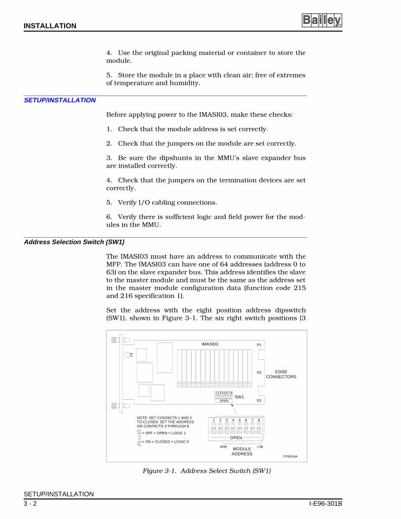
Address Selection Switch (SW1)
The IMASI03 must have an address to communicate with theMFP. The IMASI03 can have one of 64 addresses (address 0 to63) on the slave expander bus. This address identifies the slaveto the master module and must be the same as the address setin the master module configuration data (function code 215and 216 specification 1).
Set the address with the eight position address dipswitch(SW1), shown in Figure 3-1. The six right switch positions (3
Figure 3-1. Address Select Switch (SW1)
IMASI03 P1
P3
P2
TP35254A
SW1OPEN
762 3 4 51 8
1 2 3 4 5 86 7
OPEN
MODULEADDRESS
MSB LSB
NOTE: SET CONTACTS 1 AND 2TO CLOSED. SET THE ADDRESSON CONTACTS 3 THROUGH 8.
= OFF = OPEN = LOGIC 1
= ON = CLOSED = LOGIC 0
EDGECONNECTORS
SETUP/INSTALLATION
3 - 2 I-E96-301B
INSTALLATION
I-E96-301B
through 8) of SW1 set the six bit address. Positions 1 and 2must remain closed (set to zero) for normal operation.
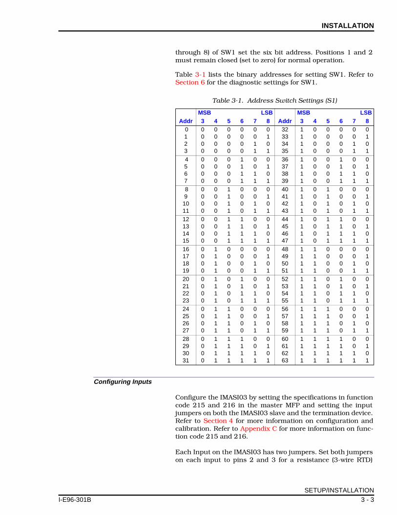
Table 3-1 lists the binary addresses for setting SW1. Refer toSection 6 for the diagnostic settings for SW1.
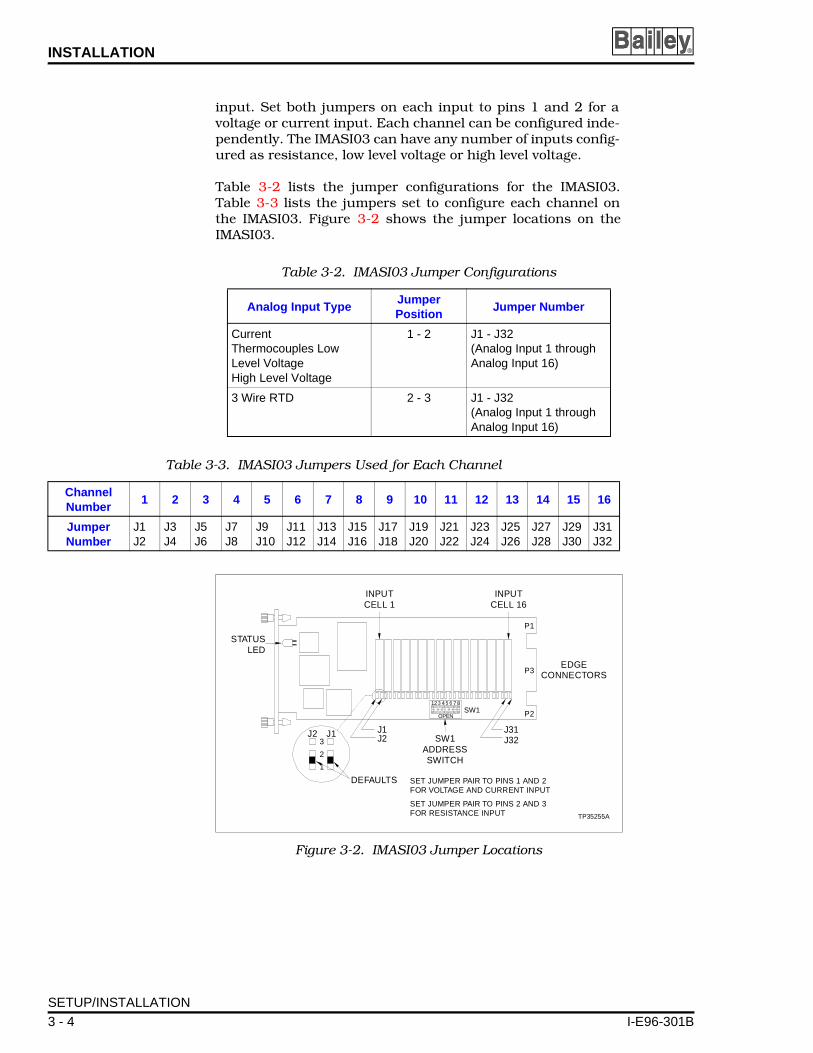
Configuring Inputs
Configure the IMASI03 by setting the specifications in functioncode 215 and 216 in the master MFP and setting the inputjumpers on both the IMASI03 slave and the termination device.Refer to Section 4 for more information on configuration andcalibration. Refer to Appendix C for more information on func-tion code 215 and 216.
Each Input on the IMASI03 has two jumpers. Set both jumperson each input to pins 2 and 3 for a resistance (3-wire RTD)
Table 3-1. Address Switch Settings (S1)
MSB LSB MSB LSBAddr 3 4 5 6 7 8 Addr 3 4 5 6 7 8
0123
0000
0000
0000
0000
0011
0101
32333435
1111
0000
0000
0000
0011
0101
4567
0000
0000
0000
1111
0011
0101
36373839
1111
0000
0000
1111
0011
0101
89
1011
0000
0000
1111
0000
0011
0101
40414243
1111
0000
1111
0000
0011
0101
12131415
0000
0000
1111
1111
0011
0101
44454647
1111
0000
1111
1111
0011
0101
16171819
0000
1111
0000
0000
0011
0101
48495051
1111
1111
0000
0000
0011
0101
20212223
0000
1111
0000
1111
0011
0101
52535455
1111
1111
0000
1111
0011
0101
24252627
0000
1111
1111
0000
0011
0101
56575859
1111
1111
1111
0000
0011
0101
28293031
0000
1111
1111
1111
0011
0101
60616263
1111
1111
1111
1111
0011
0101
SETUP/INSTALLATION
3 - 3
INSTALLATION ®
input. Set both jumpers on each input to pins 1 and 2 for avoltage or current input. Each channel can be configured inde-pendently. The IMASI03 can have any number of inputs config-ured as resistance, low level voltage or high level voltage.
Table 3-2 lists the jumper configurations for the IMASI03.Table 3-3 lists the jumpers set to configure each channel onthe IMASI03. Figure 3-2 shows the jumper locations on theIMASI03.
Table 3-2. IMASI03 Jumper Configurations
Analog Input TypeJumper Position
Jumper Number
Current Thermocouples Low Level VoltageHigh Level Voltage
1 - 2 J1 - J32(Analog Input 1 through Analog Input 16)
3 Wire RTD 2 - 3 J1 - J32(Analog Input 1 through Analog Input 16)
Table 3-3. IMASI03 Jumpers Used for Each Channel
Channel Number
1 2 3 4 5 6 7 8 9 10 11 12 13 14 15 16
Jumper Number
J1J2
J3J4
J5J6
J7J8
J9J10
J11J12
J13J14
J15J16
J17J18
J19J20
J21J22
J23J24
J25J26
J27J28
J29J30
J31J32
Figure 3-2. IMASI03 Jumper Locations
STATUSLED
EDGECONNECTORS
SW1OPEN
762 3 4 51 8
INPUTCELL 1
INPUTCELL 16
P1
P3
P2
J31J1J23
1
2
J32J2J1
DEFAULTS
SW1ADDRESSSWITCH
SET JUMPER PAIR TO PINS 1 AND 2FOR VOLTAGE AND CURRENT INPUT
SET JUMPER PAIR TO PINS 2 AND 3FOR RESISTANCE INPUT TP35255A
SETUP/INSTALLATION
3 - 4 I-E96-301B

INSTALLATION
I-E96-301B
Termination Module/Unit Configuration
Two NIAI05 termination modules or one NTAI06 terminationunit connects the field device wiring to the INFI 90 system. Theterminal blocks are located on the termination device.
Set up the termination device to accept the analog field inputssent to the IMASI03 module. Refer to Appendix A orAppendix B for the termination device for your application.
Physical Installation
NOTE: Section 3 provides data on the physical installation of theslave only. For complete cable and termination module information,refer to Appendix A and Appendix B.
The IMASI03 module occupies one slot in a standard INFI 90Module Mounting Unit (MMU). To install the module:
1. Verify the slot placement of the module.
2. Verify that a dipshunt is in the slave expander bus socketon the MMU backplane between the slave and master module.
3. Connect the hooded end of the cable from the terminationmodule/unit to the MMU backplane. To do this, insert the con-nector into the backplane slot in the same slot as the oneassigned to the slave module. The latches should snap securelyinto place.
4. Align the module with the guide rails in the MMU. Carefullyslide the module in until the front panel is flush with the topand bottom of the MMU frame.
5. Push and turn the two captive latches on the module face-plate one half turn to the latched position. It is latched whenthe slots on the latches are vertical and the open ends face thecenter of the module.
WIRING CONNECTIONS AND CABLING
The IMASI03 has three card edge connectors to supply power(P1), connect slave expander bus communication (P2), and pro-vide analog inputs (P3).
WARNINGDisconnect power before installing dipshunts for slave mod-ules on the MMU backplane (slave expander bus). Failure to doso could result in severe or fatal shock.
AVERTISSEMENTCouper l'alimentation avant d'installer les dipshunts sur laplaque arriere du chassis de montage de modules (MMU).Toute negligence a cet egard constitue un risque de choc pou-vant entrainer des blessures graves, voire moretlles.
WIRING CONNECTIONS AND CABLING
3 - 5

INSTALLATION ®
Wiring
Install the module in the MMU to connect the slave module tothe voltages (+5, ± 15 VDC), needed to power the circuits. TheMMU also connects P2 to the slave expander bus for communi-cation with the master module. P1 and P2 connection requireno additional wiring or cabling.
NOTE: A dipshunt on the backplane of the MMU connects the slaveexpander bus between the slave module and master module.Locate the module so the bus can connect to them or they will notcommunicate.
Cable Connections
The IMASI03 uses two NIAI05 termination modules or oneNTAI06 termination unit for termination.
A single NKAS02 or NKAS12 is used to connect the IMASI03 totwo NIAI05 termination modules. The NTAI06 requires anNKAS01 or NKAS11 to connect to the IMASI03.
The cables have a Y configuration with two connectors on oneend. Note the labeling of J2 and J3 to insure proper connectionof the input signals.
Figure 3-3 shows cable connections to the NIAI05 terminationmodule. Figure 3-4 shows cable connections to the NTAI06 ter-mination unit.
Figure 3-3. NIAI05 to IMASI03 Cable Connections
TP35262A
P1
P3
J2
J3
J1
P2
NKAS02/12(SEE NOTE)
ANALOG SLAVETERMINATION CABLE NIAI05
NIAI05
CHANNELS 1-8ON J2
CHANNELS 9-16ON J3
IMASI03
FIELDWIRING
FIELDWIRING
NOTE: NKAS02 HAS PVC INSULATION (SPECIFY LENGTH UP TO200 FT). NKAS12 HAS NON-PVC INSULATION (SPECIFY LENGTHUP TO 200 FT).
WIRING CONNECTIONS AND CABLING
3 - 6 I-E96-301B

INSTALLATION
I-E96-301B
Figure 3-4. NTAI06 to IMASI03 Cable Connections
TP35256A
P1
P3
J3
J2
J1
P2
NKAS01/11(SEE NOTE)
ANALOG SLAVETERMINATION UNIT CABLE
NTAI06
CHANNELS 11-16
CHANNELS 1-10
IMASI03FIELD
WIRING
NOTE: NKAS01 HAS PVC INSULATION (SPECIFY LENGTH UP TO200 FT). NKAS11 HAS NON-PVC INSULATION (SPECIFY LENGTHUP TO 200 FT).
WIRING CONNECTIONS AND CABLING
3 - 7
SECTION 4 - CONFIGURATION AND CALIBRATION
I-E96-301B
INTRODUCTION
This section explains the configuration and optional field cali-bration for the field inputs of the Universal Analog Input SlaveModule (IMASI03).
Function codes in the master MFP configure the IMASI03 andidentify the active analog inputs. These function codes specifythe slave expander bus address of the IMASI03 module and thenumber of active channels on the slave module. The type ofinput, and the zero and span in engineering units, is also spec-ified by the user with a function code. Set function code 215and 216 in the master MFP to configure the slave. Refer toAppendix C for descriptions of function code 215, 216 and 217.
Module calibration is performed during module assembly atthe factory. Circuitry and software in the module make auto-matic adjustments to compensate for application variations,component drift and cold junction errors. The slave does pro-vide for field calibration although it should not be required.
CONFIGURING INPUTS
Configure the IMASI03 by setting the specifications in functioncode 215 and 216 in the master MFP. One function code 215 isrequired for each slave and one function code 216 is requiredfor each channel used on the slave. Refer to Appendix A formore information on the termination module NIAI05 andAppendix B for more information on the termination unitNTAI06.
CONFIGURING FUNCTION CODES
The MFP initializes the IMASI03 slave module with the configu-ration data specified in function codes 215 and 216. The MFPsends a command to the IMASI03 whenever new configurationdata is entered in the MFP. This command causes the slave toread the configuration data and initialize its input processing,conversion, and compensation calculations.
Refer to Appendix C or the Function Code Application Man-ual, I-E96-200, for more information on function codes 215and 216.
Function codes 215 and 216 are entered in the master MFP toconfigure the IMASI03 and identify the active analog inputs.These function codes specify the slave expander bus address ofthe IMASI03 module as well as the channel number on the
INTRODUCTION
1 15 December 1994 4 - 1

CONFIGURATION AND CALIBRATION ®
slave module connected to an analog input signal. The type ofthe input, as well as the zero and span in engineering units,must also be specified to ensure proper scaling and correctionsfor field calibration, cold junction compensation or nonlinearitycorrection. Function code specifications also contain the A/Dresolution, lead wire resistance (if such a correction is desired),and primary frequency of the noise to be rejected by eachinput.
For cold junction compensation, the block which representsthe cold junction input must also be specified. To use theslave’s on board cold junction reference, set specification 3 infunction code 215 to the block address of function code 215.Any channel can be used as a remote cold junction reference(in function code 216 specification 4, enter 1xx).
When an input channel is selected as a remote cold junctionreference, software smoothing of the input reading takes place.This smoothing allows the temperature response of the remotecold junction reference to closely match the temperatureresponse of the remote terminal blocks.
Each slave configured for a thermocouple input requires a coldjunction reference. Each slave can only have one cold junctionreference for up to 16 thermocouple inputs. The exception tothis is when one of the thermocouple inputs is used as aremote cold junction reference.
Install one function code 217 block in the MFP configuration incase slave tuning or field calibration operations are neededlater.
CALIBRATING INPUTS
Calibration is done at the factory and the calibration data isstored on the slave in nonvolatile memory. No calibration isnecessary. If, however, field calibration is desired, use the pro-cedure described in the field calibration instructions.
Field calibrate the IMASI03 slave with the MFP by tuning func-tion code 217 which is described in Appendix C. It is necessaryto install function code 215 and one function code 216 for eachinput channel in a configuration to field calibrate a slave. Inaddition, when field calibrating a slave, the calibration typedefined in S4 of function code 217 must be consistent with theinput signal type defined in S4 of function code 216. Considerthe following examples.
Example 1 If calibrating a channel for millivolts or thermocouples, then S4of function code 217 must be set to zero and S4 of functioncode 216 must be set to any one of the millivolt or
CALIBRATING INPUTS
4 - 2 15 December 1994 I-E96-301B1

CONFIGURATION AND CALIBRATION
I-E96-301B
thermocouple input types. In this case, S4 of function code 216must be within the following:
x01 ≤ S4 < x20orx60 ≤ S4 < x99
Example 2 If calibrating a channel for high level voltage, then S4 of func-tion code 217 must be set to one and S4 of function code 216must be set to one of the high level voltage ranges (four to 20milliamps is considered high level input type). In this case,function code 216 should be within the following:
x40 ≤ S4 < x60orS4 = x99
Example 3 If calibrating a channel for RTD mode, then S4 of function code217 must be set to two and S4 of function code 216 must set toany one of the RTD types. In this case, S4 of function code 216should be within the following range:
x20 ≤ S4 < x40
The operator starts, guides, and ends the field calibration withfunction code 217. Commands are initiated by tuning thisblock. The command errors are provided as an output (N+4) ofthis function block. It reflects the status of the most recentlyissued calibration command.
The status of a channel field calibration is also reported as anoutput (N+1) of this function block. This output shows the sta-tus for the channel referenced in the most recent field calibra-tion command. Refer to Appendix C for more information aboutfunction code 217.
FIELD CALIBRATION
Field calibration is not necessary in normal situations. Itis possible to perform calibration procedures in the field if ultrastable, known, precision references are available. Field calibra-tion data is stored in NVRAM.
Factory calibration data is stored in a unique NVRAM area. If afield calibration does not provide the desired results, the fac-tory calibration data can be restored. Do this by tuning specifi-cation 1 of function code 217 to an 11.
A user can compensate signal readings by changing the gain oroffset of the point signal. In most cases changing these valueswill take the place of a field calibration. Refer to function code217 specification 5.
FIELD CALIBRATION
1 15 December 1994 4 - 3

CONFIGURATION AND CALIBRATION ®
This is an example of a set user gain and offset operation:
In this example the specifications have these functions:
• S1 selects the field calibration operation (5). The value of 5is the set user gain and offset command.
• S2 is the block address of the FC215 which corresponds tothe IMASI03.
• S3 calls up the channel to be tuned (channel 1).
• S4 sets the input type (0 = millivolt).
• S5 sets the amount of gain. Set S5 to the gain value.
• S6 sets the offset value. Set S6 to the offset value.
Check block N+2 or block N+3 to see if the set user gain andoffset command is processed correctly, and is incorporated intoslave input reading of that channel and type.
Field calibrating all 16 channels for all three input types on aslave is a lengthy procedure that may require up to four hoursto complete when done properly.
A channel can be disabled and field calibrated separately fromthe rest of the active channels on the slave. Each channel canbe calibrated for any of the three input ranges:
• Individual Channel Low Level Voltage Range (-100 mV to+100 mV).
• Individual Channel High Level Voltage Range (-10V to+10V).
• Individual Channel 3-Wire Resistance Range (5 Ohms to500 Ohms).
To field calibrate each of the three ranges:
1. Configure the point in the system.
2. Disable the point from the system.
FunctionFC 217 Specifications
S1 S2 S3 S4 S5 S61
Tune channel 1 offset and gain correction
5 100 1 0 gainvalue
offsetvalue
Tune channel 2 offset and gain correction
5 100 2 0
NOTE: 1. S7 and S8 are not used.
FIELD CALIBRATION
4 - 4 15 December 1994 I-E96-301B1
CONFIGURATION AND CALIBRATION
I-E96-301B
3. Calibrate the point with the new value (2 to 11 calibrationpoints per channel and input type).
4. Enable the point to the system.
Before beginning calibration, each channel must be configuredwith one function code 216, and the calibration type defined inS4 of function code 217 must be consistent with the input sig-nal defined in S4 of function code 216.
The input channel being field calibrated must be disabledbefore any calibration commands are accepted. Disabling theinput channel removes the channel from the normal inputscan processing. The point shows bad quality while it is dis-abled. The value of the input is undefined while the channel isdisabled. All other channels are not affected and continue pro-cessing input data according to the configuration data.
Before performing a point field calibration, ultra stable, known,precise values are connected to the input channel. Duringpoint calibration, the slave reads the input and stores its digi-tized value. A user must perform at least two point calibrationsand can perform up to 11 point calibrations within an inputrange. All these adjustment factors are calculated and storedin the slave’s NVRAM when the point is enabled.
Up to 11 calibration points may be identified to adjust for non-linear components in the input circuitry. Precision voltage val-ues are required for low level, thermocouple and high levelinput field calibration. For RTD input calibration, precisionresistance values are used. Function code 217 and the sameprocedure is used for all three field calibrations.
Each input channel must be enabled before normal input scanprocessing is resumed. The enable command indicates to theslave that the calibration process is completed. At that time theslave stores the field calibration values in NVRAM. The slaveuses these values during input scan processing to calculatethe correction factors for the calibrated channel.
If no field calibration is performed, or if the escape commandwas issued to cancel the calibration, the new calibration cor-rection values are not computed and the previous correctionfactors will continue to be used. There is no change to the cali-bration of the point. The quality of the input point remains badafter an enable command until a successful input scan is per-formed for that point. If either the master or the slave isstopped, or placed into CONFIGURE mode while a field calibra-tion sequence is in progress (before an enable is issued), thefield calibration sequence is aborted and must be restarted.
Once the slave module is calibrated, no further manual cali-bration is necessary. On-board, low-drift references maintainthe accuracy of the calibration.
FIELD CALIBRATION
1 15 December 1994 4 - 5

CONFIGURATION AND CALIBRATION ®
Field Calibration Instruction
The original slave calibration is done in the factory in a con-trolled, stable environment. Ambient temperature must remainconstant at 25 (±1.0) degrees C. The field calibration locationmust be free from drafts.
After each slave is powered-up in its calibration location, allowsome warmup time before calibration for the most accurateresults. This warmup time should be at least 15 minutes.
There are three types of inputs on the slave:
• Low Level Voltage Range (-100 mV to +100 mV).
• High Level Voltage Range (-10V to +10V).
• 3-Wire Resistance Range (5 Ohms to 500 Ohms).
Each of the 16 inputs can be used as a high level, a low level ora 3-wire RTD input.
The high level, low level and 3-wire RTD inputs can be field cal-ibrated with this procedure.
We recommend checking the accuracy of the channel withineach of the specified ranges after calibrating each channel.
Test Equipment Required
The devices required to perform the field calibration are:
• One powered MMU slot per slave (+5V, ±15V, with powerfail interrupt).
• One MFP with slave expander bus dipshunts.
• An MFP interface device, such as a computer interface unitor an engineering work station or configuration and tuningmodule.
• An NKAS01 cable and its termination device (NTAI06), oran NKAS02 cable and its termination devices (two NIAI05s).
Each input type to be field calibrated requires ultra-stable,known precision sources.
Low-Level VoltageSource
• -100 mV to +100 mV range with an accuracy of ±10 micro-volts (or ±0.005 percent of this range).
• DC output resistance of less than 2.0 Ohms.
FIELD CALIBRATION
4 - 6 15 December 1994 I-E96-301B1
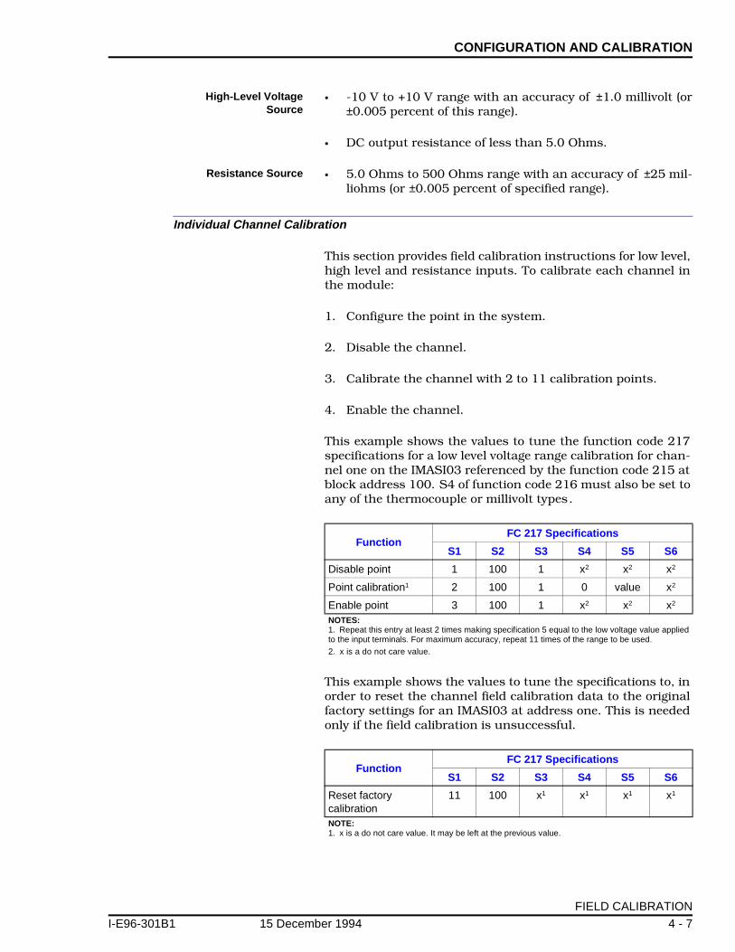
CONFIGURATION AND CALIBRATION
I-E96-301B
High-Level VoltageSource
• -10 V to +10 V range with an accuracy of ±1.0 millivolt (or±0.005 percent of this range).
• DC output resistance of less than 5.0 Ohms.
Resistance Source • 5.0 Ohms to 500 Ohms range with an accuracy of ±25 mil-liohms (or ±0.005 percent of specified range).
Individual Channel Calibration
This section provides field calibration instructions for low level,high level and resistance inputs. To calibrate each channel inthe module:
1. Configure the point in the system.
2. Disable the channel.
3. Calibrate the channel with 2 to 11 calibration points.
4. Enable the channel.
This example shows the values to tune the function code 217specifications for a low level voltage range calibration for chan-nel one on the IMASI03 referenced by the function code 215 atblock address 100. S4 of function code 216 must also be set toany of the thermocouple or millivolt types.
This example shows the values to tune the specifications to, inorder to reset the channel field calibration data to the originalfactory settings for an IMASI03 at address one. This is neededonly if the field calibration is unsuccessful.
FunctionFC 217 Specifications
S1 S2 S3 S4 S5 S6
Disable point 1 100 1 x2 x2 x2
Point calibration1 2 100 1 0 value x2
Enable point 3 100 1 x2 x2 x2
NOTES:1. Repeat this entry at least 2 times making specification 5 equal to the low voltage value appliedto the input terminals. For maximum accuracy, repeat 11 times of the range to be used.
2. x is a do not care value.
FunctionFC 217 Specifications
S1 S2 S3 S4 S5 S6
Reset factory calibration
11 100 x1 x1 x1 x1
NOTE:1. x is a do not care value. It may be left at the previous value.
FIELD CALIBRATION
1 15 December 1994 4 - 7

CONFIGURATION AND CALIBRATION ®
The following steps field calibrate channel 1 for the low-levelvoltage range of -100 mV to +100 mV. Change specification 4and use these steps to configure high level or resistanceinputs. Also S4 of function code 216 must be consistent withthe type of calibration being performed.
1. Locate the block address in the MFP of the EnhancedFunction Code (FC 217).
2. Verify that the slave expander bus dipshunts are in place toallow slave bus communications.
3. On the IMASI03, for each input channel, place the jumperconnector pairs (J1-J32) in position 1-2 for low or high voltageinputs (position 2-3 is for RTD inputs).
4. Set S2 of FC 217 to the block address of the function code215 which references the IMASI03.
5. Insert the slave into a powered slot. The LED will change tosolid green because the slave is linked to a function code 215in the configuration.
6. Allow the slave to warm up for at least 15 minutes.
7. Put the MFP in execute mode.
8. Set the FC 217 block for the required specifications. Aftereach calibration command is issued by performing a tune oper-ation, monitor the calibration command status to determine ifany errors have occurred during the field calibration.
This example calibrates channel one on the slave which is ref-erenced by the function code 215 at block address 100. For lowlevel voltage, disable the desired channel by tuning these val-ues into the specifications.
a. disable point S1 = 1
b. the slave referenced by FC 215 S2 = 100at block address 100
c. slave channel 1 S3 = 1
9. Verify that the low-level voltage source is connected tochannel 1 of the slave to be calibrated and the source voltage isset to the first desired value (this example calls for -100 mV).
NOTE: Each time the source voltage is changed, at least 15 sec-onds settling time is required before the point field calibration takesplace. If the source itself has a measurable settling time, add this tothe 15 second requirement.
FIELD CALIBRATION
4 - 8 15 December 1994 I-E96-301B1

CONFIGURATION AND CALIBRATION
I-E96-301B
10. Tune the FC 217 block specification 5 to the input voltageor resistance value. For this example, tune thesespecifications:
a. perform point calibration S1 = 2
b. the slave referenced by FC 215 S2 = 100at block address 100
c. slave channel 1 S3 = 1
d. calibration type 0 (low level) S4 = 0
e. calibration parameter 1 - 100 S5 = -100(millivolts)
Successful field calibration operations can be verified bychecking for a zero value in FC 217 blocks N+1 and N+4. If thepoint calibration was unsuccessful, an error code will appearin the FC 217 blocks N+1 and N+4 which can aid introubleshooting.
11. Change the calibration voltage (source output) to the nextdesired value (this example calls for -80 mV) and wait the 15second settling time.
12. Tune the FC 217 block to the next higher value in the cali-bration range. In this example, tune specification 5 to:
a. perform point calibration S1 = 2
b. the slave referenced by FC 215 S2 = 100at block address 100
c. slave channel 1 S3 = 1
d. calibration type 0 (low level) S4 = 0
e. calibration parameter 1 - 80 S5 = -80(millivolts)
13. Successful field calibration operations can be verified bychecking for a zero value in FC 217 blocks N+1 and N+4 for azero value. If the point calibration was unsuccessful, an errorcode will appear in the FC 217 blocks N+1 and N+4 which canaid in troubleshooting.
At this step two points have been field calibrated and theenable calibration command can be executed. For greaterchannel nonlinearity, calibrate additional points by repeatingSteps 7 through 12 for each additional point. A maximum of 11points can be specified for a given input range on each chan-nel. The three input ranges are low level, high level, or RTD.
FIELD CALIBRATION
1 15 December 1994 4 - 9

CONFIGURATION AND CALIBRATION ®
If desired, repeat Steps 7 through 12 for channels 2 through 16to calibrate all 16 channels on the slave.
14. Enable the point. Tune the FC 217 block specification 1 toenable the channel. For this example, tune thesespecifications:
a. enable the channel S1 = 3
b. the slave referenced by FC 215 S2 = 100at block address 100
c. slave channel 1 S3 = 1
d. calibration type x S4 = x1
e. calibration parameter x S5 = x
A successful enable operation can be verified by checking FC217 blocks N+1 and N+4 for a zero value. If the enable wasunsuccessful, an error code will appear in the FC 217 blocksN+1 and N+4 which can aid in troubleshooting.
A channel can be calibrated over the range used, even if it isonly part of the total range of the sensing device. For example,If the range of channel 1 was -100 mV to 0.0 mV enter -100mV, -90 mV, -80 mV (10 mV increments) up to 0.0 mV. Or ifthe range of channel 1 is -100 mV to -90 mV enter -100 mV,-99 mV, -98 mV, (1 mV increments) up to -90 mV.
This provides very accurate values from the slave to the MFPfor the range of the sensing device used (-100 mV to 0.0 mV,-100 mV to -90 mV).
1. x is a do not care value.
FIELD CALIBRATION
4 - 10 15 December 1994 I-E96-301B1
SECTION 5 - OPERATING PROCEDURES
I-E96-301B
INTRODUCTION
This section explains the start-up and operation for the Univer-sal Analog Input Slave Module (IMASI03).
START-UP
Communication between the IMASI03 slave and MFP masterstarts when the two modules are configured correctly (refer toSection 4). The slave address in Function Code 215 and 216must be the same as the address set on the address dipswitch.
Upon start-up, when power is applied to the IMASI03 and theMFP is put into execute mode, all channels are initially markedbad quality until the MFP downloads the configuration dataand the slave digitizes a valid input signal.
OPERATION
The MFP sends an interrupt command to the IMASI03 when-ever the MFP sends new configuration data. This interruptcauses the slave to read the configuration data and initialize itsinput handling, conversion, and compensation calculations.Once configured by the master, the IMASI03 slave scans itsinputs and makes corrected values available to the master overthe slave expander bus. The master reads the values from theslave during its normal segment cycle operations. Refer toSection 2 for more information about IMASI03 theory ofoperation.
ON-BOARD INDICATORS
The IMASI03 has one red/green LED indicator which showsthe operating status. The LED will:
• Flash red on power-up.
• Remain off after passing on board diagnostics until theIMASI03 is configured by the MFP.
• Show solid green after the master MFP downloads configu-ration data.
• Show solid green during normal running.
• Blink green when the MFP which configured the IMASI03enters configure mode from execute mode.
INTRODUCTION
5 - 1

OPERATING PROCEDURES ®
• Blink green if slave expander bus communication is lost (ifthe MFP is removed).
• Show solid red if a fatal failure of the IMASI03 moduleoccurs. For example, if power up diagnostics fail.
• Show solid red for a power fail interrupt (PFI).
• Show pass/fail of diagnostic routines when in diagnosticmode (refer to Section 6).
ON-BOARD INDICATORS
5 - 2 I-E96-301B

SECTION 6 - TROUBLESHOOTING
I-E96-301B
INTRODUCTION
This section explains the error signs and corrective actions forthe Universal Analog Input Slave Module (IMASI03).
ON-BOARD INDICATORS
The IMASI03 has one red/green LED indicator which showsthe operating status. The LED will:
• Flash red on power-up.
• Remain off after passing on board diagnostics until theIMASI03 is configured by the MFP.
• Show solid green after the master MFP downloads configu-ration data.
• Show solid green during normal running.
• Blink green when the MFP which configured the IMASI03enters configure mode from execute mode.
• Blink green if slave expander bus communication is lost (ifthe MFP is removed).
• Show solid red if a fatal failure of the IMASI03 moduleoccurs. For example, if power up diagnostics fail.
• Show solid red for a power fail interrupt (PFI).
• Show pass/fail of diagnostic routines when in diagnosticmode.
ALARM AND EXCEPTION REPORTING
No alarm or exception reports are generated directly by thefunction codes associated with the IMASI03. The values fromthe IMASI03 must be sent to a standard exception reportingblock if exception reporting is required. Refer to the instructionmanual for the operator interface being used for moreinformation.
PROBLEM REPORTS
Problem reports generated by the IMASI03 function codes (215and 216) are I/O slave error reports (Report Type 12).
INTRODUCTION
6 - 1
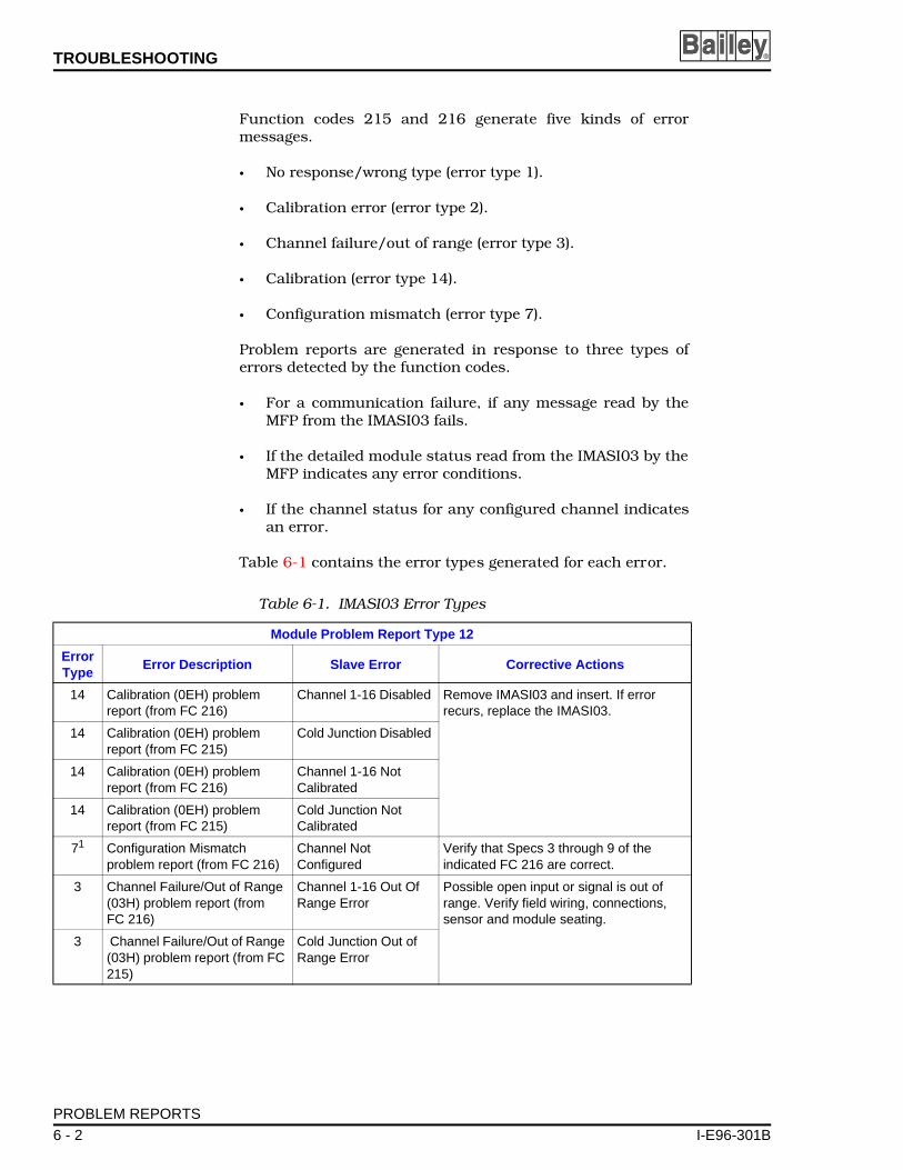
TROUBLESHOOTING ®
Function codes 215 and 216 generate five kinds of errormessages.
• No response/wrong type (error type 1).
• Calibration error (error type 2).
• Channel failure/out of range (error type 3).
• Calibration (error type 14).
• Configuration mismatch (error type 7).
Problem reports are generated in response to three types oferrors detected by the function codes.
• For a communication failure, if any message read by theMFP from the IMASI03 fails.
• If the detailed module status read from the IMASI03 by theMFP indicates any error conditions.
• If the channel status for any configured channel indicatesan error.
Table 6-1 contains the error types generated for each error.
Table 6-1. IMASI03 Error Types
Module Problem Report Type 12
Error Type
Error Description Slave Error Corrective Actions
14 Calibration (0EH) problem report (from FC 216)
Channel 1-16 Disabled Remove IMASI03 and insert. If error recurs, replace the IMASI03.
14 Calibration (0EH) problem report (from FC 215)
Cold Junction Disabled
14 Calibration (0EH) problem report (from FC 216)
Channel 1-16 Not Calibrated
14 Calibration (0EH) problem report (from FC 215)
Cold Junction Not Calibrated
71 Configuration Mismatch problem report (from FC 216)
Channel Not Configured
Verify that Specs 3 through 9 of the indicated FC 216 are correct.
3 Channel Failure/Out of Range (03H) problem report (from FC 216)
Channel 1-16 Out Of Range Error
Possible open input or signal is out of range. Verify field wiring, connections, sensor and module seating.
3 Channel Failure/Out of Range (03H) problem report (from FC 215)
Cold Junction Out of Range Error
PROBLEM REPORTS
6 - 2 I-E96-301B

TROUBLESHOOTING
I-E96-301B
3 Channel Failure/Out of Range (03H) problem report (from FC 216)
External Cold Junction Reference Error
Verify quality of block defined for Spec 3.
3 Channel Failure/Out of Range (03H) problem report (from FC 216)
Channel 1-16 A/D Conversion Error
Remove IMASI03 and insert. If error recurs, replace the IMASI03.
3 Channel Failure/Out of Range (03H) problem report (from FC 215)
Cold Junction A/D Conversion Error
2 Calibration (02H) problem report (from FC 215)
Unconfigured Reference Error
Cold junction reference is not zero and has bad quality. Unconfigured channel reference error (unused channel not functioning properly). The slave and all configured channels will continue to function properly.
2 Calibration Error (02H) problem report (from FC 215)
Cold Junction Reference Error
2 Calibration Error (02H) problem report (from FC 216)
Channel 1-16 Reference Error
Remove IMASI03 and insert. If error recurs, replace the IMASI03.
1 No Response/Wrong Type (01H) problem report (from FC 215)
Any Communication Failure. Any Command or Data Failure
1 No Response/Wrong Type (01H) problem report (from FC 215)
NVRAM Error
1 No Response/Wrong Type (01H) problem report (from FC 215)
Slave A/D Reference Error
1 Calibration Error (01H) problem report (from FC 215)
Slave Not Calibrated
1 No Response/Wrong Type (01H) problem report (from FC 216)
Channel 1-16 Slave Expander Bus Error
1 No Response/Wrong Type (01H) problem report (from FC 215)
Cold Junction Slave Expander Bus Error
Table 6-1. IMASI03 Error Types (continued)
Module Problem Report Type 12
Error Type
Error Description Slave Error Corrective Actions
PROBLEM REPORTS
6 - 3

TROUBLESHOOTING ®
ERROR MESSAGES AND CORRECTIVE ACTIONS
Input Channel Status
The slave maintains a fixed area in the dual port RAM to storethe current value and status of each channel. The master MFPreads the data and status for each channel individually.
To view the status of the IMASI03, read it's block output N+1 offunction code 215. Check the input status on each point indi-vidually by looking at the corresponding function code 216block output quality. Use any INFI 90 operator interface, suchas an Operator Interface Station (OIS) or Engineering WorkStation (EWS).
Slave Errors
Slave errors are reported to the MFP through function codes215 for the slave and 216 for the active input channels. TheMFP indicates slave errors through module status when in theexecute mode. Byte 1 of the module status will indicate anerror and byte 2 of the module status will indicate LIO (localI/O) when there is an IMASI03 error.
When specification 4 in function code 215 is set to 1, the MFPwill continue to execute if function code 215 detects an error. Amodule problem report can be requested in order to get specificinformation about any slave error indicated in module status.When specification 4 in function code 215 is set to 0, the MFPgoes into error mode if function code 215 detects an error. If anerror occurs, module status byte 1 will indicate an error, byte 2will indicate LIO and byte 3 will indicate the specific error.Refer to Table 6-2. For example, Analog Input Reference Erroris indicated by a 2 and Missing I/O is indicated by a 3 inbyte 3.
Table 6-2. Module Status (Byte 3) Error Codes
Error Code
Error Message
Description Corrective Actions
2 AIReference Error
The indicated FC 215 block failed due to an IMASI03 A/D system reference error.
Remove IMASI03 and insert. If error recurs, replace the IMASI03.
3 Missing I/O The indicated FC 215 block failed due to a communication error with the IMASI03.
Remove IMASI03, verify expander bus dip shunt, verify IMASI03 slave address is same as FC 215 Spec 1. Insert IMASI03 and verify proper seating. If error recurs, call Bailey field service.
The indicated FC 215 block detected an IMASI03 error. (IMASI03 slave firmware has reported an error.)
ERROR MESSAGES AND CORRECTIVE ACTIONS
6 - 4 I-E96-301B
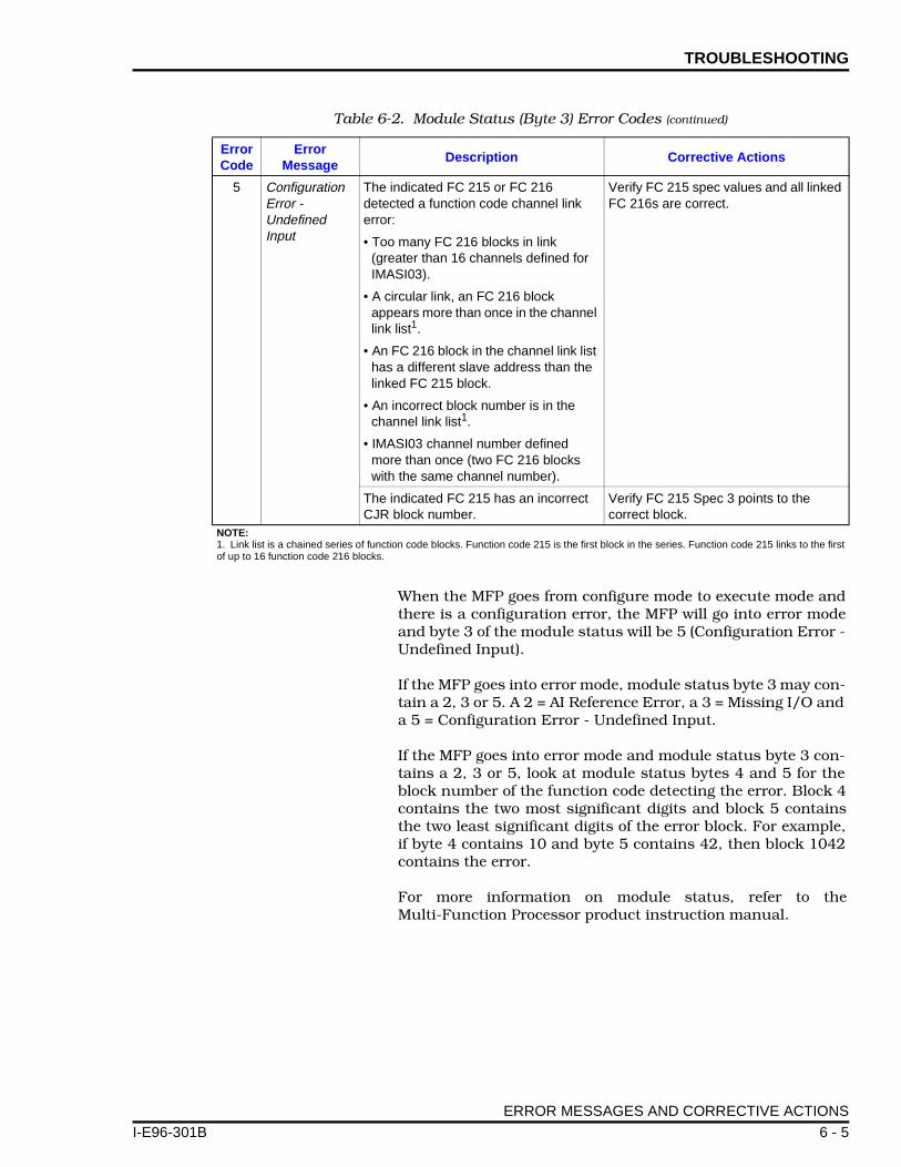
TROUBLESHOOTING
I-E96-301B
When the MFP goes from configure mode to execute mode andthere is a configuration error, the MFP will go into error modeand byte 3 of the module status will be 5 (Configuration Error -Undefined Input).
If the MFP goes into error mode, module status byte 3 may con-tain a 2, 3 or 5. A 2 = AI Reference Error, a 3 = Missing I/O anda 5 = Configuration Error - Undefined Input.
If the MFP goes into error mode and module status byte 3 con-tains a 2, 3 or 5, look at module status bytes 4 and 5 for theblock number of the function code detecting the error. Block 4contains the two most significant digits and block 5 containsthe two least significant digits of the error block. For example,if byte 4 contains 10 and byte 5 contains 42, then block 1042contains the error.
For more information on module status, refer to theMulti-Function Processor product instruction manual.
5 Configuration Error - Undefined Input
The indicated FC 215 or FC 216 detected a function code channel link error:
Verify FC 215 spec values and all linked FC 216s are correct.
• Too many FC 216 blocks in link (greater than 16 channels defined for IMASI03).
• A circular link, an FC 216 block appears more than once in the channel link list1.
• An FC 216 block in the channel link list has a different slave address than the linked FC 215 block.
• An incorrect block number is in the channel link list1.
• IMASI03 channel number defined more than once (two FC 216 blocks with the same channel number).
The indicated FC 215 has an incorrect CJR block number.
Verify FC 215 Spec 3 points to the correct block.
NOTE:1. Link list is a chained series of function code blocks. Function code 215 is the first block in the series. Function code 215 links to the firstof up to 16 function code 216 blocks.
Table 6-2. Module Status (Byte 3) Error Codes (continued)
Error Code
Error Message
Description Corrective Actions
ERROR MESSAGES AND CORRECTIVE ACTIONS
6 - 5
TROUBLESHOOTING ®
Error Example
Function code 215 for the slave and 216 for the active channelneed the same address. Check that the address on IMASI03switch SW1, the address in function code 215 specification 1and function code 216 specification 1 are the same.
If function code 216 slave address is not the same as functioncode 215 the MFP will go into error mode when put into exe-cute mode. The error will indicate 5, (byte 3 of module sta-tus/error message = 05) Configuration Error - UndefinedInput.
Modify the address in function code 215 and the associated216 blocks. The IMASI03 address value set in function code215 specification 1 and function code 216 specification 1should match the slave address set on SW1 on the IMASI03module.
Use an INFI 90 operator interface to change the configurationdata. For procedures on how to change a function code specifi-cation, refer to the product instruction manual for the operatorinterface being used.
The master module generates a local I/O error in the modulestatus if the slave expander bus is not connected between theslave module and the master module. Verify that the bus isconnected on the MMU backplane.
NOTE: Setting FC 215 specification 4 to 0 will cause the mastermodule to trip when the IMASI03 module fails. Changing specifica-tion 4 to a 1 causes the master module to continue to operate if theIMASI03 fails or is missing.
If both the 215 and 216 blocks have the wrong address, theMFP status will indicate a local I/O error. To correct this:
Remove the slave module and change the setting of SW1 onthe IMASI03 to match the module configuration settings.Refer to Section 3 for information on setting an addressand installing a slave module.
MODULE FUNCTIONAL TESTS
There are two sections in the slave functional test. Self-con-tained, dipswitch configurable diagnostics. Slave expander businterface testing (requires an MFP).
Test Equipment Requirements
To perform the functional testing, a single powered MMU slot(+5 V, ± 15 V, and power fail interrupt - PFI) is required. Slave
MODULE FUNCTIONAL TESTS
6 - 6 I-E96-301B

TROUBLESHOOTING
I-E96-301BI-E96-301B
expander bus testing requires a powered MMU slot, an MFP,an MFP interface device, and slave expander bus dipshunts.
Switch SW1 Settings
Table 6-3 lists the switch settings used in both parts of thefunctional test.
HALT - DISPLAY ERROR
SW1 pole position 2 is the error halt/continue bit. A one in thisposition when in diagnostics mode instructs the slave to stoptesting when an error is detected. The slave will loop on dis-playing the error code of the failed test.
If the test or group of tests passes, the LED will turn offmomentarily at the start of the test and display solid greenduring the test (or tests).
Table 6-3. Switch SW1 Settings, Operating Modesand Error Messages
SW1 Settings Operating Mode Error Code 1
0000000000000001
Initial switch settingModule address = 1
000000010000001000000100000010000001000000100000
1 Module addresses2 for the slave4 expander bus test81632
100000001x2000001
Dipswitch testWatchdog timer test
1x20001001x20001011x20001101x2000111
CPU testTimer testROM testAll tests (this group)
10111213
1x20010001x20010011x20010101x2001011
Dual-port RAM testNVRAM testSRAM testAll tests (this group)
20212223
1x20011001x20011011x20011101x2001111
16 channel low level reference testA/D reference test16 channel high level reference testAll tests (this group)
301
31401
33
1x2011111 All tests (10, 11, 12, 20, 21, 22, 30, 31)NOTES: 0 = ON = CLOSED; 1 = OFF = OPEN1. An error code of 30 or 40 will be followed by an error code indicating which input channel is notfunctional. For example, an error code of 30 followed by an error code of 7 indicates that channel7 is not functional. In this example, the LED will continue to display 30 and 7. The LED error se-quence repeats every 6 seconds.2. x = 0 Continue looping on tests. Do not display error.
x = 1 Halt on test failure. Display error code.
MODULE FUNCTIONAL TESTS
6 - 71 15 December 1994

TROUBLESHOOTING ®
If halt on error with display is selected a nd a specific test fails,an error code will be displayed by the status LED and repeatedevery six seconds. Refer to Table 6-3 for all of the error codes.
Example:
CONTINUE - DO NOT DISPLAY ERROR
When SW1 pole position 2 is set to a zero during diagnosticsmode, the slave will loop on running the selected tests. Loopingcontinues even if an error occurs. This mode is used to loop ona particular component in the event of a suspected failure.
If the continue - do not display error mode is selected, the LEDwill show solid green during the first iteration of the selectedtests. During the second test iteration, the LED will be off. TheLED will blink at a rate determined by the selected tests. Forexample, if all tests are selected, the LED will repeat asequence of being on for ten seconds and off for ten seconds.
Dipswitch Configurable Diagnostics
The diagnostic tests check these slave components:
• Slave Bus Address Switch• Watchdog Timer• Microprocessor • ROM• Static RAM• Dual-Port RAM (Slave read/write accesses)• Nonvolatile RAM• Individual Channel Voltage References• A/D Internal Voltage References
Test Procedure
DIPSWITCH TEST
1. Unplug the slave, set SW1 to the Dipswitch Test Mode asshown in Table 6-3, and insert the slave into the powered MMUslot. The status LED should immediately turn GREEN and stayGREEN.
Error Code 1 Green LED Blink Sequence
10 1 long blink (1 sec.) 0 short blinks (1/3 sec.)
11 1 long blink (1 sec.) 1 short blink (1/3 sec.)
12 1 long blink (1 sec.) 2 short blinks (1/3 sec.)NOTE:1. An error code of 30 will be followed by an error code indicating which input channel is not func-tional. For example, an error code of 30 followed by an error code of 7 indicates that channel 7 isnot functional.
MODULE FUNCTIONAL TESTS
6 - 8 I-E96-301B
TROUBLESHOOTING
I-E96-301B
2. With the slave still plugged into the powered MMU slot, tog-gle each dipswitch position of SW1 individually. As eachdipswitch position is toggled (from 0 to 1, and back to 0) indi-vidually, the status LED should change from GREEN to OFF,and back to GREEN again. Test all 8 dipswitch positions ofSW1.
ALL TESTS MODE
1. Unplug the slave and set SW1 to the All Tests Mode,Halt-Display Error, as shown in Table 6-3 (SW1 = 11011111).
2. Insert the slave into the powered MMU slot.
If the slave is passing the All Tests Mode diagnostics, the sta-tus LED will turn GREEN after 1 second and stay GREEN forabout 12 seconds. The status LED will then blink OFF andback to solid GREEN again within 1 second. The status LEDwill again stay green for about 12 seconds. Allow this cycle torepeat at least one additional time. If the All Tests Mode is suc-cessful, go to the Universal Slave Bus Test.
If the slave is failing the All Tests Mode and the halt/display onerror bit is set, the status LED will begin blinking an errorcode. The blinking LED represents a 2 digit error code. Findthe number by counting the number of times the status LEDblinks GREEN for long and short time periods. The two digitnumber can then be found in Table 6-3 (under Error Codes),and the problem can be identified.
Slave Expander Bus Interface Test
The following tests check for proper operation of these slaveexpander bus interface components.
• Slave Expander Bus interface chip.
• Dual-Port Static RAM (slave read/writes and MFPread/writes).
• MFP/IMASI03 slave handshaking.
Test Procedure
These two steps check for proper operation of the slave businterface:
1. Tune specification one of function code 217 to ten indicat-ing slave expander bus test. Also, tune specification two to theblock address of the slave's function code 215 block. Set allother specifications to the default value and send this block.
MODULE FUNCTIONAL TESTS
6 - 9
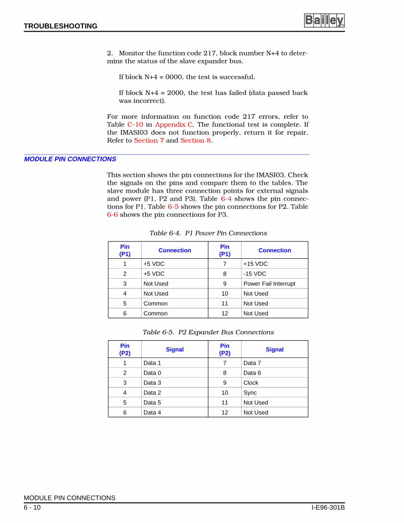
TROUBLESHOOTING ®
2. Monitor the function code 217, block number N+4 to deter-mine the status of the slave expander bus.
If block N+4 = 0000, the test is successful.
If block N+4 = 2000, the test has failed (data passed backwas incorrect).
For more information on function code 217 errors, refer toTable C-10 in Appendix C. The functional test is complete. Ifthe IMASI03 does not function properly, return it for repair.Refer to Section 7 and Section 8.
MODULE PIN CONNECTIONS
This section shows the pin connections for the IMASI03. Checkthe signals on the pins and compare them to the tables. Theslave module has three connection points for external signalsand power (P1, P2 and P3). Table 6-4 shows the pin connec-tions for P1. Table 6-5 shows the pin connections for P2. Table6-6 shows the pin connections for P3.
Table 6-4. P1 Power Pin Connections
Pin(P1)
ConnectionPin(P1)
Connection
1 +5 VDC 7 +15 VDC
2 +5 VDC 8 -15 VDC
3 Not Used 9 Power Fail Interrupt
4 Not Used 10 Not Used
5 Common 11 Not Used
6 Common 12 Not Used
Table 6-5. P2 Expander Bus Connections
Pin(P2)
SignalPin(P2)
Signal
1 Data 1 7 Data 7
2 Data 0 8 Data 6
3 Data 3 9 Clock
4 Data 2 10 Sync
5 Data 5 11 Not Used
6 Data 4 12 Not Used
MODULE PIN CONNECTIONS
6 - 10 I-E96-301B

TROUBLESHOOTING
I-E96-301B
Table 6-6. P3 Input Signal Pin Connections
Pin Signal Pin Signal
1 RTD- 26 RTD+
2 IN1+ 27 IN1-
3 COM1 28 COM2
4 IN2- 29 IN2+
5 IN3+ 30 IN3-
6 COM3 31 COM4
7 IN4- 32 IN4+
8 IN5+ 33 IN5-
9 COM5 34 COM6
10 IN6- 35 IN6+
11 IN7+ 36 IN7-
12 COM7 37 COM8
13 IN8- 38 IN8+
14 IN9+ 39 IN9-
15 COM9 40 COM10
16 IN10- 41 IN10+
17 IN11+ 42 IN11-
18 COM11 43 COM12
19 IN12- 44 IN12+
20 IN13+ 45 IN13-
21 COM13 46 COM14
22 IN14- 47 IN14+
23 IN15+ 48 IN15-
24 COM15 49 COM16
25 IN16- 50 IN16+
MODULE PIN CONNECTIONS
6 - 11

SECTION 7 - MAINTENANCE
I-E96-301B
INTRODUCTION
The Universal Analog Input Slave Module (IMASI03) needs littlemaintenance. Repair procedures are limited to module replace-ment. If the IMASI03 fails, remove and replace it with another.Verify that the switch settings on the replacement module arethe same as the failed module. This section contains a sched-ule to help take care of the system hardware. Refer questionsto your local Bailey Controls service office.
MAINTENANCE SCHEDULE
Do the tasks in Table 7-1 at the times shown.
Table 7-1. Maintenance Schedule
Task Interval
Clean and tighten each power and ground connection.
Every 6 months or at plant shut-down, whichever occurs first.
Use static safe vacuum cleaner to remove dust from:
ModulesModule Mounting UnitFan AssemblyPower Entry Panel
INTRODUCTION
7 - 1
SECTION 8 - REPAIR/REPLACEMENT PROCEDURES
I-E96-301B
INTRODUCTION
This section explains the replacement steps for a UniversalAnalog Input Slave Module (IMASI03). There are no specialtools required to replace an IMASI03 module.
MODULE REPAIR/REPLACEMENT
If the IMASI03 is faulty, replace it with a new one. DO NOT tryto repair the module; replacing components may affect themodule performance. Modules can be removed while systempower is supplied. To replace a module:
1. Push and turn the two front panel captive latches one halfturn to unlatch the module. It is unlatched when the slots onthe latches are vertical and the open end of the slots face awayfrom the center of the module.
2. Gently slide the module out of the MMU.
3. Configure the replacement module switch and jumper set-tings. Ensure they are set the same as the original module.
4. In the same slot assignment as the original module, alignthe replacement module with the guide rails in the MMU. Gen-tly slide it in until the front panel is flush with the top and bot-tom of the MMU frame.
5. Push and turn the two captive latches on the module face-plate one half turn to the latched position. It is latched whenthe slots on the latches are vertical and the open ends face thecenter of the module.
6. Return to normal operation.
INTRODUCTION
8 - 1

SECTION 9 - SUPPORT SERVICES
I-E96-301B
INTRODUCTION
Bailey Controls is ready to help you use, apply and repair itsproducts. Contact the nearest sales office to request servicesfor sales, repair and maintenance contracts. The sales officecan answer your questions on how to apply and install theBailey Controls INFI 90 system. They can help apply andinstall devices onto your system if it needs to be updated orexpanded.
REPLACEMENT PARTS AND ORDERING INFORMATION
When making repairs, be sure to order parts from a BaileyControls sales office. If you provide this information whenordering, it helps us to deliver the correct parts. Have this listready when calling in to order parts:
1. Part description, part number and quantity.
2. Model and serial numbers.
3. Bailey instruction manual number, page number and fig-ure that describe the part.
When ordering standard parts from Bailey Controls, use partnumbers and descriptions from the Recommended Spare PartsLists. Order parts without commercial descriptions from thenearest Bailey Controls sales office.
TRAINING
Bailey Controls has a modern training complex that providesservice and repair instruction. Service and repair trainingcourses can be held in your plant to train service personnel.Contact a Bailey Controls sales office for more information andto schedule training.
TECHNICAL DOCUMENTATION
Additional copies of this manual are available from the nearestBailey Controls sales office at a moderate charge. The currentmanuals for all products being offered can be ordered.
INTRODUCTION
9 - 1

APPENDIX A - NIAI05TERMINATION MODULE CONFIGURATION
I-E96-301B
INTRODUCTION
The Universal Analog Input Slave Module (IMASI03) uses twoNIAI05 termination modules to connect field wiring (eightinputs each). Jumpers on each NIAI05 configure each of theeight analog inputs for either system powered 4-20 mA, exter-nal powered 4-20 mA, 3-wire RTD, differential or single endedvoltage.
IMASI03 termination modules with both revision A and revi-sion B hardware are in service. This section contains informa-tion on revision A and B termination modules. See Figure A-1for the revision A module and Figure A-2 for the revision Bmodule.
Setup
The two NIAI05 termination modules should be installed nextto each other in the same termination module unit (TMU) ordirectly above and below each other in two separate TMUs. Thedistance between termination modules is limited by the dis-tance between J2 and J3 on the NKAS02 (or NKAS12) connec-tor cable.
Channel designation labels are provided with each NIAI05.This allows the user to configure one NIAI05 as the J2 termina-tion module for channels 1 through 8 and configure a secondNIAI05 as the J3 termination module for channels 9 through16. The J2 termination module connects to the NKAS02 (orNKAS12) connector labeled J2. The J3 termination moduleconnects to the NKAS02 (or NKAS12) J3 connector.
The NKAS02 connector cable has PVC insulation and is ratedfor 80o C (0 to 176o F) at 300 V (UL rated type CL2). TheNKAS12 connector cable has non-PVC insulation and is ratedfor 90o C (0 to 194o F) at 300 V (UL rated type PLTC).
Cold Junction Reference Input
Each NIAI05 termination module (two are required, even if only8 inputs or less are used) has an RTD which measures thetemperature of the termination module. This temperature isused to compensate for the cold junction effect on thermocou-ple inputs.
When using the built-in cold junction reference, the termina-tion module front cover should be in place. The cover enclosesboth the terminal blocks and the RTD. It helps maintain the
INTRODUCTION
A - 1
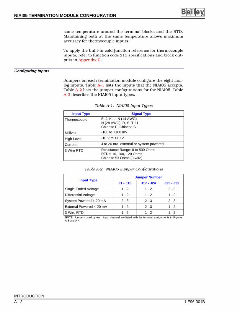
NIAI05 TERMINATION MODULE CONFIGURATION ®
same temperature around the terminal blocks and the RTD.Maintaining both at the same temperature allows maximumaccuracy for thermocouple inputs.
To apply the built-in cold junction reference for thermocoupleinputs, refer to function code 215 specifications and block out-puts in Appendix C.
Configuring Inputs
Jumpers on each termination module configure the eight ana-log inputs. Table A-1 lists the inputs that the NIAI05 accepts.Table A-2 lists the jumper configurations for the NIAI05. TableA-3 describes the NIAI05 input types.
Table A-1. NIAI05 Input Types
Input Type Signal Type
Thermocouple E, J, K, L, N (14 AWG) N (28 AWG), R, S, T, UChinese E, Chinese S.
Millivolt -100 to +100 mV
High Level -10 V to +10 V
Current 4 to 20 mA, external or system powered.
3 Wire RTD Resistance Range: 0 to 500 OhmsRTDs: 10, 100, 120 OhmsChinese 53 Ohms (3-wire)
Table A-2. NIAI05 Jumper Configurations
Input TypeJumper Number
J1 - J16 J17 - J24 J25 - J32
Single Ended Voltage 1 - 2 1 - 2 2 - 3
Differential Voltage 1 - 2 1 - 2 1 - 2
System Powered 4-20 mA 2 - 3 2 - 3 2 - 3
External Powered 4-20 mA 1 - 2 2 - 3 1 - 2
3-Wire RTD 1 - 2 1 - 2 1 - 2NOTE: Jumpers used by each input channel are listed with the terminal assignments in FiguresA-3 and A-4.
INTRODUCTION
A - 2 I-E96-301B

NIAI05 TERMINATION MODULE CONFIGURATION
I-E96-301B
Table A-3. NIAI05 Input Type Descriptions
Input Type Input Description
Single Ended Volt-age
This jumper configuration connects the minus (-) input terminal to I/O COM on the NIAI05. The IMASI03 measures the voltage at the plus (+) input terminal with respect to the I/O COM terminal. No connection to the C terminal is necessary.
Differential Voltage This jumper configuration connects the plus (+) and minus (-) inputs directly to IMASI03 differential input. Channel to channel and channel to system signal isolation is achieved for all voltage input types, including high level voltage, millivolts and thermocouples. No connection to the C terminal is necessary.
System Powered 4-20 mA
This jumper configuration connects the plus (+) input terminal to system +24 VDC through a current limiting resistor on NIAI05 modules with revision A hardware (revision B hardware replaces the resistor with a fuse). The minus (-) input terminal connects to a precision resistor that generates a single ended voltage (1 to 5 V) for the IMASI03 to measure. No connection to the C terminal is necessary. The INFI 90 system must have +24 volts (system power) installed.
External Powered 4-20 mA
This jumper configuration connects the plus (+) input terminal to one end of a precision resistor and the minus (-) input to the other end of the same precision resistor in the NIAI05. An isolated 1 to 5 Volts is generated for the IMASI03 to measure. No connection to the C terminal is necessary.
3-Wire Resistance This jumper configuration connects the plus (+) and minus (-) inputs and the C input directly to IMASI03 three-wire input. Channel to channel and channel to system signal isolation is maintained. The two common leads of the RTD element should be connected across the plus (+) and common (C) terminals, and the third lead should be connected to the minus (-) terminal.
INTRODUCTION
A - 3

NIAI05 TERMINATION MODULE CONFIGURATION ®
CONFIGURING INPUTS
This section contains figures of revision A and revision BIMASI03 termination modules.
• Figure A-1 shows the jumper locations on a module withrevision A hardware. Check jumpers before installing theNIAI05. Figure A-2 shows the jumper locations on a modulewith revision B hardware. Check jumpers before installingthe NIAI05.
• Figure A-3 shows the revision A hardware terminal assign-ments and the jumpers used for each input. Figure A-4shows the revision B hardware terminal assignments andthe jumpers used for each input.
• Figure A-5 shows a typical input circuit for the revision Ahardware NIAI05. Figure A-6 shows a typical input circuitfor the revision B hardware NIAI05.
• Figure A-7 shows revision A hardware field input termina-tion examples. Figure A-8 shows revision B hardware fieldinput termination examples.
• Figure A-9 shows revision A hardware IMASI03 inputexamples. Figure A-10 shows revision B hardware IMASI03input examples.
• Figure A-11 shows the cabling for the NIAI05 with revisionA or B hardware to the IMASI03. The NKAS02 (or NKAS12)cable connects the termination module to the IMASI03. TheNKAS02 cable has PVC insulation and is rated for 80 o C (0to 176o F) at 300 volts (UL rated type CL2). The NKAS12cable has non-PVC insulation and is rated for 90 o C (0 to194o F at 300 volts (UL rated type PLTC).
CONFIGURING INPUTS
A - 4 I-E96-301B

NIAI05 TERMINATION MODULE CONFIGURATION
I-E96-301B
Figure A-1. Jumper Locations for Revision A Hardware NIAI05
TP35258A
JUMPER CONFIGURATIONS
11 33 22
J1J17
J9J25
11 33 22
J2J18
J10J26
11 33 22
J7J23
J15J31
11 33 22
J6J22
J14J30
11 33 22
J5J21
J13J29
11 33 22
J4J20
J12J28
11 33 22
J3J19
J11J27
11 33 22
J8J24
J16J32
JUM
PE
RIN
ST
RU
CT
ION
S
SIN
GLE
-EN
DE
DV
OLT
AG
E
DIF
FE
RE
NTI
AL
VO
LTA
GE
SY
S-P
OW
ER
ED
4-20
mA
EX
T-P
OW
ER
ED
4-20
mA
3-W
IRE
RT
D
J1-J
16
1-2
1-2
2-3
1-2
1-2
J17
-J24
1-2
1-2
2-3
2-3
1-2
J25
-J32
2-3
1-2
2-3
1-2
1-2
CH
AN
NE
LS1-
8
J2C
CC
CC
CC
C
2623
2017
1411
85
329
AI1
AI2
AI3
AI4
AI5
AI6
AI7
AI8
––
––
––
––
2724
2118
1512
96
430
++
++
++
++
2825
2219
1613
107
3132
I/O COM
+24 VDC
CONFIGURING INPUTS
A - 5

NIAI05 TERMINATION MODULE CONFIGURATION ®
Figure A-2. Jumper Locations for Revision B Hardware NIAI05
TP35455A
JUMPER CONFIGURATIONS
NIAI0511 33 22
J1J17
J9J25
11 33 22
J2J18
J10J26
11 33 22
J7J23
J15J31
11 33 22
J6J22
J14J30
11 33 22
J5J21
J13J29
11 33 22
J4J20
J12J28
11 33 22
J3J19
J11J27
11 33 22
J8J24
J16J32
JUM
PE
RIN
ST
RU
CT
ION
S
SIN
GLE
-EN
DE
DV
OLT
AG
E
DIF
FE
RE
NT
IAL
VO
LTA
GE
SY
S-P
OW
ER
ED
4-20
mA
EX
T-P
OW
ER
ED
4-20
mA
3-W
IRE
RT
D
J1-J
16
1-2
1-2
2-3
1-2
1-2
J17
-J24
1-2
1-2
2-3
2-3
1-2
J25
-J32
2-3
1-2
2-3
1-2
1-2
CH
AN
NE
LS1-
8
J2C
CC
CC
CC
C
2623
2017
1411
85
29A
I1
TB
1T
B2
TB
3T
B4
AI2
AI3
AI4
AI5
AI6
AI7
AI8
––
––
––
––
2724
2118
1512
96
30
++
++
++
++
2825
2219
1613
107
3132
I/O COM
+24 VDC
GND
CONFIGURING INPUTS
A - 6 I-E96-301B
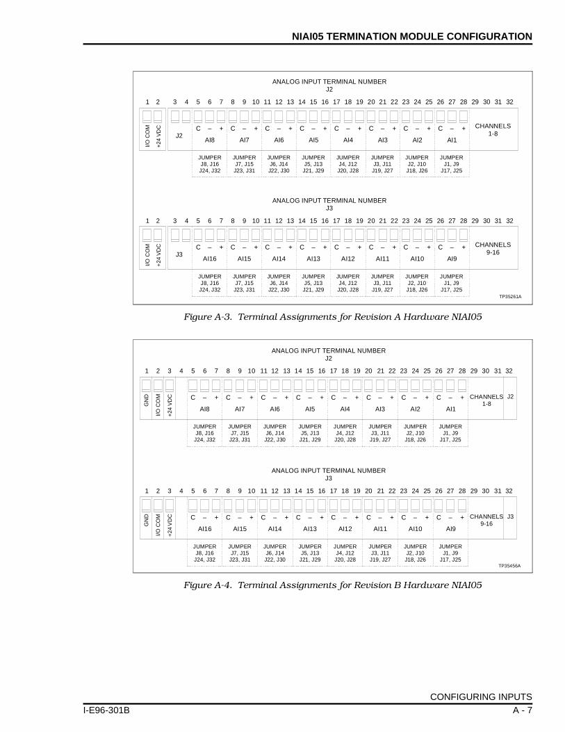
NIAI05 TERMINATION MODULE CONFIGURATION
I-E96-301B
Figure A-3. Terminal Assignments for Revision A Hardware NIAI05
Figure A-4. Terminal Assignments for Revision B Hardware NIAI05
C
C
C
C
C
C
C
C
C
C
C
C
C
C
C
C
–
–
AI8
AI16
J2
J3
CHANNELS1-8
CHANNELS9-16
JUMPERJ8, J16
J24, J32
JUMPERJ8, J16
J24, J32
JUMPERJ7, J15
J23, J31
JUMPERJ7, J15
J23, J31
JUMPERJ6, J14
J22, J30
JUMPERJ6, J14
J22, J30
JUMPERJ5, J13
J21, J29
JUMPERJ5, J13
J21, J29
JUMPERJ4, J12
J20, J28
JUMPERJ4, J12
J20, J28
JUMPERJ3, J11
J19, J27
JUMPERJ3, J11
J19, J27
JUMPERJ2, J10
J18, J26
JUMPERJ2, J10
J18, J26
JUMPERJ1, J9
J17, J25
JUMPERJ1, J9
J17, J25
–
–
AI7
AI15
–
–
AI6
AI14
–
–
AI5
AI13
–
–
AI4
AI12
–
–
AI3
AI11
–
–
AI2
AI10
–
–
AI1
AI9
+
+
+
+
+
+
+
+
+
+
+
+
+
+
+
+
3 324 5 6 7 8 9 10 11 12 13 14 15 16 17 18 19 20 21 22 23 24 25 26 27 28 29 30 311 2
3 324 5 6 7 8 9 10 11 12 13 14 15 16 17 18 19 20 21 22 23 24 25 26 27 28 29 30 311 2
I/OC
OM
I/OC
OM
+24
VD
C+
24V
DC
ANALOG INPUT TERMINAL NUMBERJ2
ANALOG INPUT TERMINAL NUMBERJ3
TP35261A
C
C
C
C
C
C
C
C
C
C
C
C
C
C
C
C
–
–
AI8
AI16
J2
J3
CHANNELS1-8
CHANNELS9-16
JUMPERJ8, J16
J24, J32
JUMPERJ8, J16
J24, J32
JUMPERJ7, J15
J23, J31
JUMPERJ7, J15
J23, J31
JUMPERJ6, J14
J22, J30
JUMPERJ6, J14
J22, J30
JUMPERJ5, J13
J21, J29
JUMPERJ5, J13
J21, J29
JUMPERJ4, J12
J20, J28
JUMPERJ4, J12
J20, J28
JUMPERJ3, J11J19, J27
JUMPERJ3, J11J19, J27
JUMPERJ2, J10
J18, J26
JUMPERJ2, J10
J18, J26
JUMPERJ1, J9
J17, J25
JUMPERJ1, J9
J17, J25
–
–
AI7
AI15
–
–
AI6
AI14
–
–
AI5
AI13
–
–
AI4
AI12
–
–
AI3
AI11
–
–
AI2
AI10
–
–
AI1
AI9
+
+
+
+
+
+
+
+
+
+
+
+
+
+
+
+
3
3
32
32
4
4
5
5
6
6
7
7
8
8
9
9
10
10
11
11
12
12
13
13
14
14
15
15
16
16
17
17
18
18
19
19
20
20
21
21
22
22
23
23
24
24
25
25
26
26
27
27
28
28
29
29
30
30
31
31
1
1
2
2
I/OC
OM
I/OC
OM
GN
DG
ND
+24
VD
C+
24V
DC
ANALOG INPUT TERMINAL NUMBERJ2
ANALOG INPUT TERMINAL NUMBERJ3
TP35456A
CONFIGURING INPUTS
A - 7
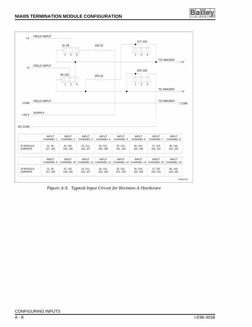
NIAI05 TERMINATION MODULE CONFIGURATION ®
Figure A-5. Typical Input Circuit for Revision A Hardware
+V
+V
–V
–V
COMCOM
+24 V
I/O COM
FIELD INPUT
FIELD INPUT
FIELD INPUT
SUPPLY
J1-J8
J9-J16J25-J32
J17-J24
TO IMASI03
TO IMASI03
TO IMASI03
150 Ω
250 Ω
1 1
1 1
2 2
2 2
3 3
3 3
INPUTCHANNEL 1
INPUTCHANNEL 9
INPUTCHANNEL 2
INPUTCHANNEL 10
INPUTCHANNEL 3
INPUTCHANNEL 11
INPUTCHANNEL 4
INPUTCHANNEL 12
INPUTCHANNEL 5
INPUTCHANNEL 13
INPUTCHANNEL 6
INPUTCHANNEL 14
INPUTCHANNEL 7
INPUTCHANNEL 15
INPUTCHANNEL 8
INPUTCHANNEL 16
J2 MODULEJUMPERS
J3 MODULEJUMPERS
J1, J9,J17, J25
J1, J9,J17, J25
J2, J10,J18, J26
J2, J10,J18, J26
J3, J11,J19, J27
J3, J11,J19, J27
J4, J12,J20, J28
J4, J12,J20, J28
J5, J13,J21, J29
J5, J13,J21, J29
J6, J14,J22, J30
J6, J14,J22, J30
J7, J15J23, J31
J7, J15J23, J31
J8, J16,J24, J32
J8, J16,J24, J32
TP35257A
CONFIGURING INPUTS
A - 8 I-E96-301B
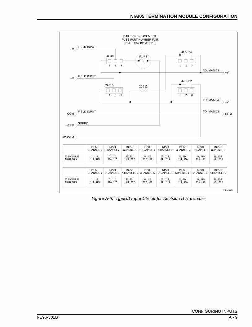
NIAI05 TERMINATION MODULE CONFIGURATION
I-E96-301B
Figure A-6. Typical Input Circuit for Revision B Hardware
+V
+V
–V
–V
COMCOM
+24 V
I/O COM
FIELD INPUT
FIELD INPUT
FIELD INPUT
SUPPLY
J1-J8
J9-J16J25-J32
J17-J24
TO IMASI03
TO IMASI03
TO IMASI03
F1-F8
BAILEY REPLACEMENTFUSE PART NUMBER FOR
F1-F8: 1945820A10310
250 Ω
1 1
1 1
2 2
2 2
3 3
3 3
INPUTCHANNEL 1
INPUTCHANNEL 9
INPUTCHANNEL 2
INPUTCHANNEL 10
INPUTCHANNEL 3
INPUTCHANNEL 11
INPUTCHANNEL 4
INPUTCHANNEL 12
INPUTCHANNEL 5
INPUTCHANNEL 13
INPUTCHANNEL 6
INPUTCHANNEL 14
INPUTCHANNEL 7
INPUTCHANNEL 15
INPUTCHANNEL 8
INPUTCHANNEL 16
J2 MODULEJUMPERS
J3 MODULEJUMPERS
J1, J9,J17, J25
J1, J9,J17, J25
J2, J10,J18, J26
J2, J10,J18, J26
J3, J11,J19, J27
J3, J11,J19, J27
J4, J12,J20, J28
J4, J12,J20, J28
J5, J13,J21, J29
J5, J13,J21, J29
J6, J14,J22, J30
J6, J14,J22, J30
J7, J15J23, J31
J7, J15J23, J31
J8, J16,J24, J32
J8, J16,J24, J32
TP35457A
CONFIGURING INPUTS
A - 9
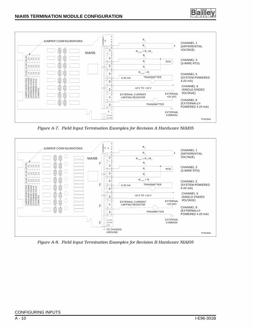
NIAI05 TERMINATION MODULE CONFIGURATION ®
IAL
WERED
Y--20 mA)
TP35266A
DED
)
IAL
WERED
Y--20 mA)
TP35458A
DED
)
Figure A-7. Field Input Termination Examples for Revision A Hardware NIAI05
4
Figure A-8. Field Input Termination Examples for Revision B Hardware NIAI05
JUMPER CONFIGURATIONS
NIAI0511 33 22
J1J17
J9J25
11 33 22
J2J18
J10J26
11 33 22
J7J23
J15J31
11 33 22
J6J22
J14J30
11 33 22
J5J21
J13J29
11 33 22
J4J20
J12J28
11 33 22
J3J19
J11J27
11 33 22
J8J24
J16J32
JUM
PE
RIN
ST
RU
CT
ION
SS
ING
LE-E
ND
ED
VO
LTA
GE
DIF
FE
RE
NT
IAL
VO
LTA
GE
SY
S-P
OW
ER
ED
4-20
mA
EX
T-P
OW
ER
ED
4-20
mA
3-W
IRE
RT
D
J1-J
16
1-2
1-2
2-3
1-2
1-2
J17-
J24
1-2
1-2
2-3
2-3
1-2
J25-
J32
2-3
1-2
2-3
1-2
1-2
CH
AN
NE
LS1-
8
CC
CC
CC
CC
2623
2017
1411
85
329
AI1
AI2
AI3
AI4
AI5
AI6
AI7
AI8
––
––
––
––
2724
21
1815
12
96
430
++
++
++
++
2825
2219
1613
107
3132
I/O COM
+24 VDC
J2
CHANNEL 1(DIFFERENTVOLTAGE)
RL1
RL
RTD
R = R +RLTOTA L L1 L2
R = RLTOTAL L
TRANSMITTER
TRANSMITTER
EXTERNAL CURRENTLIMITING RESISTOR
-10 V TO +10 V
EXTERNALCOMMON
EXTERNAL+24 VDC
+
–
4-20 mA
RL2
RL
RL
CHANNEL 5(SYSTEM-PO4-20 mA)
CHANNEL 8(EXTERNALLPOWERED 4
CHANNEL 6(SINGLE-ENVOLTAGE)
CHANNEL 3(3-WIRE RTD
JUMPER CONFIGURATIONS
NIAI0511 33 22
J1J17
J9J25
11 33 22
J2J18
J10J26
11 33 22
J7J23
J15J31
11 33 22
J6J22
J14J30
11 33 22
J5J21
J13J29
11 33 22
J4J20
J12J28
11 33 22
J3J19
J11J27
11 33 22
J8J24
J16J32
JUM
PE
RIN
ST
RU
CT
ION
SS
ING
LE-E
ND
ED
VO
LTA
GE
DIF
FE
RE
NT
IAL
VO
LTA
GE
SY
S-P
OW
ER
ED
4-20
mA
EX
T-P
OW
ER
ED
4-20
mA
3-W
IRE
RT
D
J1-J
16
1-2
1-2
2-3
1-2
1-2
J17-
J24
1-2
1-2
2-3
2-3
1-2
J25-
J32
2-3
1-2
2-3
1-2
1-2
CH
AN
NE
LS1-
8
J2C
CC
CC
CC
C
2623
2017
1411
85
29A
I1
TB
1T
B2
TB
3T
B4
AI2
AI3
AI4
AI5
AI6
AI7
AI8
––
––
––
––
2724
2118
1512
96
30
++
++
++
++
28
2522
1916
1310
731
32
I/O COM
+24 VDC
GND
CHANNEL 1(DIFFERENTVOLTAGE)
RL1
RL
RTD
R = R +RLTOTA L L1 L2
R = RLTOTAL L
TRANSMITTER
TRANSMITTER
EXTERNAL CURRENTLIMITING RESISTOR
-10 V TO +10 V
EXTERNALCOMMON
TO CHASSISGROUND
EXTERNAL+24 VDC
+
–
4-20 mA
RL2
RL
RL
CHANNEL 5(SYSTEM-PO4-20 mA)
CHANNEL 8(EXTERNALLPOWERED 4
CHANNEL 6(SINGLE-ENVOLTAGE)
CHANNEL 3(3-WIRE RTD
CONFIGURING INPUTS
A - 10 I-E96-301B

NIAI05 TERMINATION MODULE CONFIGURATION
I-E96-301B
Figure A-9. Revision A Hardware IMASI03 Input Examples
IMASI03
NKAS02/12CABLE
3-WIRE RTD
RLRL
RL
RL
RTD
+
–
C
ISOLATED FROM I/O COMMON
ISOLATEDCOMMON
TP35269A
IMASI03
NKAS02/12CABLE
I/O COM
-10 V TO +10 V
SINGLE-ENDEDVOLTAGE
VSO URCE
++
–
–
C
NON-ISOLATED
IMASI03
NKAS02/12CABLE
DIFFERENTIALVOLTAGE
RL1
RL2
+
–
C
IMASI03
NKAS02/12CABLE
+24 V
EXTERNAL+24 V
I/O COM
NON-ISOLATED
EXTERNAL COMMON
NIAI05 TERMINATION MODULE
SYSTEM-POWERED4-20 mA
1-5 V250
150TRANSMITTER
+
+
–
–C
IMASI03
NKAS02/12CABLE
EXTERNALLY-POWERED4-20 mA
1-5 V250
TRANSMITTER
EXTERNALCURRENTLIMITING
RESISTOR ++
– –
C
ISOLATED FROM I/O COMMON
ISOLATEDCOMMON
EXTERNALCOMMON
CONFIGURING INPUTS
A - 11

NIAI05 TERMINATION MODULE CONFIGURATION ®
Figure A-10. Revision B Hardware IMASI03 Input Examples
IMASI03
NKAS02/12CABLE
3-WIRE RTD
RLRL
RL
RL
RTD
+
–
C
ISOLATED FROM I/O COMMON
ISOLATEDCOMMON
TP35459A
IMASI03
NKAS02/12CABLE
I/O COM
-10 V TO +10 V
SINGLE-ENDEDVOLTAGE
VSO URCE
++
–
–
C
NON-ISOLATED
IMASI03
NKAS02/12CABLE
DIFFERENTIALVOLTAGE
RL1
RL2
+
–
C
IMASI03
NKAS02/12CABLE
+24 V
EXTERNAL+24 V
I/O COM
NON-ISOLATED
NIAI05 TERMINATION MODULE
SYSTEM-POWERED4-20 mA
1-5 V250
FUSETRANSMITTER
+
+
–
–C
IMASI03
NKAS02/12CABLE
EXTERNALLY-POWERED4-20 mA
1-5 V250
TRANSMITTER
EXTERNALCURRENTLIMITING
RESISTOR ++
– –
C
ISOLATED FROM I/O COMMON
ISOLATEDCOMMON
EXTERNALCOMMON
EXTERNAL COMMON
CONFIGURING INPUTS
A - 12 I-E96-301B
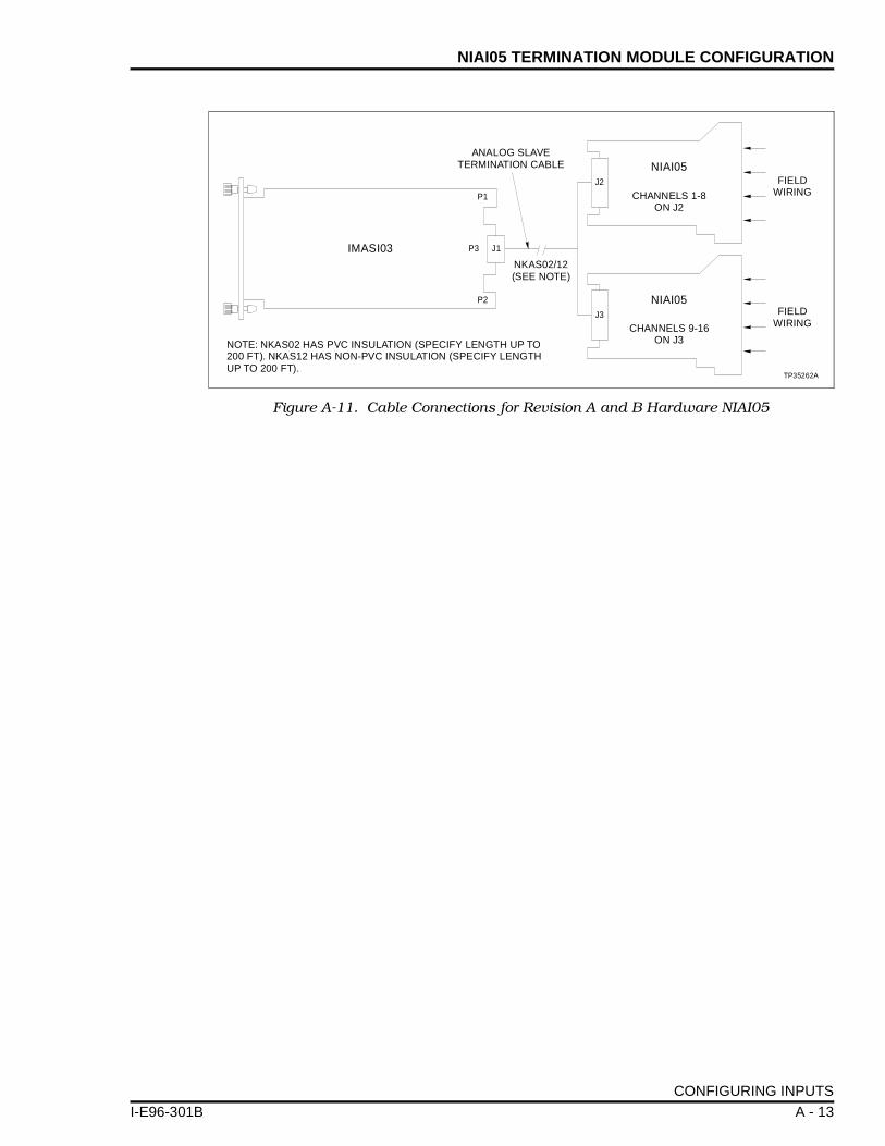
NIAI05 TERMINATION MODULE CONFIGURATION
I-E96-301B
Figure A-11. Cable Connections for Revision A and B Hardware NIAI05
TP35262A
P1
P3
J2
J3
J1
P2
NKAS02/12(SEE NOTE)
ANALOG SLAVETERMINATION CABLE NIAI05
NIAI05
CHANNELS 1-8ON J2
CHANNELS 9-16ON J3
IMASI03
FIELDWIRING
FIELDWIRING
NOTE: NKAS02 HAS PVC INSULATION (SPECIFY LENGTH UP TO200 FT). NKAS12 HAS NON-PVC INSULATION (SPECIFY LENGTHUP TO 200 FT).
CONFIGURING INPUTS
A - 13

APPENDIX B - NTAI06TERMINATION UNIT CONFIGURATION
I-E96-301B
INTRODUCTION
The Universal Analog Slave Input Module (IMASI03) uses oneNTAI06 Termination Unit for termination. Jumpers on theNTAI06 configure each of the 16 analog inputs for either sys-tem powered 4-20 mA, external powered 4-20 mA, 3-wire RTD,differential or single ended voltage.
IMASI03 termination units with both revision A and revision Bhardware are in service. This section contains information onrevision A and B units (see Figure B-1).
Cold Junction Reference Input
Each NTAI06 termination unit has a pair of RTDs which mea-sure the temperature of the termination unit. This temperatureis used to compensate for the cold junction effect on thermo-couple inputs.
When using the built-in cold junction reference, the termina-tion unit covers should be in place. The cover encloses both theterminal blocks and the RTD. It helps maintain the same tem-perature around the terminal blocks and the RTD. Maintainingboth at the same temperature allows maximum accuracy forthermocouple inputs.
To apply the built-in cold junction reference for thermocoupleinputs, refer to function code 215 specifications and block out-puts in Appendix C.
Configuring Inputs
Jumpers on the termination unit configure the 16 analoginputs. Table B-1 lists the inputs that the NTAI06 accepts.Table B-2 lists the jumper configurations for the NTAI06. TableB-3 describes the NTAI06 input types.
INTRODUCTION
B - 1

NTAI06 TERMINATION UNIT CONFIGURATION ®
Table B-1. NTAI06 Input Types
Input Type Signal Type
Thermocouple E, J, K, L, N (14 AWG) N (28 AWG), R, S, T, UChinese E, Chinese S.
Millivolt -100 to +100 mV
High Level -10 V to +10 V
Current 4 to 20 mA, external or system powered.
3-Wire RTD Resistance Range: 0 to 500 OhmsRTDs: 10, 100, 120 OhmsChinese 53 Ohms (3-wire)
Table B-2. NTAI06 Jumper Configurations
Input TypeJumper Number
J1 - J32 J33 - J48 J49 - J64
Single Ended Voltage 1 - 2 1 - 2 2 - 3
Differential Voltage 1 - 2 1 - 2 1 - 2
System Powered 4-20 mA 2 - 3 2 - 3 2 - 3
External Powered 4-20 mA 1 - 2 2 - 3 1 - 2
3-Wire RTD 1 - 2 1 - 2 1 - 2NOTE: Jumpers used by each input channel are listed with the terminal assignments in Figure B-3.
Table B-3. NTAI06 Input Type Descriptions
Input Type Input Description
Single Ended Voltage
This jumper configuration connects the minus(-) input terminal to I/O COM on the NTAI06. The IMASI03 measures the voltage at the plus (+) input terminal with respect to the C terminal. No connection to the C terminal is necessary.
Differential Voltage
This jumper configuration connects the plus (+) and minus (-) inputs directly to IMASI03 differential input. Channel to channel and channel to system signal isolation is achieved for all voltage input types, including high level voltage, millivolts and thermocouples. No connection to the C terminal is necessary.
System Powered 4-20 mA
This jumper configuration connects the plus (+) input terminal to system +24 VDC through a fuse on the NTAI06. The minus (-) input terminal connects to a precision resistor that generates a single ended voltage (1 to 5 V) for the IMASI03 to measure. No connection to the C terminal is necessary. INFI 90 must have +24 Volts (system power) installed.
External Powered 4-20 mA
This jumper configuration connects the plus (+) input terminal to one end of a precision resistor and the minus (-) input to the other end of the same precision resistor in the NTAI06. An isolated 1 to 5 Volts is generated for the IMASI03 to measure. No connection to the C terminal is necessary.
3-Wire Resistance
This jumper configuration connects the plus (+) and minus (-) inputs and the COM input directly to IMASI03 three-wire input. Channel to channel and channel to system signal isolation is maintained. The two common leads of the RTD element should be connected across the plus (+) and common (C) terminals, and the third lead should be connected to the minus (-) terminal.
INTRODUCTION
B - 2 I-E96-301B

NTAI06 TERMINATION UNIT CONFIGURATION
I-E96-301B
CONFIGURING INPUTS
This section contains figures of revision A and revision BIMASI03 termination units.
• Figure B-1 shows the jumper locations and terminalassignments for revision A hardware. Check jumpersbefore installing the NTAI06. Figure B-2 shows the jumperlocations and terminal assignments for revision B hard-ware. Check jumpers before installing the NTAI06.
• Figure B-3 shows a typical input circuit and the jumpersused for each input.
• Figure B-4 shows field input termination examples for revi-sion A and B hardware.
• Figure B-5 shows IMASI03 input examples.
• Figure B-6 shows the cabling for the IMASI03. The NKAS01(or NKAS11) cable connects the termination unit to theIMASI03. The NKAS01 cable has PVC insulation and israted for 80o C (0 to 176o F) at 300 V (UL rated type CL2).The NKAS11 cable has non-PVC insulation and is rated for90o C (0 to 194o F) at 300 V (UL rated type PLTC).
CONFIGURING INPUTS
B - 3
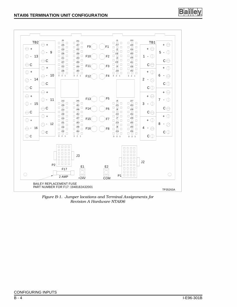
NTAI06 TERMINATION UNIT CONFIGURATION ®
Figure B-1. Jumper locations and Terminal Assignments for Revision A Hardware NTAI06
TB1TB2
E2E1
P1
TP35263A
COM+24V2 AMP
P2
+
-
C
13
+
-
C
+
-
C
+
-
C
16
15
14
+
-
C
+
-
C
+
-
C
+
-
C
9
10
11
12
+
-
C
+
-
C
+
-
C
+
-
C
+
-
C
+
-
C
+
-
C
+
-
C
1
2
5
6
37
48
J1
J17
J2
J18
J19
J4
J20
J3
J33
J49
J34
J50
J35
J51
J36
J52
J37
J53
J38
J54
J39
J55
J40
J56
J5
J21
J6
J22
J7
J23
J8
J24
J9
J25
J10
J26
J11
J27
J12
J28
J41
J57
J42
J58
J43
J59
J44
J60
J13
J29
J14
J30
J15
J31
J16
J32
J45
J61
J46
J62
J47
J63
J48
J64
3 2 13 2 1 3 2 1
3 2 1 3 2 1 3 2 1 3 2 1
3 2 1
F17
F1
F2
F3
F4
F5
F6
F7
F8
F9
F10
F11
F12
F13
F14
F15
F16
BAILEY REPLACEMENT FUSEPART NUMBER FOR F17: 1948182A32001
J3
J2
CONFIGURING INPUTS
B - 4 I-E96-301B

NTAI06 TERMINATION UNIT CONFIGURATION
I-E96-301B
Figure B-2. Jumper Locations and Terminal Assignments for Revision B Hardware NTAI06
TP35460A
NOTE: ATTACH MOUNTING SCREWTO CONNECT CHASSIS GROUND
TB1TB2
E2E1
P1COM+24V
P2
+
-
C
13
+
-
C
+
-
C
+
-
C
16
15
14
+
-
C
+
-
C
+
-
C
+
-
C
9
10
11
12
+
-
C
+
-
C
+
-
C
+
-
C
+
-
C
+
-
C
+
-
C
+
-
C
1
2
5
6
37
48
J1
J17
J2
J18
J19
J4
J20
J3
J33
J49
J34
J50
J35
J51
J36
J52
J37
J53
J38
J54
J39
J55
J40
J56
J5
J21
J6
J22
J7
J23
J8
J24
J9
J25
J10
J26
J11
J27
J12
J28
J41
J57
J42
J58
J43
J59
J44
J60
J13
J29
J14
J30
J15
J31
J16
J32
J45
J61
J46
J62
J47
J63
J48
J64
3 2 1 3 2 1
3 2 1 3 2 13 2 1 3 2 1
3 2 1 3 2 1
F1
F2
F3
F4
F5
F6
F7
F8
F9
F10
F11
F12
F13
F14
F15
F16
GND
J2
J3
CONFIGURING INPUTS
B - 5
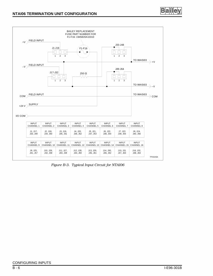
NTAI06 TERMINATION UNIT CONFIGURATION ®
Figure B-3. Typical Input Circuit for NTAI06
+V
+V
–V
–V
COMCOM
+24 V
I/O COM
FIELD INPUT
FIELD INPUT
FIELD INPUT
SUPPLY
J1-J16
J17-J32J49-J64
J33-J48
TO IMASI03
TO IMASI03
TO IMASI03
F1-F16
BAILEY REPLACEMENTFUSE PART NUMBER FOR
F1-F16: 1945820A10310
250 Ω
1 1
1 1
2 2
2 2
3 3
3 3
INPUTCHANNEL 1
INPUTCHANNEL 9
INPUTCHANNEL 2
INPUTCHANNEL 10
INPUTCHANNEL 3
INPUTCHANNEL 11
INPUTCHANNEL 4
INPUTCHANNEL 12
INPUTCHANNEL 5
INPUTCHANNEL 13
INPUTCHANNEL 6
INPUTCHANNEL 14
INPUTCHANNEL 7
INPUTCHANNEL 15
INPUTCHANNEL 8
INPUTCHANNEL 16
J1, J17,J33, J49
J9, J25,J41, J57
J2, J18,J34, J50
J10, J26,J42, J58
J3, J19,J35, J51
J11, J27,J43, J59
J4, J20,J36, J52
J12, J28,J44, J60
J5, J21,J37, J53
J13, J29,J45, J61
J6, J22,J38, J54
J14, J30,J46, J62
J7, J23J39, J55
J15, J31J47, J63
J8, J24,J40, J56
J16, J32,J48, J64
TP35259A
CONFIGURING INPUTS
B - 6 I-E96-301B
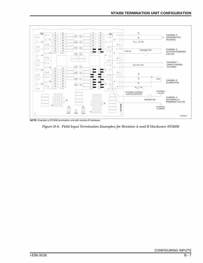
NTAI06 TERMINATION UNIT CONFIGURATION
I-E96-301B
Fi
TB2
+
-
C
13
+
-
C
+
-
C
+
-
C
16
15
14
NOTE: Examp
gure B-4. Field Input Termination Examples for Revision A and B Hardware NTAI06
TB1
E2E1
P1COM+24V
P2
+
-
C
+
-
C
+
-
C
+
-
C
9
10
11
12
+
-
C
+
-
C
+
-
C
+
-
C
+
-
C
+
-
C
+
-
C
+
-
C
1
2
5
6
3
7
4
8
J1
J17
J2
J18
J19
J4
J20
J3
J33
J49
J34
J50
J35
J51
J36
J52
J37
J53
J38
J54
J39
J55
J40
J56
J5
J21
J6
J22
J7
J23
J8
J24
J9
J25
J10
J26
J11
J27
J12
J28
J41
J57
J42
J58
J43
J59
J44
J60
J13
J29
J14
J30
J15
J31
J16
J32
J45
J61
J46
J62
J47
J63
J48
J64
3 2 1 3 2 1 3 2 1 3 2 1
3 2 13 2 13 2 13 2 1
F1
F2
F3
F4
F5
F6
F7
F8
F9
F10
F11
F12
F13
F14
F15
F16
GND
TP35461A
NTA
I06
J3
J2
CHANNEL 5(DIFFERENTIALVOLTAGE)
CHANNEL 6(SYSTEM-POWERED4-20 mA)
CHANNEL 4(EXTERNALLY-POWERED 4-20 mA)
CHANNEL 7(SINGLE-ENDEDVOLTAGE)
CHANNEL 8(3-WIRE RTD)
RL1
R = R +RLTOTAL L1 L2
-10 V TO +10 V
EXTERNALCOMMON
+
–
4-20 mA
RL2
RL
RTD
R = RLTOTAL L
RL
RL
TRANSMITTER
TRANSMITTER
EXTERNAL CURRENTLIMITING RESISTOR
EXTERNAL+24 VDC
le is NTAI06 termination unit with revision B hardware.
CONFIGURING INPUTS
B - 7
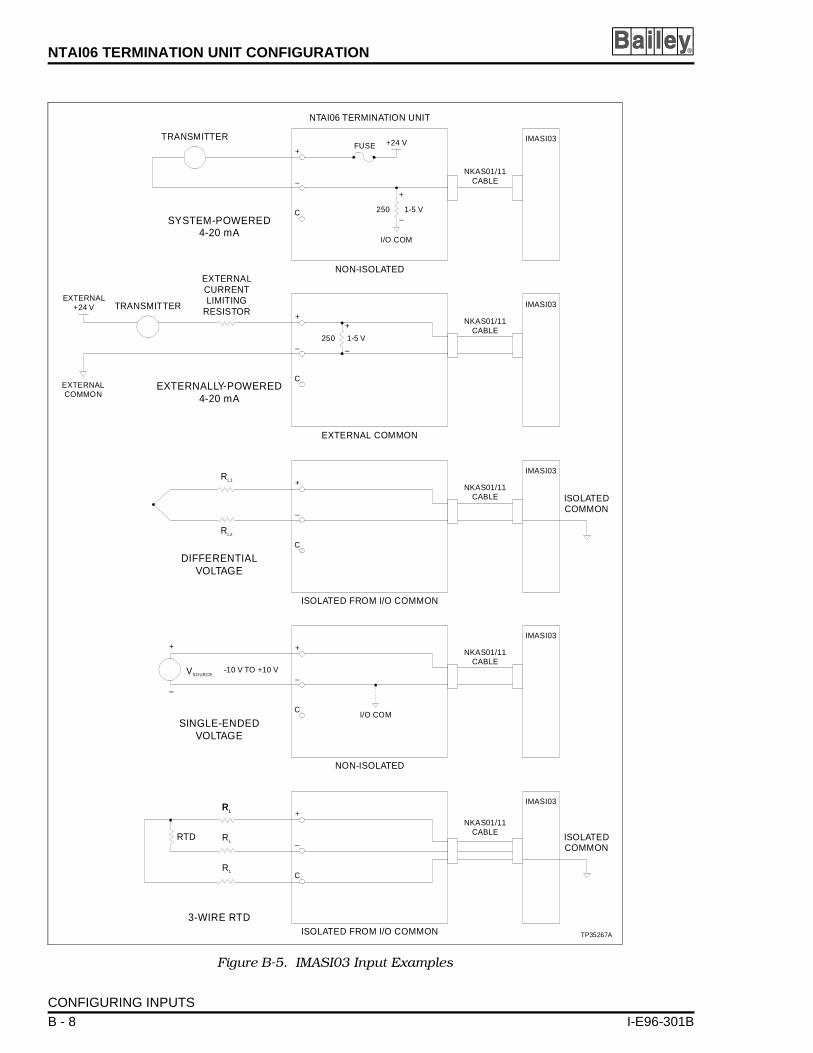
NTAI06 TERMINATION UNIT CONFIGURATION ®
Figure B-5. IMASI03 Input Examples
IMASI03
NKAS01/11CABLE
3-WIRE RTD
RL
RL
RL
RL
RTD
+
–
C
ISOLATED FROM I/O COMMON
ISOLATEDCOMMON
TP35267A
IMASI03
NKAS01/11CABLE
I/O COM
-10 V TO +10 V
SINGLE-ENDEDVOLTAGE
VSO URCE
++
–
–
C
NON-ISOLATED
IMASI03
NKAS01/11CABLE
DIFFERENTIALVOLTAGE
RL1
RL2
+
–
C
IMASI03
NKAS01/11CABLE
+24 V
EXTERNAL+24 V
I/O COM
NON-ISOLATED
NTAI06 TERMINATION UNIT
SYSTEM-POWERED4-20 mA
1-5 V250
FUSETRANSMITTER
+
+
–
–C
IMASI03
NKAS01/11CABLE
EXTERNALLY-POWERED4-20 mA
1-5 V250
TRANSMITTER
EXTERNALCURRENTLIMITING
RESISTOR+
+
– –
C
ISOLATED FROM I/O COMMON
EXTERNAL COMMON
ISOLATEDCOMMON
EXTERNALCOMMON
CONFIGURING INPUTS
B - 8 I-E96-301B

NTAI06 TERMINATION UNIT CONFIGURATION
I-E96-301B
Figure B-6. Cable Connections for NTAI06
TP35256A
P1
P3
J3
J2
J1
P2
NKAS01/11(SEE NOTE)
ANALOG SLAVETERMINATION UNIT CABLE
NTAI06
CHANNELS 11-16
CHANNELS 1-10
IMASI03FIELD
WIRING
NOTE: NKAS01 HAS PVC INSULATION (SPECIFY LENGTH UP TO200 FT). NKAS11 HAS NON-PVC INSULATION (SPECIFY LENGTHUP TO 200 FT).
CONFIGURING INPUTS
B - 9

APPENDIX C - FUNCTION CODE DEFINITIONS
I-E96-301B
INTRODUCTION
The IMASI03 Universal Analog Input Slave Module is config-ured and controlled through function blocks configured on themaster MFP. This section describes the three function codesthat support the IMASI03. They are FC 215, FC 216 and FC217.
All specifications in function codes 215, 216 and 217 associ-ated with the IMASI03 may be changed during on-line configu-ration. When changes are made to the input channelparameters (FC 216), the channel will hold the last value withstatus unchanged for a short period. This hold time is based onthe number of channels that were changed during on-line con-figuration, as well as the resolution specified in the functioncode 216 blocks for that channel. Plan on a hold time of fourseconds (worst case) for each function code 216 changed dur-ing on-line configuration.
The function code information in this appendix is for referenceonly. Refer to the Function Code Application Manual,I-E93-900-20 for current information on the function codes.
ENHANCED ANALOG SLAVE DEFINITION FUNCTION CODE (FC 215)
This function code is used to define an analog slave module tothe MFP.
The Enhanced Analog Slave Definition Function Code (FC215)defines the common specifications for the IMASI03 module.Individual input function code 216 blocks are linked to thisblock to define the channels available on an IMASI03. Functioncode 215 uses 30 bytes of NVRAM and 206 bytes of RAM mem-ory in the MFP module.
This function block has three outputs. The first represents thecold-junction reference input in degrees C from the analogslave input module termination device. The second output is aBoolean value representing the overall status of the slave mod-ule. The third output gives the actual scan cycle time in sec-onds for all of the active inputs on the slave.
Table C-1 lists the outputs of function code 215. Table C-2 liststhe output descriptions of function code 215. Table C-3 liststhe specifications of function code 215.
INTRODUCTION
C - 1
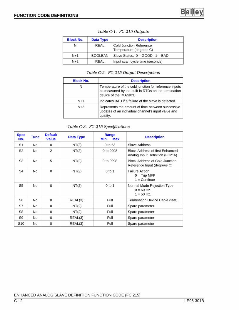
FUNCTION CODE DEFINITIONS ®
Table C-1. FC 215 Outputs
Block No. Data Type Description
N REAL Cold Junction ReferenceTemperature (degrees C)
N+1 BOOLEAN Slave Status: 0 = GOOD; 1 = BAD
N+2 REAL Input scan cycle time (seconds)
Table C-2. FC 215 Output Descriptions
Block No. Description
N Temperature of the cold junction for reference inputs as measured by the built-in RTDs on the termination device of the IMASI03.
N+1 Indicates BAD if a failure of the slave is detected.
N+2 Represents the amount of time between successive updates of an individual channel's input value and quality.
Table C-3. FC 215 Specifications
Spec No.
TuneDefault Value
Data TypeRange
Min. MaxDescription
S1 No 0 INT(2) 0 to 63 Slave Address
S2 No 2 INT(2) 0 to 9998 Block Address of first Enhanced Analog Input Definition (FC216)
S3 No 5 INT(2) 0 to 9998 Block Address of Cold JunctionReference Input (degrees C)
S4 No 0 INT(2) 0 to 1 Failure Action0 = Trip MFP1 = Continue
S5 No 0 INT(2) 0 to 1 Normal Mode Rejection Type0 = 60 Hz.1 = 50 Hz.
S6 No 0 REAL(3) Full Termination Device Cable (feet)
S7 No 0 INT(2) Full Spare parameter
S8 No 0 INT(2) Full Spare parameter
S9 No 0 REAL(3) Full Spare parameter
S10 No 0 REAL(3) Full Spare parameter
ENHANCED ANALOG SLAVE DEFINITION FUNCTION CODE (FC 215)
C - 2 I-E96-301B
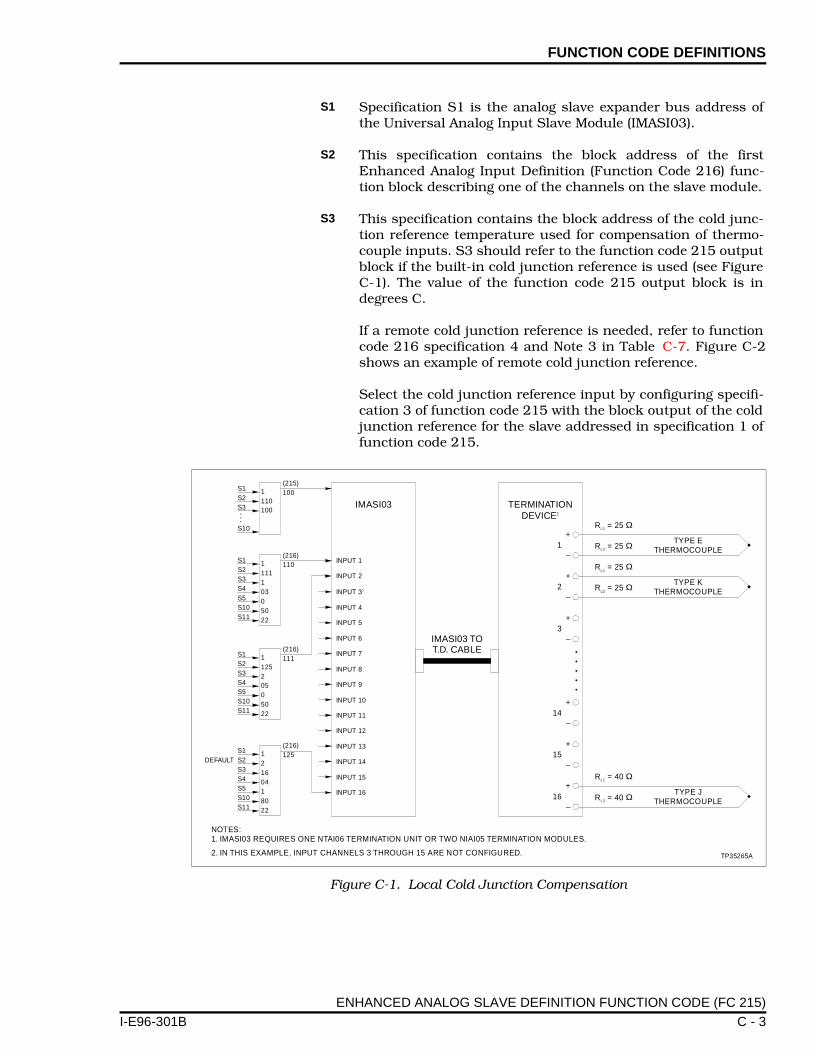
FUNCTION CODE DEFINITIONS
I-E96-301B
S1 Specification S1 is the analog slave expander bus address ofthe Universal Analog Input Slave Module (IMASI03).
S2 This specification contains the block address of the firstEnhanced Analog Input Definition (Function Code 216) func-tion block describing one of the channels on the slave module.
S3 This specification contains the block address of the cold junc-tion reference temperature used for compensation of thermo-couple inputs. S3 should refer to the function code 215 outputblock if the built-in cold junction reference is used (see FigureC-1). The value of the function code 215 output block is indegrees C.
If a remote cold junction reference is needed, refer to functioncode 216 specification 4 and Note 3 in Table C-7. Figure C-2shows an example of remote cold junction reference.
Select the cold junction reference input by configuring specifi-cation 3 of function code 215 with the block output of the coldjunction reference for the slave addressed in specification 1 offunction code 215.
Figure C-1. Local Cold Junction Compensation
R = 25L1 Ω
TYPE ETHERMOCOUPLER = 25L2 Ω
R = 25L1
Ω
TYPE KTHERMOCOUPLER = 25
L2Ω
IMASI03
IMASI03 TOT.D. CABLE
TERMINATIONDEVICE1
(215)100
(216)110
(216)111
(216)125
INPUT 1
INPUT 2
INPUT 3
INPUT 4
2
INPUT 5
INPUT 6
INPUT 7
INPUT 8
INPUT 9
INPUT 10
INPUT 11
INPUT 12
INPUT 13
INPUT 14
INPUT 15
INPUT 16
S1S2S3
S1S2S3S4S5S10S11
S1S2S3S4S5S10S11
S1S2S3S4S5S10S11
DEFAULT
1110100
111110305022
112520505022
12160418022
S10
•••
•••••
NOTES:1. IMASI03 REQUIRES ONE NTAI06 TERMINATION UNIT OR TWO NIAI05 TERMINATION MODULES.
2. IN THIS EXAMPLE, INPUT CHANNELS 3 THROUGH 15 ARE NOT CONFIGURED. TP35265A
+
+
+
+
+
+
–
–
–
–
–
–
1
14
2
15
3
16
R = 40L1 Ω
TYPE JTHERMOCOUPLER = 40L2 Ω
ENHANCED ANALOG SLAVE DEFINITION FUNCTION CODE (FC 215)
C - 3

FUNCTION CODE DEFINITIONS ®
SOUPLE
ROUPLE
TP35264A
TOUPLE
USEDION
S4 This specification identifies the action to be taken in the eventof a failure of the slave module (such as NVRAM, A/D refer-ence, or ROM checksum errors). A zero indicates that the MFPshould cease operation while a one indicates the MFP shouldcontinue operation.
S5 This specification identifies the dominant noise frequency to berejected during the analog-to-digital conversion operation (50or 60 Hertz).
S6 This specification gives the length of the cable between the ter-mination device and the slave module. This is used by the slaveto compensate the measured input value for effects of resis-tance in the cable. This adjustment is similar to that for leadwire resistance of the field input lead wires.
S7-S10 Spare parameters.
Figure C-2. Remote Cold Junction Compensation
R = 30L1 Ω2
TYPETHERMOCR = 30L2 Ω
R = 20L1 Ω
TYPETHERMOCR = 20
L2 Ω
IMASI03 REMOTETERMINAL
BLOCK
IMASI03 TOT.D. CABLE
TERMINATIONDEVICE1
(215)100
(216)110
(216)111
(216)124
(216)125
INPUT 1
INPUT 2
INPUT 3
INPUT 4
3
INPUT 5
INPUT 6
INPUT 7
INPUT 8
INPUT 9
INPUT 10
INPUT 11
INPUT 12
INPUT 13
INPUT 14
INPUT 15
INPUT 16
S1S2S3
S1S2S3S4S5S10S11
S1S2S3S4S5S10S11
S1S2S3S4S5S10S11
S1S2S3S4S5S10S11
DEFAULT
1110125
111110106022
112420204022
1125150605022
121610403022
S10
•••
•••••
NOTES:1. IMASI03 REQUIRES ONE NTAI06 TERMINATION UNIT OR TWO NIAI05 TERMINATION MODULES.
2. TOTAL CABLE RESISTANCE IS CALCULATED FROM THE TERMINATION DEVICE TO THETHERMOCOUPLE. PUT THIS VALUE INTO FC 216 SPECIFICATION 10.
3. IN THIS EXAMPLE, INPUT CHANNELS 3 THROUGH 14 ARE NOT CONFIGURED.
+
+
+
+
+
+
–
–
–
–
–
–
1 1
14 14
2 2
15 15
3 3
16
R = 25L1 Ω
R = 15L1 Ω
R = 15L2 Ω
TYPETHERMOC
TYPE J THERMOCOUPLEAS REMOTE COLD JUNCTREFERENCE
R = 25L2 Ω
ENHANCED ANALOG SLAVE DEFINITION FUNCTION CODE (FC 215)
C - 4 I-E96-301B
FUNCTION CODE DEFINITIONS
I-E96-301B
ENHANCED ANALOG INPUT DEFINITION FUNCTION CODE (FC 216)
This function code is used to specify an input to an analogslave module. This must be configured in the same segment asthe Enhanced Analog Slave Definition Function Block 215which references it.
The enhanced analog input definition function code reads asingle analog input from a Universal Analog Input Slave Mod-ule (IMASI03). Any number of these blocks, up to a maximumof 16, may be configured to use all channels on an IMASI03.Function code 216 uses 42 bytes of NVRAM and 114 bytes ofRAM memory in the MFP module.
This function block has one output which represents the qual-ity and value in engineering units of the input from theIMASI03. Table C-4 lists the outputs of function code 216.Table C-5 lists the output descriptions of function code 216.Table C-6 lists the specifications of function code 216.
Table C-4. FC 216 Outputs
Block No. Data Type Description
N REAL Analog input value and quality in specified engineering units (EU)
Table C-5. FC 216 Output Descriptions
Block No. Description
N Analog Input Value:
• High Level Input: Input reading in engineering units based on S6 and S7 adjusted for drift, and input channel nonlinearities
• RTD Input: Input reading in degrees as specified in S5 adjusted for drift, lead wire resistance and input channel nonlinearities
• Thermocouple Input: Input reading in degrees as specified in S5 adjusted for drift, lead wire resistance, cold junction temperature and input channel nonlinearities
• Millivolt Input: Input reading in engineering units based on S6 and S7 adjusted for drift, lead wire resistance and input channel nonlinearities
Quality Bad if input reading is unreliable, the input channel has not been calibrated, the input channel is disabled, or the input channel has not been properly configured. Otherwise, good.
ENHANCED ANALOG INPUT DEFINITION FUNCTION CODE (FC 216)
C - 5
FUNCTION CODE DEFINITIONS ®
S1 This specification contains the expander bus address of theanalog slave input module (IMASI03).
S2 This specification contains the block address of the nextenhanced analog input definition (function code 216) functionblock describing one of the channels on the slave module. Avalue of 2 in this specification indicates that this block is at theend of the linked list.
S3 This specification contains the number of the input channel onthe slave described by this function block.
S4 This specification defines the input signal type of the inputfrom the IMASI03. Table C-7 lists the type codes for the variousrecognized input types.
For input signals which specify a defined range (for example +1to +5 V) any signals detected to fall five percent outside of thatrange will be marked as bad quality with a status indication ofout-of-range.
Table C-6. FC 216 Specifications
Spec No.
TuneDefault Value
Data TypeRange
Min. MaxDescription
S1 No 0 INT(2) 0 to 63 Slave Address
S2 No 2 INT(2) 0 to 9998 Block Address of next enhanced Analog Input Definition (FC216)
S3 No 1 INT(2) Full Slave Input Channel Number
S4 No 1 INT(1) Full Input Signal Type
S5 No 0 INT(1) 0 to 1 EU Conversion Type:0 = Degrees C1 = Degrees F
S6 Yes 0.0 REAL(3) Full EU Zero of input
S7 Yes 0.0 REAL(3) Full EU Span of input
S8 No 0.0 REAL(3) Full Input Signal Range Low Limit
S9 No 0.0 REAL(3) Full Input Signal Range High Limit
S10 No 0.0 REAL(3) Full Lead wire resistance (Ohms)
S11 No 16 INT(1) 16 - 24 A/D Conversion Resolution (Num-ber of bits)
S12 No 0 INT(2) Full Spare parameter
S13 No 0 INT(2) Full Spare parameter
S14 No 0.0 REAL(3) Full Spare parameter
S15 No 0.0 REAL(3) Full Spare parameter
ENHANCED ANALOG INPUT DEFINITION FUNCTION CODE (FC 216)
C - 6 I-E96-301B
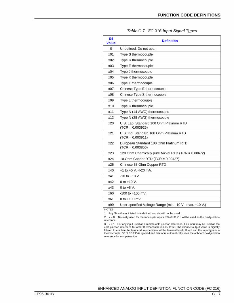
FUNCTION CODE DEFINITIONS
I-E96-301B
Table C-7. FC 216 Input Signal Types
S4 Value
Definition
0 Undefined. Do not use.
x01 Type S thermocouple
x02 Type R thermocouple
x03 Type E thermocouple
x04 Type J thermocouple
x05 Type K thermocouple
x06 Type T thermocouple
x07 Chinese Type E thermocouple
x08 Chinese Type S thermocouple
x09 Type L thermocouple
x10 Type U thermocouple
x11 Type N (14 AWG) thermocouple
x12 Type N (28 AWG) thermocouple
x20 U.S. Lab. Standard 100 Ohm Platinum RTD (TCR = 0.003926)
x21 U.S. Ind. Standard 100 Ohm Platinum RTD (TCR = 0.003911)
x22 European Standard 100 Ohm Platinum RTD (TCR = 0.003850)
x23 120 Ohm Chemically pure Nickel RTD (TCR = 0.00672)
x24 10 Ohm Copper RTD (TCR = 0.00427)
x25 Chinese 53 Ohm Copper RTD
x40 +1 to +5 V. 4-20 mA.
x41 -10 to +10 V.
x42 0 to +10 V.
x43 0 to +5 V.
x60 -100 to +100 mV.
x61 0 to +100 mV.
x99 User-specified Voltage Range (min. -10 V., max. +10 V.)NOTES:1. Any S4 value not listed is undefined and should not be used.2. x = 0 Normally used for thermocouple inputs. S3 of FC 215 will be used as the cold junctionreference.3. x = 1 For any input used as a remote cold junction reference. This input may be used as thecold junction reference for other thermocouple inputs. If x=1, the channel output value is digitallyfiltered to emulate the temperature coefficient of the terminal block. If x=1 and the input type is athermocouple, S3 of FC 215 is ignored and this input automatically uses the onboard cold junctionreference for compensation.
ENHANCED ANALOG INPUT DEFINITION FUNCTION CODE (FC 216)
C - 7

FUNCTION CODE DEFINITIONS ®
S5 This specification defines the temperature units displayed(degrees Celsius or Fahrenheit) if S4 indicates other than athermocouple or RTD type. Specification 5 is the type of engi-neering unit conversion to be performed on the input signal. IfS4 indicates a thermocouple or RTD type, then S5 is ignoredand S6/S7 are used to convert the input signal to engineeringunits.
S6 This specification defines the low limit of the input in engineer-ing units (EU). This value corresponds to the low end of theinput signal range as identified in S4. This specification isignored if the input type (S4) is a thermocouple or RTD.
S7 This specification defines the range of the input in engineeringunits. This value corresponds to the input signal range asidentified in S4. This specification is ignored if the input type(S4) is a thermocouple or RTD.
S8 This specification is ignored unless the input signal type (S4)indicates a user-specified voltage range. In that case, this spec-ification defines the lower limit of the range, in Volts.
S9 This specification is ignored unless the input signal type (S4)indicates a user-specified voltage range. In that case, this spec-ification defines the upper limit of the range, in Volts.
S10 This specification gives the resistance (in Ohms) of the fieldinput lead wire for this input coming into the terminationdevice. This value is used to correct the value of the input sig-nal. For millivolt and thermocouple inputs, lead wire resis-tance is the sum of the resistance in both the plus and minusleads. For three-wire RTD inputs, lead wire resistance is theresistance in any one of the three leads (the resistance of eachwire must be equal for accurate three-wire resistance measure-ments). This value is not used for high-level input types.
S11 The resolution of the analog-to-digital conversion may be spec-ified for each channel independently. This specification speci-fies the resolution as the number of bits in the binaryrepresentation of the raw input value when it is scanned by theslave module. A higher value for the resolution requires alonger conversion time and a correspondingly slower scanningrate for the inputs. Table C-8 lists the approximate resolutionand scan time relationship.
ENHANCED ANALOG INPUT DEFINITION FUNCTION CODE (FC 216)
C - 8 I-E96-301B
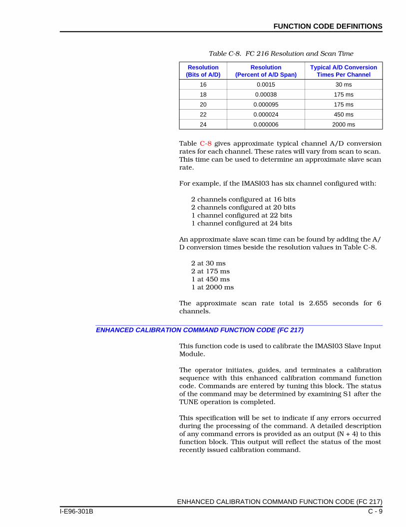
FUNCTION CODE DEFINITIONS
I-E96-301B
Table C-8 gives approximate typical channel A/D conversionrates for each channel. These rates will vary from scan to scan.This time can be used to determine an approximate slave scanrate.
For example, if the IMASI03 has six channel configured with:
2 channels configured at 16 bits2 channels configured at 20 bits1 channel configured at 22 bits1 channel configured at 24 bits
An approximate slave scan time can be found by adding the A/D conversion times beside the resolution values in Table C-8.
2 at 30 ms2 at 175 ms1 at 450 ms1 at 2000 ms
The approximate scan rate total is 2.655 seconds for 6channels.
ENHANCED CALIBRATION COMMAND FUNCTION CODE (FC 217)
This function code is used to calibrate the IMASI03 Slave InputModule.
The operator initiates, guides, and terminates a calibrationsequence with this enhanced calibration command functioncode. Commands are entered by tuning this block. The statusof the command may be determined by examining S1 after theTUNE operation is completed.
This specification will be set to indicate if any errors occurredduring the processing of the command. A detailed descriptionof any command errors is provided as an output (N + 4) to thisfunction block. This output will reflect the status of the mostrecently issued calibration command.
Table C-8. FC 216 Resolution and Scan Time
Resolution (Bits of A/D)
Resolution(Percent of A/D Span)
Typical A/D Conversion Times Per Channel
16 0.0015 30 ms
18 0.00038 175 ms
20 0.000095 175 ms
22 0.000024 450 ms
24 0.000006 2000 ms
ENHANCED CALIBRATION COMMAND FUNCTION CODE (FC 217)
C - 9
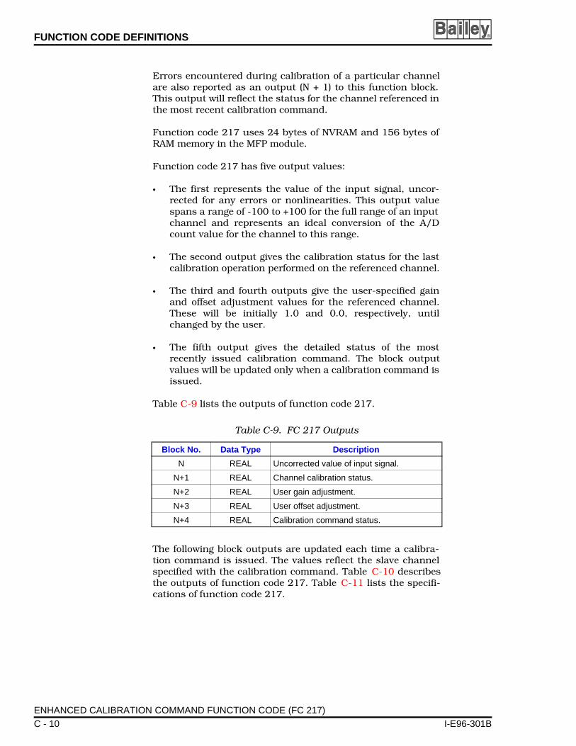
FUNCTION CODE DEFINITIONS ®
Errors encountered during calibration of a particular channelare also reported as an output (N + 1) to this function block.This output will reflect the status for the channel referenced inthe most recent calibration command.
Function code 217 uses 24 bytes of NVRAM and 156 bytes ofRAM memory in the MFP module.
Function code 217 has five output values:
• The first represents the value of the input signal, uncor-rected for any errors or nonlinearities. This output valuespans a range of -100 to +100 for the full range of an inputchannel and represents an ideal conversion of the A/Dcount value for the channel to this range.
• The second output gives the calibration status for the lastcalibration operation performed on the referenced channel.
• The third and fourth outputs give the user-specified gainand offset adjustment values for the referenced channel.These will be initially 1.0 and 0.0, respectively, untilchanged by the user.
• The fifth output gives the detailed status of the mostrecently issued calibration command. The block outputvalues will be updated only when a calibration command isissued.
Table C-9 lists the outputs of function code 217.
The following block outputs are updated each time a calibra-tion command is issued. The values reflect the slave channelspecified with the calibration command. Table C-10 describesthe outputs of function code 217. Table C-11 lists the specifi-cations of function code 217.
Table C-9. FC 217 Outputs
Block No. Data Type Description
N REAL Uncorrected value of input signal.
N+1 REAL Channel calibration status.
N+2 REAL User gain adjustment.
N+3 REAL User offset adjustment.
N+4 REAL Calibration command status.
ENHANCED CALIBRATION COMMAND FUNCTION CODE (FC 217)
C - 10 I-E96-301B

FUNCTION CODE DEFINITIONS
I-E96-301B
Table C-10. FC 217 Output Descriptions
Block No. Description
N Uncorrected value of input signal. This output gives the value of the input signal without any of the calibration, drift, lead wire, or cold junction compensations applied. The input value is converted to a range of -100 to +100 using an ideal conversion from the digitized value.
N+1 Channel calibration status. This output gives the detailed status of the last calibration operation performed on the specified channel.
0 - Channel calibration command was successful.1 - Channel reference error.2 - Out of range error.3 - Channel NOT calibrated error. (Applies if user attempts a
Set/Reset user parameters command to an uncalibrated channel type).
4 - NVRAM error.5 - A/D converter error.6 - Point NOT on curve error. (Measured values read during
calibration do NOT correspond linearly to the input valuesspecified by S5).
N+2 User gain adjustment. This output gives the value of the user specified gain adjustment. If none has been specified, this value will be 1.
N+3 User offset adjustment. This output gives the value of the user specified offset adjustment. If none has been specified, this value will be 0. The units for this value are Ohms for an RTD input or Volts otherwise.
N+4 This output represents the status of the most recently issued calibration command. Output information is organized in the format shown. Each decimal digit represents one type of status.
0 - Command parameters were specified correctly.1 - S1, Command code, not valid.2 - S2, Does not reference a valid IMASI03 function code 215 block.3 - S3, Channel number, not valid.4 - S4, Calibration type, calibration type invalid or not same as type
already in progress.5 - S5, Calibration point, not valid for type of input.
10 - Point not disabled.20 - Point already disabled.30 - Calibration point count error - must be more than one, less than
maximum allowed.40 - Factory calibration data is lost. Cannot process enable command.50 - Restore operation failed. Data was not successfully written into
field calibration data area.100 - Error occurred during channel calibration. Refer to N+1.
0000 - Slave responding normally, no errors.1000 - Slave not responding.2000 - Expander bus test failed.9999 - Calibration command processing.
ENHANCED CALIBRATION COMMAND FUNCTION CODE (FC 217)
C - 11

FUNCTION CODE DEFINITIONS ®
S1 This specification is tuned to the proper command code for thecalibration operation to be performed. S1 is returned as a zeroin the event of a calibration command error, and must bechanged before sending another calibration command to theslave. S1 is unchanged if calibration command processing issuccessful. The defined operations and their codes aredescribed here.
1 - Disable point. Removes a channel from normal input scanprocessing. A point must be disabled before any calibrationcan begin to prevent calibration related data from being inter-preted as process data by the rest of the system. Calibrationshould only be performed using precision voltage or resistancesources applied at the terminal blocks.
2 - Perform point calibration using external reference.
3 - Enable point. A point must be enabled before normal inputprocessing can occur. This action terminates the field calibra-tion sequence for a point. User gain and offset values will bereset to 1.0 and 0.0, respectively, if a successful calibrationhas been performed.
4 - Point Escape. The Point Escape command is used to reset(clear) calibration point information for a particular channel inthe middle of a calibration sequence. It clears only the pointdata. This allows the user to restart a calibration procedure forthe channel specified. The Point Escape command does notenable the channel.
5 - Set user gain and offset adjustment. This commandallows the user to enter a linear adjustment factor which willbe applied to the input signal after all drift and nonlinearitycorrections, but before conversion to engineering units. Thisvalue can be applied to low-level, high-level and resistancevalues.
Table C-11. FC 217 Specifications
Spec No.
TuneDefault Value
Data TypeRange
Min. MaxDescription
S1 Yes 0 INT(1) 0 to 255 Calibration operation code
S2 Yes 0 INT(2) 0 to 9998 Block Address of FC 215 used to configure the slave.
S3 Yes 0 INT(2) Full Slave channel number
S4 Yes 0 INT(1) 0 to 2 Calibration type
S5 Yes 0 REAL(3) Full Calibration parameter 1
S6 Yes 0 REAL(3) Full Calibration parameter 2
S7 No 0 INT(2) Full Spare
S8 No 0 REAL(3) Full Spare
ENHANCED CALIBRATION COMMAND FUNCTION CODE (FC 217)
C - 12 I-E96-301B

FUNCTION CODE DEFINITIONS
I-E96-301B
6 - Reset user gain and offset adjustment. This commandcancels any previously entered user gain and offset adjustmentfor the specified channel.
7 - Display uncorrected point data (percent of positive fullscale). This command performs no operation other than toupdate the uncorrected output data value for the specifiedinput channel (block output N of function code 217).
8 - Update point data. This command causes a new scan ofthe specified input channel to be performed and the outputdata value of the block to be updated with the new uncorrectedvalue.
9 - Slave escape command. Performs Point Escape commandto all 16 channels and cold junction reference on the IMASI03slave module.
10 - Expander bus test command. Performs single test ofexpander bus between MFP and slave. The test verifies trans-mission, reception and data integrity of messages passedbetween these modules. (Intended as an additional diagnosticfor the slave interface. It requires an MFP.)
11 - Restore factory calibration command. This commandoverwrites the field calibration data in NVRAM with the originalfactory calibration parameters. This command resets the val-ues entered in the set user gain and offset command.
S2 This specification identifies the block address of the enhancedanalog slave definition (function code 215) function block iden-tifying the slave module to which the command specified in S1is to be applied.
NOTE: For MFP01/02 firmware releases prior to C_0, S2 identifiesthe expander bus address of the slave module to which the com-mand specified in S1 is to be applied.
S3 This specification identifies the slave input channel number towhich the command specified in S1 is to be applied.
S4 This specification identifies which type of calibration is to beperformed.
0 = Low-level (millivolt, thermocouple)1 = High-level2 = RTD
S5 This specification is used for channel calibration and changingthe user gain and offset value. Calibration parameter 1 pro-vides a real value dependent upon the type of command speci-fied in S1.
ENHANCED CALIBRATION COMMAND FUNCTION CODE (FC 217)
C - 13
FUNCTION CODE DEFINITIONS ®
For command code 2, point calibration, this parameter speci-fies the true value of the signal applied to the input channelduring the calibration operation. Enter S5 for each calibrationpoint (twice if two points on a channel are calibrated). Up to 11points may be identified for adjustment of input channel non-linearities, resulting in 10 linear segments for correction.These calibration points may be applied in any order. The unitsfor the point value are determined by the type of calibrationoperation specified in S4.
For user gain and offset applications, S5 specifies the gain andS6 specifies the offset. When the IMASI03 is shipped, thedefault value for gain is set to one and the default value for off-set is set to zero. This command sets both the gain and offsetparameters simultaneously each time it is entered.
Example: Low-level = millivolts (-100.0 to +100.0)High-level = Volts (-10.0 to +10.0)RTD = Ohms (5.0 to 500)
For command code 5, user gain and offset adjustment, thisparameter specifies the gain, or slope, of the linear correctionto be applied. Both user gain and offset adjustment can bechanged at one time.
S6 Calibration parameter 2 provides a real value dependent uponthe type of command specified in S1.
For command code 5, user gain and offset adjustment, thisparameter specifies the offset, or intercept, of the linear correc-tion to be applied. The units for the offset value are determinedby the type of calibration operation specified in S4.
Example: Low-level = millivolts (-100.0 to +100.0)High-level = Volts (-10.0 to +10.0)RTD = Ohms (5.0 to 500)
S7-S8 Spare parameters.
ENHANCED CALIBRATION COMMAND FUNCTION CODE (FC 217)
C - 14 I-E96-301B

Index
A
Address Switch (SW1)................................................ 3-2Alarm and Exception Reporting......................... 2-10, 6-1All Tests Mode............................................................ 6-7Analog to Digital Conversion ...................................... 2-2Automatic Adjustments and Corrections
Automatic Calibration............................................ 2-9Cold Junction Compensation................................ 2-7Engineering Units Conversion .............................. 2-8Input Calibration.................................................... 2-7Input Processing................................................... 2-6Lead Wire Resistance........................................... 2-7Point Value Calculation......................................... 2-6User Gain and Offset ............................................ 2-8
Automatic Calibration ................................................. 2-9
B
Binary Slave Address ................................................. 3-3Block Diagram ............................................................ 2-1Bus Connections ........................................................ 6-9
C
Cable Connections ..................................................... 3-6Cable Connections, NIAI05 to IMASI03 ..................... 3-6Cable Connections, NTAI06 to IMASI03 .................... 3-7Calculating Point Values ............................................ 2-6Calibrating Inputs ................................................ 2-7, 4-2Calibration, Automatic ................................................ 2-9Calibration, Field ................................................. 2-9, 4-3Channel Calibration, Individual................................... 4-6Channel Data ............................................................. 6-2Cold Junction Compensation ..................................... 2-7Cold Junction Reference ............................................ 2-3Configuration Function Codes.................................... 4-1Configuration, On-Line ............................................. 2-11Configuring Inputs ............................................... 3-3, 4-1
Function Codes, Configuration ............................. 4-1Input Calibration.................................................... 2-9
Connections, Input ..................................................... 6-9Connections, Output................................................... 6-9Connectors P1, P2, P3............................................... 3-5Continue - Do Not Display Error ................................. 6-6Corrective Actions for Error Messages....................... 6-2
D
Data on Input Channels ..............................................6-2Data Values ................................................................2-5Diagnostics .................................................................6-7Diagnostics Run During Normal Operation...............2-10Diagnostics Run in Diagnostic Mode ........................2-10Diagnostics Run on Reset ..........................................2-9Dipswitch Test.............................................................6-7Documentation............................................................9-1
E
Engineering Units Conversion ....................................2-8Error Codes and SW1 Settings...................................6-6Error Messages and Actions.......................................6-2Error on Master Module ..............................................6-2Exception and Alarm Reporting ..................................6-1Expander Bus Communication Security ...................2-10Expander Bus Interface ..............................................2-5
F
Field Calibration ...................................................2-9, 4-3Calibration Instruction ...........................................4-5Calibration Ranges................................................4-4Calibration Steps...................................................4-4Function Code 217................................................4-3Individual Channel Calibration ..............................4-6Test Equipment Required .....................................4-6
Function Code 215......................................................4-1Function Code 216......................................................4-1Function Code 217......................................................4-3Function Codes...........................................................2-5Function Codes, Configuration ...................................4-1Functional Operation
Analog to Digital Conversion.................................2-2Input Multiplexer (MUX) ........................................2-2Isolation Amplifier..................................................2-2Microcontroller and Memory..................................2-3On-Board Indicators ..............................................2-4Slave Expander Bus..............................................2-4Slave Expander Bus Interface...............................2-5Switch Settings......................................................2-4Termination Units ..................................................2-5
I-E96-301B Index - 1
Index (continued)
®
G
Gain and Offset Adjustment ........................................2-8Glossary of Terms and Abbreviations.........................1-5
H
Halt - Display Error......................................................6-5
I
IMASI03Block Diagram.......................................................2-1Description of Module............................................1-1Documentation ......................................................9-1Features ................................................................1-2Functional Operation .............................................2-1INFI 90 Communication Levels ......................1-2, 2-2Input Calibration ....................................................2-9Inspection ..............................................................3-1Installation .............................................................3-2Logic Power.........................................................2-11Maintenance Schedule..........................................7-1Module Description................................................1-1On-Board Indicators ............................... 2-4, 5-1, 6-1On-Line Configuration .........................................2-11Operating Procedures ............................ 5-1, 6-1, 7-1Operation...............................................................5-1Ordering Parts .......................................................9-1Overview ...............................................................1-1Setup.....................................................................3-2Slave Expander Bus..............................................2-4Slave Expander Bus Interface...............................2-5Start-Up .................................................................5-1Switch Settings......................................................2-4Termination Units ..................................................2-5Training .................................................................9-1Troubleshooting..............................................6-1, 7-1Unpacking .............................................................3-1
IMASI03 to NIAI05 Cable Connections.......................3-6IMASI03 to NTAI06 Cable Connections......................3-7Input Calibration...................................................2-7, 2-9Input Channel Data .....................................................6-2Input Connections .......................................................6-9Input Multiplexer (MUX) ..............................................2-2Input Processing .........................................................2-6Inputs, Calibrating .......................................................4-2
Inputs, Configuring the ............................................... 4-1Isolation Amplifier ....................................................... 2-2
J
Jumper Configuration ................................................. 3-4Jumper Location ......................................................... 3-4Jumpers Used for Each Channel................................ 3-4
L
Lead Wire Resistance ................................................ 2-7Logic Power.............................................................. 2-11
M
Maintenance Schedule ............................................... 7-1Manual
Glossary of Terms and Abbreviations................... 1-5How to Use This Manual....................................... 1-4Instruction Content................................................ 1-4Intended User ....................................................... 1-1Nomenclature ....................................................... 1-7Specifications................................................. 1-8, 1-9
Master Module Errors ................................................. 6-2Memory....................................................................... 2-3Memory and Microcontroller ....................................... 2-3Microcontroller ............................................................ 2-3Microcontroller and Memory ....................................... 2-3Module Description..................................................... 1-1Module Functional Tests
All Tests Mode ...................................................... 6-7Continue - Do Not Display Error ........................... 6-6Diagnostics ........................................................... 6-7Dipswitch Test ...................................................... 6-7Halt-Display Error ................................................. 6-5Module Functional Test ........................................ 6-5Slave Expander Bus Test ..................................... 6-8Test Equipment Required ..................................... 6-5
Module Inspection ...................................................... 3-1Module Installation...................................................... 3-2Module Jumpers ......................................................... 3-4Module Repair/Replacement Procedures................... 8-1Module Setup ............................................................. 3-2Module Unpacking...................................................... 3-1Module Wiring............................................................. 3-6
Index - 2 I-E96-301B

Index (continued)
N
NIAI05 to IMASI03 Cable Connections ...................... 3-6Nomenclature ............................................................. 1-7NTAI06 to IMASI03 Cable Connections ..................... 3-7
O
Offset and Gain Adjustment ....................................... 2-8On-Board Indicators ..................................... 2-4, 5-1, 6-1On-Line Configuration .............................................. 2-11Open Input Detection ............................................... 2-10Operating Modes........................................................ 6-6Operating Procedures .................................. 5-1, 6-1, 7-1Operation.................................................................... 5-1Ordering Information .................................................. 9-1Output Connections.................................................... 6-9
P
P1, P2, P3 Connectors ............................................... 3-5Parts Ordering Information ......................................... 9-1Point Value Calculation .............................................. 2-6Power Connections .................................................... 6-9Power, Logic............................................................. 2-11Processing Slave Inputs............................................. 2-6
R
Reference Documents................................................ 1-7Repair/Replacement Procedures ............................... 8-1Replacement Parts ..................................................... 9-1Replacement Parts and Ordering Information............ 9-1Replacement/Repair Procedures ............................... 8-1
S
Security and Integrity ChecksAlarm and Exception Reporting.......................... 2-10Diagnostics Run During Normal Operation......... 2-10Diagnostics Run in Diagnostic Mode.................. 2-10Diagnostics Run on Reset .................................... 2-9Expander Bus Communication Security ............. 2-10Open Input Detection.......................................... 2-10
Select Slave Address ................................................. 3-2Setup and Installation
Address Switch (SW1).......................................... 3-2
Binary Slave Address............................................3-3Configuring Inputs .................................................3-3Jumper Configuration............................................3-4Jumper Location....................................................3-4Jumpers Used for Each Channel ..........................3-4Physical Installation...............................................3-5Termination Module/Unit Configuration.................3-5
Slave Expander Bus ...................................................2-4Slave Expander Bus Connections ..............................6-9Slave Expander Bus Interface ....................................2-5Slave Expander Bus Interface Test ............................6-8Slave Power Connections...........................................6-9Special handling..........................................................3-1Specifications.......................................................1-8, 1-9Start-Up.......................................................................5-1Support Services.........................................................9-1SW1 Address switch ...................................................3-2SW1 Settings and Error Codes...................................6-6Switch Settings ...........................................................2-4
T
Technical Documentation ...........................................9-1Termination Cable Connections..................................3-6Termination Module/Unit Configuration ......................3-5Termination Units........................................................2-5Test Equipment Required ...........................................6-5Training .......................................................................9-1Troubleshooting ...................................................6-1, 7-1
On-Board Indicators ..............................................2-4SW1 Settings and Error Codes .............................6-6
U
Universal Slave Bus Interface Test.............................6-8User Gain and Offset ..................................................2-8
W
Wiring..........................................................................3-6Wiring Connections and Cabling
Cable Connections................................................3-6IMASI03 to NIAI05 ................................................3-6IMASI03 to NTAI06 ...............................................3-7P1, P2, P3 .............................................................3-5
I-E96-301B Index - 3

Visit Elsag Bailey on the World Wide Web at http://www.bailey.com
Our worldwide staff of professionals is ready to meet your needs for process automation. For the location nearest you, please contact the appropriate regional office.
AMERICAS29801 Euclid AvenueWickliffe, Ohio USA 44092Telephone 1-216-585-8500Telefax 1-216-585-8756
ASIA/PACIFIC152 Beach RoadGateway East #20-04Singapore 189721Telephone 65-391-0800Telefax 65-292-9011
EUROPE, AFRICA, MIDDLE EASTVia Puccini 216154 Genoa, ItalyTelephone 39-10-6582-943Telefax 39-10-6582-941
GERMANYGraefstrasse 97D-60487 Frankfurt MainGermanyTelephone 49-69-799-0Telefax 49-69-799-2406
Form I-E96-301B1 Litho in U.S.A. 1294Copyright © 1994 by Elsag Bailey Process Automation, As An Unpublished Work® Registered Trademark of Elsag Bailey Process Automation™ Trademark of Elsag Bailey Process Automation


