ECC Handling in TMSx70-Based MicrocontrollersFrank Noha ....................................................................................................................................
ABSTRACT
This application report describes the Flash and RAM ECC handling methods for TMSx70-basedmicrocontrollers in general.
To use the Flash/RAM ECC, the single error correction and double error detection (SECDED) module inthe TMSx70 has to be configured accordingly. This application report covers typical softwareconfigurations of the SECDED modules and briefly explains some essential basics.
NOTE: To see if Flash ECC or RAM ECC is supported for your microcontroller and the respectiveFlash wrapper specification for technical details, see the TMSx70 device-specific data sheet.
Contents1 Error Detection and Correction Techniques ............................................................................. 22 Flash With ECC ............................................................................................................. 83 RAM With ECC ............................................................................................................ 154 References ................................................................................................................. 19Appendix A Terminology ....................................................................................................... 20
List of Figures
1 SECDED Block Diagram of Typical Flash Wrapper .................................................................... 3
2 SECDED Block Diagram of a Typical RAM Wrapper .................................................................. 4
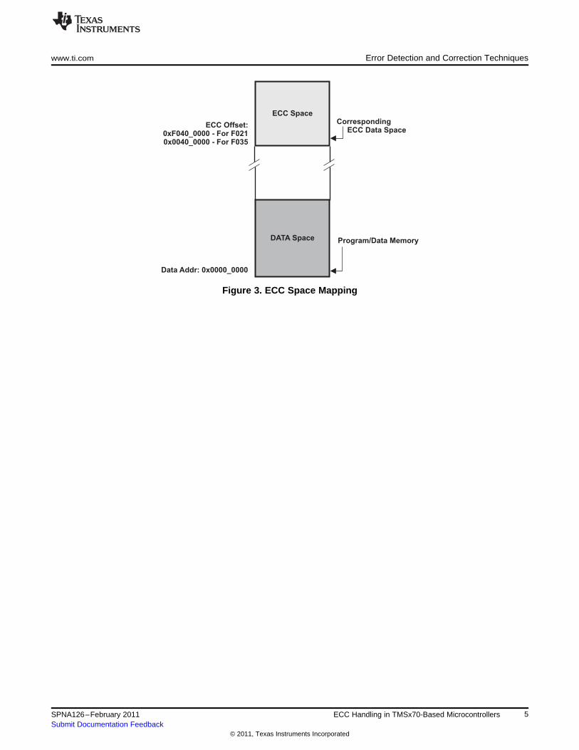
3 ECC Space Mapping ....................................................................................................... 5
4 Data and ECC Space Mapping for F035 Flash in TMSx70 ........................................................... 8
5 Data and ECC Space Mapping for F021 Flash in TMSx70 ........................................................... 9
Error Detection and Correction Techniques www.ti.com
1 Error Detection and Correction Techniques
In microcontrollers, the data stored in the memory could get corrupted over a period of time due to severalreasons. This creates a necessity for the system to verify the correctness of the data before or whileexecuting the software in the memory. The Error detection techniques help the system to check theintegrity of the data in the memory.
Parity - This technique requires additional bits to be added corresponding to the data. Parity only detectssingle bit failures in a memory. This is a simpler well known error detection technique.
ECC - Adding Error Correcting Code (ECC) bits along with the original data is a technique that helps indetecting errors as well as correcting errors. The ECC scheme used on the TMSx70 devices is able todetect up to 2-bit failures and correct single bit failures.
The implementation and behavior of these error detection schemes makes it necessary for you tounderstand certain restrictions when using them in the application or while debugging the system. Thisapplication report covers only the ECC technique for TMSx70-based microcontrollers.
NOTE: Refer to the TMSx70 microcontroller-specific data sheet to know the kind of error detectiontechnique supported.
1.1 Single Error Correction and Double Error Detection (SECDED)
SECDED is the hardware module embedded in the Flash/RAM wrapper that generates ECC, compares,detects the error bits and corrects if it is a single bit error.
• SECDED is capable of correcting single bit errors and detecting multiple bit errors.• SECDED requires a total of eight ECC check bits associated with each 64-bit wide data word and its
corresponding address.• SECDED is adapted based on Flash/RAM technology design of the controller. Some designs have two
SECDED modules that operate in parallel the results of which are compared and accepted only if bothare same.
The SECDED logic in the respective memory wrapper calculates and checks the ECC bits in the TMSx70microcontrollers. The logic is different for different memory types and CPUs.
1.1.1 TMSx70 Memory Types• Flash – F021, F035
– In case of Flash, the corresponding ECC values have to be programmed along with the data(program). The logic is adapted according to the corresponding flash technology of themicrocontroller. Refer to the microcontroller specific datasheet to know more technical details of theSECDED module and ECC space mapping. (1)
• RAM – TCRAM, ESRAM– In case of RAM, the hardware generates the corresponding ECC check bits for the data during a
write operation and stores them in the respective ECC memory location. During a memory read, theECC bits in the ECC space are read along with the data to detect or correct any error.The RAM wrapper implementation is based on the CPU type.
1.1.2 TMSx70 CPU Types
The TMSx70 microcontrollers may be of any of the following CPU types from ARM®.
• ARM7TDMI®
• Cortex™-M3• Cortex-R4
(1) nowECC™ is a TI proprietary tool.nowECC, nowFlash are trademarks of Texas Instruments.Cortex is a trademark of ARM Limited.ARM, ARM7TDMI are registered trademarks of ARM Limited.All other trademarks are the property of their respective owners.
2 ECC Handling in TMSx70-Based Microcontrollers SPNA126–February 2011Submit Documentation Feedback
www.ti.com Error Detection and Correction Techniques
In case of Cortex-R4 based CPU, the ECC encoding/decoding is done by the CPU (in-built), whereas,in case of Cortex-M3 and ARM7TDMI-based CPUs, the ECC encoding/decoding is done by the RAMwrapper. The main advantage of having the encoding/decoding within the CPU is to speed up theaccesses by removing the time consuming SECDED block.
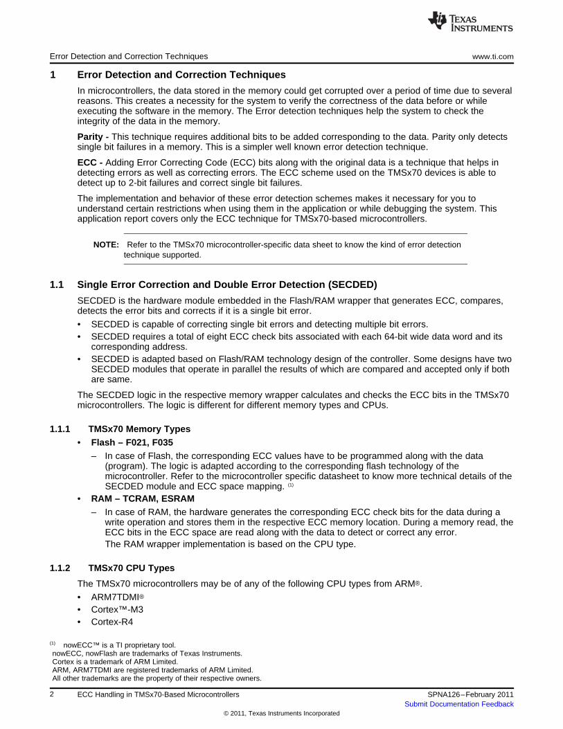
1.2 Flash Wrapper With ECC
You have to generate the ECC for the data and program it into the ECC space before enabling the ECC.
During the read operation, the 64-bit data together with the 19 address bits (21:3) pass through the ECCgenerator to produce the 8 check bits. These eight calculated ECC check bits are then XOR'ed with thestored check bits associated with the address and the read data. The 8-bit output is the syndrome.
For more information on mathematical ECC check bit calculation, see Section 1.5.
Figure 1. SECDED Block Diagram of Typical Flash Wrapper
The syndrome is decoded to determine one of three conditions:
• No error occurred.• A correctable error occurred.• A non-correctable error occurred.
NOTE: A single bit error in the address field is considered to be a non-correctable error.
3SPNA126–February 2011 ECC Handling in TMSx70-Based MicrocontrollersSubmit Documentation Feedback
Error Detection and Correction Techniques www.ti.com
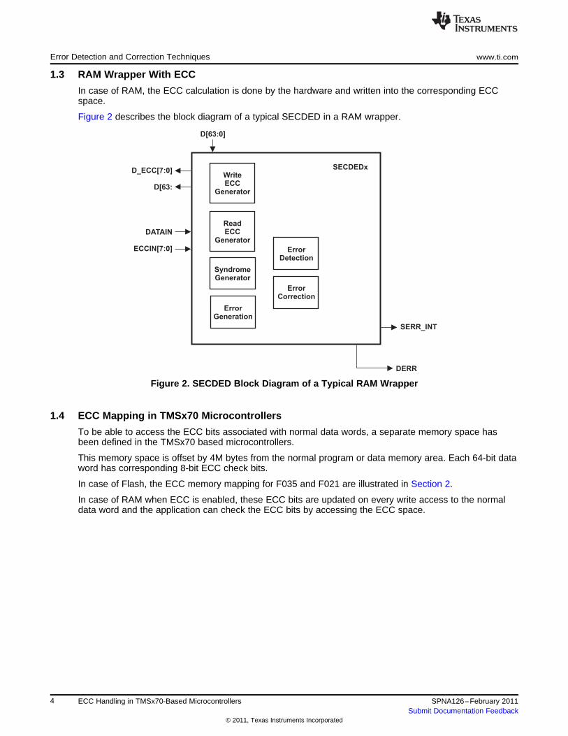
1.3 RAM Wrapper With ECC
In case of RAM, the ECC calculation is done by the hardware and written into the corresponding ECCspace.
Figure 2 describes the block diagram of a typical SECDED in a RAM wrapper.
Figure 2. SECDED Block Diagram of a Typical RAM Wrapper
1.4 ECC Mapping in TMSx70 Microcontrollers
To be able to access the ECC bits associated with normal data words, a separate memory space hasbeen defined in the TMSx70 based microcontrollers.
This memory space is offset by 4M bytes from the normal program or data memory area. Each 64-bit dataword has corresponding 8-bit ECC check bits.
In case of Flash, the ECC memory mapping for F035 and F021 are illustrated in Section 2.
In case of RAM when ECC is enabled, these ECC bits are updated on every write access to the normaldata word and the application can check the ECC bits by accessing the ECC space.
4 ECC Handling in TMSx70-Based Microcontrollers SPNA126–February 2011Submit Documentation Feedback
Error Detection and Correction Techniques www.ti.com
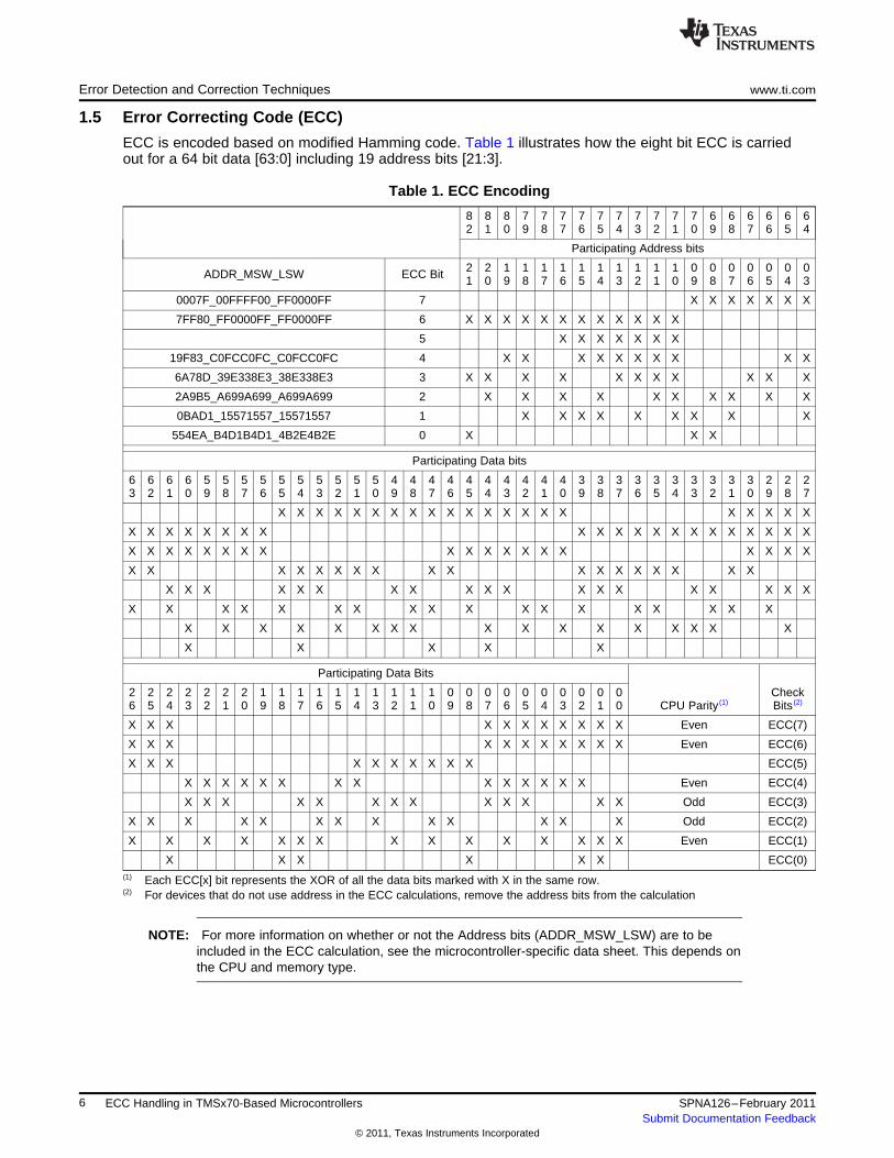
1.5 Error Correcting Code (ECC)
ECC is encoded based on modified Hamming code. Table 1 illustrates how the eight bit ECC is carriedout for a 64 bit data [63:0] including 19 address bits [21:3].
X X X X X X ECC(0)(1) Each ECC[x] bit represents the XOR of all the data bits marked with X in the same row.(2) For devices that do not use address in the ECC calculations, remove the address bits from the calculation
NOTE: For more information on whether or not the Address bits (ADDR_MSW_LSW) are to beincluded in the ECC calculation, see the microcontroller-specific data sheet. This depends onthe CPU and memory type.
6 ECC Handling in TMSx70-Based Microcontrollers SPNA126–February 2011Submit Documentation Feedback
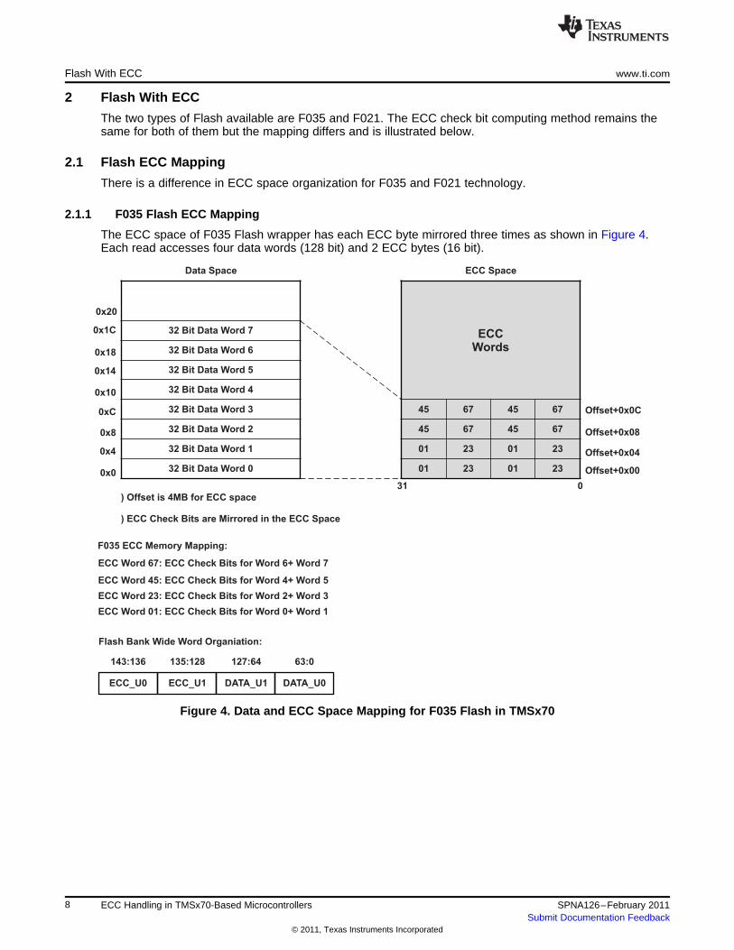
The two types of Flash available are F035 and F021. The ECC check bit computing method remains thesame for both of them but the mapping differs and is illustrated below.
2.1 Flash ECC Mapping
There is a difference in ECC space organization for F035 and F021 technology.
2.1.1 F035 Flash ECC Mapping
The ECC space of F035 Flash wrapper has each ECC byte mirrored three times as shown in Figure 4.Each read accesses four data words (128 bit) and 2 ECC bytes (16 bit).
Figure 4. Data and ECC Space Mapping for F035 Flash in TMSx70
8 ECC Handling in TMSx70-Based Microcontrollers SPNA126–February 2011Submit Documentation Feedback
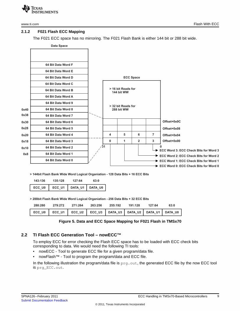
> 144bit Flash Bank Wide Word Logical Organiation - 128 Data Bits + 16 ECC Bits
288:280
ECC_U0
279:272
ECC_U1
271:264
ECC_U2
263:256
ECC_U3
> 288bit Flash Bank Wide Word Logical Organiation - 256 Data Bits + 32 ECC Bits
255:192
DATA_U3
191:128
DATA_U2
127:64
DATA_U1
63:0
DATA_U0
> 16 bit Reads for144 bit WW
> 32 bit Reads for288 bit WW
www.ti.com Flash With ECC
2.1.2 F021 Flash ECC Mapping
The F021 ECC space has no mirroring. The F021 Flash Bank is either 144 bit or 288 bit wide.
Figure 5. Data and ECC Space Mapping for F021 Flash in TMSx70
2.2 TI Flash ECC Generation Tool – nowECC™
To employ ECC for error checking the Flash ECC space has to be loaded with ECC check bitscorresponding to data. We would need the following TI tools:• nowECC - Tool to generate ECC file for a given program/data file.• nowFlash™ - Tool to program the program/data and ECC file.
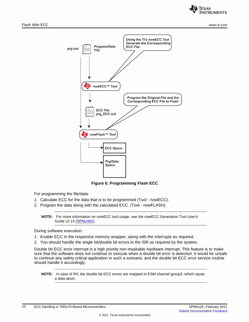
In the following illustration the program/data file is prg.out, the generated ECC file by the now ECC toolis prg_ECC.out.
9SPNA126–February 2011 ECC Handling in TMSx70-Based MicrocontrollersSubmit Documentation Feedback
Using the TI’s nowECC ToolGenerate the CorrespondingECC File.
Program the Original File and theCorresponding ECC File to Flash
prg.outProgram/DataFile
ECC Fileprg_ECC.out
¥
¥
ECC Space
Prg/DataSpace
Flash With ECC www.ti.com
Figure 6. Programming Flash ECC
For programming the file/data:
1. Calculate ECC for the data that is to be programmed (Tool - nowECC).2. Program the data along with the calculated ECC. (Tool - nowFLASH).
NOTE: For more information on nowECC tool usage, see the nowECC Generation Tool User'sGuide v2.14 (SPNU491).
During software execution:
1. Enable ECC in the respective memory wrapper, along with the interrupts as required.2. You should handle the single bit/double bit errors in the ISR as required by the system.
Double bit ECC error interrupt is a high priority non-maskable hardware interrupt. This feature is to makesure that the software does not continue to execute when a double bit error is detected. It would be unsafeto continue any safety critical application in such a scenario, and the double bit ECC error service routineshould handle it accordingly.
NOTE: In case of R4, the double bit ECC errors are mapped to ESM channel group3, which causea data abort.
10 ECC Handling in TMSx70-Based Microcontrollers SPNA126–February 2011Submit Documentation Feedback
The following describes the general algorithm to be followed to enable or disable the ECC check:
1. Make sure that the ECC section is programmed before enabling the ECC.2. Enable/disable single error correction/detection.3. Enable/disable appropriate error interrupts.4. Enable ECC/SECDED. (1)
5. In case of ECC error interrupts, handle it in the ISRs.
The ECC (SECDED) is globally enabled or disabled by a 4-bit EDACEN register. The ECC logic isdisabled when the four bits are 0101. Any non-0101 combination value stored in the EDACEN registerenables the ECC logic. It is advised to enable the ECC logic with 0xA value stored in the EDACEN toprevent any soft error from disabling the logic.
Instructions to enable ECC for M3- and ARM7-based CPUs:
In case of controllers with R4 CPU, the ECC check logic is within the CPU; this needs to be enabled afterenabling the ECC in the Flash wrapper. Enabling the Flash wrapper ECC would keep the status registersin the Flash wrapper updated.
NOTE: In case of Cortex-R4, it is recommended to flush the internal buffers using the DMB and ISBinstructions after enabling/disabling the ECC and before reading/writing further data.
2.4 Debugging With ECC Enabled
The following ECC status registers should be monitored by the application software during an event ofoccurrence of an ECC error:
• Error Status Register [ FEDACSTATUS]
– One Fail Status Flag - Indicates error on one fail– Zero Fail Status Flag - Indicates error on zero fail– Multiple Bit Error Status Flag - Indicates multiple errors
• Correctable Error Address Register [FCOR_ERR_ADD ] - Indicates corrected error bit address• Uncorrectable Error Address Register FUNC_ERR_ADD - Indicates double bit error address• Correctable Error Position Register - Indicates corrected error position
During error profiling the following registers are used.
• Single Error Correction Threshold Register - To program the threshold value.• Error Correction Counter Register - Indicates number of times a correctable error occurred.
2.4.1 Single Stepping On Single/Multiple Bit Error
By single stepping with the debugger, you can simulate and verify single/multiple bit error scenarios.
With the Flash ECC and the ECC error interrupts enabled, when you try to single step using the debuggerand encounters a single/multiple bit error, an error interrupt is generated by the hardware.
For single-bit error, the error bit will be corrected when read/executed by the CPU and you can continuewith the code execution after clearing the relevant flags in the service routine.
For multiple-bit error, you may have to take appropriate steps depending on the application. Since theerror cannot be corrected, continuing to execute the code would not be safe.
NOTE: In case of Cortex-R4, single stepping with ECC enabled will result in an abort.
12 ECC Handling in TMSx70-Based Microcontrollers SPNA126–February 2011Submit Documentation Feedback
Perform any Operation asRequired by the Application.
Module Ready to CaptureFurther ECC Errors.
www.ti.com Flash With ECC
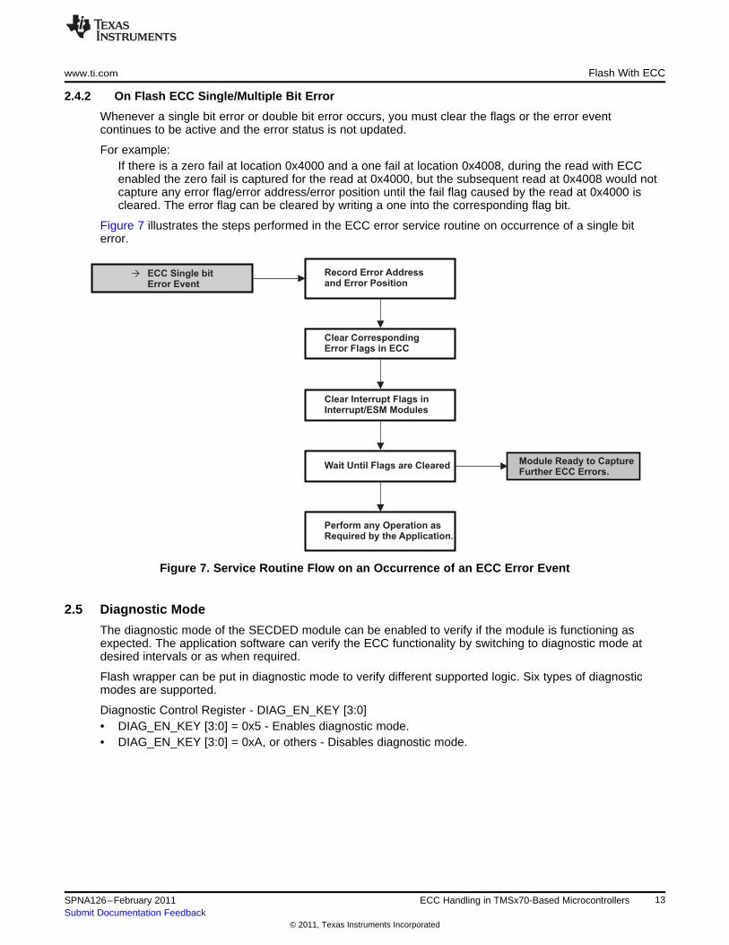
2.4.2 On Flash ECC Single/Multiple Bit Error
Whenever a single bit error or double bit error occurs, you must clear the flags or the error eventcontinues to be active and the error status is not updated.
For example:If there is a zero fail at location 0x4000 and a one fail at location 0x4008, during the read with ECCenabled the zero fail is captured for the read at 0x4000, but the subsequent read at 0x4008 would notcapture any error flag/error address/error position until the fail flag caused by the read at 0x4000 iscleared. The error flag can be cleared by writing a one into the corresponding flag bit.
Figure 7 illustrates the steps performed in the ECC error service routine on occurrence of a single biterror.
Figure 7. Service Routine Flow on an Occurrence of an ECC Error Event
2.5 Diagnostic Mode
The diagnostic mode of the SECDED module can be enabled to verify if the module is functioning asexpected. The application software can verify the ECC functionality by switching to diagnostic mode atdesired intervals or as when required.
Flash wrapper can be put in diagnostic mode to verify different supported logic. Six types of diagnosticmodes are supported.
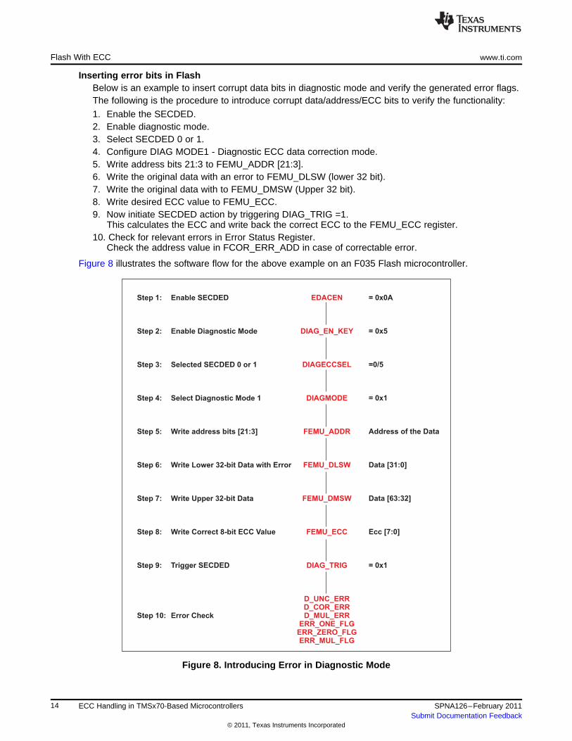
Inserting error bits in FlashBelow is an example to insert corrupt data bits in diagnostic mode and verify the generated error flags.The following is the procedure to introduce corrupt data/address/ECC bits to verify the functionality:
1. Enable the SECDED.2. Enable diagnostic mode.3. Select SECDED 0 or 1.4. Configure DIAG MODE1 - Diagnostic ECC data correction mode.5. Write address bits 21:3 to FEMU_ADDR [21:3].6. Write the original data with an error to FEMU_DLSW (lower 32 bit).7. Write the original data with to FEMU_DMSW (Upper 32 bit).8. Write desired ECC value to FEMU_ECC.9. Now initiate SECDED action by triggering DIAG_TRIG =1.
This calculates the ECC and write back the correct ECC to the FEMU_ECC register.10. Check for relevant errors in Error Status Register.
Check the address value in FCOR_ERR_ADD in case of correctable error.
Figure 8 illustrates the software flow for the above example on an F035 Flash microcontroller.
Figure 8. Introducing Error in Diagnostic Mode
14 ECC Handling in TMSx70-Based Microcontrollers SPNA126–February 2011Submit Documentation Feedback
The two types of RAM available are TCRAM wrapper and ESRAM wrapper. The TCRAM wrapper isspecific to Cortex-R4 CPU type whereas ESRAM is for Cortex-M3 CPU type. The ECC check bitcomputation method remains the same for both.
3.1 Initializing RAM and ECC
In the case of RAM with ECC, when the device comes out of reset the data and ECC memory is in anunknown state. If ECC is enabled, any write access less than 64 bits forces a read-modify-write operationto calculate the correct ECC bits for the corresponding 64-bit data word. This read-modify-write most likelyresults in a false double bit error.
To avoid these false double bit errors, you must initialize RAM and its ECC space before enabling theECC. You can do this by either of the following two methods.
3.1.1 Initialization Using Software
By enabling the Read-modify-write bypass (RMWCBYP) bit in the RAM Control register (RAMCTRL) thefalse double bit errors can be avoided. This bypasses the ECC checking while loading the data. With ECCenabled, the SECDED calculates and loads the corresponding ECC in the ECC space. After loading iscomplete, you should disable the RMWCBYP bit.
In order to avoid false errors after power up and to efficiently initialize the RAM to a know state, the RAMwrapper has the capability to initialize the entire RAM array to a known state by writing all zeros to thedata bits. If RAM ECC is enabled, the corresponding ECC check bits are also calculated and written to theECC bits. After the initialization of RAM and RAM ECC, you need to make sure that the initialization iscomplete before making the first RAM write.
– Captures the error address when detecting a double bit error.
3.2.1 Single Stepping On Single/Multiple Bit Error
With the RAM ECC enabled, when you try to single step using the debugger and encounter asingle/multiple bit error, no error interrupts will be generated by the hardware even if the interrupts areenabled by the application software. Although the single error correction will happen when the word withthe error bit is read by the CPU.
This is because when you execute from RAM and try to single step or add a software breakpoint, it wouldintroduce unintended error interrupts, since the software breakpoints will change the opcodes at thoseaddresses. These error interrupts are blocked by the hardware only while single stepping, so that thedebug flow is not affected.
In case of Cortex-R4, single stepping with ECC on results in an abort.
3.2.2 On RAM ECC Single/Multiple Bit Error
Whenever a single bit error or a double bit error occurs, you must clear the flags or the error eventcontinues to be active and the error status is not updated.
3.3 Disabling/Enabling ECC During Run Time
It is recommended to either use the ECC or not, throughout the application; however, you must be carefulwhen disabling or enabling the ECC in between program executions. Also, there might be a scenariowhere the ECC may have to be disabled and then re-enabled for a specific task, or while accessing aspecific location during run time.
While enabling or disabling the ECC you need to make sure that the ECC enable/disable is completebefore any next write/read instructions are executed.
For example, if a specific section of data does not have its ECC programmed, you should disable ECCwhile accessing those locations.
3.3.1 Steps to Enable ECC1. Enable ECC.2. Wait until ECC enable instruction is complete.
Instructions to enable ECC for M3- and ARM7-based CPUs:
ECC_Ptr->RAMCTRL_UN.RAMCTRL_ST.ECC_ENABLE_B4 = 0xA; /* enable ECC */ECC_Ptr->RAMCTRL_UN.RAMCTRL_ST.ECC_ENABLE_B4; /* wait for write to complete */
To enable ECC for R4-based CPUs:
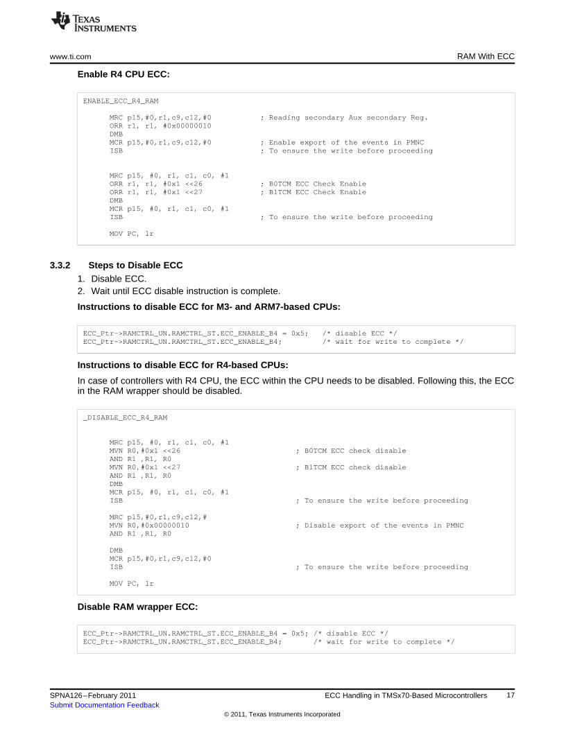
In case of controllers with R4 CPU, the ECC generation logic is within the CPU and this needs to beenabled. The ECC in the RAM wrapper should also be enabled before enabling the ECC in R4, this wouldkeep the status registers in the RAM wrapper updated.
ECC_Ptr->RAMCTRL_UN.RAMCTRL_ST.ECC_ENABLE_B4 = 0xA; /* enable ECC */ECC_Ptr->RAMCTRL_UN.RAMCTRL_ST.ECC_ENABLE_B4; /* wait for write to complete */
16 ECC Handling in TMSx70-Based Microcontrollers SPNA126–February 2011Submit Documentation Feedback
MRC p15,#0,r1,c9,c12,#0 ; Reading secondary Aux secondary Reg.ORR r1, r1, #0x00000010DMBMCR p15,#0,r1,c9,c12,#0 ; Enable export of the events in PMNCISB ; To ensure the write before proceeding
To check the ECC functionality of the RAM ECC, error can be introduced by the application software atknown locations and verified.
The following steps can be followed to introduce an ECC error into the RAM and to check if the RAM logicis working as expected.
Steps to introduce an error:
1. Initialize RAM – As mentioned in Section 3.1.2. Enable ECC – This switches on the ECC generation logic.3. Write data to a specific RAM location – This generates and loads the corresponding ECC check bits.4. Disable ECC – This switches off the ECC generation logic so as to enable you to corrupt data.5. Wait until ECC disabled – Although this step is not mandatory, make sure that it flushes the buffers.6. Change only the data (Flip one bit) – This corrupts only the data part.7. Enable ECC error interrupt – This enables you to handle the error in the exception routine.8. Enable ECC – This switches on the ECC generation logic again and creates a scenario to check the
logic.9. Read the corrupted data. – The logic performs an ECC check when you read the same data.10. Check for single bit error event – The ECC logic should generate a single bit error.
This flow can be used by the application at required intervals to check that the RAM ECC logic worksfine.
3.5 Switching Between ECC and EDC Modes
ECC Mode and EDC mode:
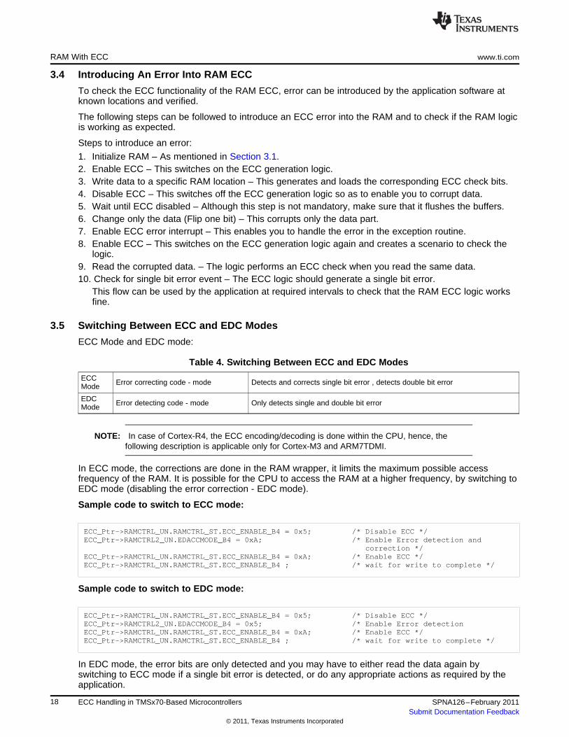
Table 4. Switching Between ECC and EDC Modes
ECC Error correcting code - mode Detects and corrects single bit error , detects double bit errorMode
EDC Error detecting code - mode Only detects single and double bit errorMode
NOTE: In case of Cortex-R4, the ECC encoding/decoding is done within the CPU, hence, thefollowing description is applicable only for Cortex-M3 and ARM7TDMI.
In ECC mode, the corrections are done in the RAM wrapper, it limits the maximum possible accessfrequency of the RAM. It is possible for the CPU to access the RAM at a higher frequency, by switching toEDC mode (disabling the error correction - EDC mode).
In EDC mode, the error bits are only detected and you may have to either read the data again byswitching to ECC mode if a single bit error is detected, or do any appropriate actions as required by theapplication.
18 ECC Handling in TMSx70-Based Microcontrollers SPNA126–February 2011Submit Documentation Feedback
At higher frequencies, you can operate in ECC mode with additional RAM wait states.
Sample code to enable RAM data wait states:
SYS_Ptr->WAITST_UN.WAITST_ST/WST_DEN_B1=0x1; /* Enable RAM data wait-state */
The requirement of data wait states for higher frequencies is device specific.
Also note that in the ARM7 or the Cortex M3 CPU based microcontrollers, the ECC correction is done inthe RAM wrapper. In the Cortex-R4 CPU-based devices, the ECC correction is done by the CPU itself.
NOTE: For more information on the supported clock frequency to operate RAM with ECC and waitstates required to operate at higher frequencies, see the device-specific data sheet .
Texas Instruments Incorporated and its subsidiaries (TI) reserve the right to make corrections, modifications, enhancements, improvements,and other changes to its products and services at any time and to discontinue any product or service without notice. Customers shouldobtain the latest relevant information before placing orders and should verify that such information is current and complete. All products aresold subject to TI’s terms and conditions of sale supplied at the time of order acknowledgment.
TI warrants performance of its hardware products to the specifications applicable at the time of sale in accordance with TI’s standardwarranty. Testing and other quality control techniques are used to the extent TI deems necessary to support this warranty. Except wheremandated by government requirements, testing of all parameters of each product is not necessarily performed.
TI assumes no liability for applications assistance or customer product design. Customers are responsible for their products andapplications using TI components. To minimize the risks associated with customer products and applications, customers should provideadequate design and operating safeguards.
TI does not warrant or represent that any license, either express or implied, is granted under any TI patent right, copyright, mask work right,or other TI intellectual property right relating to any combination, machine, or process in which TI products or services are used. Informationpublished by TI regarding third-party products or services does not constitute a license from TI to use such products or services or awarranty or endorsement thereof. Use of such information may require a license from a third party under the patents or other intellectualproperty of the third party, or a license from TI under the patents or other intellectual property of TI.
Reproduction of TI information in TI data books or data sheets is permissible only if reproduction is without alteration and is accompaniedby all associated warranties, conditions, limitations, and notices. Reproduction of this information with alteration is an unfair and deceptivebusiness practice. TI is not responsible or liable for such altered documentation. Information of third parties may be subject to additionalrestrictions.
Resale of TI products or services with statements different from or beyond the parameters stated by TI for that product or service voids allexpress and any implied warranties for the associated TI product or service and is an unfair and deceptive business practice. TI is notresponsible or liable for any such statements.
TI products are not authorized for use in safety-critical applications (such as life support) where a failure of the TI product would reasonablybe expected to cause severe personal injury or death, unless officers of the parties have executed an agreement specifically governingsuch use. Buyers represent that they have all necessary expertise in the safety and regulatory ramifications of their applications, andacknowledge and agree that they are solely responsible for all legal, regulatory and safety-related requirements concerning their productsand any use of TI products in such safety-critical applications, notwithstanding any applications-related information or support that may beprovided by TI. Further, Buyers must fully indemnify TI and its representatives against any damages arising out of the use of TI products insuch safety-critical applications.
TI products are neither designed nor intended for use in military/aerospace applications or environments unless the TI products arespecifically designated by TI as military-grade or "enhanced plastic." Only products designated by TI as military-grade meet militaryspecifications. Buyers acknowledge and agree that any such use of TI products which TI has not designated as military-grade is solely atthe Buyer's risk, and that they are solely responsible for compliance with all legal and regulatory requirements in connection with such use.
TI products are neither designed nor intended for use in automotive applications or environments unless the specific TI products aredesignated by TI as compliant with ISO/TS 16949 requirements. Buyers acknowledge and agree that, if they use any non-designatedproducts in automotive applications, TI will not be responsible for any failure to meet such requirements.
Following are URLs where you can obtain information on other Texas Instruments products and application solutions:
Products Applications
Audio www.ti.com/audio Communications and Telecom www.ti.com/communications
Amplifiers amplifier.ti.com Computers and Peripherals www.ti.com/computers
Data Converters dataconverter.ti.com Consumer Electronics www.ti.com/consumer-apps
DLP® Products www.dlp.com Energy and Lighting www.ti.com/energy
DSP dsp.ti.com Industrial www.ti.com/industrial
Clocks and Timers www.ti.com/clocks Medical www.ti.com/medical