ECE 301 – Digital Electronics Latches and Flip-Flops (Lecture #18) The slides included herein were taken from the materials accompanying Fundamentals of Logic Design, 6 th Edition, by Roth and Kinney, and were used with permission from Cengage Learning.
Transcript
ECE 301 – Digital Electronics
Latches and Flip-Flops
(Lecture #18)
The slides included herein were taken from the materials accompanying
Fundamentals of Logic Design, 6th Edition, by Roth and Kinney,
and were used with permission from Cengage Learning.
Spring 2011 ECE 301 - Digital Electronics 2
Brief introductionto
Sequential Logic Circuits
Spring 2011 ECE 301 - Digital Electronics 3
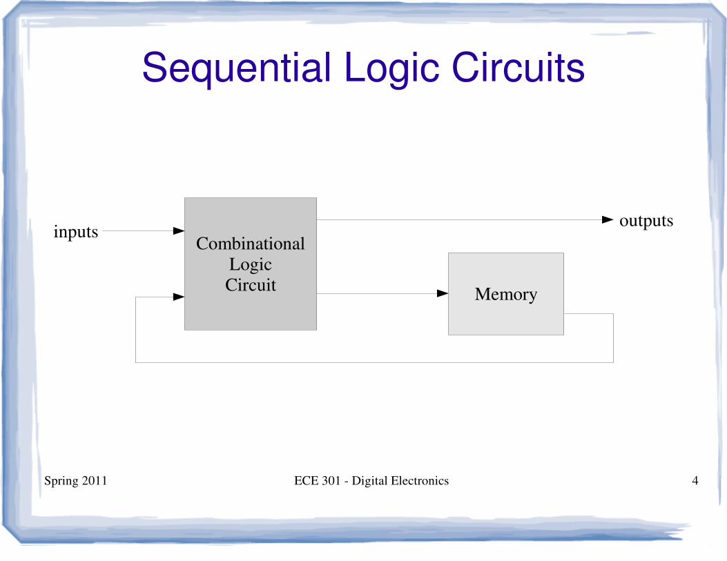
Sequential Logic Circuits
● The output of a sequential logic circuit is dependent not only on the present inputs, but also on the past sequence of the inputs.
● A sequential logic circuit must “remember” the past history of the inputs.
● It does this using basic memory elements.
– Latches
– Flip-Flops
Spring 2011 ECE 301 - Digital Electronics 4
Sequential Logic Circuits
Combinational
Logic
CircuitMemory
inputsoutputs
Spring 2011 ECE 301 - Digital Electronics 5
Basic Memory Elements
Spring 2011 ECE 301 - Digital Electronics 6
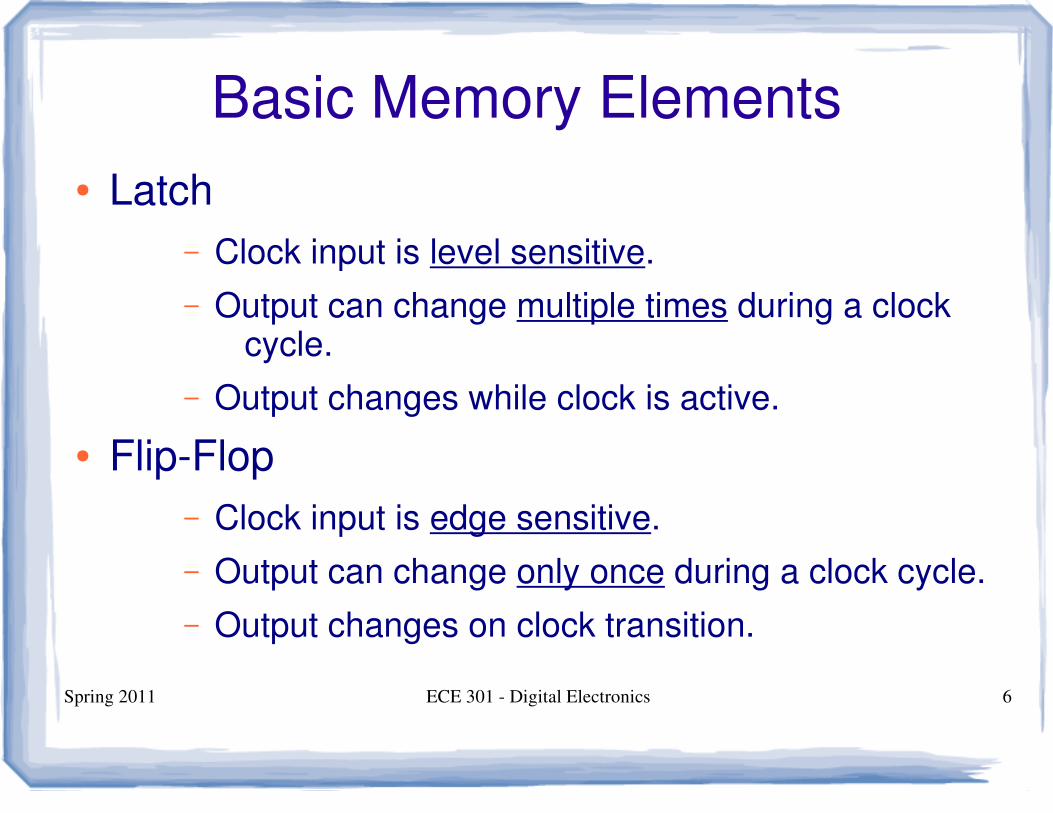
Basic Memory Elements
● Latch
– Clock input is level sensitive.
– Output can change multiple times during a clock cycle.
– Output changes while clock is active.
● Flip-Flop
– Clock input is edge sensitive.
– Output can change only once during a clock cycle.
– Output changes on clock transition.
Spring 2011 ECE 301 - Digital Electronics 7
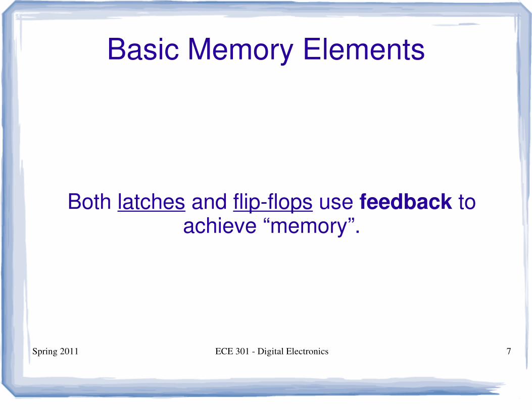
Basic Memory Elements
Both latches and flip-flops use feedback to achieve “memory”.
Spring 2011 ECE 301 - Digital Electronics 8
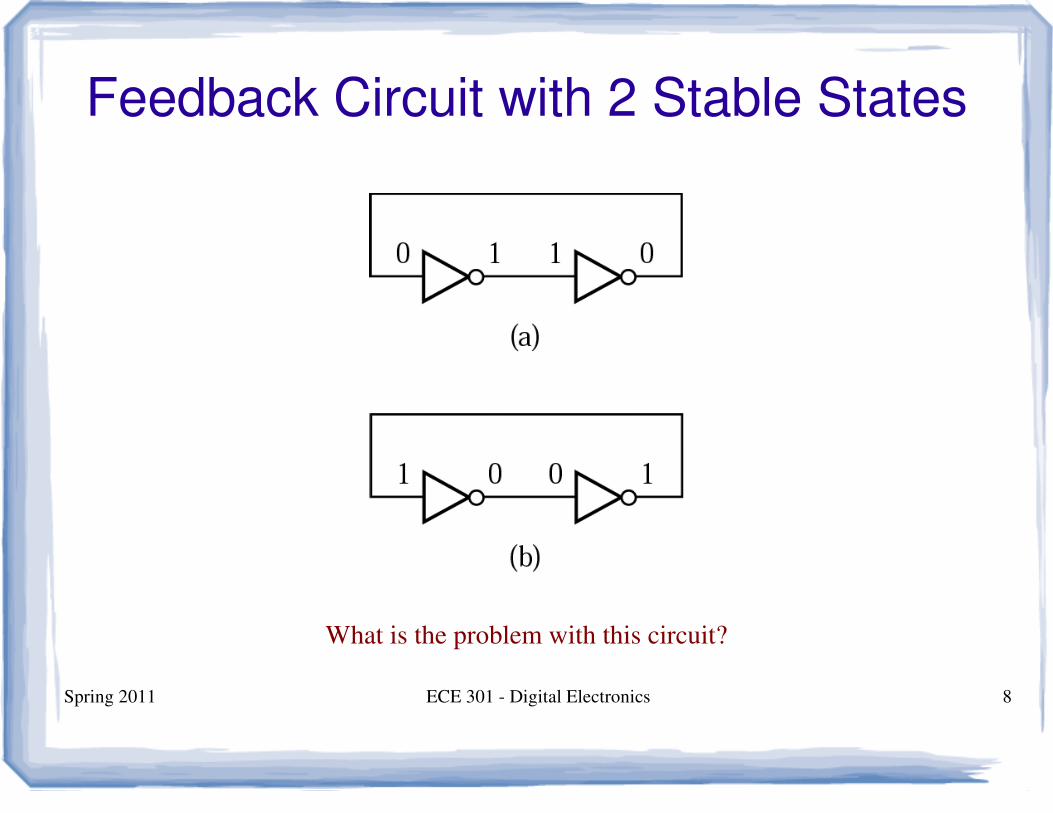
Feedback Circuit with 2 Stable States
What is the problem with this circuit?
Spring 2011 ECE 301 - Digital Electronics 9
Latches
Spring 2011 ECE 301 - Digital Electronics 10
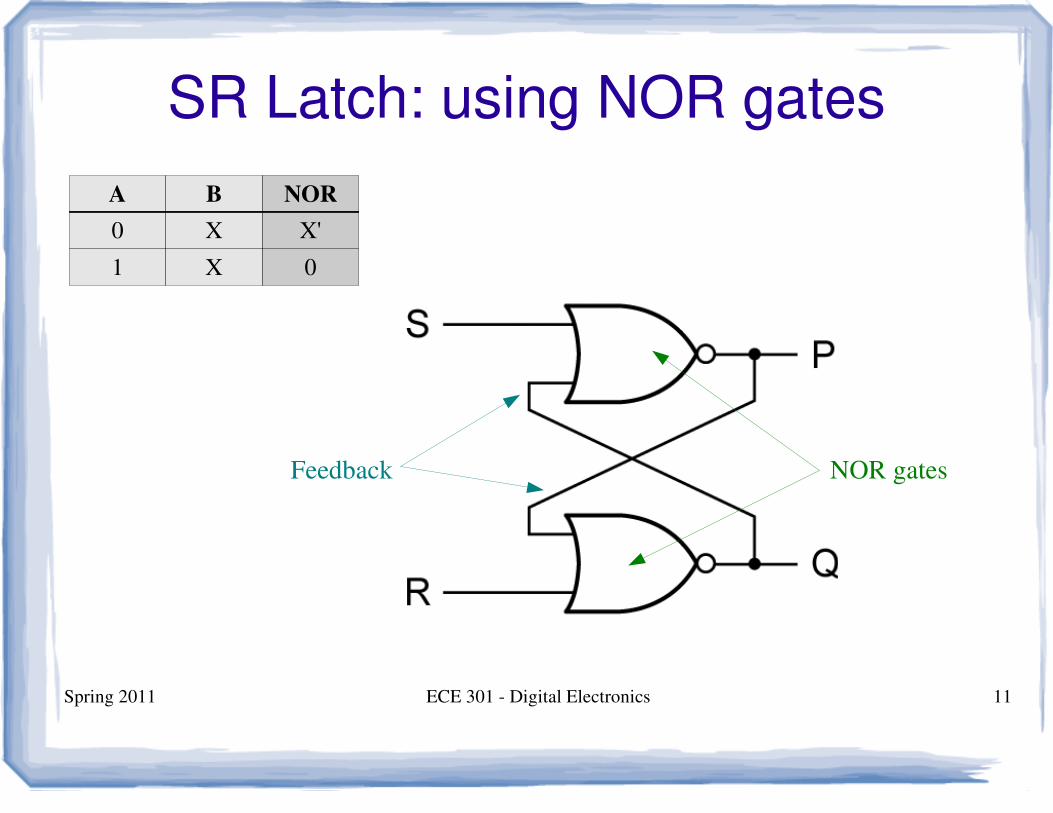
Set-Reset (SR) Latch
● A Set-Reset Latch has two inputs
– Set (S) input
– Reset (R) input
● It can be constructed from two cross-coupled NOR gates or two cross-coupled NAND gates.
● It has three modes of operation
– Set: Latch output set to 1 (Q+ = 1)
– Reset: Latch output reset to 0 (Q+ = 0)
– Store: Latch output does not change (Q+ = Q)
Spring 2011 ECE 301 - Digital Electronics 11
SR Latch: using NOR gates
A B NOR
0 X X'
1 X 0
Feedback NOR gates
Spring 2011 ECE 301 - Digital Electronics 12
SR Latch: Set (S = 1, R = 0)
A B NOR
0 X X'
1 X 0
1
01
0
P = Q'
Spring 2011 ECE 301 - Digital Electronics 13
SR Latch: Reset (S = 0, R = 1)
A B NOR
0 X X'
1 X 0
0
10
1
P = Q'
Spring 2011 ECE 301 - Digital Electronics 14
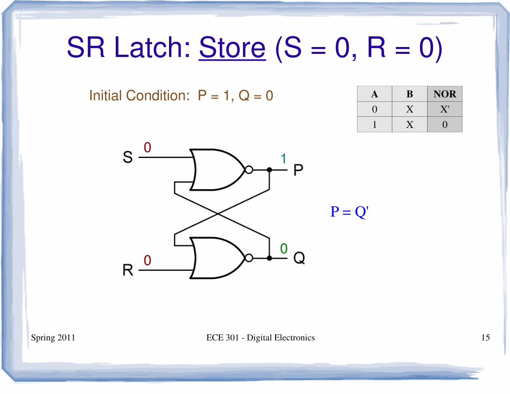
SR Latch: Store (S = 0, R = 0)
A B NOR
0 X X'
1 X 0
0
01
0
P = Q'
Initial Condition: P = 0, Q = 1
Spring 2011 ECE 301 - Digital Electronics 15
SR Latch: Store (S = 0, R = 0)
A B NOR
0 X X'
1 X 0
0
00
1
P = Q'
Initial Condition: P = 1, Q = 0
Spring 2011 ECE 301 - Digital Electronics 16
• If S = 1 (Set), Q+ = 1
• If R = 1 (Reset), Q+ = 0
• If S = R = 0, Q+ = Q (no change)
• S = R = 1 is not allowed.
SR Latch: Behavior
Nextvalue
Presentvalue
S R Q Q+
0 0 0 0
0 0 1 1
0 1 0 0
0 1 1 0
1 0 0 1
1 0 1 1
1 1 0 not
1 1 1 allowed
Spring 2011 ECE 301 - Digital Electronics 17
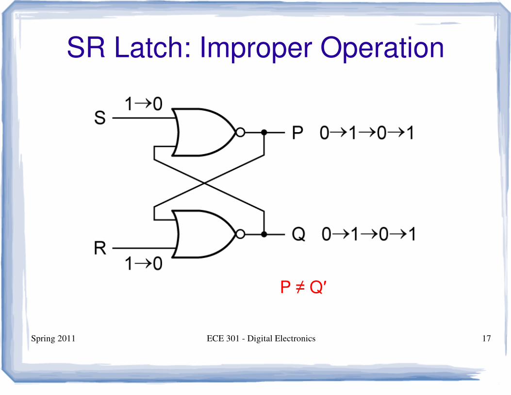
P ≠ Q′
SR Latch: Improper Operation
Spring 2011 ECE 301 - Digital Electronics 18
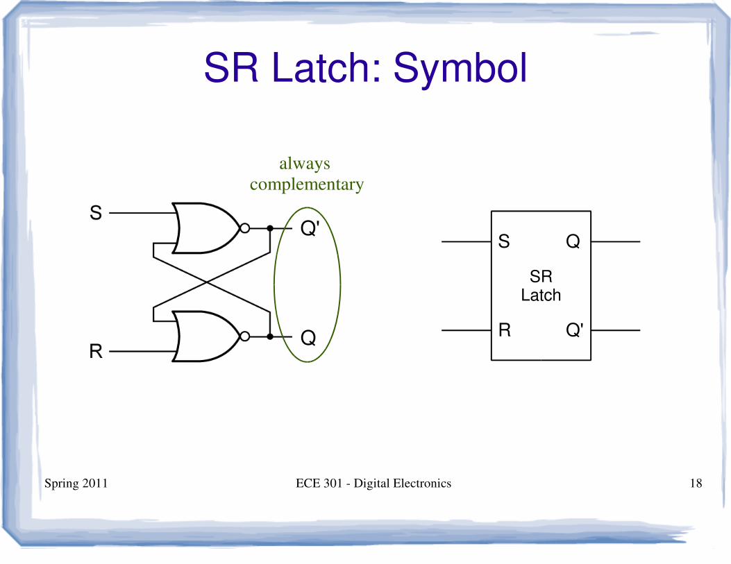
SR Latch: Symbol
Q'
Q
SRLatch
S
R
Q
Q'
always
complementary
Spring 2011 ECE 301 - Digital Electronics 19
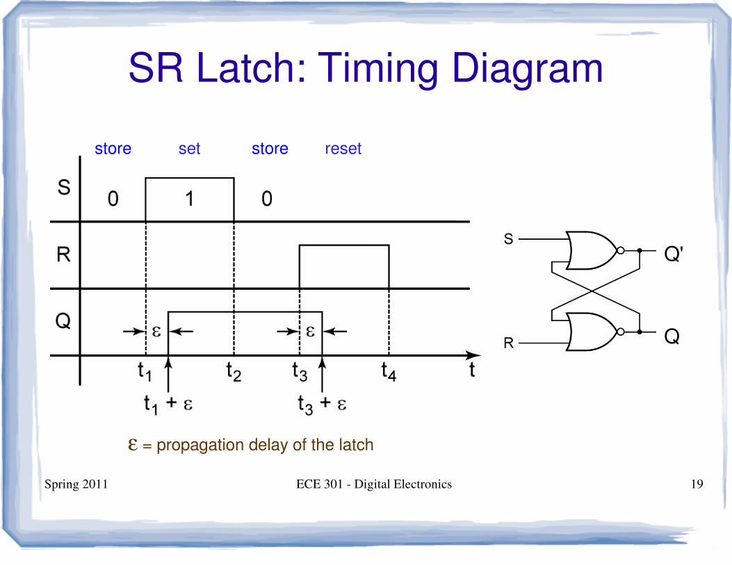
SR Latch: Timing Diagram
store set store reset
ε = propagation delay of the latch
Q'
Q
Spring 2011 ECE 301 - Digital Electronics 20
SR Latch: Characteristic Equation
Characteristic Equation: Q+ = S + R'.Q (S.R = 0)
Q = present state
Q+ = next state
Spring 2011 ECE 301 - Digital Electronics 21
SR Latch: using NAND gates
A B NAND
0 X 1
1 X X'
S' R' Q Q+
1 1 0 0
1 1 1 1
1 0 0 0
1 0 1 0
0 1 0 1
0 1 1 1
0 0 0 not
0 0 1 allowed
Spring 2011 ECE 301 - Digital Electronics 22
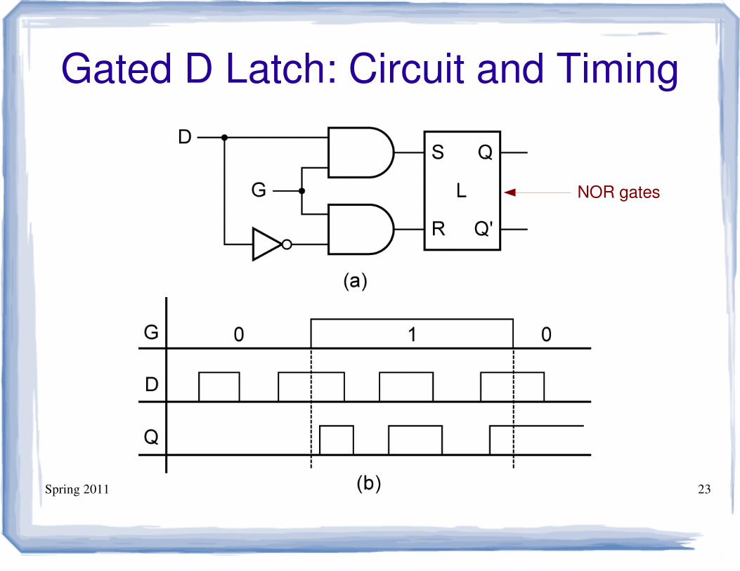
Gated D Latch
● A Gated D Latch has two inputs
– Gate (G) input
– Data (D) input
● It can be constructed from an SR Latch and additional logic gates.
● It has the following behavior
– G = 1: D is passed to Q (Q+ = D)
– G = 0: Q remains unchanged (Q+ = Q)
● Also referred to as a transparent latch.
Spring 2011 ECE 301 - Digital Electronics 23
Gated D Latch: Circuit and Timing
NOR gates
Spring 2011 ECE 301 - Digital Electronics 24
Gated D Latch: Symbol and Truth Table
No invalid inputs!
Spring 2011 ECE 301 - Digital Electronics 25
Gated D Latch: Characteristic Equation
Characteristic Equation: Q+ = G'.Q + G.D
0
1
2
3
6
7
4
5
Spring 2011 ECE 301 - Digital Electronics 26
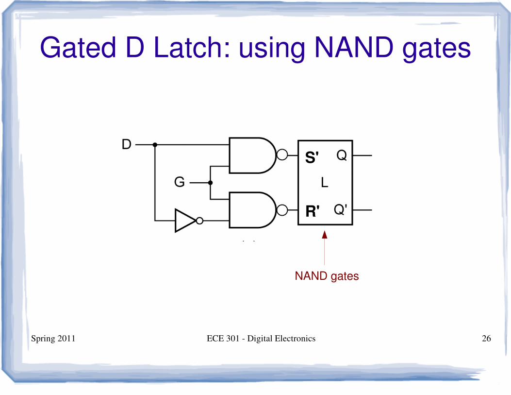
Gated D Latch: using NAND gates
S'
R'
NAND gates
Spring 2011 ECE 301 - Digital Electronics 27
Flip-Flops
Spring 2011 ECE 301 - Digital Electronics 28
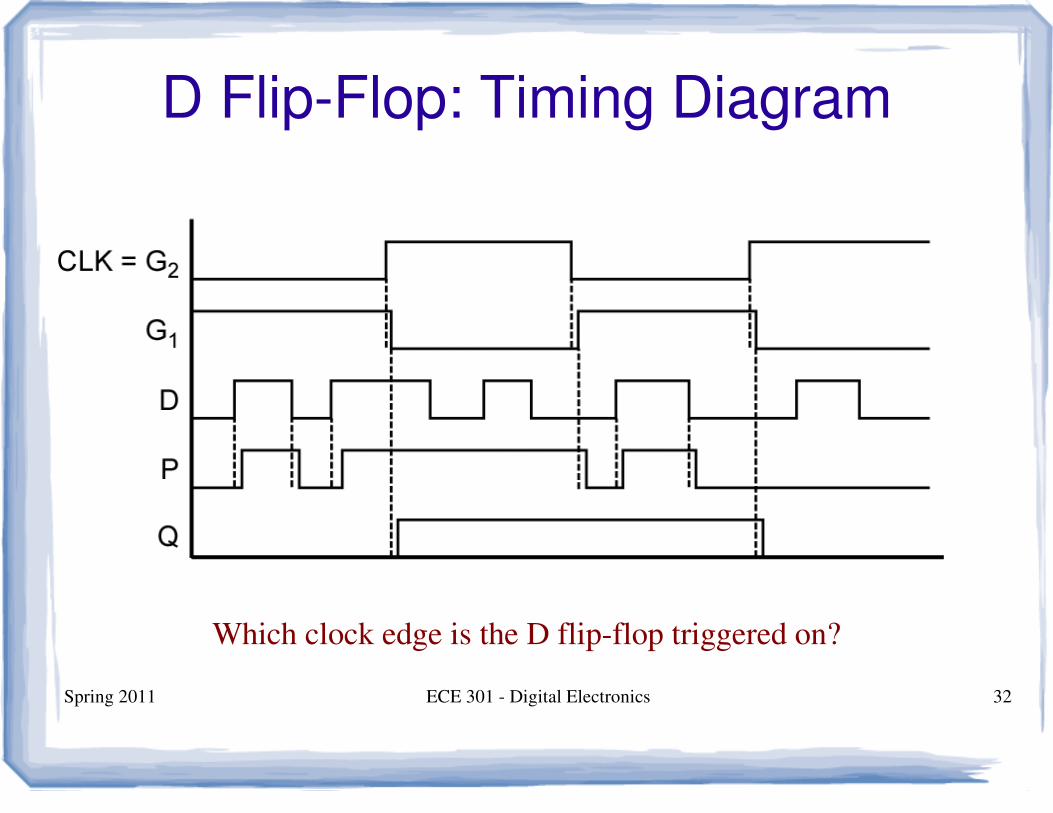
D Flip-Flop
● A D Flip-Flop has two inputs
– Clock (Ck) --- denoted by the small arrowhead
– Data (D)
● The output of the D Flip-Flop changes in response to the clock input only.
– not in response to a change in the D input
● The D Flip-Flop is edge-triggered not level-sensitive