Page 1
Page 1 of 25 Revised: 2/11/2020 10:22
ECE 3274 BJT amplifier design CE, CE with Ref, and CC.
Richard Cooper
Section 1: CE amp Re completely bypassed (open Loop)
Section 2: CE amp Re partially bypassed (gain controlled).
Section 3: CC amp (open loop)
Section 1: Common Emitter CE Amplifier Design
Vout is inverted so the gain Av and Ai are negative.
Designing procedure of common emitter BJT amplifier has three areas. First, we have to
set the Q-point, which is the DC operating point. Since, no specification regarding the Q-point
is mentioned in the design requirements; it leaves the designer enough freedom to choose
the operating point as necessary for the application. However, remember that the
specifications given in terms of input and output impedance, gain, frequency response
characteristics and peak output voltages ultimately restricts the Q-point in a narrow window. It
is difficult derive the Q-point without some intelligent guess and the following steps would
work out for the given conditions. We will start to choose a Q-point to allow maximum output
voltage swing.
In this configuration, RE is completely bypassed. The circuit diagram with necessary variables
is provided in CE Figure 1.
Page 2
Page 2 of 25 Revised: 2/11/2020 10:22
Ri
Rb1
Rc
Rload
Rgen
50
Function
Generator
Cin
Cout
Cbyp
Ce
2N2222
Chi
Vcc
Vcc
Re
Rin2
Vin
Vout
Rout
Rin
Chi2
Vin2
Vb
Ve
CE Figure 1: BJT Common Emitter
Page 3
Page 3 of 25 Revised: 2/11/2020 10:22
BJT Figure 2: BJT characteristics. The example not your Q-point
Step CE 1.1: Measure the device parameters
For the design of the amplifier, the 3 parameter values required are ro and gm. Derived from the
transistor characteristics curve shown in CE Figure 2, one can set an approximate Q-point (VCE
and IC) in the active region and measure ro and β. We will solve for Vce and estimate IC.
Solve for VCE see below Step CE2.2 . Use Vout peak to find Iload peak: Iload = Vout / Rload.
Page 4
Page 4 of 25 Revised: 2/11/2020 10:22
For an approximate IC Q-point use IC ≈ 2.2 * Iload peak this is not the solution to your design Q-
point. We can use an approximate IC because ro and β will not very much with small changes in
Q-point.
The VceSAT (Vce saturation voltage) is found from the BJT characteristics curve where the curve
begins to flatten out ≈ 0.2 Vdc.
ro = ΔVCE / ΔIC the slope of a line thru Q-point
βAC = ΔIC / ΔIB measured around Q-point
VceSAT = Vce begins to flatten
rπ = ( β VT ) / IC rπ is base to emitter resistance Hybrid Pie model.
Where VT = kT/q at room temperature is VT ≈ 26mV.
Plot the estimated Q-point (VCE,IC) on the BJT characteristics curve.
Plot the estimated Q-point (VCE,IC) on the BJT characteristics curve.
CE Part 2: Determine the Q-point.
Start with your BJT and selecting 4 resistors.
Step CE2.1: Choose VE
Because VBE will decrease ≈ 2.5mV / ˚ C rise we set VE = between 2V to 3V. VE and RE will
provide negative feedback to stabilize β and VBE.
Step CE2.2: Calculate the midpoint VC with Re complete bypassed Re = Reb, and Ref = 0
Midpoint selection will allow for maximum output voltage swing.
We will add 20% to Vout so the design is not on the edge of the solution.
VC(max) = VCC - (Vout + 20%Vout)
VC(min) = VE+VCE sat + (Vout + 20%Vout)
VC = (VC(max) + VC(min)) / 2 Midpoint VC Q-point
VCE = VC – VE This is the Q-point VCE
Step CE2.3: Calculate RC .
The DC equation: VCC – VC = VRC= RC IC voltage across Rc derived from Vcc and Q-point Vc.
The AC equation: Vout = ic ( RC || ro || RL ) output voltage Voutpeak
Rewrite: Vout = ic Rc (ro || RL) / (Rc + (ro || RL)) Parallel resistance equation
Substituting in vRC = ic RC
Combined equation: Vout = VRC (ro || RL) / (Rc + (ro || RL))
Solve for Rc; Add 20%Vout so the collector current is not set to an edge.
RC = VCC− VC
Vout+20%𝑉𝑜𝑢𝑡 (ro ∥ RL ) − (ro ∥ RL )
Step CE2.4: Calculate IC, IE, and Re.
Page 5
Page 5 of 25 Revised: 2/11/2020 10:22
IC = (VCC – VC) / RC The Q-point collector current.
IB = IC / β The base current.
IE = IC (β + 1) / β emitter current.
Re = VE / IE Total emitter resistance.
Thus, Q-point is (VCE, IC).
AC
Rloadro
Rb
Ri
Rgen
Vin
Vout
B
E
C
Rin
Rin2 Rout
Vin2NPN
β Ib
RcRπ
Ib
CE Figure 3: Common Emitter Small Signal Equivalent Circuit
CE Part 3: Determine bias resistors.
Step CE3.1: Calculate RE. Design for the sum Ref and Reb
Later we will design for a desired Av (voltage gain) by using (Ref) and (Reb) to control the Av.
RE = Ref + Reb
IE = IC (β +1) / β
IB = IC / β
∴ RE =VE
IE
Step CE3.2: Calculate Rb1, Rb2. Method 1.
(Do not use Method 1 for your design.) Use step CE 3.3
VB = VE + VBE VBE is normally between 0.6V and 0.7V
Page 6
Page 6 of 25 Revised: 2/11/2020 10:22
Ib = Ic / β
Current thru Rb1 is set to 10 * IB
Current thru Rb2 is set to 9 * IB
Rb1 = (Vcc – VB )/ (10* IB )
Rb2 = VB / (9 * IB)
Step CE3.3: Calculate Rb1, Rb2. Method 2.
(Use this Method)
Require Rin set to a given value. Need Vcc, Vb, rπ and Ib.
Given Rin calculate Rin2.
Rin2 = Rin –Ri Solve Rin2 needed to Rin requirements.
Solve for Rb from Rin2 and Rbase.
Rbase = rπ Re completely bypassed.
Rb = 1 /((1 / Rin2 ) – (1 / Rbase )) Solve for Rb needed to Rin requirements.
Find Rb1 first then Rb2
Rb1 = Vcc / (( Vb / Rb ) + Ib) Solve for Rb1.
Rb2 = Vb / ((( Vcc –Vb) /Rb1) –Ib ) Solve Rb2 from Vb and current thru Rb2: Irb2 = Irb1 – Ib
Check Rin meets requirements
Rbase = rπ Re completely bypassed.
Rb = Rb1 || Rb2.
Rin2 = Rb || Rbase
Rin = Ri + Rin2
CE Part 4: Calculating impedance and Gain
Vout is inverted so the Voltage gain Av is negative.
Page 7
Page 7 of 25 Revised: 2/11/2020 10:22
Refer to the small signal equivalent of the circuit you have just built in CE Fig. 3. We can
calculate the following:
Step CE4.1: Input Impedance: AC characteristics
Rb = Rb1 || Rb2 the two base bias resistors.
If Re completely bypassed with CE then
Rbase = rπ
Rin2 = Rb || Rbase
Rin = Ri + Rin2
Step CE4.2: Output Impedance
If Re completely bypassed with CE then
Rout = RC || r0. With Ref = 0
Step CE4.3: Voltage Gain
AC voltage Vout = - β Ib (Rout || Rload || ro) Note: use the correct Rout depending on Ref
AC voltage Vin = (Rin/Rin2) Vin2 Input signal from the function generator.
AC voltage Vin2 = vb Input signal on the base
Av2 = Vout / Vin2 = -β (Rc || ro || Rload) / rπ voltage gain at base. Av2 is negative.
Av = Vout / Vin = - β (Rc || ro || Rload) / ((Rin2+Ri) / Rin2) ( rπ ) Av is negative.
Rearrange Av = - β (Rin2 / (Rin2 + Ri)) * (Rd || ro || Rload) / rπ
Vgen = ((Rin + Rgen) / Rin ) * (Vout/ Av) the open circuit voltage of the function generator.
Step CE4.4: Current Gain
Ai =𝐼𝑙𝑜𝑎𝑑
𝐼𝑖𝑛=
𝑉𝑜𝑢𝑡𝑅𝑙𝑜𝑎𝑑⁄
𝑉𝑖𝑛𝑅𝑖𝑛⁄
= AvRin
Rload
Step CE4.5: Power gain
G = Pout / Pin = Vout * Iload / Vin * Iin = Av * Ai
In decibels GdB = 10log ( Av * Ai )
Step CE4.6: Vin and Voc of Vgen
Input signal level need to produce the required output voltage.
Vin = Vout / Av
Page 8
Page 8 of 25 Revised: 2/11/2020 10:22
The open circuit voltage of the generator to produce the required output voltage.
Because of Voltage divider because the output impedance of the Rgen = 50Ω
Vgen = Vin (Rgen + Rin) / Rin
Use this value in LTspice and the laboratory Function generator
CE Part 5: Frequency response
With the Q-point being set after the sequence of steps, we can go for the selection of capacitors
and finally connect the signal generator at input and measure the output amplified waveform.
First we will select Cin, Cout and CE which jointly would set the roll-off beyond the lower cut-off
frequency. Set any frequency within the range as your lower cut-off frequency and let us call it
fL. Three capacitors will introduce 3 zeros in the transfer function of the system. Because we will
set 3 zeros at the same frequency we must use the Band Width Shrinkage factor.
BWshrinkage = √21
𝑛 − 1
Where n is the number of zeros for low frequency breakpoints at same frequency.
Setting 3 frequencies equal, we get,
fCin = fCout = fCE = fL √2
13⁄ − 1
Find the C for each breakpoint fCin , fCout , and fCE where n = 3.
C = 1
2πfC (R seen by C)
Where C is the capacitor that sets the breakpoint fC
RemitterBase is the impedance looking in the BJT emitter to base.
RemitterbBase = (rπ + Rb || (Ri + Rgen)) / (β + 1) Small value
R is the Thevenin equivalent resistance seen by the capacitor.
RCE = Re || (ro + RC || RLoad) || RemitterBase)
Page 9
Page 9 of 25 Revised: 2/11/2020 10:22
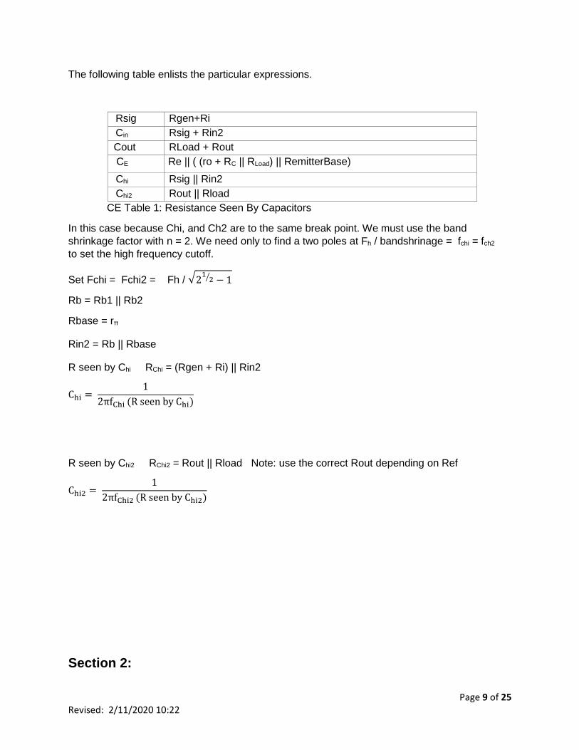
The following table enlists the particular expressions.
Rsig Rgen+Ri
Cin Rsig + Rin2
Cout RLoad + Rout
CE Re || ( (ro + RC || RLoad) || RemitterBase)
Chi Rsig || Rin2
Chi2 Rout || Rload
CE Table 1: Resistance Seen By Capacitors
In this case because Chi, and Ch2 are to the same break point. We must use the band
shrinkage factor with n = 2. We need only to find a two poles at Fh / bandshrinage = fchi = fch2
to set the high frequency cutoff.
Set Fchi = Fchi2 = Fh / √21
2⁄ − 1
Rb = Rb1 || Rb2
Rbase = rπ
Rin2 = Rb || Rbase
R seen by Chi RChi = (Rgen + Ri) || Rin2
Chi = 1
2πfChi (R seen by Chi)
R seen by Chi2 RChi2 = Rout || Rload Note: use the correct Rout depending on Ref
Chi2 = 1
2πfChi2 (R seen by Chi2)
Section 2:
Page 10
Page 10 of 25 Revised: 2/11/2020 10:22
CEwRef Common Emitter with Re that partially is bypassed by Ce.
Vout is inverted so the gain Av and Ai are negative.
RE = Ref + Reb the total RE for the DC bias design.
Ref is the portion of Re that is not bypassed by Ce.
Reb is the portion of Re that is bypassed by Ce.
CEwRef Part 1: Measure the device parameters
For the design of the amplifier, the 3 parameter values required are VceSAT, ro and β. Derived
from the transistor characteristics curve shown in BJT Figure 2 above, one can set an
approximate Q-point (VCE and IC) in the active region and measure ro and β. We will solve for
Vce and estimate IC.
Solve for VCE see below Step CEwRef 2.2. Use Vout peak to find Iload peak: Iload = Vout /
Rload.
For an approximate IC Q-point use IC ≈ 2.2 * Iload peak this is not the solution to your design Q-
point. We can use an approximate IC because ro and β will not very much with small changes in
Q-point.
The VceSAT (Vce saturation voltage) is found from the BJT characteristics curve where the curve
begins to flatten out ≈ 0.2 Vdc.
ro = ΔVCE / ΔIC the slope of a line thru Q-point
βAC = ΔIC / ΔIB measured around Q-point
VceSAT = Vce begins to flatten
rπ = ( β VT ) / IC rπ is base to emitter resistance Hybrid Pie model.
Where VT = kT/q at room temperature is VT ≈ 26mV.
Plot the estimated Q-point (VCE,IC) on the BJT characteristics curve.
CEwRef Part 2: Determine the Q-point.
Start with your BJT and selecting 4 resistors.
Step CEwRef 2.1: Choose VE
Because VBE will decrease ≈ 2.5mV / ˚ C rise we set VE = between 2V to 3V. VE and RE will
provide negative feedback to stabilize β and VBE.
Step CEwRef 2.2: Calculate the midpoint VC with Re partially bypassed Re = Reb + Ref
Page 11
Page 11 of 25 Revised: 2/11/2020 10:22
Midpoint selection will allow for maximum output voltage swing.
We will add 20% to Vout so the design is not on the edge of the solution. This will also help
with the additional loading because of high frequency capacitors as the frequency
approaches the high frequency break points.
VC(max) = VCC - (Vout + 20%Vout)
VC(min) = VE+VCE sat + (Vout + 20%Vout)
VC = (VC(max) + VC(min)) / 2 Midpoint VC Q-point
VCE = VC – VE This is the Q-point VCE
Step CEwRef 2.3: Calculate RC .
Looking into the collector we see ro + Ref || [ (rπ + Rb1|| Rb2 || (Ri +Rgen) ] / (β +1) ≈ ro so we
will use just ro .
The DC equation: VCC – VC = VRC= RC IC voltage across Rc derived from Vcc and Q-point Vc.
The AC equation: Vout = ic ( RC || ro || RL ) output voltage Voutpeak
Rewrite AC: Vout = ic Rc (ro || RL) / (Rc + (ro || RL)) Parallel resistance equation
Substituting in vRC = ic RC
Combined equation: Vout = VRC (ro || RL) / (Rc + (ro || RL))
Solve for Rc; Add 20%Vout so the collector current is not set to an edge.
RC = VCC− VC
Vout+20%𝑉𝑜𝑢𝑡 (ro ∥ RL ) − (ro ∥ RL )
Step CEwRef 2.4: Calculate IC, IE, and Re.
IC = (VCC – VC) / RC The Q-point collector current.
IB = IC / β The base current.
IE = IC (β + 1) / β emitter current.
Re = VE / IE Total emitter resistance.
Thus, Q-point is (VCE, IC).
We have already choose VE to be between 2V to 3V to provide negative feedback in the DC
bias circuit. We will use Ve and IC where Ie = ((β +1) / β) Ic. Now calculate Re =Ie (Ref +Reb)
the total emitter resistance.
We now have, Ve, Vc, Rc, Re, Ic, Ie, Vce, VceSAT
Page 12
Page 12 of 25 Revised: 2/11/2020 10:22
Ri
Rb1
Rb2
Rc
Rload
Rgen
50
Function
Generator
Cin
Cout
Cbyp
Ce
2N2222
Chi
Vcc
Vcc
Ref
Reb
Rin2
Vin
Vout
Rout
Rin
Chi2
Vin2
Vb
Ve
CEwRef Figure 1: Amplifier with emitter partially bypassed.
AC
Rloadro
Rb
Ri
Rgen
Vin
Vout
B
E
C
Rin
Rin2 Rout
Vin2NPN
β Ib
RcRπ
Ib
Ref Ie
CEwRef Figure 2: Small signal model with partial bypass of Re
Page 13
Page 13 of 25 Revised: 2/11/2020 10:22
CEwRef Part 3 Calculating impedance and Gain with Ref
Remember the gain Av and Ai are negative for a common emitter amplifier.
We use the same Q-point and bias resistors Rb1, Rb2, Rc, and Re = Ref + Reb.
Step CEwRef3.1: find Ref based on Voltage Gain requested
Note: ib is the AC base current that results from Vin.
Looking into the collector we see ro + Ref || [ (rπ + Rb1|| Rb2 || (Ri +Rgen) ] / (β +1) ≈ ro so
we will use just ro .
AC voltage Vout = - β ib (Rc || Rload || ro) Note: use the approximant ro because Ref is not
known yet.
AC voltage Vin = (Rin/Rin2) Vin2 Input signal from the function generator.
AC voltage Vin2 = ib(rπ + (β + 1) Ref) Input signal on the base
Given Rin calculate Rin2.
Rin2 = Rin –Ri Solve Rin2 needed to meet the Rin requirements.
Av2 = Av * Rin / Rin2 Av2 at base needed to meet Av requested. For CE Av is negative.
Av2 = Vout / Vin2 = -β (Rc || ro || Rload) / (rπ + (β + 1) Ref) voltage gain at base, we do not
need to find ib since ib cancels. Av2 is negative which means that Vout is inverted.
Step CEwRef3.2: Solve for Ref by using gain at base Av2.
Ref = = [ ( -β (Rc || ro || Rload) / Av2 ) - rπ ] / ( β + 1) from Av2 or use equation below
Step CEwRef3.3: Solve for Ref by using overall gain Av.
Av = Av2 * Rin2 / Rin
Av = Vout / Vin = - β (Rc || ro || Rload) / (Rin/Rin2) (rπ + (β + 1) Ref) voltage gain at input
We can see that voltage gain Av can be controlled by the value of Ref
Av = - β (Rin2/Rin) (Rc || ro || Rload) / (rπ + (β + 1) Ref)
Rearrange Av to solve for Ref from requested Av
Ref = -( (β (Rin2/Rin) (Rc|| ro || Rload) / Av) - rπ) / (β + 1) from Av overall gain, Av is negative
Step CEwRef3.4: Solve for Reb from Re and Ref
Remember that Re is the total emitter residence from step CEwRef 2.4.
Reb = Re – Ref
Page 14
Page 14 of 25 Revised: 2/11/2020 10:22
Step CEwRef4.1: Rb1 and Rb2 based on requested Rin
Require Rin set to a given value. Need Vcc, Vb, rπ and IB (DC bias base current).
Given Rin calculate Rin2.
Rin2 = Rin –Ri Solve Rin2 needed to meet the Rin requirements.
Solve for Rb from Rin2 and Rbase.
Rbase = rπ + (β + 1) (Ref || (ro + Rc || Rload)) Looking into the Base of the BJT.
Rb = 1 /((1 / Rin2 ) – (1 / Rbase )) Solve for Rb needed to Rin requirements.
Find Rb1 first then Rb2
IB = IC / β DC bias base current.
Rb1 = Vcc / (( Vb / Rb ) + Ib) Solve for Rb1.
Rb2 = Vb / ((( Vcc –Vb) /Rb1) –Ib ) Solve Rb2 from Vb and current thru Rb2: Irb2 = Irb1 – Ib
Check Rin meets requirements
Rbase = rπ + (β + 1) (Ref || (ro + Rc || Rload)
Rb = Rb1 || Rb2.
Rin2 = Rb || Rbase
Rin = Ri + Rin2
Step CEwRef4.2: Input Impedance: AC characteristics
Rb = Rb1 || Rb2
Where Ref is the part of RE that is not bypassed by CE.
Rbase = rπ + (β + 1) (Ref || (ro + Rc || Rload)) Looking into the Base of the BJT.
Rin2 = Rb || Rbase
Rin = Ri + Rin2
Page 15
Page 15 of 25 Revised: 2/11/2020 10:22
Step CEwRef4.3: Output Impedance with Ref
If Re partially bypassed with CE bypassing Ref.
Rb = Rb1 || Rb2.
RemitterBase is the impedance looking in the BJT emitter toward the base.
RemitterBase = (rπ + Rb || (Ri + Rgen)) / (β + 1) Small value, because divided by β +1.
The complete equation below for Rout,
Rout = RC || ( r0 + Ref || [rπ + Rb || (Ri + Rgen) ] / (β +1))
Because ro is greater than 30kΩ we approximate Rout = Rc || “large” = Rc
Step CEwRef4.4: Current Gain
The current gain Ai can be obtained iload and iin or calculated from Av Rin and Rload.
Ai =𝐼𝑙𝑜𝑎𝑑
𝐼𝑖𝑛=
𝑉𝑜𝑢𝑡𝑅𝑙𝑜𝑎𝑑⁄
𝑉𝑖𝑛𝑅𝑖𝑛⁄
= AvRin
Rload
Step CEwRef4.5: Power gain
G = Pout / Pin = Vout * Iload / Vin * Iin = Av * Ai
In decibels GdB = 10log ( Av * Ai )
Step CEwRef4.6: Vin and Voc of Vgen
Input signal level need to produce the required output voltage.
Vin = Vout / Av
The open circuit voltage of the generator to produce the required output voltage.
Because of Voltage divider because the output impedance of the Rgen = 50Ω
Vgen = Vin (Rgen + Rin) / Rin
Use this value in LTspice and the laboratory Function generator.
Page 16
Page 16 of 25 Revised: 2/11/2020 10:22
CEwRef Part 5: Frequency response with Ref
With the Q-point being set after the sequence of steps, we can go for the selection of capacitors
and finally connect the signal generator at input and measure the output waveform.
Step CEwRef 5.1: Low frequency cut off. FL
First we will select Cin, Cout and CE which jointly would set the roll-off beyond the lower cut-off
frequency. Set any frequency within the range as your lower cut-off frequency and let us call it
fL. Three capacitors will introduce 3 zeros in the transfer function of the system. Because we will
set 3 zeros at the same frequency we must use the Band Width Shrinkage factor.
BWshrinkage = √21
𝑛 − 1
Where n is the number of zeros for low frequency breakpoints at same frequency.
The low frequency cutoff average of the individual time constants with shrinkage faction apllided
be we have set all the time constants the same.
Setting 3 frequencies equal, we get,
fCin = fCout = fCE = fL √2
13⁄ − 1
Find the C for each breakpoint fCin , fCout , and fCE where n = 3.
C = 1
2πfC (R seen by C)
Where C is the capacitor that sets the breakpoint fC
R is the Thevenin equivalent resistance seen by the capacitor.
RemitterBase is the impedance looking in the BJT emitter to base.
RemitterbBase = (rπ + Rb || (Ri + Rgen)) / (β + 1) Small value
RCE = Reb || (Ref + (ro + RC || RLoad) || RemitterBase)
Page 17
Page 17 of 25 Revised: 2/11/2020 10:22
Step CEwRef 5.2: High frequency cut off. FH
Chi Sets the higher cut-off frequency fH which is to be set from the specified range.
In this case because Chi, and Ch2 are to the same break point. We must use the band
shrinkage factor with n = 2. We need only to find a two poles at Fh / bandshrinage = fchi = fch2
to set the high frequency cutoff.
Set Fchi = Fchi2 = Fh / √21
2⁄ − 1
Rb = Rb1 || Rb2 Base bias resistors
Rbase = rπ + (β + 1) (Ref || (ro + Rc || Rload)) Looking into the Base of the BJT.
Rin2 = Rb || Rbase
R seen by Chi RChi = (Rgen + Ri) || Rin2
Chi = 1
2πfChi (R seen by Chi)
R seen by Chi2 RChi2 = Rout || Rload Note: use the correct Rout depending on Ref
Chi2 = 1
2πfChi2 (R seen by Chi2)
The following table list the equivalent resistance expressions seen by the capacitors.
Rsig Rgen+Ri
RemitterBase (rπ + Rb || (Ri + Rgen)) / (β + 1)
Cin Rsig + Rin2
Cout RLoad + Rout
CE Reb || (Ref + (ro + RC || RLoad) || RemitterBase)
Chi Rsig || Rin2
Chi2 Rout || Rload
CEwRef Table 1: Resistance Seen By Capacitors
Page 18
Page 18 of 25 Revised: 2/11/2020 10:22
Section 3: Common Collector CC Amplifier Design
Vout is not inverted so the gain Av and Ai are positive.
Designing procedure of common collector BJT amplifier has three areas. First, we have to
set the Q-point, which is the DC operating point. Since, there is no specification regarding the
Q-point in the design requirements; it leaves the designer enough freedom to choose the
operating point as necessary for the application. However, remember that the specifications
are in terms of input and output impedance, gain, frequency response characteristics and
peak output voltages ultimately restricts the Q-point in a narrow window. It is difficult to derive
this point without some intelligent guess and the following steps would work out for the given
conditions. We will start to choose a Q-point to allow maximum output voltage swing
For the Common Collector configuration, the circuit diagram shown in CC Figure 1. The
small signal equivalent model in CC Figure 3.
For this configuration, same steps are involved for the calculation of Rb1, Rb2 and RE with few
minor changes. Note that RC is absent in this case
Ri
Rb1
Rb2
Rload
Rgen
50
Function
Generator
Cin
Cout
Cbyp
2N2222
Vcc Vcc
Re
Rin
Vin
Vout
Rout
Chi
Chi2
Vin2
Rin2
Vb
Riso
Figure 1: BJT Common Collector CC configuration
Page 19
Page 19 of 25 Revised: 2/11/2020 10:22
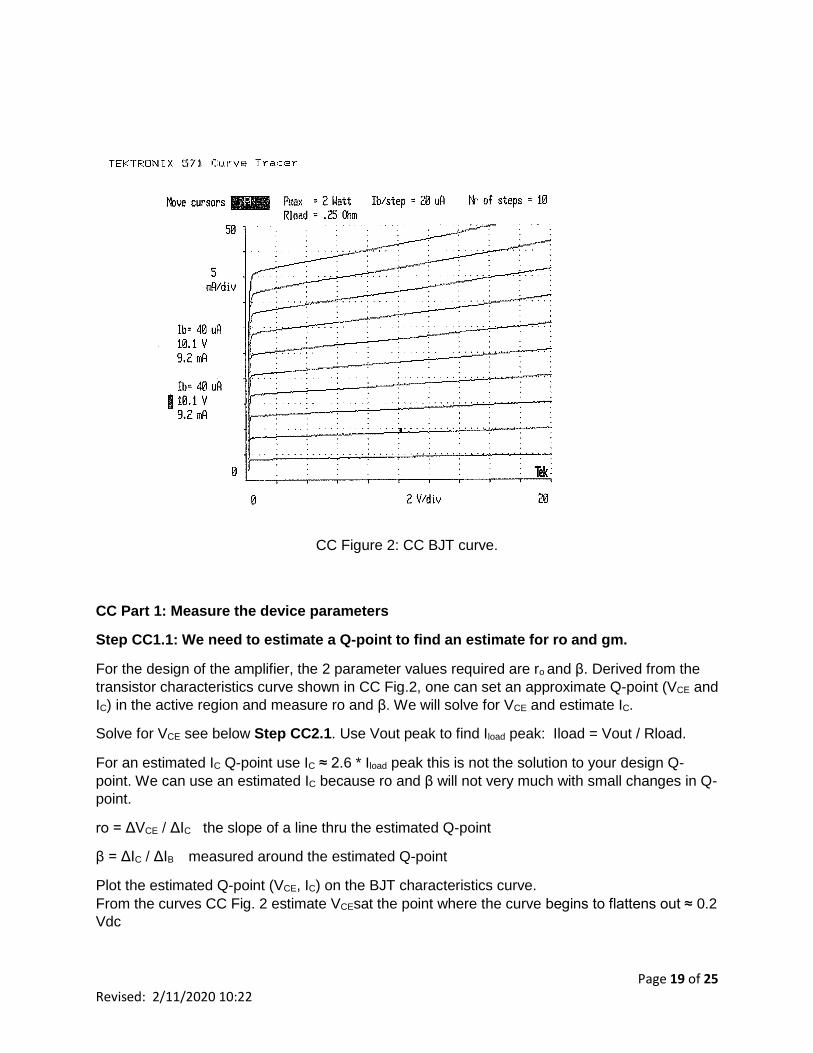
CC Figure 2: CC BJT curve.
CC Part 1: Measure the device parameters
Step CC1.1: We need to estimate a Q-point to find an estimate for ro and gm.
For the design of the amplifier, the 2 parameter values required are ro and β. Derived from the
transistor characteristics curve shown in CC Fig.2, one can set an approximate Q-point (VCE and
IC) in the active region and measure ro and β. We will solve for VCE and estimate IC.
Solve for VCE see below Step CC2.1. Use Vout peak to find Iload peak: Iload = Vout / Rload.
For an estimated IC Q-point use IC ≈ 2.6 * Iload peak this is not the solution to your design Q-
point. We can use an estimated IC because ro and β will not very much with small changes in Q-
point.
ro = ΔVCE / ΔIC the slope of a line thru the estimated Q-point
β = ΔIC / ΔIB measured around the estimated Q-point
Plot the estimated Q-point (VCE, IC) on the BJT characteristics curve.
From the curves CC Fig. 2 estimate VCEsat the point where the curve begins to flattens out ≈ 0.2
Vdc
Page 20
Page 20 of 25 Revised: 2/11/2020 10:22
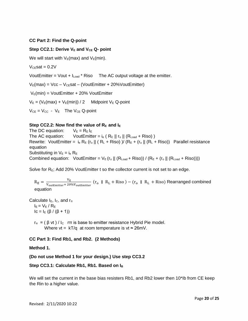
CC Part 2: Find the Q-point
Step CC2.1: Derive VE and VCE Q- point
We will start with VE(max) and VE(min).
VCEsat = 0.2V
VoutEmitter = Vout + ILoad * Riso The AC output voltage at the emitter.
VE(max) = Vcc – VCEsat – (VoutEmitter + 20%VoutEmitter)
VE(min) = VoutEmitter + 20% VoutEmitter
VE = (VE(max) + VE(min)) / 2 Midpoint VE Q-point
VCE = VCC - VE The VCE Q-point
Step CC2.2: Now find the value of RE and IE
The DC equation: VE = RE IE
The AC equation: VoutEmitter = ie ( RE || ro || (RLoad + Riso) )
Rewrite: VoutEmitter = ie RE (ro || ( RL + Riso) )/ (RE + (ro || (RL + Riso)) Parallel resistance
equation
Substituting in VE = ie RE
Combined equation: VoutEmitter = VE (ro || (RLoad + Riso)) / (RE + (ro || (RLoad + Riso))))
Solve for RE; Add 20% VoutEmitter t so the collector current is not set to an edge.
RE = VE
VoutEmitter+ 20%VoutEmitter (ro ∥ RL + Riso ) − (ro ∥ RL + Riso) Rearranged combined
equation
Calculate IE, IC, and rπ
IE = VE / RE
Ic = IE (β / (β + 1))
rπ = ( β vt ) / IC rπ is base to emitter resistance Hybrid Pie model.
Where vt = kT/q at room temperature is vt ≈ 26mV.
CC Part 3: Find Rb1, and Rb2. (2 Methods)
Method 1.
(Do not use Method 1 for your design.) Use step CC3.2
Step CC3.1: Calculate Rb1, Rb1. Based on IB
We will set the current in the base bias resisters Rb1, and Rb2 lower then 10*Ib from CE keep
the Rin to a higher value.
Page 21
Page 21 of 25 Revised: 2/11/2020 10:22
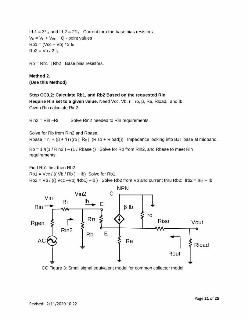
Irb1 = 3*IB and Irb2 = 2*IB Current thru the base bias resistors
VB = VE + VBE Q - point values
Rb1 = (Vcc – Vb) / 3 IB
Rb2 = Vb / 2 IB
Rb = Rb1 || Rb2 Base bias resistors.
Method 2.
(Use this Method)
Step CC3.2: Calculate Rb1, and Rb2 Based on the requested Rin
Require Rin set to a given value. Need Vcc, Vb, rπ, ro, β, Re, Rload, and Ib.
Given Rin calculate Rin2.
Rin2 = Rin –Ri Solve Rin2 needed to Rin requirements.
Solve for Rb from Rin2 and Rbase.
Rbase = rπ + (β + 1) ((ro || RE || (Riso + Rload))) Impedance looking into BJT base at midband.
Rb = 1 /((1 / Rin2 ) – (1 / Rbase )) Solve for Rb from Rin2, and Rbase to meet Rin
requirements.
Find Rb1 first then Rb2
Rb1 = Vcc / (( Vb / Rb ) + Ib) Solve for Rb1.
Rb2 = Vb / ((( Vcc –Vb) /Rb1) –Ib ) Solve Rb2 from Vb and current thru Rb2: Irb2 = Irb1 – Ib
ACRload
ro
Re
Rb
Ri
Rgen
Vin
Vout
E
E
C
Rin
Rin2
Rout
Vin2NPN
β Ib
Rπ
Ib
Riso
CC Figure 3: Small signal equivalent model for common collector model
Page 22
Page 22 of 25 Revised: 2/11/2020 10:22
CC Part 4: Calculate Rin, Rout, Av, and Ai
Step CC4.1: Input Impedance:
Rb = Rb1 || Rb2
Rbase = rπ + (β + 1) ((ro || RE ||(Riso + Rload))) Impedance looking into BJT base.
Rin2 = Rb || Rbase
Rin = Rin2 + Ri Note: Ri is the resistor in the input used as a shunt to measure input current.
Step CC4.2: Output Impedance
RemitterBase is the impedance looking in the BJT emitter towards the base.
RemitterBase = (rπ + Rb || (Ri + Rgen)) / (β + 1)
Rout = (RE || ro || RemitterBase) + Riso
Step CC4.3: Derivation of Av Voltage Gain
Av is positive: Vout is not inverted.
Referring to CC Fig.3, let us find Av = Vout / Vin which would be a key step in calculating Av.
Rbase = rπ + (β + 1) ((ro || RE || (Riso + Rload))) Impedance looking into BJT base.
Rb = Rb1 || Rb2
Rin2 = Rb || Rbase
Rin = Ri + Rin2
RemitterBase = (rπ + Rb || (Ri + Rgen)) / (β + 1) Impedance looking into the BJT emitter
towards the Base.
Rout = (RE || ro || RemitterBase) + Riso
AC Voltage at the emitter.
AC voltage VoutEmitter = ie (RE || ro || (Riso + Rload))
AC voltage VoutEmitter = (β + 1) ib (RE || ro || (Riso + Rload))
Voltage across the load resistor Vout = VoutEmitter * (Rload / (Rload +Riso))
AC voltage Vout = (β + 1) ib (RE || ro || (Riso + Rload)) * (Rload / (Rload +Riso))
Page 23
Page 23 of 25 Revised: 2/11/2020 10:22
AC Voltage at the function generator Vin = Vin2 (Rin / Rin2)
AC Voltage at the base Vin2 = VBE + VoutEmitter
Vin2 = Rπ ib + ib (β +1) (RE || ro || (Rload + Riso)) = ib (Rπ + (β+1) (Rs || ro || (Rload +Riso)))
Av2 = Vout / Vin2 = (β+ 1) ib (RE || ro || (Rload + Riso)) / ib (Rπ + (β+1) (RE || ro || (Rload +
Riso)))
Vin = Vin2 (Rin / Rin2) Voltage divider Vin to Vin2
Need Vout to find Av.
Vout = VoutEmitter * (Rload / (Rload +Riso)) Voltage divider VoutEmitter to Vout
Or rewriting VoutEmitter = Vout * ((Rload +Riso) / Rload) Find VoutEmitter from Vout.
Av = Vout / Vin = (Rin2 / Rin) (Rload /(Rload + Riso)) (β+ 1) ib (RE || ro || (Rload + Riso)) / ib (Rπ
+ (β+1) (RE || ro || (Rload + Riso)))
Canceling out ib and including the factor for Vin2 to Vin gives
This is the final equation for Av = Vout / Vin Av is positive: Vout is not inverted
Calculation of the Av.
Av = (Rin2 / Rin) (Rload /(Rload + Riso)) (β + 1) (RE || ro || (Rload + Riso)) / (Rπ + (β+1) (RE || ro
|| (Rload + Riso)))
Thus, the voltage gain should be close to 1. Hence, the output follows the input. So, the
Common Collector configuration is also known as an Emitter follower.
Step CC4.4: Calculation of the Ai Current Gain
Ai =𝐼𝑙𝑜𝑎𝑑
𝐼𝑖𝑛=
𝑉𝑜𝑢𝑡𝑅𝑙𝑜𝑎𝑑⁄
𝑉𝑖𝑛𝑅𝑖𝑛⁄
= AvRin
Rload
Page 24
Page 24 of 25 Revised: 2/11/2020 10:22
Step CC4.5: Power gain
G = Pout / Pin = Vout * Iload / Vin * Iin = Av * Ai
In decibels GdB = 10log ( Av * Ai )
Step CC4.6: Vin and Voc of Vgen
Input signal level need to produce the required output voltage.
Vin = Vout / Av
The open circuit voltage of the generator to produce the required output voltage.
Because of Voltage divider because the output impedance of the Rgen = 50Ω
Vgen = Vin (Rgen + Rin) / Rin
Use this value in LTspice and the laboratory Function generator.
CC Part 5: Frequency response.
The capacitor values can be calculated as before (CE amp), the only difference being n = 2 for
low pass calculations since we are using two capacitors instead of 3.
With the Q-point being set after the sequence of steps, we can go for the selection of capacitors
and finally connect the signal generator at input and measure the output amplified waveform.
Step CC5.1: Low frequency cut off. FL
First we will select Cin, and Cout which jointly would set the roll-off beyond the lower cut-off
frequency. Set any frequency within the range as your lower cut-off frequency and let us call it
fL. Two capacitors will introduce 2 zeros in the transfer function of the system. Because we will
set 2 pole at the same frequency we must use the Band Width Shrinkage factor.
BWshrinkage = √21
𝑛 − 1 n = 2
Where n is the number of zeros for low frequency breakpoints at same frequency.
Setting 2 frequencies equal, we will, multiply the FL by the Band Width Shrinkage factor
fCin = fCout = fL √2
12⁄ − 1
Find the C for each breakpoint fCin , and fCout , where n = 2.
C = 1
2πfC (R seen by C)
Where C is the capacitor that sets the breakpoint fCin, and fCout
R is the Thevenin equivalent resistance seen by the capacitor.
Page 25
Page 25 of 25 Revised: 2/11/2020 10:22
Step CC 5.2: High frequency cut off. FH
Chi, and Chi2 on the contrary, sets the high cut-off frequency fH which is to be set from the
specified range. Where n = 2 the number of high frequency break points at the same frequency.
In this case because Chi, and Ch2 are set to the same break point. We must use the band
shrinkage factor with n = 2. We need only to find a two poles at Fh / bandshrinage = fchi = fch2
to set the high frequency cutoff.
Setting the 2 high frequencies break point equal, we will, divide the Fh (high frequency cutoff
desired) by the Band Width Shrinkage factor
Set Fchi = Fchi2 = Fh / √21
2⁄ − 1
Rbase = rπ + ((β + 1) * (ro || RE || (Rload + Riso))) Impedance looking into BJT base.
Rb = Rb1 || Rb2
Rin2 = Rb || Rbase
R seen by Chi RChi = (Rgen + Ri) || Rin2
Chi = 1
2πfChi (R seen by Chi)
R seen by Chi2 RChi2 = Rout || Rload
Chi2 = 1
2πfChi2 (R seen by Chi2)
The following table enlists the particular expressions.
Thevenin equivalent resistance seen by the capacitor.
Rsig Rgen+Ri
Cin Rsig + Rin2
Cout RLoad + Rout
Chi Rsig || Rin2
Chi2 Rout || Rload
CC Table 1: Resistance Seen By Capacitors