41
ECE – 329 Fall 2007 Lab Manual for Xilinx Example: Design and simulation of a Half Adder Instructor: Dr.Botros
| Date post: | 31-Dec-2015 |
| Category: |
Documents |
| Upload: | joseph-garrison |
| View: | 15 times |
| Download: | 0 times |
ECE – 329
Fall 2007
Lab Manual for Xilinx
Example: Design and simulation of a Half Adder
Instructor: Dr.Botros
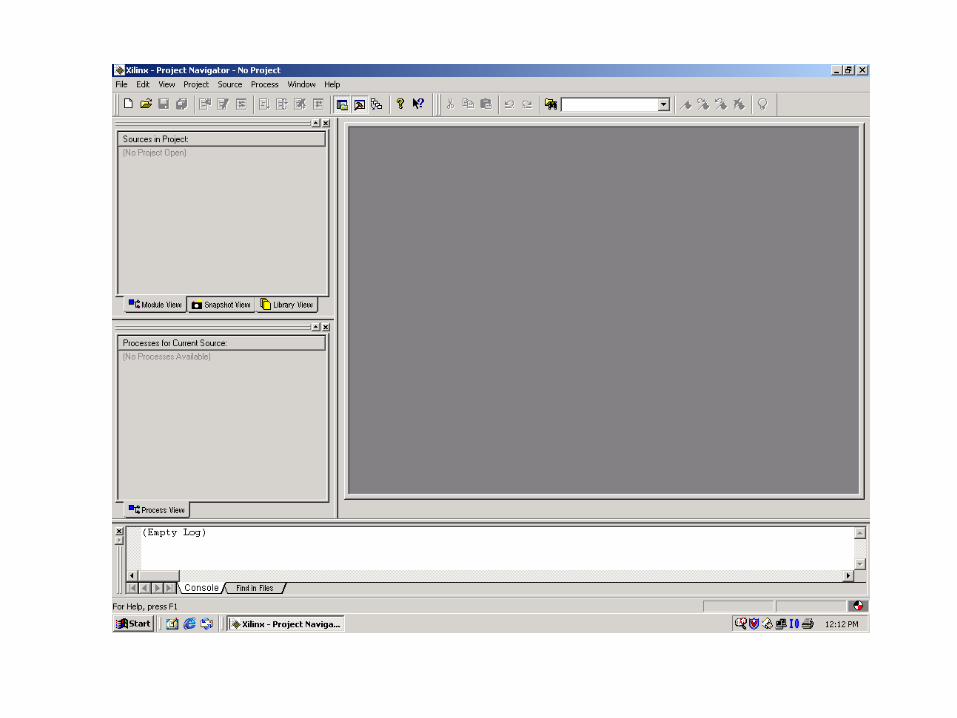

Click on the FILE menu and select New Project.

Name the New Project as follows. Change the VALUES accordingly.

The following window appears on your screen……

Right click on XCV…….. and select New Source.
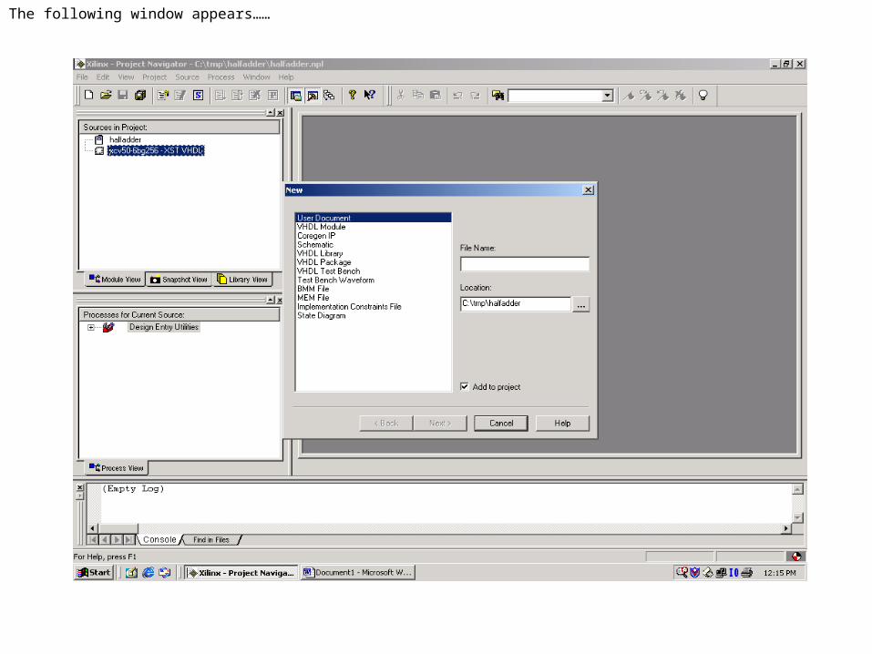
The following window appears……
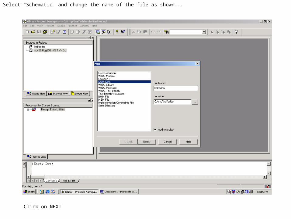
Select “Schematic” and change the name of the file as shown…..
Click on NEXT
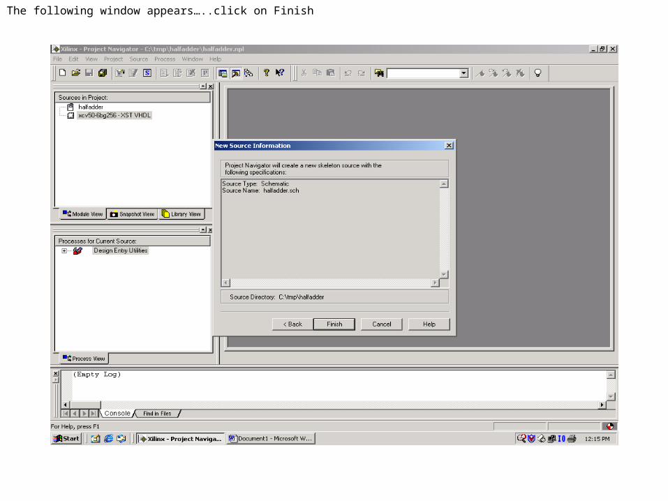
The following window appears…..click on Finish

The following window opens up:
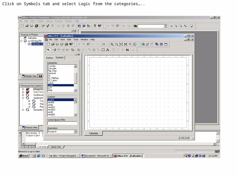
Click on Symbols tab and select Logic from the categories…..
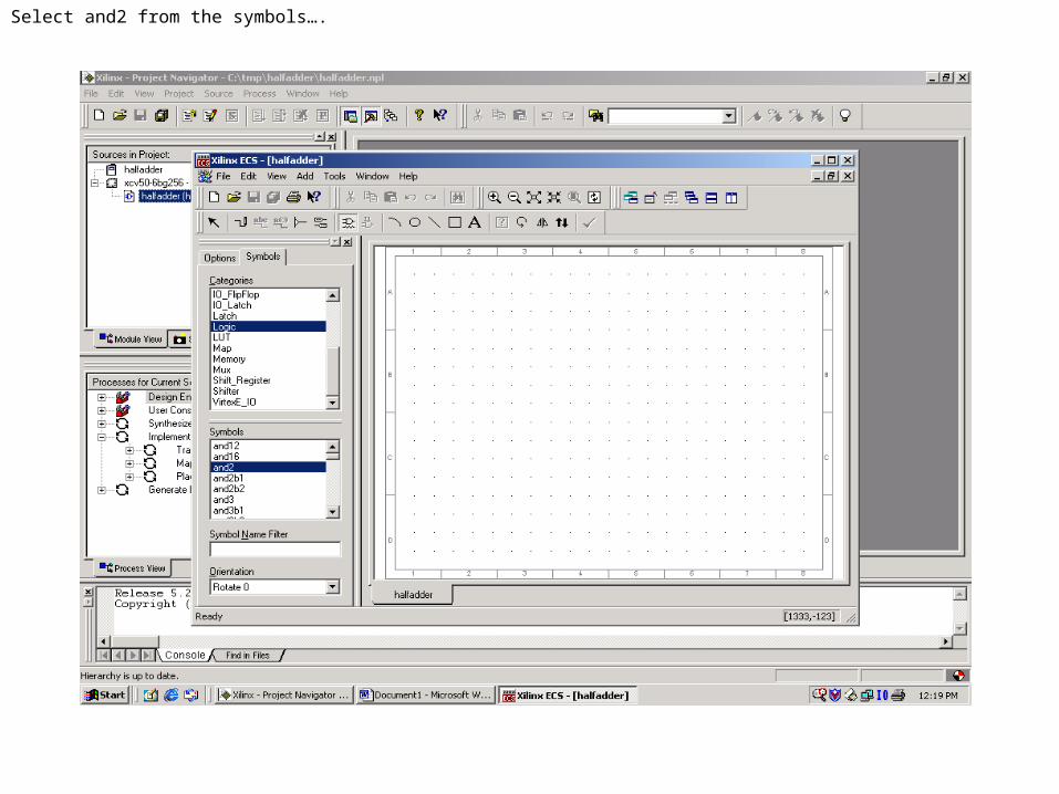
Select and2 from the symbols….

Place the 2-input AND gate on the schematic window as shown:
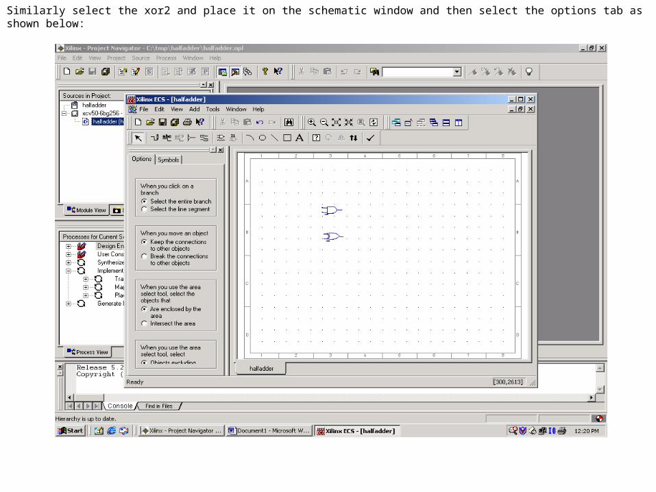
Similarly select the xor2 and place it on the schematic window and then select the options tab as shown below:

Click the “Add Wire” button as shown:
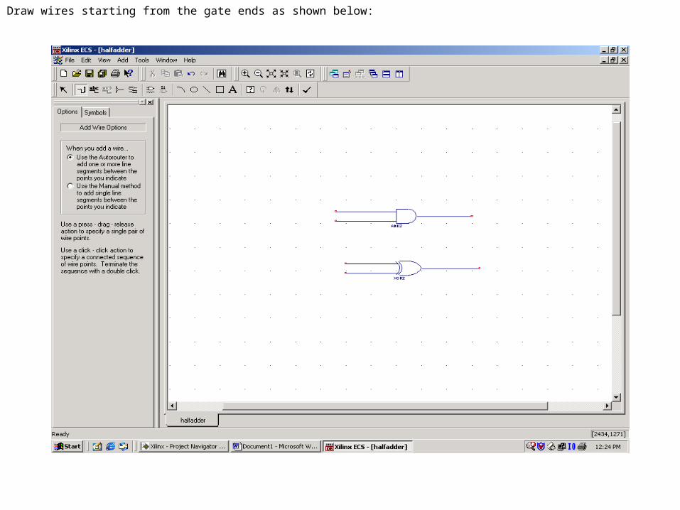
Draw wires starting from the gate ends as shown below:

Click on the “Add I/O Marker” and select the “Add input marker” option in the options tab as shown….

Place the two pins as shown :
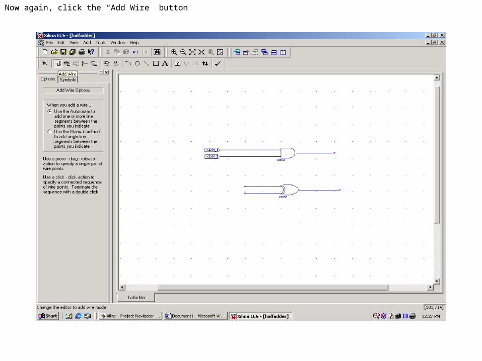
Now again, click the “Add Wire” button
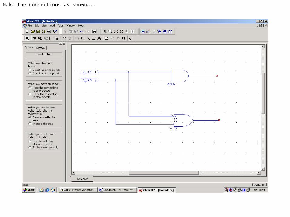
Make the connections as shown…..

Right click on the XLXN_1 pin and select Rename

The following window appears….
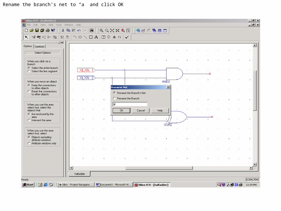
Rename the branch’s net to “a” and click OK

Follow the above procedure to rename the XLXN_2 pin to “b”
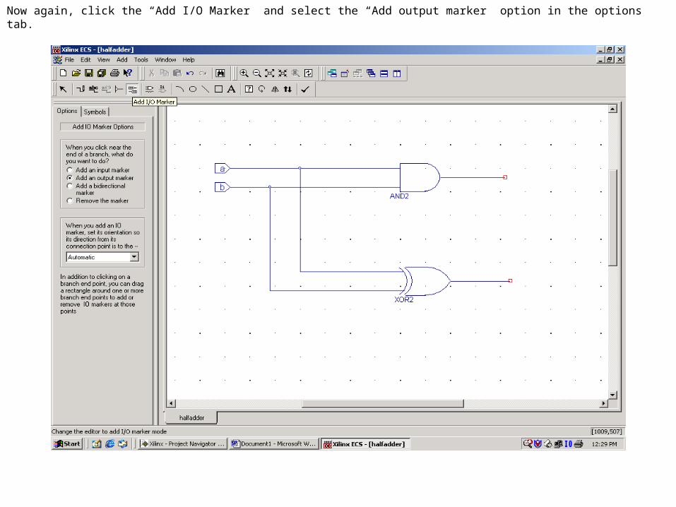
Now again, click the “Add I/O Marker” and select the “Add output marker” option in the options tab.

Place the pins as follows…..

Rename the output pins as follows….
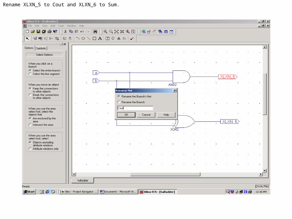
Rename XLXN_5 to Cout and XLXN_6 to Sum.

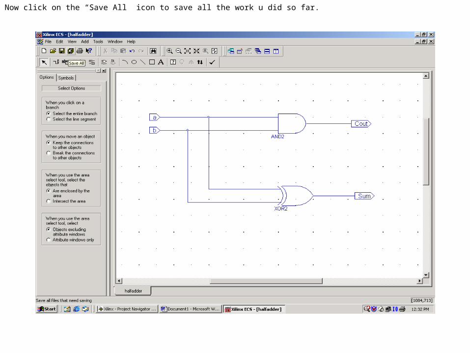
Now click on the “Save All” icon to save all the work u did so far.

In the main project navigator window, highlight the halfadder.sch as shown……
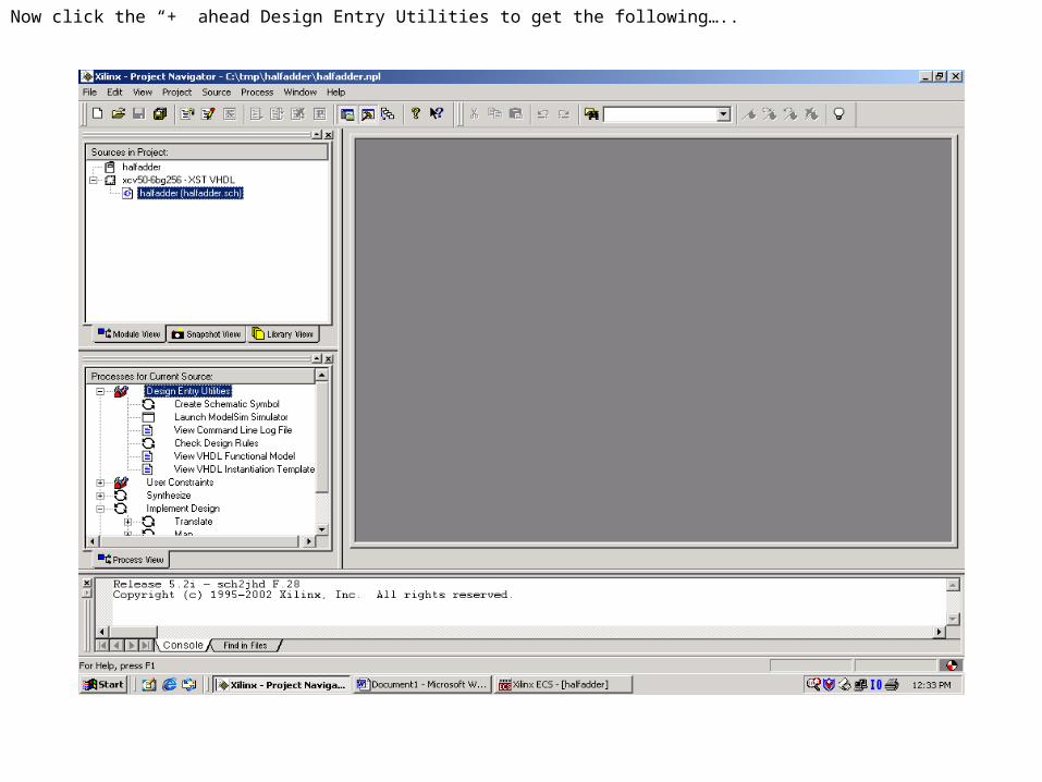
Now click the “+” ahead Design Entry Utilities to get the following…..

Select the Launch ModelSim Simulator and double click on it.
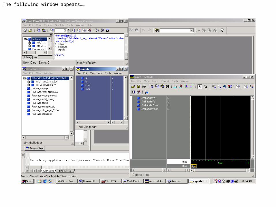
The following window appears……

In the signals window, highlight the signal “a” :
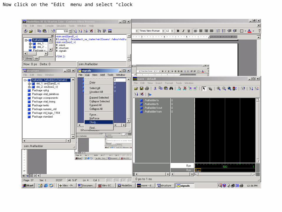
Now click on the “Edit” menu and select “clock”

In the “define clock window” , change the period to 1000 (not 100 )
Period = 1000

Do the same for signal “b” but change the period to 2000(not 200)
Period = 2000 Click OK.
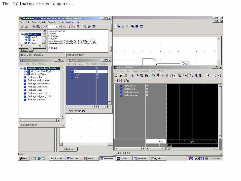
The following screen appears….

Maximize the Wave-Default window and click on RUN as shown…

The following waveform appears. Place the cursor accordingly to check for the correct output values for all combinations of “a” and “b”. there is a delay of 100ps which you can ignore while checking for the output values.


