32
MIDI Receiver in Verilog Professor Daniel Holcomb UMass Amherst Fall 2016 ECE 353 Lab 4

MIDI Receiver in Verilog
Professor Daniel Holcomb UMass Amherst
Fall 2016
ECE 353 Lab 4

Computer Systems Lab 1 UMass2
Timeline and Grading for Lab 4▪ Lectures on 11/15 and 11/17 ▪ Due on 12/12
▪ Demos in Duda hall ▪ Schedule will be posted online, sign up for slots
▪ Lab assessments (on course webpage) ▪ Completed by students before checkoff ▪ Completed by us at demo
▪ Report ▪ Submitted on Moodle by 11:55pm on due date ▪ Also submit Verilog code with comments ▪ More details in assignment ▪ Be concise

Computer Systems Lab 1 UMass3
Lab 4 Resources▪ My office hours (Tu/Th 10-11) ▪ My informal Q&A sessions in Duda hall (Tu/Th 1-2:15)
▪ TA office hours in Duda hall (M-F 7-9)
▪ Video demonstration on course website to show how to use Quartus software to program CPLD ▪ Simple demo code on website
▪ Resources on website (and elsewhere) for Verilog

Computer Systems Lab 1 UMass4
Software vs Hardware▪ Lab 2: microcontroller software to perform low-level control of
ATmega32 USART module ▪ SW: C code gets compiled to machine instructions that
dynamically control the hardware as it runs
▪ Lab 4: your own hardware implementation of the USART’s receive function ▪ HW: Verilog code gets compiled to bitstream that statically
configures the logic function of the hardware

Computer Systems Lab 1 UMass5
Hardware Design▪ Moore’s law: ICs have gone from
hundreds of transistors per chip to billions per chip in 50 years
▪ The methodology for designing hardware has also changed ▪ Automation and abstractions to
manage scale and complexity
Kilby’s IC, from wikipedia http://download.intel.com/newsroom/kits/core/6thgen/gallery/images/6th_Gen_Intel_Core_die_flat.jpg
Computer Systems Lab 1 UMass6
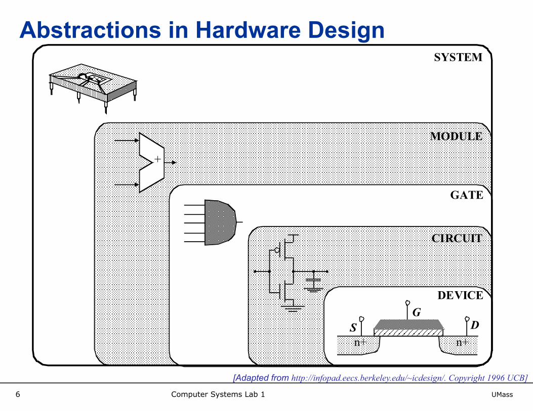
Abstractions in Hardware Design
n+n+S
GD
+
DEVICE
CIRCUIT
GATE
MODULE
SYSTEM
[Adapted from http://infopad.eecs.berkeley.edu/~icdesign/. Copyright 1996 UCB]

Computer Systems Lab 1 UMass7
Implementing Digital Hardware▪ Digital hardware comprises sequential and combinational logic ▪ How to create?
▪ Using discrete logic gates on breadboard ▪ limited to a few gates and flip-flops ▪ slow
▪ Programmable logic ▪ Thousands - millions of generic gate-equivalents and flip-flops ▪ up to ~200 MHz ▪ This lab uses a low-end programmable logic device (vs FPGA)
▪ ASIC: application-specific integrated circuit ▪ thousands - billions of gates and flip flops ▪ up to ~4Ghz
▪ Complexity of hardware necessitates automation ▪ Hardware Description Languages such as Verilog and VHDL ▪ HDL is the same regardless of whether target is programmable logic or
ASIC

Computer Systems Lab 1 UMass8
Why Programmable Logic?▪ Cost is one reason
▪ ASIC: application-specific integrated circuit ▪ Huge fixed cost (lithography masks, engineers) ▪ Lowest variable cost (most efficient use of chip area) ▪ Only cost-effective for large quantities
▪ Programmable logic is an ASIC from the producer’s perspective ▪ Generality of the design enables large quantities to be sold
▪ Programmable logic from perspective of implementer: ▪ Sharing the fixed cost across all other implementers who use the
same programmable logic ▪ Incremental cost is higher than ASIC due to less efficient use of chip
area ▪ Given fixed costs and variable costs, find quantity needed to justify ASIC
cost_per_unit = variable_cost + fixed_cost/quantity
Computer Systems Lab 1 UMass9
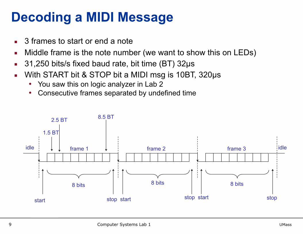
Decoding a MIDI Message▪ 3 frames to start or end a note ▪ Middle frame is the note number (we want to show this on LEDs) ▪ 31,250 bits/s fixed baud rate, bit time (BT) 32µs ▪ With START bit & STOP bit a MIDI msg is 10BT, 320µs
• You saw this on logic analyzer in Lab 2 • Consecutive frames separated by undefined time
idle
1.5 BT
idle
8.5 BT
stop startstart
8 bits
stop start stop
8 bits 8 bits
2.5 BT
frame 3frame 2frame 1

Computer Systems Lab 1 UMass10
Inspiration for Lab 4 Design: A Closer Look at Hardware of ATMega32 USART receiver

Computer Systems Lab 1 UMass11
ATmega32: Decoding of a MIDI Message
Computer Systems Lab 1 UMass12
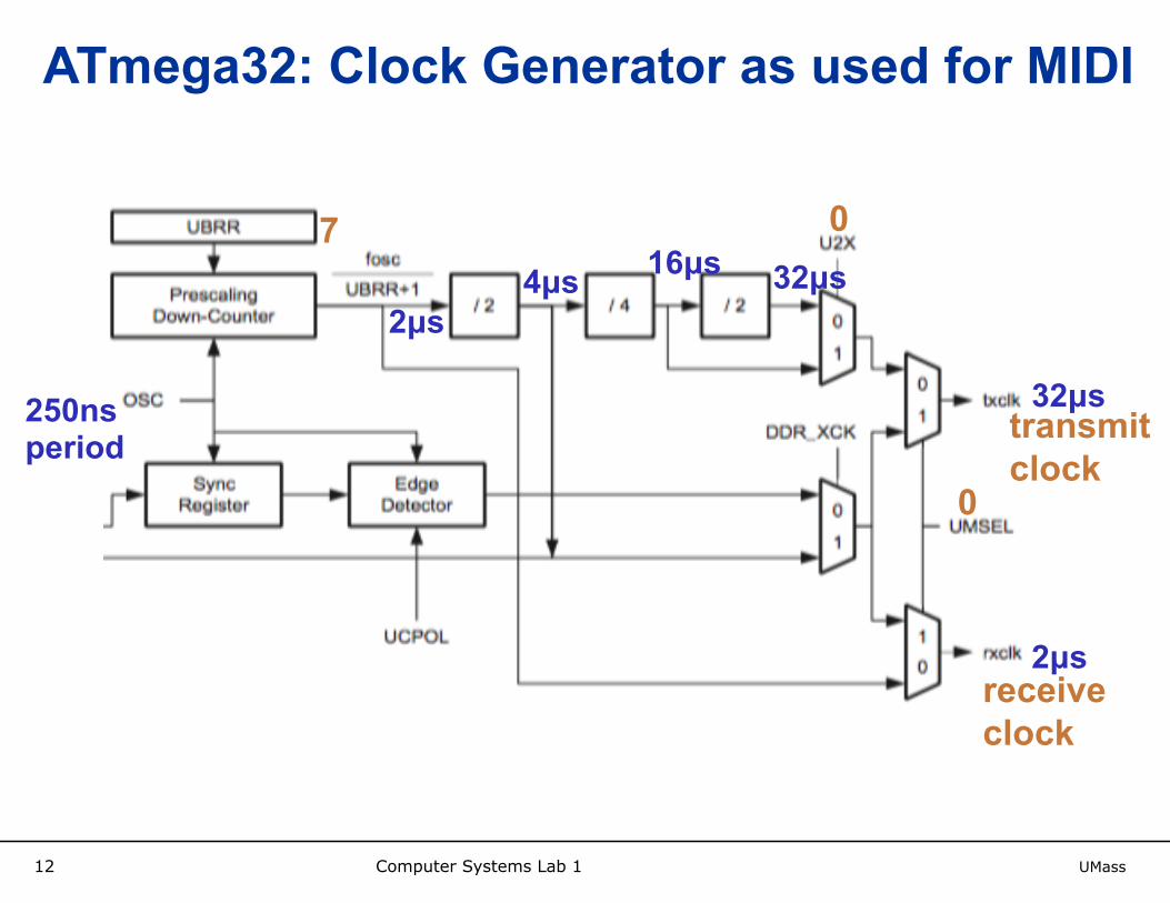
ATmega32: Clock Generator as used for MIDI
07
250ns period
2µs4µs 16µs 32µs
32µs
2µs
0
receive clock
transmit clock

Computer Systems Lab 1 UMass13
ATmega32: Sampling Rx Data Line in USART▪ Start of frame detected by falling data line (indicates beginning of start
bit) ▪ Comparing previous value to current value (using 2µs clock) ▪ First receive clock tick could be misaligned by 2µs
▪ 16 ticks of (2µs) receive clock per bit ▪ USART samples data line 3 times in the middle of the bit and does
majority voting for robustness ▪ In Lab 4 can sample just once, but be sure to sample middle of bit
1 0rx clock
data

Computer Systems Lab 1 UMass14
Technical Description of Lab 4
Computer Systems Lab 1 UMass15
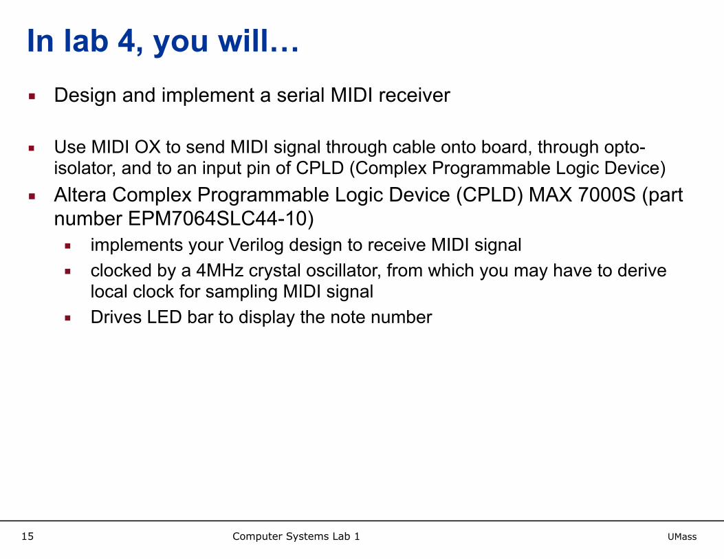
In lab 4, you will…▪ Design and implement a serial MIDI receiver
▪ Use MIDI OX to send MIDI signal through cable onto board, through opto-isolator, and to an input pin of CPLD (Complex Programmable Logic Device)
▪ Altera Complex Programmable Logic Device (CPLD) MAX 7000S (part number EPM7064SLC44-10) ▪ implements your Verilog design to receive MIDI signal ▪ clocked by a 4MHz crystal oscillator, from which you may have to derive
local clock for sampling MIDI signal ▪ Drives LED bar to display the note number
Computer Systems Lab 1 UMass16
In lab 4, you will learn about…▪ Programming hardware in Verilog ▪ Using Altera Quartus II 9.1 software tools for synthesis ▪ Debugging design with functional simulation (waveforms) ▪ Wiring up circuit on breadboard ▪ Debugging and testing board with logic analyzer

Computer Systems Lab 1 UMass17
Sampling of MIDI frames▪ Board has a 4MHz clock that you need to divide (or count) ▪ Before a frame, input signal idles high ▪ When idle, detect negative edge of MIDI line for start bit ▪ Now start sampling 8 bits (payload) in the middle of each bit
• LSB at 1.5BT • … • MSB at 8.5BT • Stop bit is at 9.5 BT
▪ Repeat for each byte
idle
1.5 BT 8.5 BT
stopstart 8 bits
2.5 BT
frame

Computer Systems Lab 1 UMass18
Sampling of MIDI frames▪ Real MIDI receivers would implement a few features for robustness… ▪ Sampled value at 0.5BT is not logic 0?
▪ Falling transition was probably a glitch and not a start bit ▪ Sampled value at 9.5BT is not logic 1?
▪ A MIDI receiver sets a flag “Framing Error” ▪ You can implement if you want (not required)
▪ Sampling multiple times per bit and voting on bit value ▪ Triple Modulo Redundancy (TMR) voter would vote majority of 3 samples
▪ You don’t need to implement these extra features
idle
1.5 BT 8.5 BT
stopstart 8 bits
2.5 BT
frame

Computer Systems Lab 1 UMass19
Programming Header
MIDI signal (referenced to breadboard GND)
Configuration Bitstream
MIDI Signal/Cable (output from MIDI-OX)
LEDs/resistors
CPLD Implements
Design
USB Blaster Programmer Cable (from Quartus II)
Hardware outside line is same as lab 2
choose any pins for i/o
reset button
Computer Systems Lab 1 UMass21
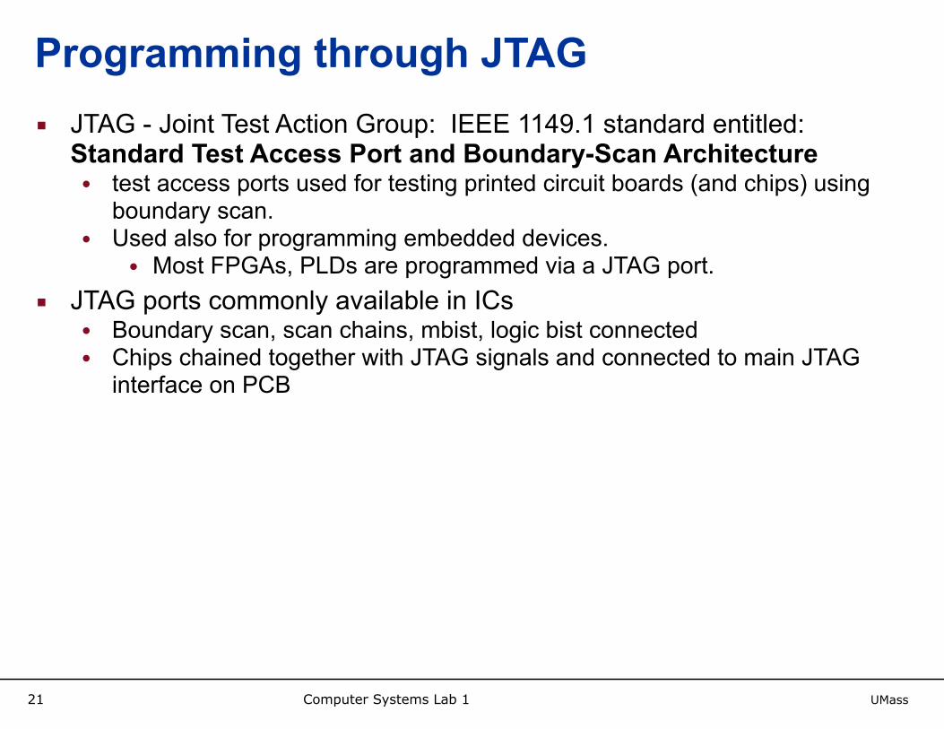
Programming through JTAG▪ JTAG - Joint Test Action Group: IEEE 1149.1 standard entitled:
Standard Test Access Port and Boundary-Scan Architecture • test access ports used for testing printed circuit boards (and chips) using
boundary scan. • Used also for programming embedded devices.
• Most FPGAs, PLDs are programmed via a JTAG port. ▪ JTAG ports commonly available in ICs
• Boundary scan, scan chains, mbist, logic bist connected • Chips chained together with JTAG signals and connected to main JTAG
interface on PCB

Computer Systems Lab 1 UMass22
Building project▪ Board Assembly (reuse much of Lab 2) ▪ Implementing your design
▪ Plan modules (design must include multiple modules) ▪ Write Verilog HDL ▪ Synthesis ▪ Simulation (test/debug) ▪ Load the configuration onto the CPLD
▪ Testing ▪ MIDI-OX ▪ Logic Analyzer
Computer Systems Lab 1 UMass23
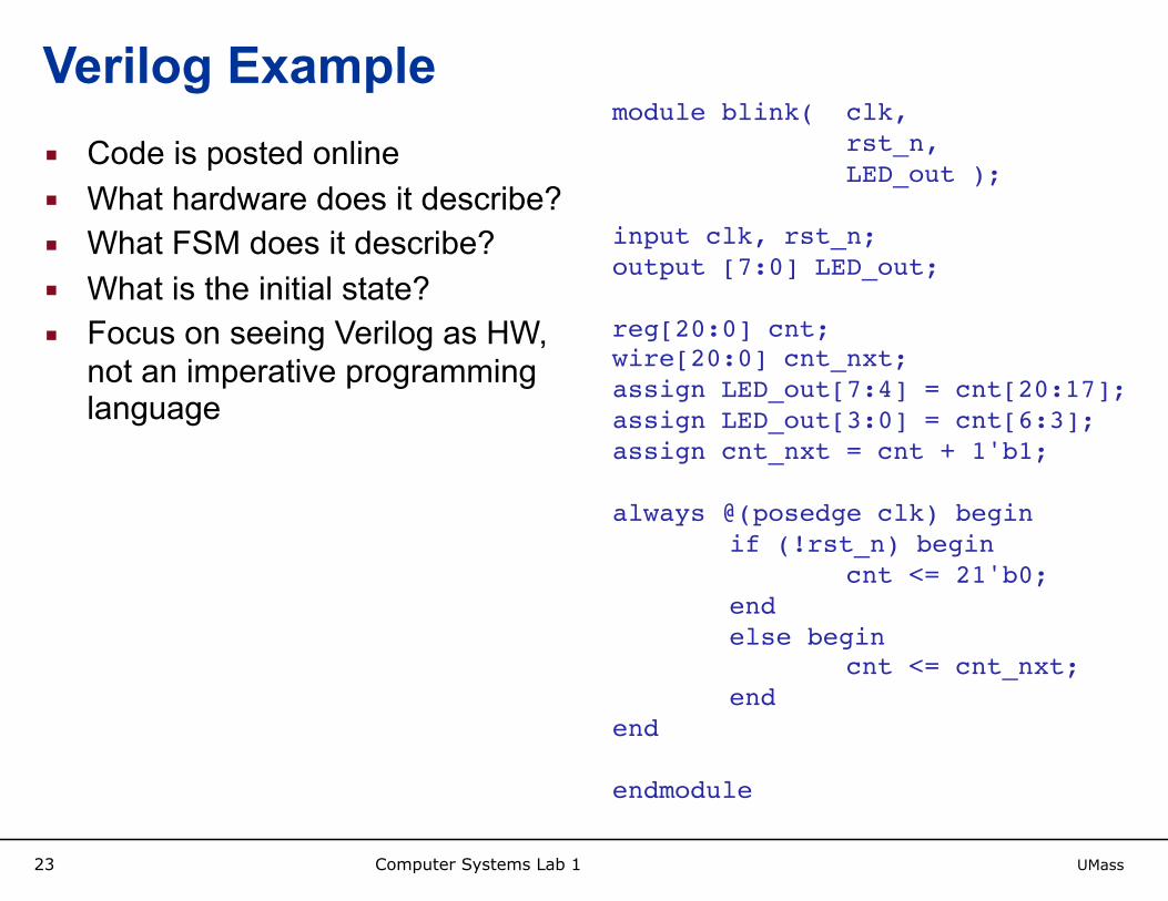
Verilog Example▪ Code is posted online ▪ What hardware does it describe? ▪ What FSM does it describe? ▪ What is the initial state? ▪ Focus on seeing Verilog as HW,
not an imperative programming language
module blink( clk, rst_n, LED_out );
input clk, rst_n;output [7:0] LED_out;
reg[20:0] cnt;wire[20:0] cnt_nxt;assign LED_out[7:4] = cnt[20:17];assign LED_out[3:0] = cnt[6:3]; assign cnt_nxt = cnt + 1'b1;
always @(posedge clk) beginif (!rst_n) begin
cnt <= 21'b0;endelse begin
cnt <= cnt_nxt;end
end
endmodule
Computer Systems Lab 1 UMass24
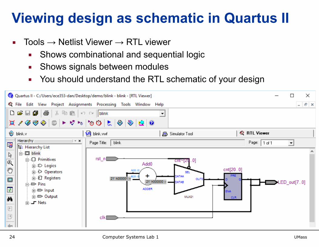
Viewing design as schematic in Quartus II▪ Tools → Netlist Viewer → RTL viewer
▪ Shows combinational and sequential logic ▪ Shows signals between modules ▪ You should understand the RTL schematic of your design

Computer Systems Lab 1 UMass25
Metastability▪ Incoming MIDI signal is captured by flip flop, but is asynchronous w.r.t. system clock ▪ What happens if signal changes at same time as clock?
▪ Setup time violation ▪ Can cause metastability: flip-flop output stuck between 0 and 1 ▪ Will eventually resolve to either 0 or 1, but may take a while ▪ Metastability is non-digital behavior and should be avoided
▪ Prevent this using double-sampling by two flip-flop in sequence ▪ FF2 will not be metastable unless FF1 metastable through entire clock period
https://www.altera.com/content/dam/altera-www/global/en_US/pdfs/literature/wp/wp-01082-quartus-ii-metastability.pdfhttp://www.interfacebus.com/Design_MetaStable.html

Computer Systems Lab 1 UMass26
Design in Verilog▪ Review of Verilog is provided in next lecture ▪ Focus is on methodology for proper design and coding ▪ See also many good resources online for Verilog coding

Computer Systems Lab 1 UMass27
Tool flow for configuring CPLD to implement your design
Computer Systems Lab 1 UMass28
Overview
▪ Instructions in the next slides explain how to implement a Verilog design on CPLD
▪ First follow these instructions using the “blink.v” code from the course webpage ▪ Video linked on course webpage shows screen
capture of following these instructions in Quartus
▪ Once you’ve done this successfully for the example code, then start the process over using your own code

Computer Systems Lab 1 UMass29
Creating the Project▪ Open Quartus II 9.1 and create new project
▪ Page 1: Name project appropriately ▪ Page 2: Nothing (will add your source files later) ▪ Page 3:
▪ Family: MAX7000S ▪ Name: EPM7064SLC44-10
▪ Page 4: Nothing (using default tools) ▪ Page 5: Finish
▪ Now empty project is created
Computer Systems Lab 1 UMass30
Add Verilog File to Project▪ File → new → Verilog HDL file
▪ Write some verilog code (or paste blink.v) ▪ Save file, notice check box for “add to project” while saving
▪ Start Compilation – Purple arrow ▪ This elaborates and synthesizes your design ▪ Take note of any warnings ▪ Some can be ignored, some cause problems ▪ Come back to these if your design doesn’t work right
▪ Now your design is synthesized

Computer Systems Lab 1 UMass31
Pin Assignment▪ This sets correspondence between input and output signals of
your design and the specific pins of the chip ▪ Assignments → Pin Planner
▪ Make sure you have right chip ▪ Picture shows the layout (top view) of your chip ▪ Decide which signals you want to have on each pin ▪ Some pins have dedicated signals ▪ Double-click pin and select the signal that you want to
assign to that pin ▪ When finished, close pin planner and recompile

Computer Systems Lab 1 UMass32
Waveform Simulation▪ Test design in simulation before putting on board ▪ Functional simulation using Vector Waveform Files ▪ File → new → Vector Waveform File
▪ Edit → end time: set end time ▪ Add nodes to VWF, provide waveforms for input nodes ▪ This will be input stimulus for simulation ▪ Save and add to project
▪ Processing → Simulator Tool ▪ Select functional simulation and then generate functional simulation
netlist ▪ Select overwrite simulation input file with results ▪ Click start, then open ▪ Waveforms are now updated to show the response of system to the
inputs ▪ Note, can observe internal signals for debugging too (i.e. not just outputs)
▪ Make sure your design simulates properly before moving on!

Computer Systems Lab 1 UMass33
Load Design onto Chip▪ Tools → Programmer
▪ Using USB blaster to load bitstream onto device ▪ Check connection/settings, click start wait for 100% ▪ Now your design is running on CPLD
▪ Note: if installing the USB blaster driver on your own computer ▪ Need to install driver from lab CD (or can find online) ▪ By default windows won’t install driver if it cannot verify
authenticity. Can fix by adjusting Windows settings ▪ Non-windows users can do this all in a VirtualBoxVM
▪ On the lab computers, everything should be already installed


