Page 1
Lecture Notes Page 2.1ECE 410, Prof. F. Salem
ECE 410: VLSI DesignCourse Lecture Notes
(Uyemura textbook)
Professor Fathi Salem
Michigan State University
We will be updating the notes this Semester.
Page 2
Lecture Notes Page 2.2ECE 410, Prof. F. Salem
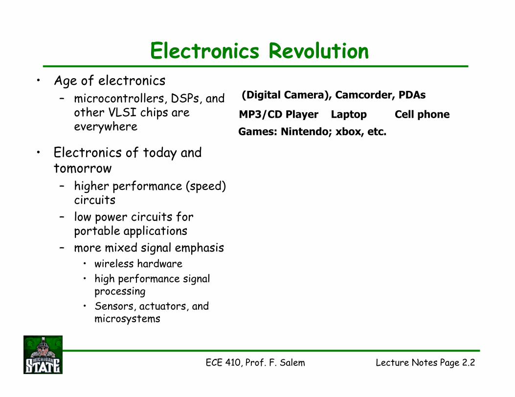
Electronics Revolution• Age of electronics
– microcontrollers, DSPs, and other VLSI chips are everywhere
• Electronics of today and tomorrow– higher performance (speed)
circuits
– low power circuits for portable applications
– more mixed signal emphasis• wireless hardware
• high performance signal processing
• Sensors, actuators, and microsystems
(Digital Camera), Camcorder, PDAs
MP3/CD Player Laptop Cell phone
Games: Nintendo; xbox, etc.
Page 3
Lecture Notes Page 2.3ECE 410, Prof. F. Salem
Figure 1.1 (p. 2)The VLSI design
funnel.
Page 4
Lecture Notes Page 2.4ECE 410, Prof. F. Salem
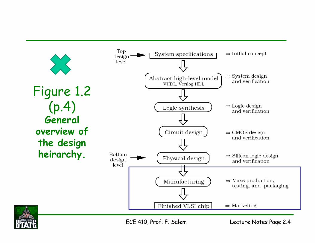
Figure 1.2 (p.4)
General overview of the design heirarchy.
Page 5
Lecture Notes Page 2.5ECE 410, Prof. F. Salem
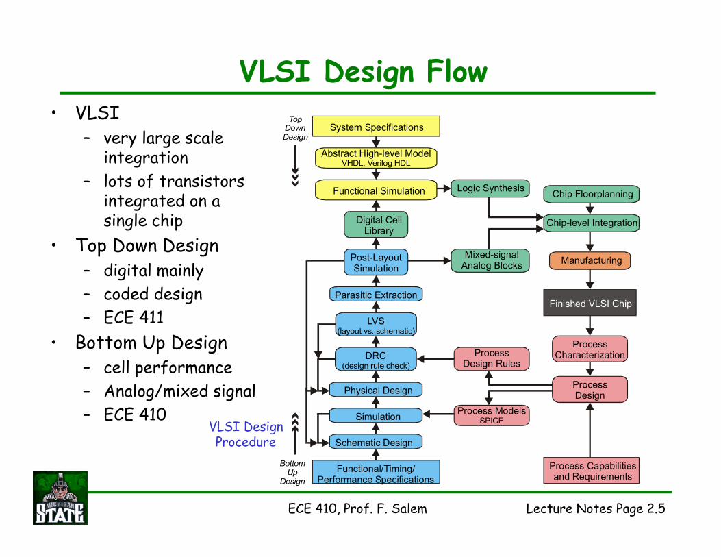
VLSI Design Flow• VLSI
– very large scale integration
– lots of transistors integrated on a single chip
• Top Down Design– digital mainly
– coded design
– ECE 411
• Bottom Up Design– cell performance
– Analog/mixed signal
– ECE 410VLSI DesignProcedure
System Specifications
Logic SynthesisChip Floorplanning
Chip-level Integration
Manufacturing
Finished VLSI Chip
Schematic Design
LVS(layout vs. schematic)
Parasitic Extraction
Post-LayoutSimulation
Digital CellLibrary
Mixed-signalAnalog Blocks
DRC(design rule check)
Simulation
Physical Design
Process ModelsSPICE
ProcessCharacterization
ProcessDesign
Process Capabilitiesand Requirements
ProcessDesign Rules
Abstract High-level ModelVHDL, Verilog HDL
TopDownDesign
BottomUp
Design
Functional Simulation
Functional/Timing/Performance Specifications
Page 6
Lecture Notes Page 2.6ECE 410, Prof. F. Salem
Integrated Circuit Technologies• Why does CMOS dominate--Now?
– other technologies• passive circuits• III-V devices• Silicon BJT
• CMOS dominates because:– Silicon is cheaper � preferred over other materials– physics of CMOS is easier to understand???– CMOS is easier to implement/fabricate– CMOS provides lower power-delay product– CMOS is lowest power– can get more CMOS transistors/functions in same chip area
• BUT! CMOS is not the fastest technology!– BJT and III-V devices are faster
Page 7
Lecture Notes Page 2.7ECE 410, Prof. F. Salem
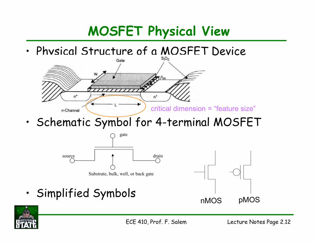
• Physical Structure of a MOSFET Device
• Schematic Symbol for 4-terminal MOSFET
• Simplified Symbols
MOSFET Physical View
source drain
Substrate, bulk, well, or back gate
gate
nMOS pMOS
critical dimension = “feature size”
Page 8
Lecture Notes Page 2.8ECE 410, Prof. F. Salem
CMOS Technology Trends
• Variations over time– # transistors / chip: increasing with time
– power / transistor: decreasing with time (constant power density)
– device channel length: decreasing with time
– power supply voltage: decreasing with time
ref: Kuo and Lou, Low-Voltage CMOS VLSI Circuits, Fig. 1.3, p. 3
transistors /
chip
power /
transistor
channel length
supply voltage
low power/transistor is critical for future ICs
Page 9
Lecture Notes Page 2.9ECE 410, Prof. F. Salem
Moore’s Law• In 1965, Gordon Moore realized there
was a striking trend; each new generation of memory chip contained roughly twice as much capacity as its predecessor, and each chip was released within 18-24 months of the previous chip. He reasoned, computing power would rise exponentially over relatively brief periods of time.
• Moore's observation, now known as Moore's Law, described a trend that has continued and is still remarkably accurate. In 26 years the number of transistors on a chip has increased more than 3,200 times, from 2,300 on the 4004 in 1971 to 7.5 million on the Pentium¨ II processor.
10µm 1µm 0.35µm 45 nm
(ref: http://www.intel.com/intel/museum/25anniv/hof/moore.htm)Feature Size
180 130 90 60 40 30Feature Size (nm)1999 2001 2004 2008 2011 2014
1.8 V
1.5 V
1.2 V
0.9 V
0.6 V 0.6 V
Year
Power Supply Tends
Digital Core Voltage Projectionsfrom the 2000 ITRS*
* http://public.itrs.net/Files/2000UpdateFinal/ORTC2000final.pdf
2 Billion
Page 10
Lecture Notes Page 2.10ECE 410, Prof. F. Salem
• MOSFET Device-- 1950+ to 2020
• New elements in nano technologies are emerging. These include: – Fin-Transistor
– Memristor: memory resistor- see IEEE Spectrum
– Nano-tubes
– Molecular devices
– Quantum dots
– Etc.
“Electronics” Building block(s)
Page 11
Lecture Notes Page 2.11ECE 410, Prof. F. Salem
VLSI Design Flow• VLSI
– very large scale integration
– lots of transistors integrated on a single chip
• Top Down Design– digital mainly
– coded design
– ECE 411
• Bottom Up Design– cell performance
– Analog/mixed signal
– ECE 410VLSI DesignProcedure
System Specifications
Logic SynthesisChip Floorplanning
Chip-level Integration
Manufacturing
Finished VLSI Chip
Schematic Design
LVS(layout vs. schematic)
Parasitic Extraction
Post-LayoutSimulation
Digital CellLibrary
Mixed-signalAnalog Blocks
DRC(design rule check)
Simulation
Physical Design
Process ModelsSPICE
ProcessCharacterization
ProcessDesign
Process Capabilitiesand Requirements
ProcessDesign Rules
Abstract High-level ModelVHDL, Verilog HDL
TopDownDesign
BottomUp
Design
Functional Simulation
Functional/Timing/Performance Specifications
Page 12
Lecture Notes Page 2.12ECE 410, Prof. F. Salem
• Physical Structure of a MOSFET Device
• Schematic Symbol for 4-terminal MOSFET
• Simplified Symbols
MOSFET Physical View
source drain
Substrate, bulk, well, or back gate
gate
nMOS pMOS
critical dimension = “feature size”
Page 13
Lecture Notes Page 2.13ECE 410, Prof. F. Salem
What is a MOSFET?• Digital integrated circuits rely on transistor switches
– most common device for digital and mixed signal: MOSFET
• Definitions– MOS = Metal Oxide Semiconductor
• physical layers of the device
– FET = Field Effect Transistor
• What field? What does the field do?
• Are other fields important?
– CMOS = Complementary MOS
• use of both nMOS and pMOS to form
a circuit with lowest power consumption.
• Primary Features– gate; gate oxide (insulator)– very thin (~10^(-10))-- exaggerated in Fig.– source and drain– channel– bulk/substrate
Poly
OxideEEEE
V
gate
insulator
silicon substrate
drain- - - - - - - - - - - -channel
source
Semi-
conductor
NOTE: “Poly” stands for polysilicon in modern MOSFETs
Page 14
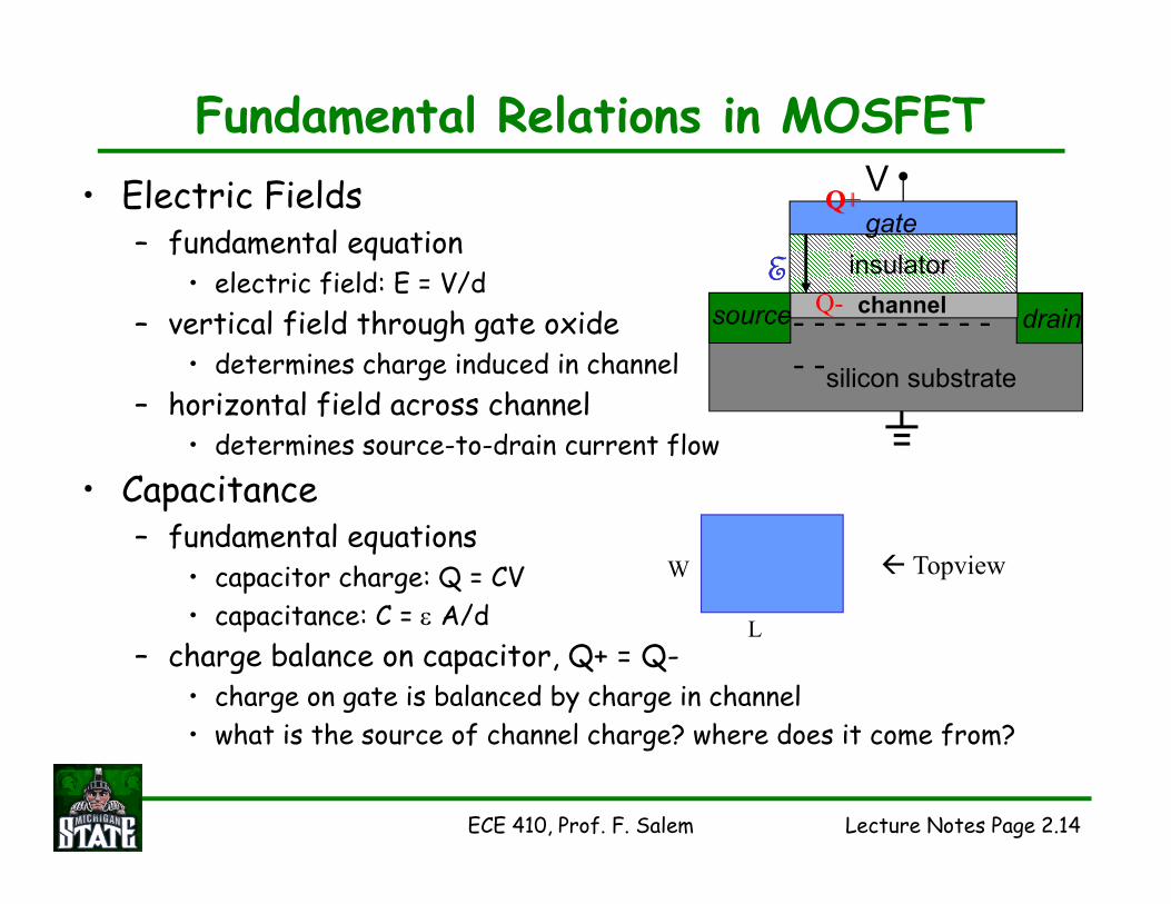
Lecture Notes Page 2.14ECE 410, Prof. F. Salem
Fundamental Relations in MOSFET
• Electric Fields– fundamental equation
• electric field: E = V/d
– vertical field through gate oxide• determines charge induced in channel
– horizontal field across channel• determines source-to-drain current flow
• Capacitance– fundamental equations
• capacitor charge: Q = CV
• capacitance: C = ε A/d
– charge balance on capacitor, Q+ = Q-• charge on gate is balanced by charge in channel
• what is the source of channel charge? where does it come from?
EEEE
Vgate
insulator
silicon substrate
drain- - - - - - - - - -
- -
channelsource
Q+Q+
Q-
W
L
� Topview
Page 15
Lecture Notes Page 2.15ECE 410, Prof. F. Salem
CMOS Cross Section View• Cross section of a 2 metal, 1 poly CMOS process
• Layout (top view) of the devices above (partial, simplified)
Typical MOSFET Device (nMOS)
Page 16
Lecture Notes Page 2.16ECE 410, Prof. F. Salem
CMOS Circuit Basics
nMOS
gategate
drain
source
source
drain
pMOS
• CMOS = complementary MOS
– uses 2 types of MOSFETs
to create logic functions
• nMOS
• pMOS
• CMOS Power Supply
– typically single power supply
– VDD, with Ground reference
• typically uses single power supply
• VDD ranges from (0.6V) 1V to 5V
• Logic Levels (voltage-based)
– all voltages between 0V and VDD
– Logic ‘1’ = VDD
– Logic ‘0’ = ground = 0V
+-VDD
VDD
=CMOSlogiccircuit
CMOSlogiccircuit
VVDD
logic 1
voltages
logic 0
voltages
undefined
Page 17
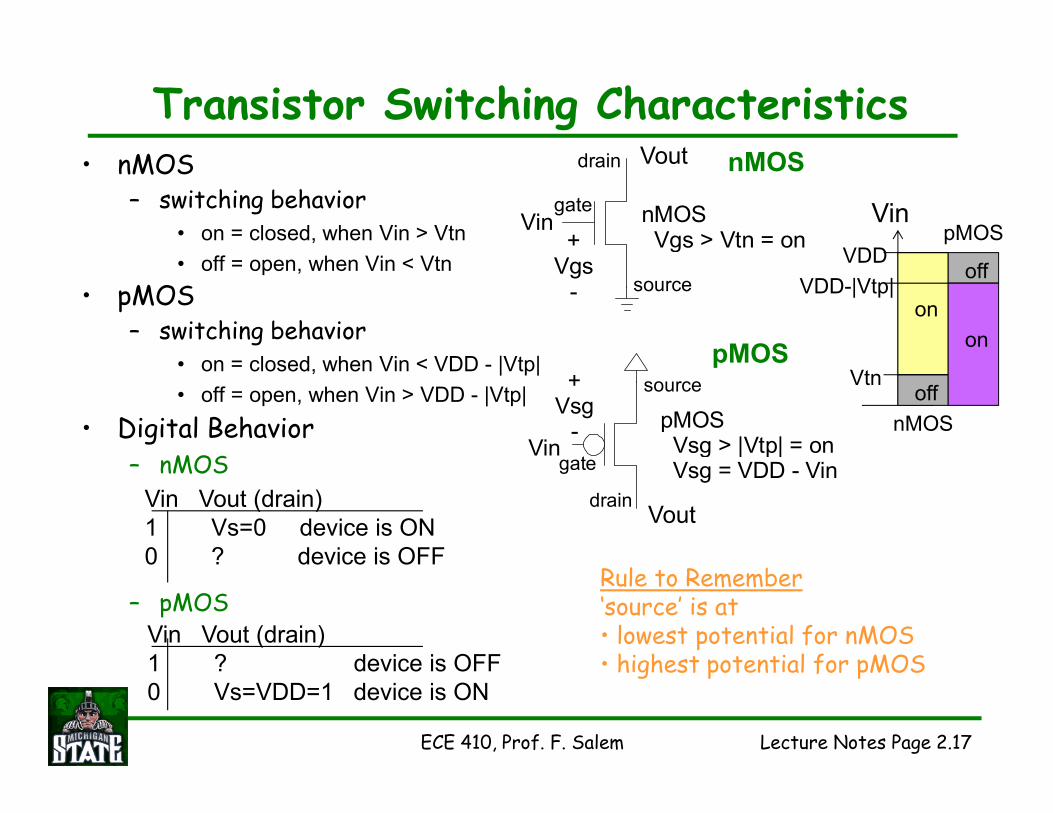
Lecture Notes Page 2.17ECE 410, Prof. F. Salem
Transistor Switching Characteristics• nMOS
– switching behavior• on = closed, when Vin > Vtn
• off = open, when Vin < Vtn
• pMOS– switching behavior
• on = closed, when Vin < VDD - |Vtp|
• off = open, when Vin > VDD - |Vtp|
• Digital Behavior– nMOS
– pMOS
pMOS
nMOS
nMOS Vgs > Vtn = on+
Vgs-
Vingate
drain
source
Vin
+Vsg
-
gate
source
drain
pMOS Vsg > |Vtp| = on Vsg = VDD - Vin
Rule to Remember‘source’ is at • lowest potential for nMOS• highest potential for pMOS
Vin
VDDpMOS
nMOS
VDD-|Vtp|
Vtn
on
off
off
on
Vin Vout (drain)
1 Vs=0 device is ON
0 ? device is OFF
Vin Vout (drain)
1 ? device is OFF
0 Vs=VDD=1 device is ON
Vout
Vout
Page 18
Lecture Notes Page 2.18ECE 410, Prof. F. Salem
MOSFET Pass Characteristics
nMOS
pMOS
Rule to Remember‘source’ is at lowest potential (nMOS) and highest potential (pMOS)
+Vgs=Vtn
-0 V VDD
VDD VDD
Vy = 0 V Vy =VDD-Vtn
-Vsg=|Vtp|
+VDD 0 V
0 V 0 V
Vy = VDD Vy = |Vtp|
on when gate is ‘low’
on when gate is ‘high’
Passes a good low
Max high is VDD-Vtn
Passes a good high
Min low is |Vtp|
• Each type of transistor is better at passing (to output) one digital voltage than the other– nMOS passes a good low (0) but not a good high (1)
– pMOS passes a good high (1) but not a good low (0)
Page 19
Lecture Notes Page 2.19ECE 410, Prof. F. Salem
MOSFET Terminal Voltages• How do you determine one terminal voltage if other 2 are known?
– nMOS• case 1) if Vg > Vi + Vtn, then Vo = Vi (Vg-Vi > Vtn)
– here Vi is the “source” so the nMOS will pass Vi to Vo
• case 2) if Vg < Vi + Vtn, then Vo = Vg-Vtn (Vg-Vi < Vtn)– here Vo is the “source” so the nMOS output is limited
• Example (Vtn=0.5V): Vg=5V, Vi=2V ⇒ Vo = 2V
Vg=2V, Vi=2V ⇒ Vo = 1.5V
– pMOS• case 1) if Vg < Vi - |Vtp|, then Vo = Vi (Vi-Vg > |Vtp|)
– here Vi is the “source” so the pMOS will pass Vi to Vo
• case 2) if Vg > Vi - |Vtp|, then Vo = Vg+|Vtp| (Vi-Vg < |Vtp|)– here Vo is the “source” so the pMOS output is limited
• Example (Vtp=-0.5V): Vg=2V, Vi=5V ⇒ Vo = 5V
Vg=2V, Vi=2V ⇒ Vo = 2.5V
Vg
Vo
Vi
Vg
Vo
Vi
For nMOS,
max(Vo) = Vg-Vtn
For pMOS,
min(Vo) = Vg+|Vtp|
Page 20
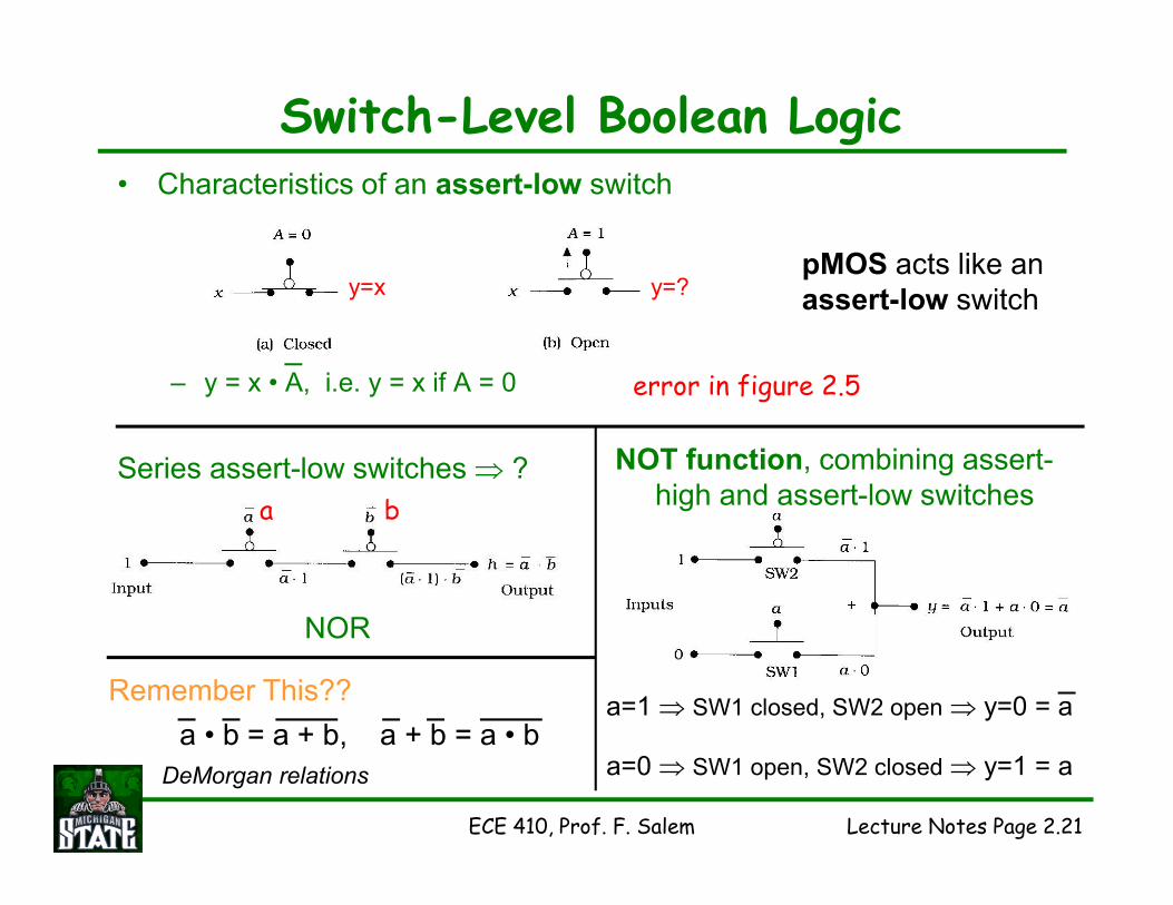
Lecture Notes Page 2.20ECE 410, Prof. F. Salem
Switch-Level Boolean Logic• Logic gates are created by using sets of controlled switches
• Characteristics of an assert-high switch
– y = x • A, i.e. y = x iff A = 1 (iff=if and only if)
Series switches ⇒ AND function Parallel switches ⇒ OR function
nMOS acts like an
assert-high switch=?
Page 21
Lecture Notes Page 2.21ECE 410, Prof. F. Salem
Switch-Level Boolean Logic• Characteristics of an assert-low switch
– y = x • A, i.e. y = x if A = 0
Series assert-low switches ⇒ ?
NOR
Remember This??
DeMorgan relations
a • b = a + b, a + b = a • ba=1 ⇒ SW1 closed, SW2 open ⇒ y=0 = a
a=0 ⇒ SW1 open, SW2 closed ⇒ y=1 = a
NOT function, combining assert-
high and assert-low switches
y=x y=?pMOS acts like an
assert-low switch
a b
error in figure 2.5
Page 22
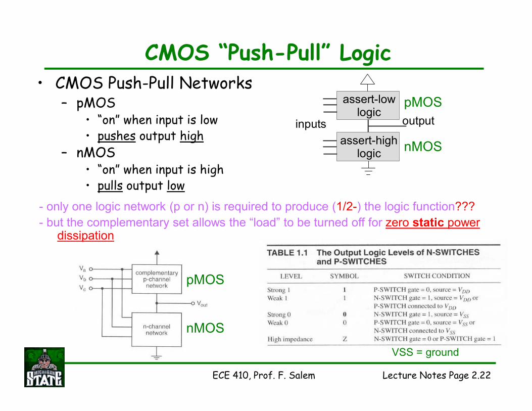
Lecture Notes Page 2.22ECE 410, Prof. F. Salem
CMOS “Push-Pull” Logic• CMOS Push-Pull Networks
– pMOS• “on” when input is low• pushes output high
– nMOS• “on” when input is high• pulls output low
pMOS
nMOS
- only one logic network (p or n) is required to produce (1/2-) the logic function???
- but the complementary set allows the “load” to be turned off for zero static power dissipation
pMOS
nMOS
assert-lowlogic
inputs output
assert-highlogic
VSS = ground
Page 23
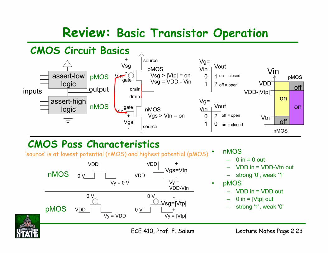
Lecture Notes Page 2.23ECE 410, Prof. F. Salem
Review: Basic Transistor Operation
CMOS Circuit Basics
• nMOS
– 0 in = 0 out
– VDD in = VDD-Vtn out
– strong ‘0’, weak ‘1’
• pMOS
– VDD in = VDD out
– 0 in = |Vtp| out
– strong ‘1’, weak ‘0’
assert-lowlogic
inputs output
assert-highlogic nMOS
Vgs > Vtn = on+Vgs
-
Vingate
drain
source
Vin
+Vsg
-
gate
source
drain
pMOS Vsg > |Vtp| = on Vsg = VDD - Vin
nMOS
pMOSVin
VDDpMOS
nMOS
Vtn
on
off
off
on
+Vgs=Vtn
-0 V VDD
VDD VDD
Vy = 0 V Vy =VDD-Vtn
-Vsg=|Vtp|
+VDD 0 V
0 V 0 V
Vy = VDD Vy = |Vtp|
CMOS Pass Characteristics
nMOS
pMOS
‘source’ is at lowest potential (nMOS) and highest potential (pMOS)
VDD-|Vtp|
Vg=
Vin Vout
?
0
0
1
Vg=
Vin Vout
1
?
0
1
off = open
on = closed
on = closed
off = open
Page 24
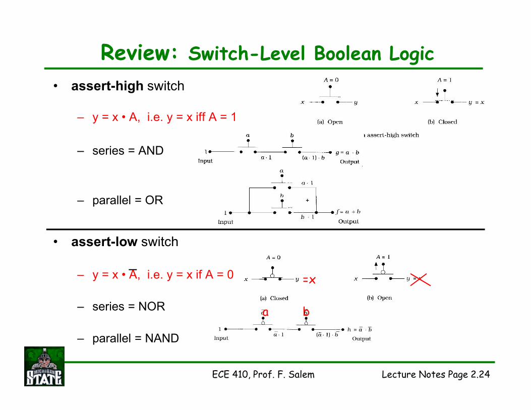
Lecture Notes Page 2.24ECE 410, Prof. F. Salem
Review: Switch-Level Boolean Logic
• assert-high switch
– y = x • A, i.e. y = x iff A = 1
– series = AND
– parallel = OR
• assert-low switch
– y = x • A, i.e. y = x if A = 0
– series = NOR
– parallel = NAND
a b
=x
Page 25
Lecture Notes Page 2.25ECE 410, Prof. F. Salem
Creating Logic Gates in CMOS• All standard Boolean logic functions (INV, NAND, OR, etc.) can be
produced in CMOS push-pull circuits.
• Rules for constructing logic gates using CMOS– use a complementary nMOS/pMOS pair for each input
– connect the output to VDD through pMOS txs
– connect the output to ground through nMOS txs
– ensure the output is always either high or low
• CMOS produces “inverting” logic– CMOS gates are based on the inverter
– outputs are always inverted logic functionse.g., NOR, NAND rather than OR, AND
• Logic Properties
assert-lowlogic
inputs output
assert-highlogic nMOS
pMOS
Useful Logic Properties
1 + x = 1 0 + x = x
1 ⋅ x = x 0 ⋅ x = 0
x + x’ = 1 x ⋅ x’ = 0
a ⋅ a = a a + a = a
ab + ac = a (b+c)
DeMorgan’s Rules
(a ⋅ b)’ = a’ + b’
(a + b)’ = a’ ⋅ b’
Properties which can be proven
(a+b)(a+c) = a+bc
a + a'b = a + b
Page 26
Lecture Notes Page 2.26ECE 410, Prof. F. Salem
• Inverter Symbol
• Inverter Truth Table
• Inverter Function• toggle binary logic of a signal
• Inverter Switch Operation
CMOS Inverter
+Vgs
-
VoutVin
pMOS
nMOS
+Vsg
-
=VDDVin=VDD
x y
= Vin
x y
0
1
1
0
= x
input low � output high
nMOS off/open
pMOS on/closed
• CMOS Inverter Schematic
input high � output low
nMOS on/closed
pMOS off/open
pMOS “on”
� output high (1)nMOS “on”
� output low (0)
Page 27
Lecture Notes Page 2.27ECE 410, Prof. F. Salem
nMOS Logic Gates• Study nMOS logic first, more simple than CMOS
• nMOS Logic– assume a resistive load to VDD
– nMOS switches pull output low based on inputs
c = a+bc = ab
nMOS Inverter
(a) nMOS is off
� output is high (1)
(b) nMOS is on
� output is low (0)
nMOS NOR nMOS NAND
• parallel switches = OR function
• nMOS pulls low (NOTs the output)
• series switches = AND function
• nMOS pulls low (NOTs the output)
Page 28
Lecture Notes Page 2.28ECE 410, Prof. F. Salem
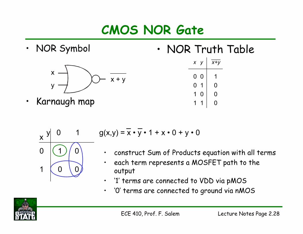
CMOS NOR Gate
• NOR Symbol
• Karnaugh map
x y
0
0
1
1
0
1
0
1
x+y
• NOR Truth Table
x
yx + y 1
0
0
0
y 0 1x
0
1
1 0
0 0
g(x,y) = x • y • 1 + x • 0 + y • 0
• construct Sum of Products equation with all terms
• each term represents a MOSFET path to the output
• ‘1’ terms are connected to VDD via pMOS
• ‘0’ terms are connected to ground via nMOS
Page 29
Lecture Notes Page 2.29ECE 410, Prof. F. Salem
CMOS NOR Gate
• Important Points– series-parallel arrangement
• when nMOS in series, pMOS in parallel, and visa versa
• true for all CMOS logic gates
• allows us to construct more complex logic functions
• CMOS NOR Schematic
• output is LOW if x OR y is true
• parallel nMOS
• output is HIGH when x AND y are false
• series pMOS
g(x,y) = x • y • 1 + x • 0 + y • 0
x
x
y
g(x,y) = x + y
Page 30
Lecture Notes Page 2.30ECE 410, Prof. F. Salem
CMOS NAND Gate• NAND Symbol
• CMOS Schematic
x y
0
0
1
1
0
1
0
1
x•y
• Truth Table
x
yx • y 1
1
1
0
y 0 1x
0
1
1 1
1 0
g(x,y) = (x•y•1) + (x•y•1) + (x•y•1)
(x • y • 0)
• K-map
• output is LOW if x AND y are true
• series nMOS
• output is HIGH when x OR y is false
• parallel pMOS
x
xy
g(x,y) = x y
. .0 .1 .1x y x y= + +
Page 31
Lecture Notes Page 2.31ECE 410, Prof. F. Salem
3-Input Gates
• NOR3
• NAND3
xyz
x+y+zx
y
x y
z
g(x,y) = x+y+z
• Alternate Schematic• what function?
• note shared gate inputs• is input order important?
• in series, parallel, both?
• schematic resembles how the circuit will look in physical layout
xyz
x y z
x y
y
x
z
g(x,y) = x y zx y z
Page 32
Lecture Notes Page 2.32ECE 410, Prof. F. Salem
Review: CMOS NAND/NOR Gates
• NOR Schematic
• output is LOW if x AND y are true
• series nMOS
• output is HIGH when x OR y is false
• parallel pMOS
x
xy
g(x,y) = x y
x
x
y
g(x,y) = x + y
• NAND Schematic
• output is LOW if x OR y is true
• parallel nMOS
• output is HIGH when x AND y are false
• series pMOS
Page 33
Lecture Notes Page 2.33ECE 410, Prof. F. Salem
Complex Combinational Logic
• General logic functions– for example
• How do we construct the CMOS gate?– use DeMorgan principles to modify expression
• construct nMOS and pMOS networks
– use Structured Logic• AOI (AND OR INV)
• OAI (OR AND INV)
f = a • (b + c), f = (d • e) + a • (b + c)
a • b = a + b a + b = a • b
Page 34
Lecture Notes Page 2.34ECE 410, Prof. F. Salem
Using DeMorgan
• DeMorgan Relations– NAND-OR rule
• bubble pushing illustration
• bubbles = inversions
– NOR-AND rule a + b = a • b
x
y
equivalentto
x
y x + yx y
a • b = a + b
x
y
equivalentto
x
yx + y
x y
• pMOS and bubble pushing– Parallel-connected pMOS
• assert-low OR
• creates NAND function
– Series-connected pMOS
• assert-low AND
• creates NOR function
xy
x + yyx
g(x,y) = x + y = x y
x x
y
x y
y
g(x,y) = x y = x + y
to implement pMOS this way, must push all bubbles
to the inputs and remove all NAND/NOR output bubbles
Page 35
Lecture Notes Page 2.35ECE 410, Prof. F. Salem
Rules for Constructing CMOS Gates
• Given a logic function
F = f(a, b, c)
• Reduce (using DeMorgan) to eliminate inverted operations
– inverted variables are OK, but not operations (NAND, NOR)
• Form pMOS network by complementing the inputs
Fp = f(a, b, c)
• Form the nMOS network by complementing the output
Fn = f(a, b, c) = F
• Construct Fn and Fp using AND/OR series/parallel
MOSFET structures
– series = AND, parallel = ORx
xy
g(x,y) = x y
The Mathematical Method
EXAMPLE:
F = ab ⇒
Fp = a b = a+b; OR/parallel
Fn = ab = ab; AND/series
Page 36
Lecture Notes Page 2.36ECE 410, Prof. F. Salem
CMOS Combinational Logic Example
• Construct a CMOS logic gate to implement the function: F = a • (b + c)
• pMOS– Apply DeMorgan expansions
F = a + (b + c)
F = a + ( b • c )
– Invert inputs for pMOSFp = a + (b • c)
– Resulting Schematic
aF
b
c
• nMOS– Invert output for nMOS
Fn = a • (b + c)
– Apply DeMorgannone needed
– Resulting Schematic
a
b c
F=a(b+c)
a
a
b
b
c
c
F=a(b+c)a b
c
F=a(b+c)
14 transistors (cascaded gates)
6 transistors
(CMOS)
Page 37
Lecture Notes Page 2.37ECE 410, Prof. F. Salem
Structured Logic• Recall CMOS is inherently Inverting logic
• Can use structured circuits to implement general logic functions
• AOI: implements logic function in the orderAND, OR, NOT (Invert)
– Example: F = a • b + c • d• operation order: i) a AND b, c AND d, ii) (ab) OR (cd), iii) NOT
– Inverted Sum-of-Products (SOP) form
• OAI: implements logic function in the orderOR, AND, NOT (Invert)
– Example: G = (x+y) • (z+w)• operation order: i) x OR y, z OR w, ii) (x+y) AND (z+w), iii) NOT
– Inverted Product-of-Sums (POS) form
• Use a structured CMOS array to realize such functions
Page 38
Lecture Notes Page 2.38ECE 410, Prof. F. Salem
AOI/OAI nMOS Circuits
• nMOS AOI structure– series txs in parallel
• nMOS OAI structure– series of parallel txs
F = a • b + c • d
XX
error in textbook Figure 2.45
b
e
F = (a +e) • (b +f)
Page 39
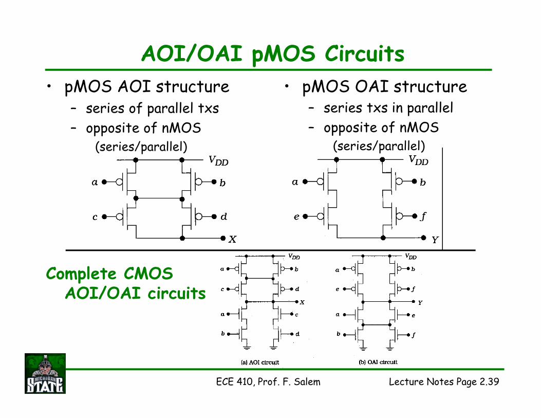
Lecture Notes Page 2.39ECE 410, Prof. F. Salem
AOI/OAI pMOS Circuits
• pMOS AOI structure– series of parallel txs
– opposite of nMOS(series/parallel)
Complete CMOS AOI/OAI circuits
• pMOS OAI structure– series txs in parallel
– opposite of nMOS(series/parallel)
Page 40
Lecture Notes Page 2.40ECE 410, Prof. F. Salem
Implementing Logic in CMOS• Reducing Logic Functions
– fewest operations ⇒ fewest txs– minimized function to eliminate txs– Example: x y + x z + x v = x (y + z + v)
• Suggested approach to implement a CMOS logic function– create nMOS network
• invert output• reduce function, use DeMorgan to eliminate NANDs/NORs• implement using series for AND and parallel for OR
– create pMOS network• complement each operation in nMOS network
– i.e. make parallel into series and visa versa
5 operations:
3 AND, 2 OR
3 operations:
1 AND, 2 OR
# txs = # txs =
Page 41
Lecture Notes Page 2.41ECE 410, Prof. F. Salem
CMOS Logic Example
• Construct the function below in CMOSF = a + b • (c + d); remember AND operations occur before OR
Fn = a + b • (c + d)
• nMOS– Group 2: c & d in parallel
– Group 1: b in series with G2
– Group 3: a parallel to G1/G2
• pMOS– Group 2: c & d in series
– Group 1: b parallel to G2
– Group 3: a in series with G1/G2
• Circuit has an OAOI organization (AOI with extra OR)
Page 42
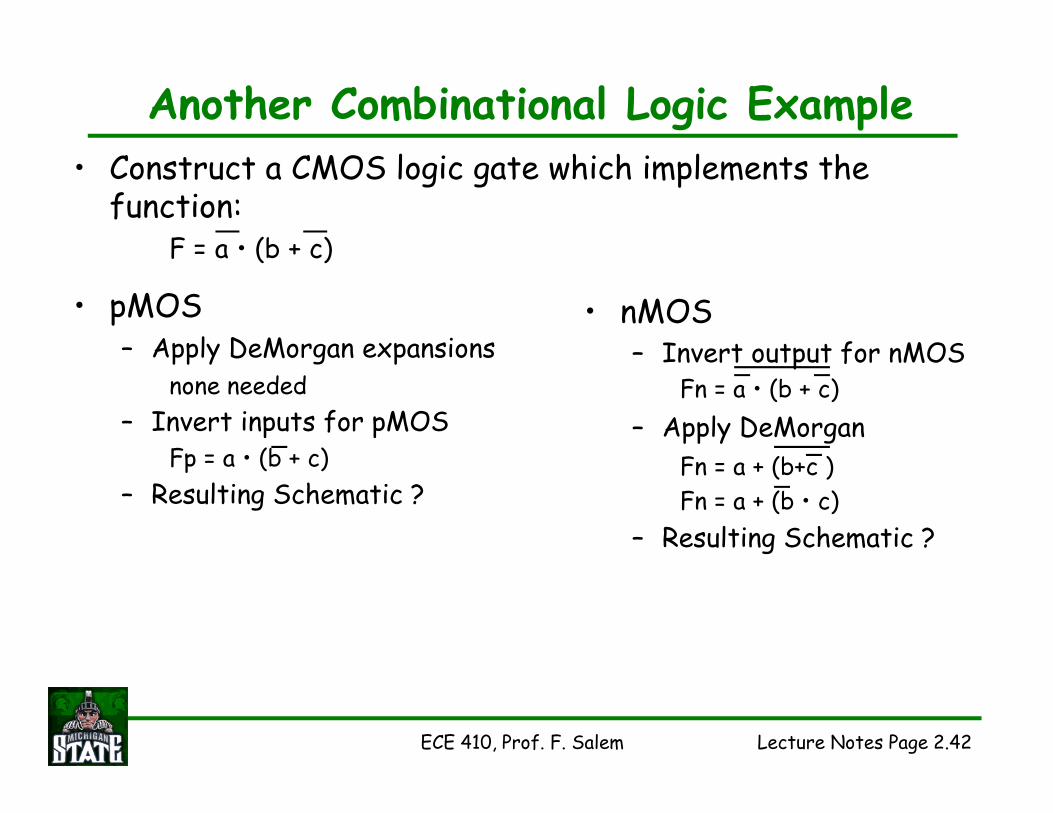
Lecture Notes Page 2.42ECE 410, Prof. F. Salem
Another Combinational Logic Example
• Construct a CMOS logic gate which implements the function:
F = a • (b + c)
• pMOS– Apply DeMorgan expansions
none needed
– Invert inputs for pMOSFp = a • (b + c)
– Resulting Schematic ?
• nMOS– Invert output for nMOS
Fn = a • (b + c)
– Apply DeMorgan
Fn = a + (b+c )
Fn = a + (b • c)
– Resulting Schematic ?
Page 43
Lecture Notes Page 2.43ECE 410, Prof. F. Salem
Yet Another Combinational Logic Example• Implement the function below by constructing the nMOS network
and complementing operations for the pMOS:
F = a • b • (a + c)
• nMOS– Invert Output
• Fn = a • b • (a + c) = a • b + (a + c)
– Eliminate NANDs and NORs
• Fn = a • b + ( a • c)
– Reduce Function
• Fn = a • (b + c)
– Resulting Schematic ?– Complement operations for pMOS
• Fp = a + (b • c)
a
a
b
b
c
c
F=a b (a+c)
Page 44
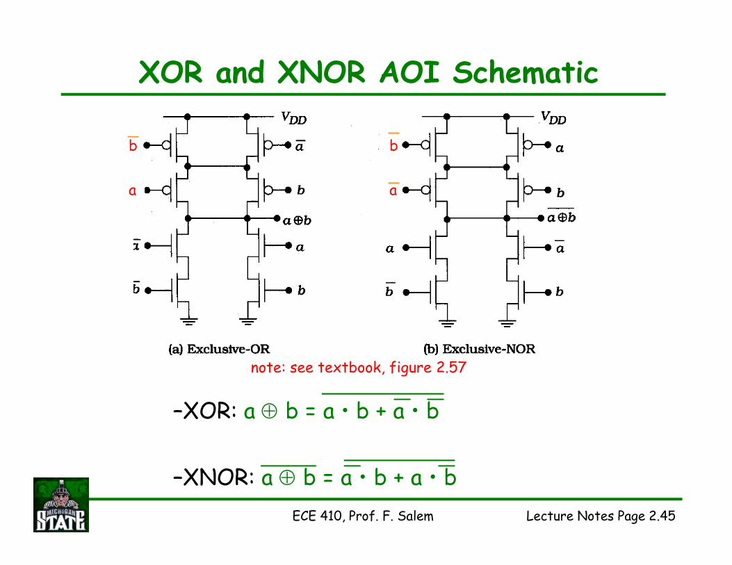
Lecture Notes Page 2.44ECE 410, Prof. F. Salem
XOR and XNOR
• Exclusive-OR (XOR)– a ⊕ b = a • b + a • b
– not AOI form
• Exclusive-NOR– a ⊕ b = a • b + a • b
– inverse of XOR
• XOR/XNOR in AOI form
– XOR: a ⊕ b = a • b + a • b, formed by complementing XNOR above
– XNOR: a ⊕ b = a • b + a • b, formed by complementing XOR
thus, interchanging a and a (or b and b) converts from XOR to XNOR
Page 45
Lecture Notes Page 2.45ECE 410, Prof. F. Salem
XOR and XNOR AOI Schematic
a
–XOR: a ⊕ b = a • b + a • b
–XNOR: a ⊕ b = a • b + a • b
a
b
a
b
note: see textbook, figure 2.57
Page 46
Lecture Notes Page 2.46ECE 410, Prof. F. Salem
CMOS Transmission Gates
• Function– gated switch, capable of passing both ‘1’ and ‘0’
• Formed by a parallel nMOS and pMOS tx
• Controlled by gate select signals, s and s– if s = 1, y = x, switch is closed, txs are on
– if s = 0, y = unknown (high impedance),
switch open, txs off
schematic symbol
recall: pMOS passes a good ‘1’
and nMOS passes a good ‘0’
y = x s, for s=1
Page 47
Lecture Notes Page 2.47ECE 410, Prof. F. Salem
Transmission Gate Logic Functions
• TG circuits used extensively in CMOS– good switch, can pass full range of voltage (VDD-ground)
• 2-to-1 MUX using TGs
F = Po • s + P1 • s
Page 48
Lecture Notes Page 2.48ECE 410, Prof. F. Salem
More TG Functions
• TG XOR and XNOR Gates
• Using TGs instead of
“static CMOS”– TG OR gate
f = a + a b
f = a + b= a b, a = 1
= a, a = 1
a ⊕ b = a • b + a • b
a ⊕ b = a • b + a • b
= a b, b = 1
= a b, b = 1
= a b, b = 1
= a b, b = 1
Page 49
Lecture Notes Page 2.49
Figure 2.64 (p. 59)An XNOR gate that uses both TGs and FETs.
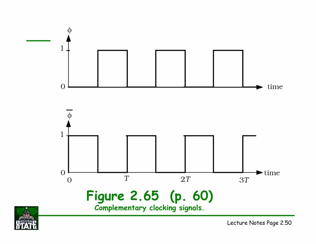
Page 50
Lecture Notes Page 2.50
Figure 2.65 (p. 60)Complementary clocking signals.
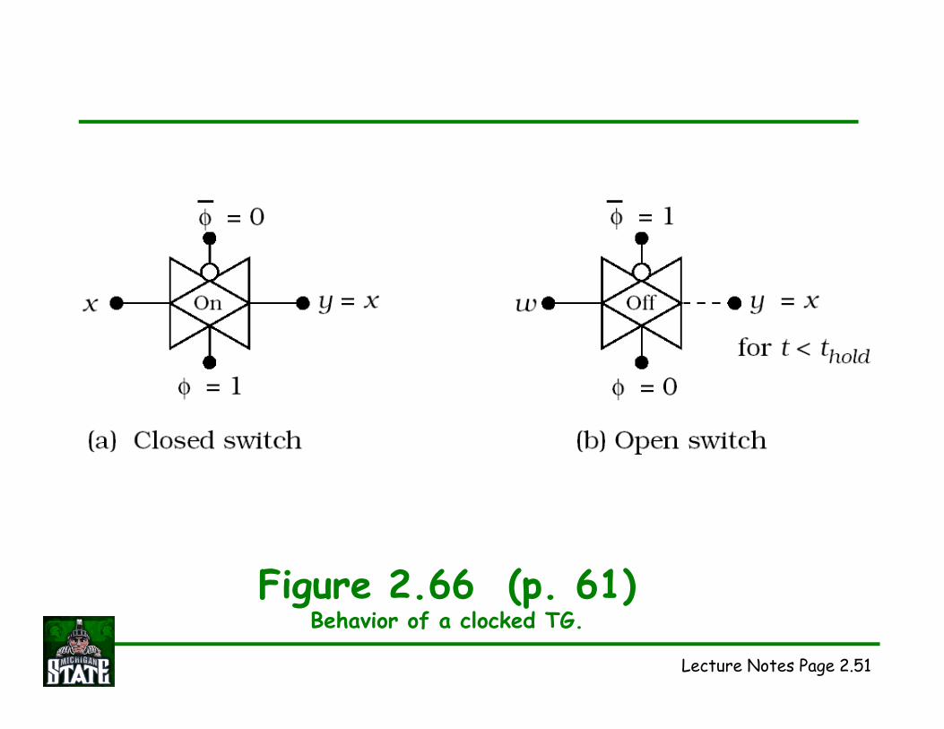
Page 51
Lecture Notes Page 2.51
Figure 2.66 (p. 61)Behavior of a clocked TG.
Page 52
Lecture Notes Page 2.52
Figure 2.67 (p. 61)Data synchronization using transmission gates.
Page 53
Lecture Notes Page 2.53
Figure 2.68 (p. 62)Block-level system timing diagram.
Page 54
Lecture Notes Page 2.54
Figure 2.69 (p. 62)Control of binary words using clocking planes.


![vlsi & embedded systems lab - SIETK ECE DEPARTMENT · 2018. 7. 16. · SIETK, ECE [VLSI & EMBEDDED SYSTEMS LAB] 2 (15A04712) VLSI & EMBEDDED SYSTEMS LABORATORY Note: The students](https://static.documents.pub/doc/80x56/60a68df82b16b22c09239fcb/vlsi-embedded-systems-lab-sietk-ece-department-2018-7-16-sietk-ece.jpg)


![Ece-V-fundamentals of Cmos Vlsi [10ec56]-Notes](https://static.documents.pub/doc/80x56/55cf98ff550346d0339aef5e/ece-v-fundamentals-of-cmos-vlsi-10ec56-notes-562652a532888.jpg)


