Page 1
1Copyright © by Jose E. Schutt-Aine , All Rights ReservedECE 451-Fall 2004
ECE 451Signal Integrity
Fall 2004
Jose E. Schutt-AineElectrical & Computer Engineering
University of [email protected]
Page 2
2Copyright © by Jose E. Schutt-Aine , All Rights ReservedECE 451-Fall 2004
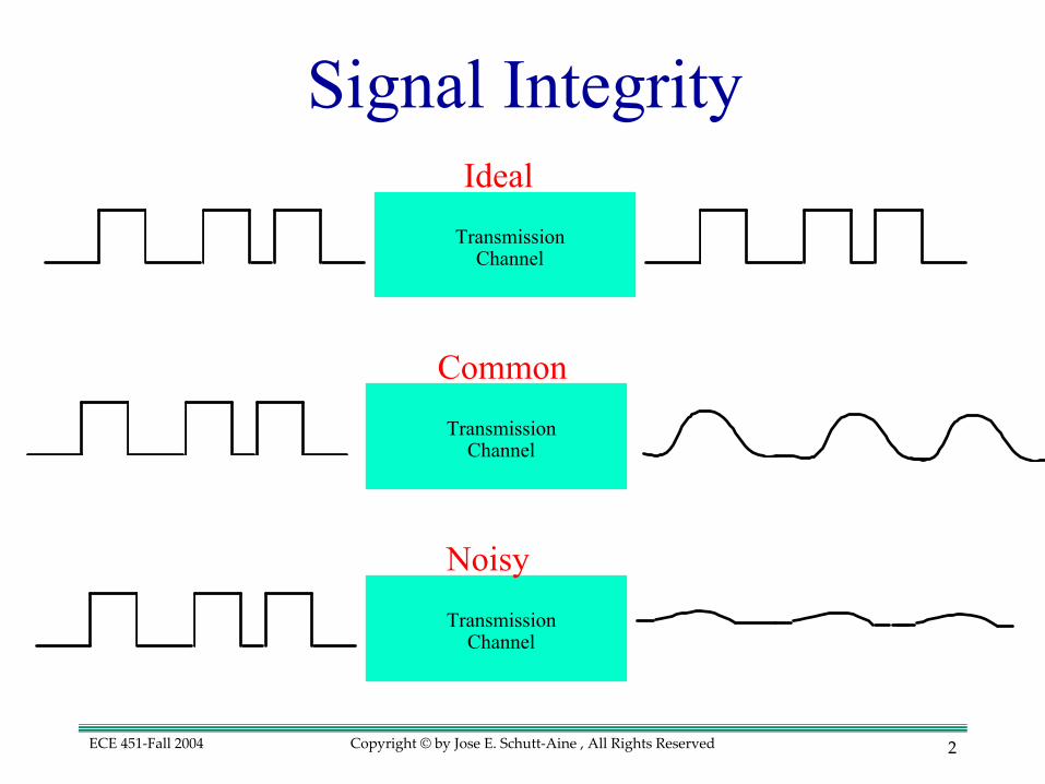
TransmissionChannel
TransmissionChannel
TransmissionChannel
Ideal
Common
Noisy
Signal Integrity
Page 3
3Copyright © by Jose E. Schutt-Aine , All Rights ReservedECE 451-Fall 2004
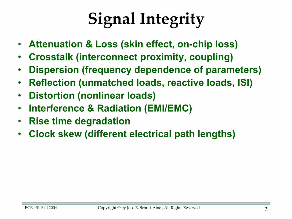
• Attenuation & Loss (skin effect, on-chip loss)• Crosstalk (interconnect proximity, coupling)• Dispersion (frequency dependence of parameters)• Reflection (unmatched loads, reactive loads, ISI)• Distortion (nonlinear loads)• Interference & Radiation (EMI/EMC)• Rise time degradation• Clock skew (different electrical path lengths)
Signal Integrity
Page 4
4Copyright © by Jose E. Schutt-Aine , All Rights ReservedECE 451-Fall 2004
The Interconnect BottleneckThe Interconnect Bottleneck
TechnologyGeneration
MOSFET IntrinsicSwitching Delay
ResponseTime
1.0 um
0.01 um
~ 10 ps
~ 1 ps
~ 1 ps
~ 100 ps
Page 5
5Copyright © by Jose E. Schutt-Aine , All Rights ReservedECE 451-Fall 2004
ChipChip--Level Interconnect DelayLevel Interconnect DelayLine
-0.1
0
0.1
0.2
0.3
0.4
0.5
0.6
0.7
Vol
ts
0 0.4 0.8 1.2 1.6 2Time (ns)
Far End Response
BoardVLSISubmicronDeep Submicron
-0.1
0.175
0.45
0.725
1
0 0.4
Vol
ts
0.8 1.2 1.6 2Time (ns)
Near End Response
BoardVLSISubmicronDeep Submicron
Pulse Characteristics: rise time: 100 ps fall time: 100 ps pulse width: 4ns
Line Characteristics length : 3 mm near end termination: 50 Ω far end termination 65 Ω
LogicthresholdLogic
threshold
Page 6
6Copyright © by Jose E. Schutt-Aine , All Rights ReservedECE 451-Fall 2004
Signal Integrity
Crosstalk Dispersion Attenuation
Reflection Distortion Loss
Delta I Noise Ground Bounce Radiation
Sense Line
Drive Line
Drive Line
Interconnect BottleneckInterconnect Bottleneck
Page 7
7Copyright © by Jose E. Schutt-Aine , All Rights ReservedECE 451-Fall 2004
Reflection in Transmission Lines
1.
2.
3.
Page 8
8Copyright © by Jose E. Schutt-Aine , All Rights ReservedECE 451-Fall 2004
Metallic Conductors
Length
σArea
Re sist an ce : R
Package level:W=3 milsR=0.0045 Ω/mm
R = Le ng thσ Are a
Submicron level:W=0.25 micronsR=422 Ω/mm
Page 9
9Copyright © by Jose E. Schutt-Aine , All Rights ReservedECE 451-Fall 2004
Metal Conductivityσ (Ω-1 m−1 ×10⁻⁷)
Silver 6.1Copper 5.8Gold 3.5Aluminum 1.8Tungsten 1.8Brass 1.5Solder 0.7Lead 0.5Mercury 0.1
Metallic Conductors
Page 10
10Copyright © by Jose E. Schutt-Aine , All Rights ReservedECE 451-Fall 2004
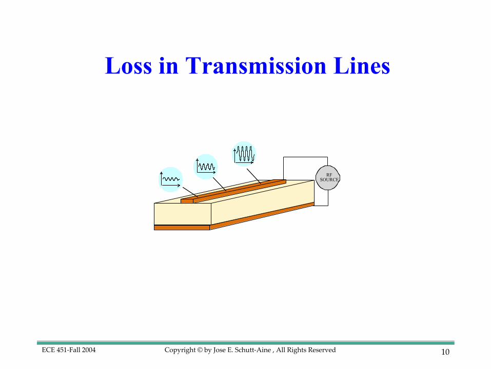
RF SOURCE
Loss in Transmission Lines
Page 11
11Copyright © by Jose E. Schutt-Aine , All Rights ReservedECE 451-Fall 2004
δ
Low Frequency High Frequency Very High Frequency
Skin Effect in Transmission Lines
Page 12
12Copyright © by Jose E. Schutt-Aine , All Rights ReservedECE 451-Fall 2004
. .
Magnitude of current density
y
σ
w
t
e
D
V
J = Joe- y /d e
- jy / d
d
Skin Effect in Microstrip
εr
Page 13
13Copyright © by Jose E. Schutt-Aine , All Rights ReservedECE 451-Fall 2004
The electric field in a material medium propagates as
z
Eoe−γz = Eoe−αze− jβz
where γ = α + jβ. We also have
γ = ω µε(1+jσ
ωε) .
Skin EffectSkin Effect
Wint
δs
δs
Hint
CURRENT AREAS
Page 14
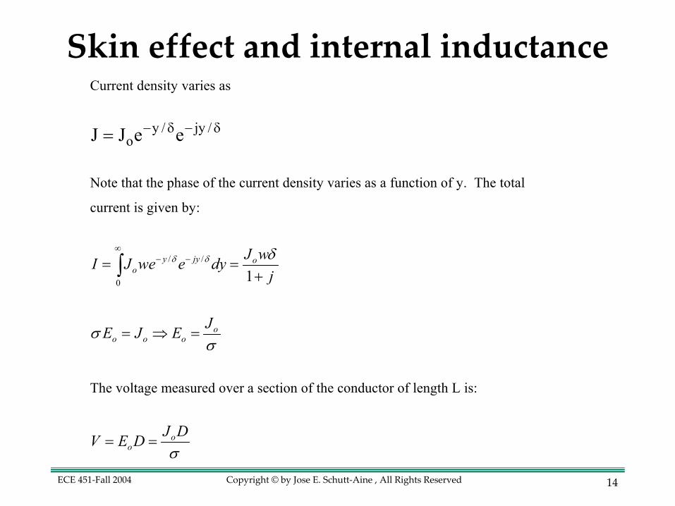
14Copyright © by Jose E. Schutt-Aine , All Rights ReservedECE 451-Fall 2004
Current density varies as
J = Joe−y / δe− jy / δ
Note that the phase of the current density varies as a function of y. The total
current is given by:
/ /
0 1y jy o
oJ wI J we e dy
jδ δ δ∞
− −= =+∫
oo o o
JE J Eσσ
= ⇒ =
The voltage measured over a section of the conductor of length L is:
oo
J DV E Dσ
= =
Skin effect and internal inductance
Page 15
15Copyright © by Jose E. Schutt-Aine , All Rights ReservedECE 451-Fall 2004
The “skin effect” impedance is therefore
(1 ) (1 )oskin
o
J DV j DZ j fI J w w
π µρσ δ
+= = = +
where ρ =1σ
is the bulk resistivity of the conductor
Zskin = Rskin + jXskin
with
skin skinDR X fw
π µρ= =
Skin effect and internal inductance
Page 16
16Copyright © by Jose E. Schutt-Aine , All Rights ReservedECE 451-Fall 2004
−∂V∂z
= (R+ jωL)I = ZI
−∂I∂z
= (G+ jωC)V = YV
Lossy Transmission LineL
∆z
C
I
V
+
-
G
R
Telegraphers Equation
Page 17
17Copyright © by Jose E. Schutt-Aine , All Rights ReservedECE 451-Fall 2004
z
R, L, G, C,
Lossy Transmission Line
forward wave
backward wave
Page 18
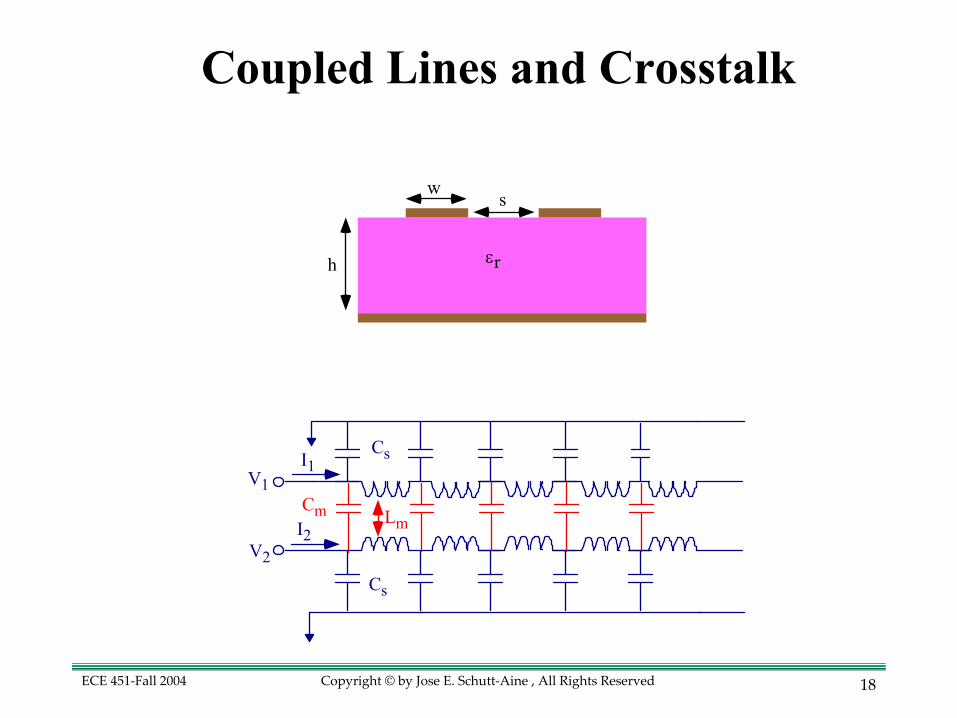
18Copyright © by Jose E. Schutt-Aine , All Rights ReservedECE 451-Fall 2004
Coupled Lines and Crosstalk
εr
w s
h
Cs
V1
V2
I1
I2
Cs
Cm Lm
Page 19
19Copyright © by Jose E. Schutt-Aine , All Rights ReservedECE 451-Fall 2004
50 Ωline 1
line 2
50 Ω
line 1
line 2
50 Ωline 1
line 2
line 1
line 2
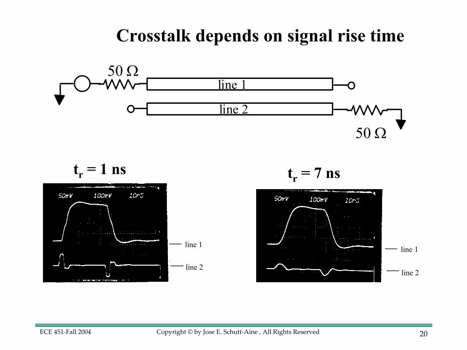
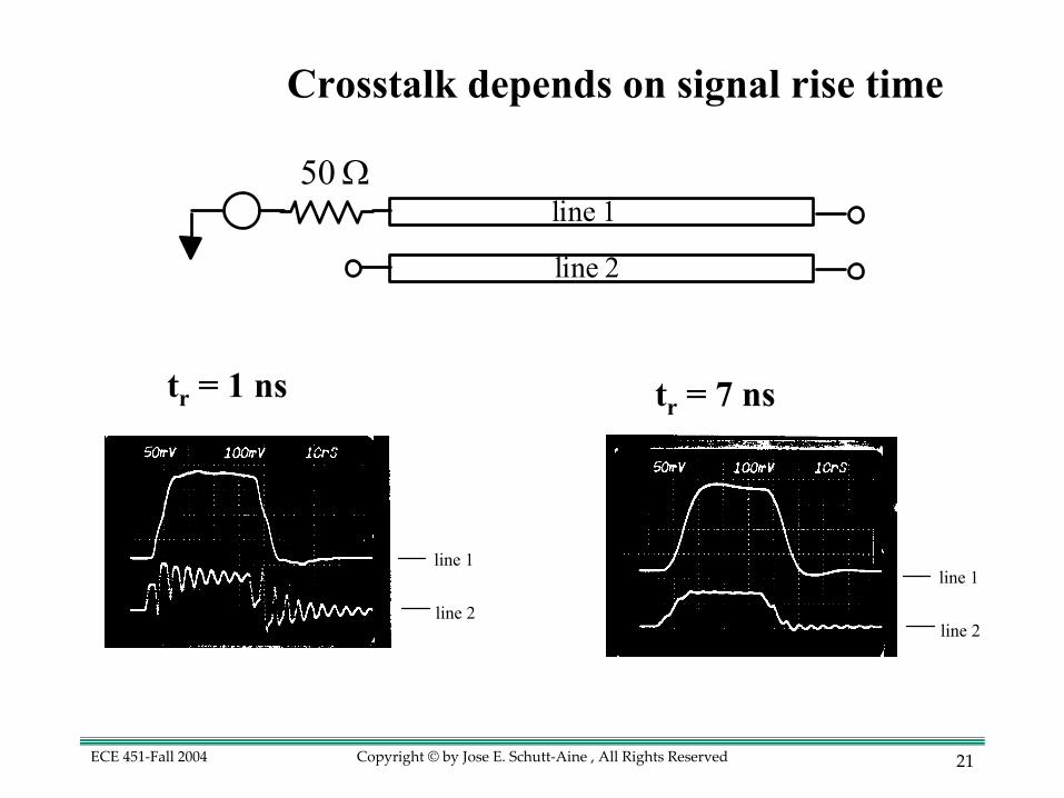
Crosstalk noise depends on termination
Page 20
20Copyright © by Jose E. Schutt-Aine , All Rights ReservedECE 451-Fall 2004
50 Ωline 1
line 2
50 Ω
line 1
line 2
line 1
line 2
tr = 1 ns tr = 7 ns
Crosstalk depends on signal rise time
Page 21
21Copyright © by Jose E. Schutt-Aine , All Rights ReservedECE 451-Fall 2004
tr = 1 ns tr = 7 ns
Crosstalk depends on signal rise time
50 Ωline 1
line 2
line 1
line 2
line 1
line 2
Page 22
22Copyright © by Jose E. Schutt-Aine , All Rights ReservedECE 451-Fall 2004
-0.2
0
0.2
0.4
0.6
0.8
1
Vol
ts
0 5 10 15 20 25 30
Time (ns)
Drive Line at Near End
35 40
-0.15
-0.1
-0.05
0
0.05
0.1
0.15
0.2
Vol
ts
0 5 10 15 20 25 30
Time (ns)
Sense Line at Near End
35 40
Page 23
23Copyright © by Jose E. Schutt-Aine , All Rights ReservedECE 451-Fall 2004
ALS04 ALS240Drive Line 1
Drive Line 2
z=0 z=l
Drive Line 3
Sense Line 4
Drive Line 5
Drive Line 6
Drive Line 7
ALS04
ALS04
ALS04
ALS04
ALS04
ALS240
ALS240
ALS240
ALS240
ALS240
7-Line Coupled-Microstrip System
Ls = 312 nH/m; Cs = 100 pF/m;
Lm = 85 nH/m; Cm = 12 pF/m.
Page 24
24Copyright © by Jose E. Schutt-Aine , All Rights ReservedECE 451-Fall 2004
20010000
1
2
3
4
5Drive line 3 at Near End
Time (ns)2001000
-1
0
1
2
3
4
5Drive Line 3 at Far End
Time (ns)
Drive Line 3
Page 25
25Copyright © by Jose E. Schutt-Aine , All Rights ReservedECE 451-Fall 2004
2001000-1
0
1
2Sense Line at Near End
Time (ns)2001000
-1
0
1
2Sense Line at Far End
Time (ns)
Sense Line
Page 26
26Copyright © by Jose E. Schutt-Aine , All Rights ReservedECE 451-Fall 2004
Multiconductor Simulation
Page 27
27Copyright © by Jose E. Schutt-Aine , All Rights ReservedECE 451-Fall 2004
• Signal launched on a transmission line can be affected by previous signals as result of reflections
• ISI can be a major concern especially if the signal delay is smaller than twice the time of flight
• ISI can have devastating effects
• Noise must be allowed to settled before next signal is sent
Intersymbol Interference (ISI)
Page 28
28Copyright © by Jose E. Schutt-Aine , All Rights ReservedECE 451-Fall 2004
Volts
Time
Waveform beginning transition from low to highwith unsettled noise on the bus
Different starting point due to ISI
Receiver switching threshold
Timing differencedue to ISI
Ideal waveform beginning transistionfrom low to high with no noise on the bus
Intersymbol Interference
Page 29
29Copyright © by Jose E. Schutt-Aine , All Rights ReservedECE 451-Fall 2004
-2
-1
0
1
2
3
4200 MHz switching on above bus
400 MHz switching on above bus
Ideal 400 MHz waveformTime
Probe pointZo = 65 ohms30 ohms
V
Intersymbol Interference and Signal Integrity
Page 30
30Copyright © by Jose E. Schutt-Aine , All Rights ReservedECE 451-Fall 2004
• Minimize reflections on the bus by avoiding impedance discontinuities
• Minimize stub lengths and large parasitics from package sockets or connectors
• Keep interconnects as short as possible (minimize delay)
• Minimize crosstalk effects
Minimizing ISI
Page 31
31Copyright © by Jose E. Schutt-Aine , All Rights ReservedECE 451-Fall 2004
Vih
Vil
Threshold
(waveform into reference load)
(waveform at receiver)
Maximum flight time measuredat last crossing of Vih or Vil
Time
Ringback and Rise Time Control
• Violation into threshold region• Detrimental even if threshold is not crossed• Can exacerbate ISI• Can be aggravated by nonlinear (time varying) terminations • Can increase skew between signals
Page 32
32Copyright © by Jose E. Schutt-Aine , All Rights ReservedECE 451-Fall 2004
• Power supply effects (SSN, ground bounce, rail collapse)• Noise from IC• Receiver transistor mismatches• Return path discontinuities • Coupling to reference voltage circuitry
Voltage Reference Uncertainty
Threshold region
Vref + uncertainty
Vref - uncertainty
Time
Threshold
Vih
Vil
Major Contributors
Page 33
33Copyright © by Jose E. Schutt-Aine , All Rights ReservedECE 451-Fall 2004
Jitter is difference in time of when somethingwas ideally to occur and when it actually did occur.
Some devices specify the amount of marginal jitter and totaljitter that it can take to operate correctly. If the cable addsmore jitter than the receiver’s allowed marginal jitter and total jitter the signal will not be received correctly. In this case the jitter is measured as in the below diagram
Jitter Definition
Page 34
34Copyright © by Jose E. Schutt-Aine , All Rights ReservedECE 451-Fall 2004
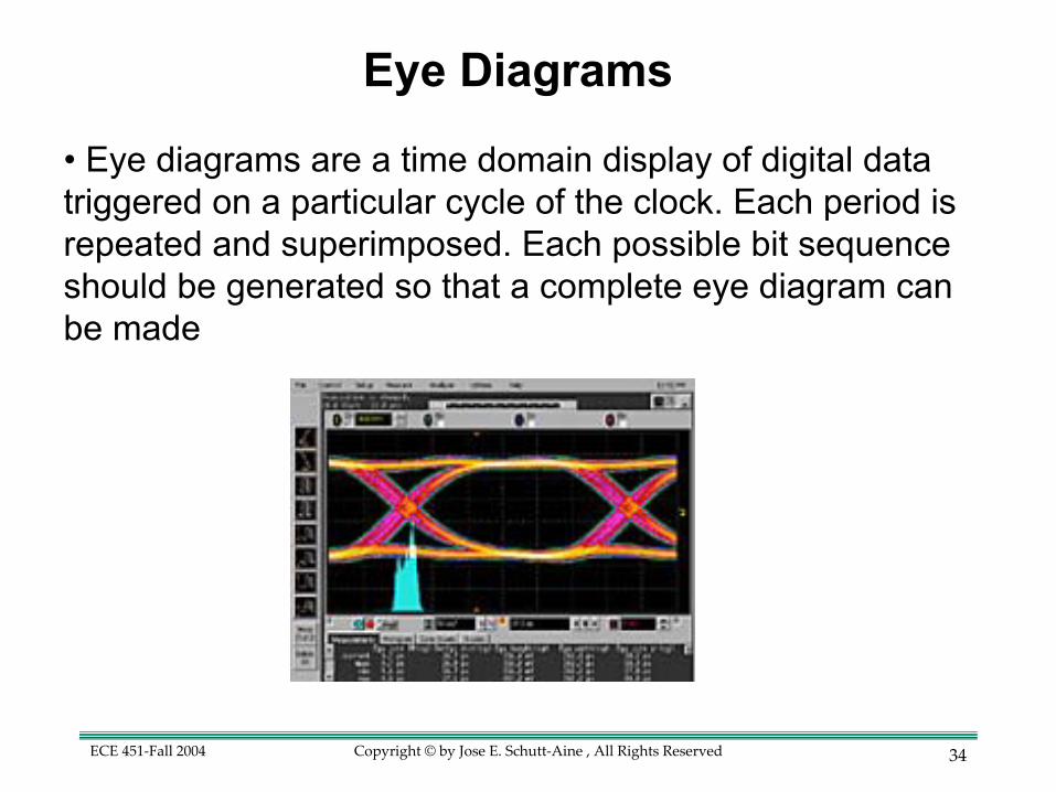
Eye Diagrams
• Eye diagrams are a time domain display of digital data triggered on a particular cycle of the clock. Each period is repeated and superimposed. Each possible bit sequence should be generated so that a complete eye diagram can be made
Page 35
35Copyright © by Jose E. Schutt-Aine , All Rights ReservedECE 451-Fall 2004
Eye Diagram
Page 36
36Copyright © by Jose E. Schutt-Aine , All Rights ReservedECE 451-Fall 2004
Pseudorandomsequencegenerator
Transmitter Receiver
Scope
Trig Vert
Clk
Data
FiberEye Pattern Analysis
Page 37
37Copyright © by Jose E. Schutt-Aine , All Rights ReservedECE 451-Fall 2004
• Jitter is a signal timing deviation referenced to a recovered clock from the recovered bit stream
• Measured in Unit Intervals and captured visually with eye diagrams
• Two types of jitter– Deterministic (non Gaussian)– Random
• The total jitter (TJ) is the sum of the random (RJ) and deterministic jitter(DJ)
Jitter
Page 38
38Copyright © by Jose E. Schutt-Aine , All Rights ReservedECE 451-Fall 2004
• Crosstalk– Noisy neighboring signals
• Interference
• Reflections– Imperfect terminations– Discontinuities (e.g. multidrop buses, stubs)
• Simultaneous switching noise (SSN)– Noisy reference plane or power rail– Shift in threshold voltages
Causes of Deterministic Jitter
Page 39
39Copyright © by Jose E. Schutt-Aine , All Rights ReservedECE 451-Fall 2004
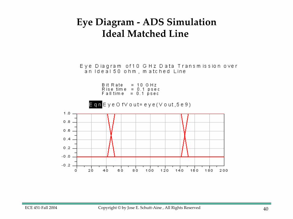
Eye Diagram - ADS Simulation
Page 40
40Copyright © by Jose E. Schutt-Aine , All Rights ReservedECE 451-Fall 2004
Eye Diagram - ADS SimulationIdeal Matched Line
Page 41
41Copyright © by Jose E. Schutt-Aine , All Rights ReservedECE 451-Fall 2004
Eye Diagram - ADS Simulation5 GHz Data Transmission
Page 42
42Copyright © by Jose E. Schutt-Aine , All Rights ReservedECE 451-Fall 2004
Eye Diagram - ADS Simulation5 GHz Data Transmission
Page 43
43Copyright © by Jose E. Schutt-Aine , All Rights ReservedECE 451-Fall 2004
Eye Diagram - ADS Simulation10 GHz Data Transmission
Page 44
44Copyright © by Jose E. Schutt-Aine , All Rights ReservedECE 451-Fall 2004
Eye Diagram - ADS Simulation
Page 45
45Copyright © by Jose E. Schutt-Aine , All Rights ReservedECE 451-Fall 2004
• The Bit-error rate (BER) quantifies the likelihood of a bit being interpreted at the receiver incorrectly due to jitter- or amplitude-induce degradation on the received signal
• No higer than a 10-16 BER is tolerable => no more than 1 error out of 1016 bits.
• BER can be measured directly or quantified with statistical calculations
• Deterministic jitter(DJ) can be easily measured via S-parameters obtained in the frequency domain
Bit-Error Rate