49
ECE 471/571 Timing Issues-II Lecture-14 Gurjeet Singh
ECE 471/571Timing Issues-II
Lecture-14Gurjeet Singh

Synchronizers and Arbiters
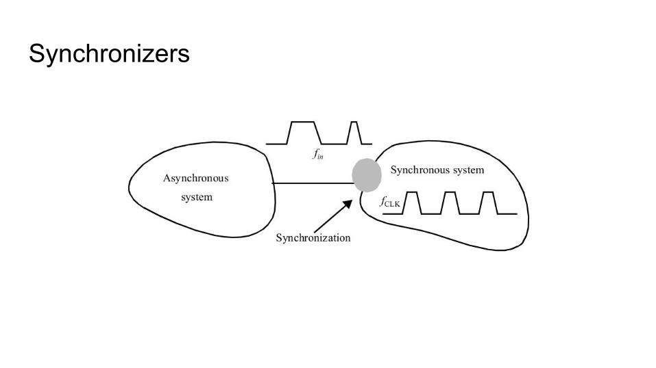
Synchronizers

Simple Synchronizer
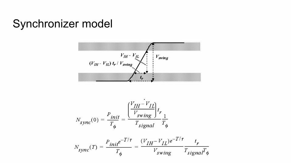
Synchronizer model
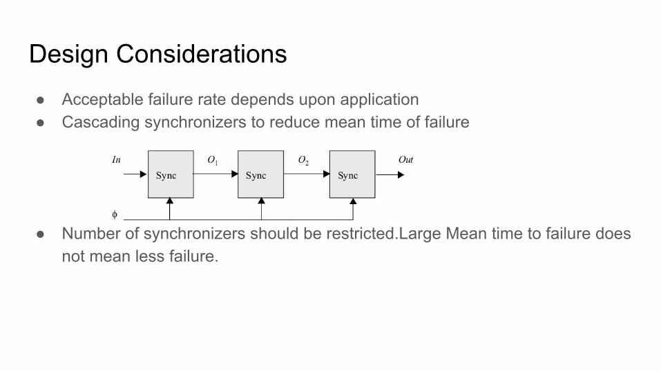
Design Considerations● Acceptable failure rate depends upon application● Cascading synchronizers to reduce mean time of failure
● Number of synchronizers should be restricted.Large Mean time to failure does not mean less failure.
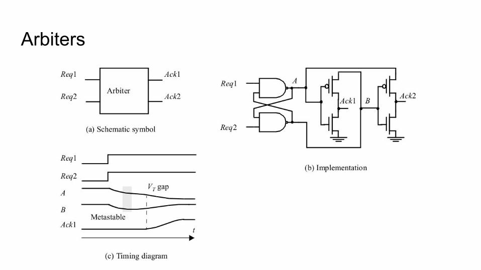
Arbiters
Clock Synthesis and Generation using PLL
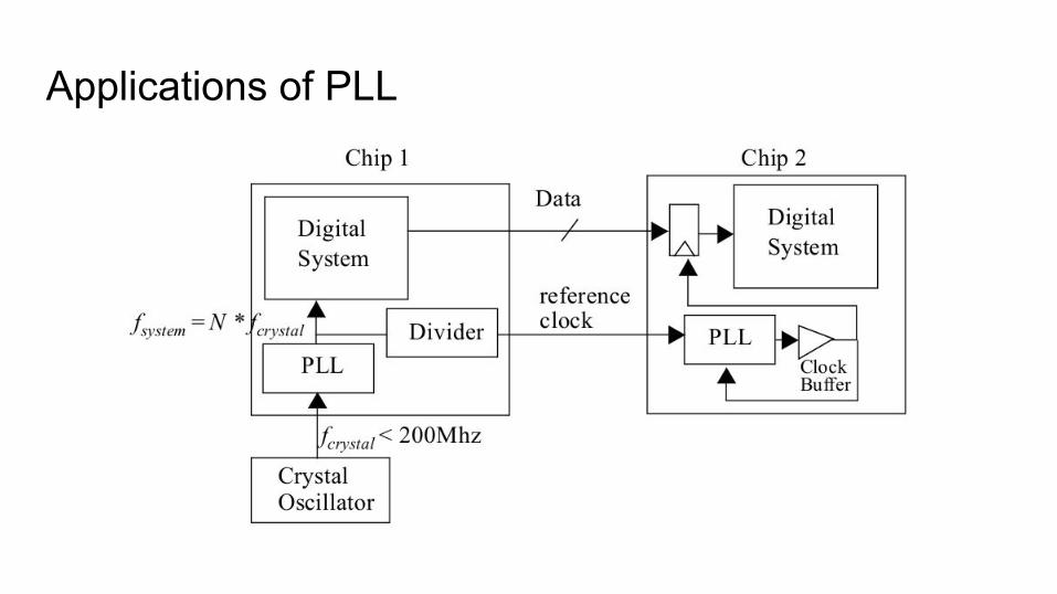
Applications of PLL
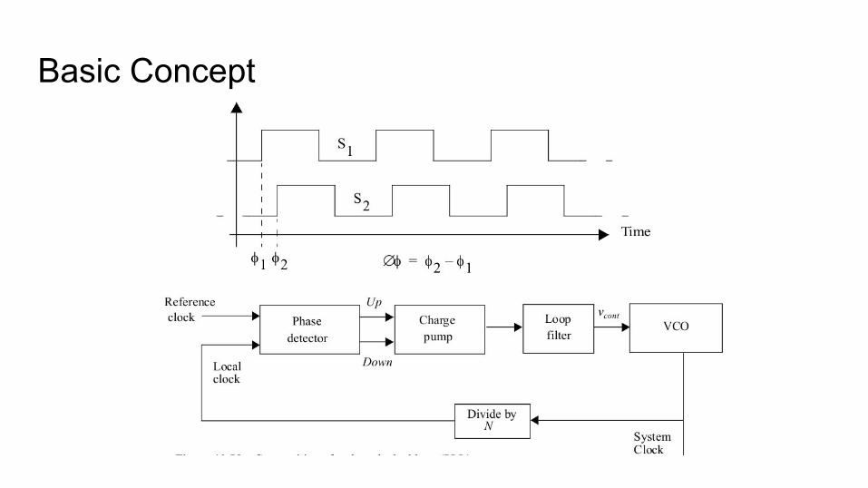
Basic Concept
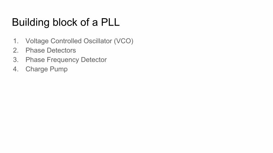
Building block of a PLL1. Voltage Controlled Oscillator (VCO)2. Phase Detectors3. Phase Frequency Detector4. Charge Pump
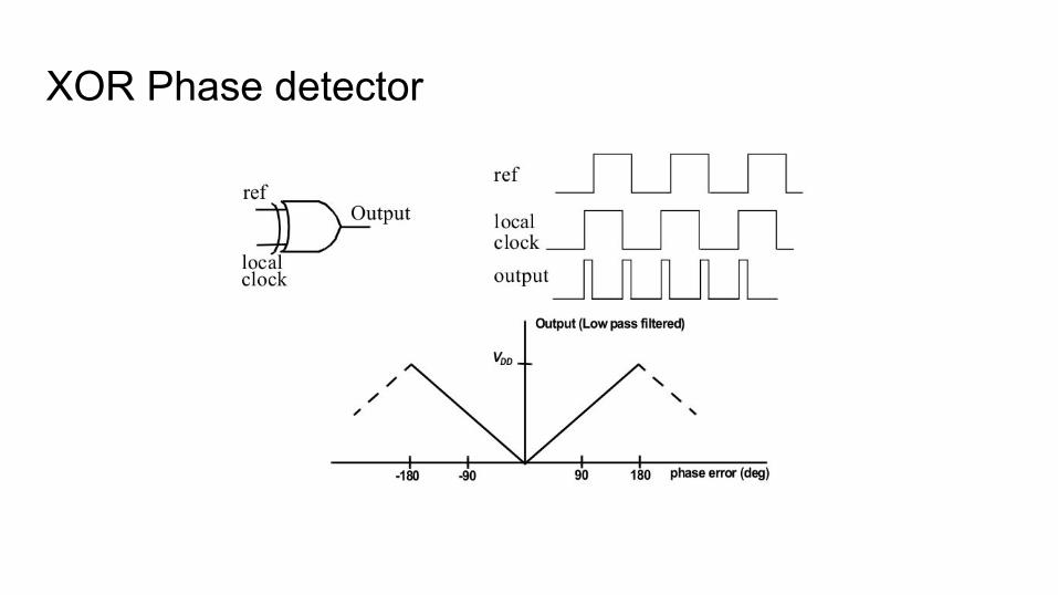
XOR Phase detector
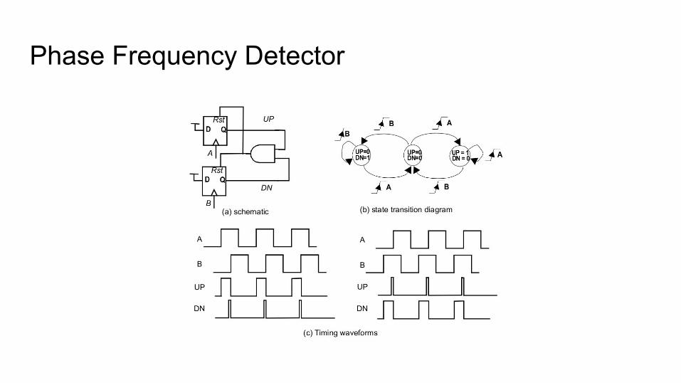
Phase Frequency Detector
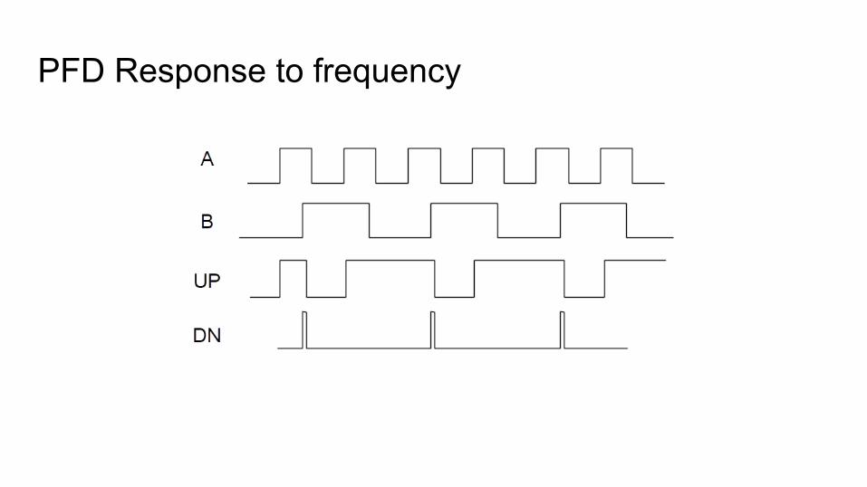
PFD Response to frequency
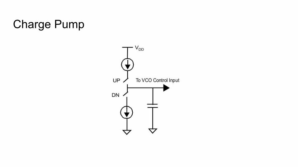
Charge Pump

Future Directions and Perspectives
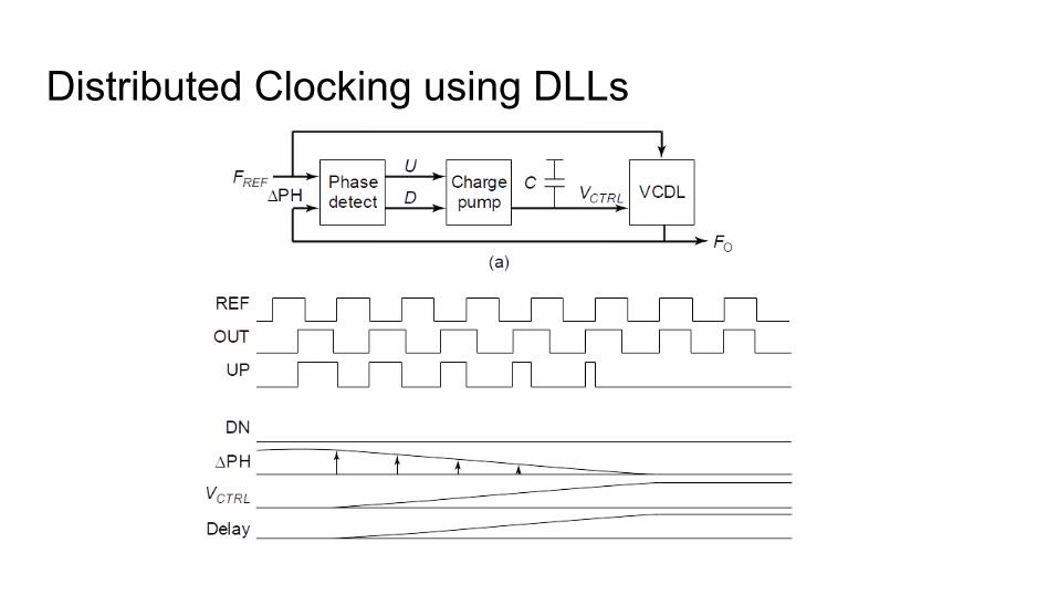
Distributed Clocking using DLLs
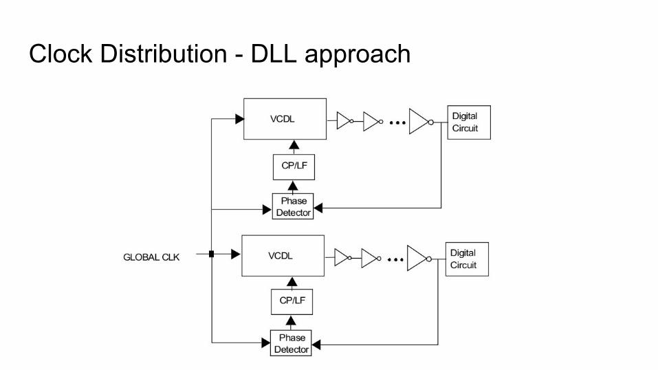
Clock Distribution - DLL approach

Optical Clock Distribution

Summary● Clock skew and Jitter● Self-timed design● Synchronizers● Phase-Locked loops● Delay-Locked loops
Design Arithmetic Building Blocks
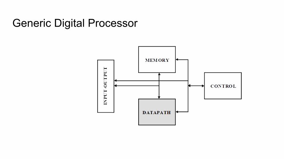
Generic Digital Processor
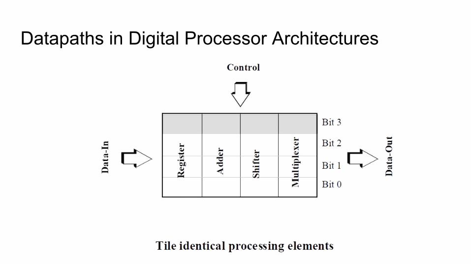
Datapaths in Digital Processor Architectures
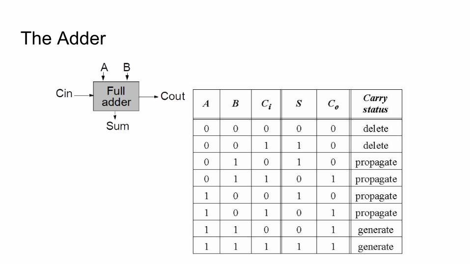
The Adder

The Binary Adder
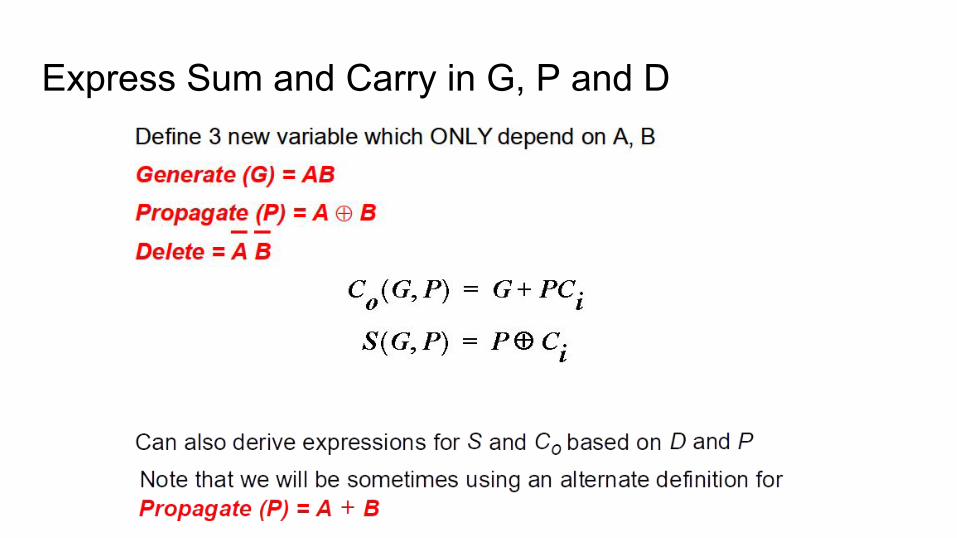
Express Sum and Carry in G, P and D
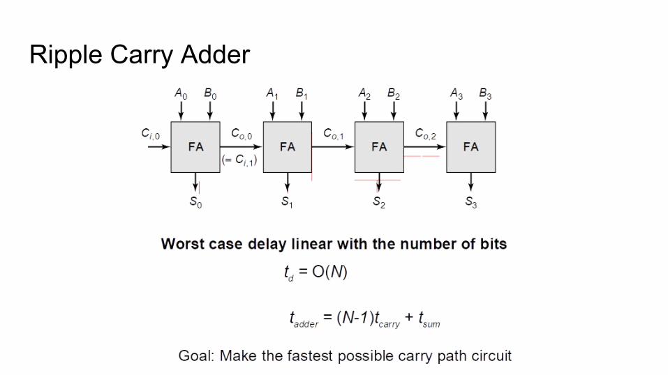
Ripple Carry Adder
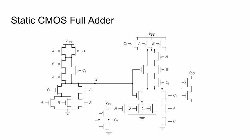
Static CMOS Full Adder
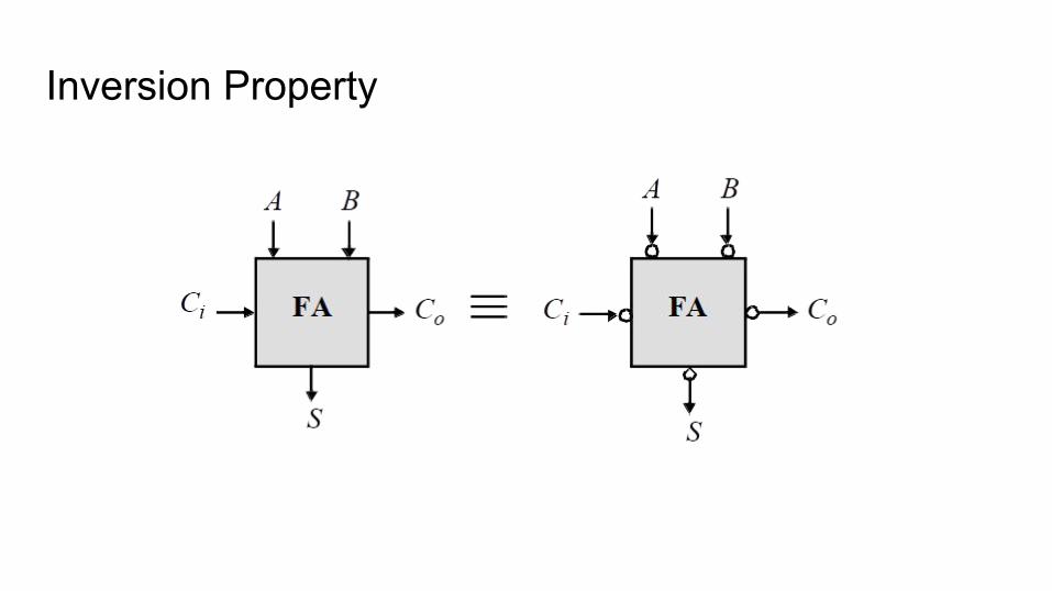
Inversion Property
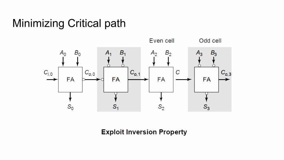
Minimizing Critical path
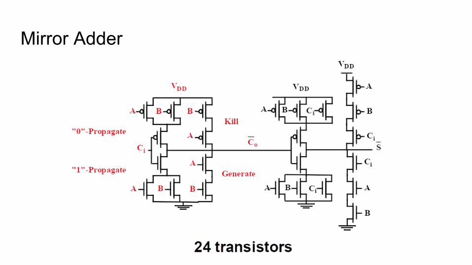
Mirror Adder
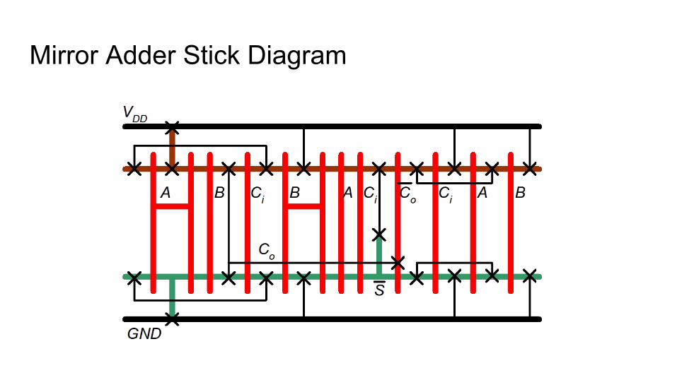
Mirror Adder Stick Diagram

Properties of Mirror Adder● The NMOS and PMOS chains are completely symmetrical.● A maximum of two series transistors can be observed in the carry-generation
circuitry.● When laying out the cell, the most critical issue is the minimization of the
capacitance at node Co. The reduction of the diffusion capacitances is particularly important.
● The capacitance at node Co is composed of four diffusion capacitances, two internal gate capacitances, and six gate capacitances in the connecting adder cell.
● The transistors connected to Ci are placed closest to the output.● Only the transistors in the carry stage have to be optimized for optimal speed. All
transistors in the sum stage can be minimal size.
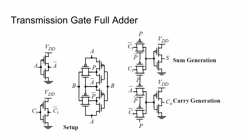
Transmission Gate Full Adder
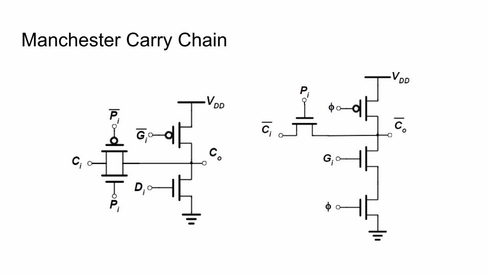
Manchester Carry Chain
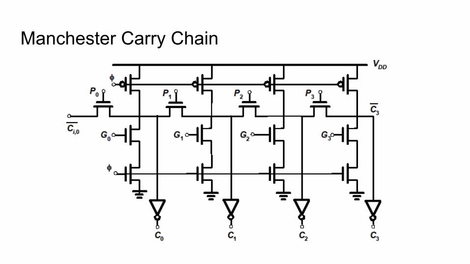
Manchester Carry Chain
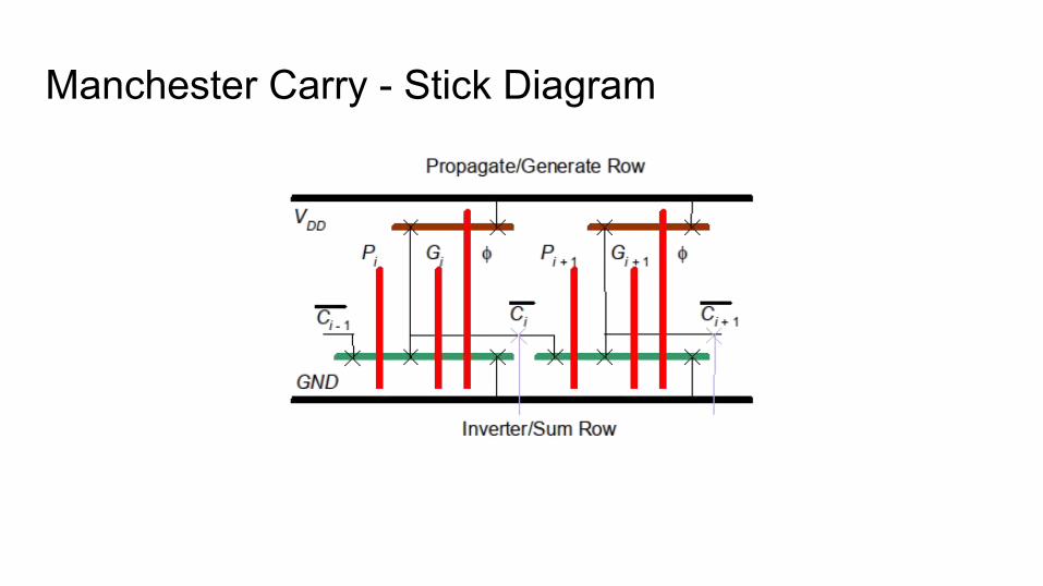
Manchester Carry - Stick Diagram
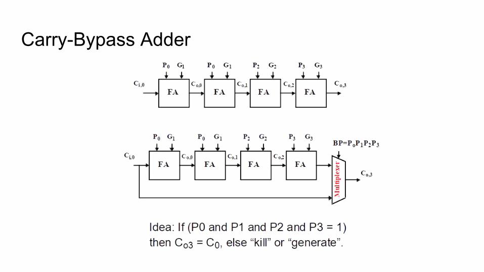
Carry-Bypass Adder
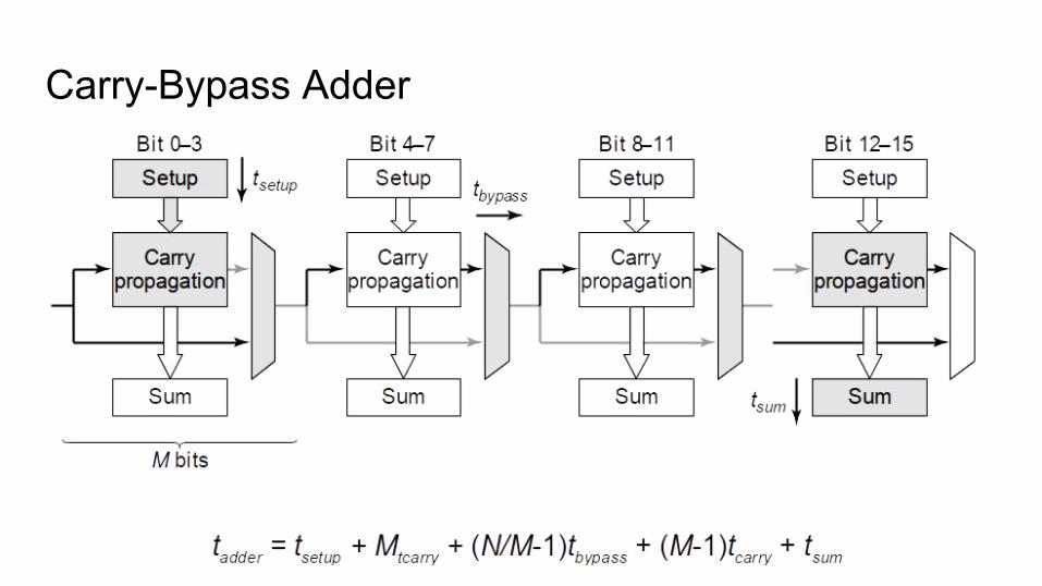
Carry-Bypass Adder
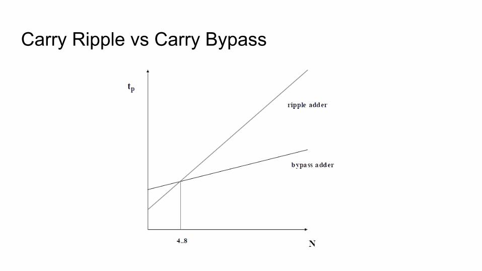
Carry Ripple vs Carry Bypass
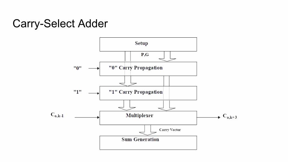
Carry-Select Adder
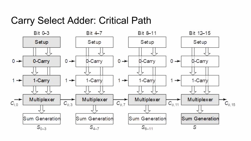
Carry Select Adder: Critical Path
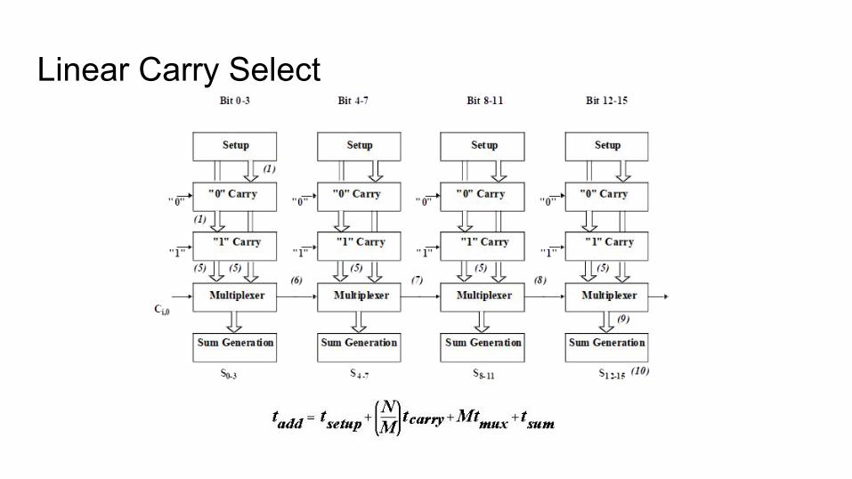
Linear Carry Select
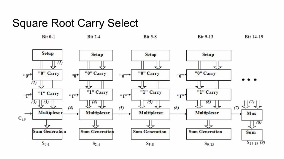
Square Root Carry Select
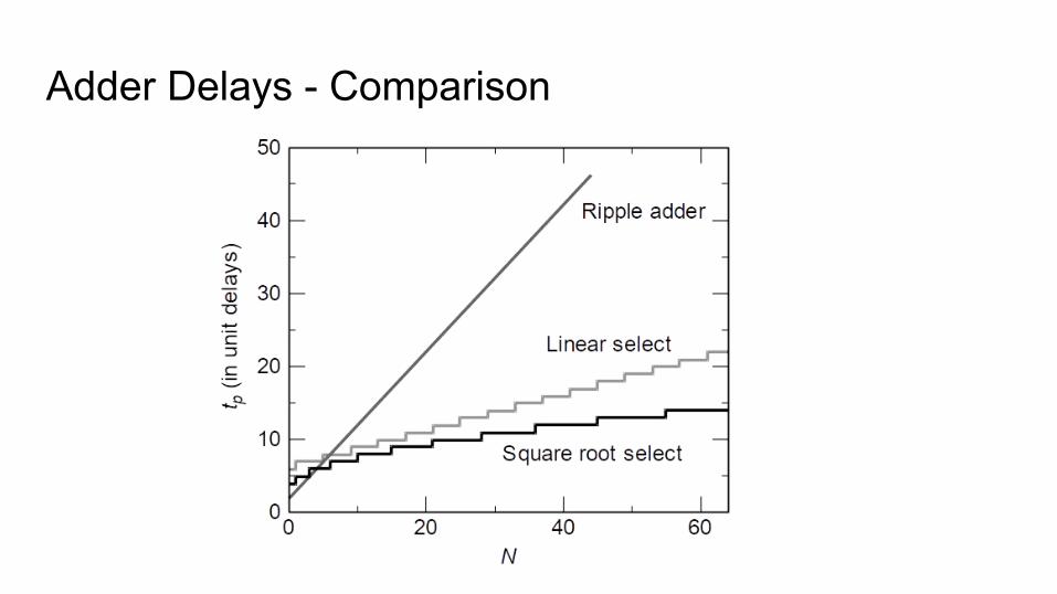
Adder Delays - Comparison
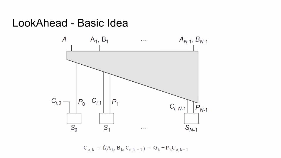
LookAhead - Basic Idea
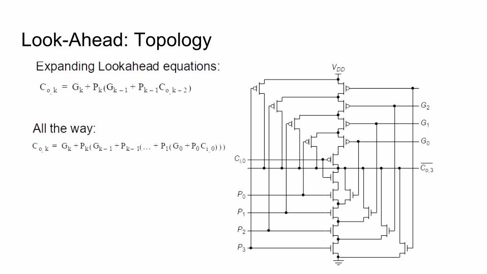
Look-Ahead: Topology
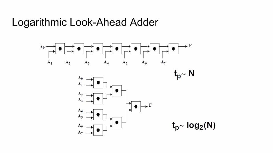
Logarithmic Look-Ahead Adder
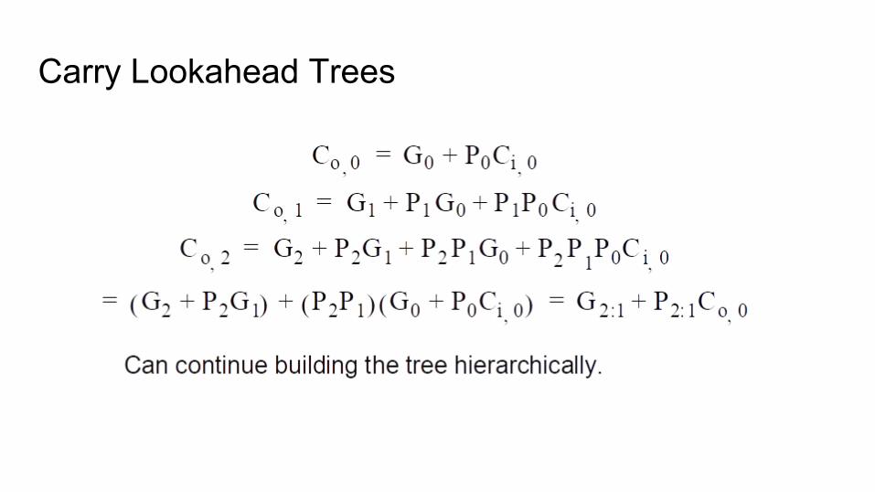
Carry Lookahead Trees


