71
ECE 546 – Jose Schutt‐Aine 1 ECE 546 Lecture ‐20 Power Distribution Networks Spring 2018 Jose E. Schutt-Aine Electrical & Computer Engineering University of Illinois [email protected]
| Date post: | 25-May-2018 |
| Category: |
Documents |
| Upload: | nguyendiep |
| View: | 221 times |
| Download: | 2 times |
ECE 546 – Jose Schutt‐Aine 1
ECE 546Lecture ‐20
Power Distribution NetworksSpring 2018
Jose E. Schutt-AineElectrical & Computer Engineering
University of [email protected]
ECE 546 – Jose Schutt‐Aine 2
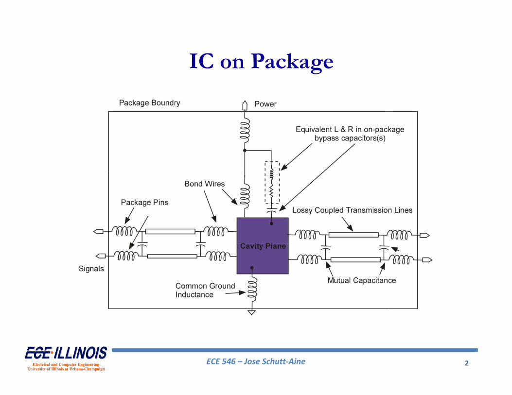
IC on Package
ECE 546 – Jose Schutt‐Aine 3
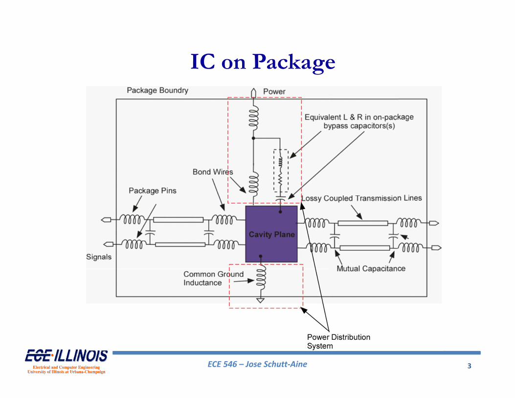
IC on Package
ECE 546 – Jose Schutt‐Aine 44
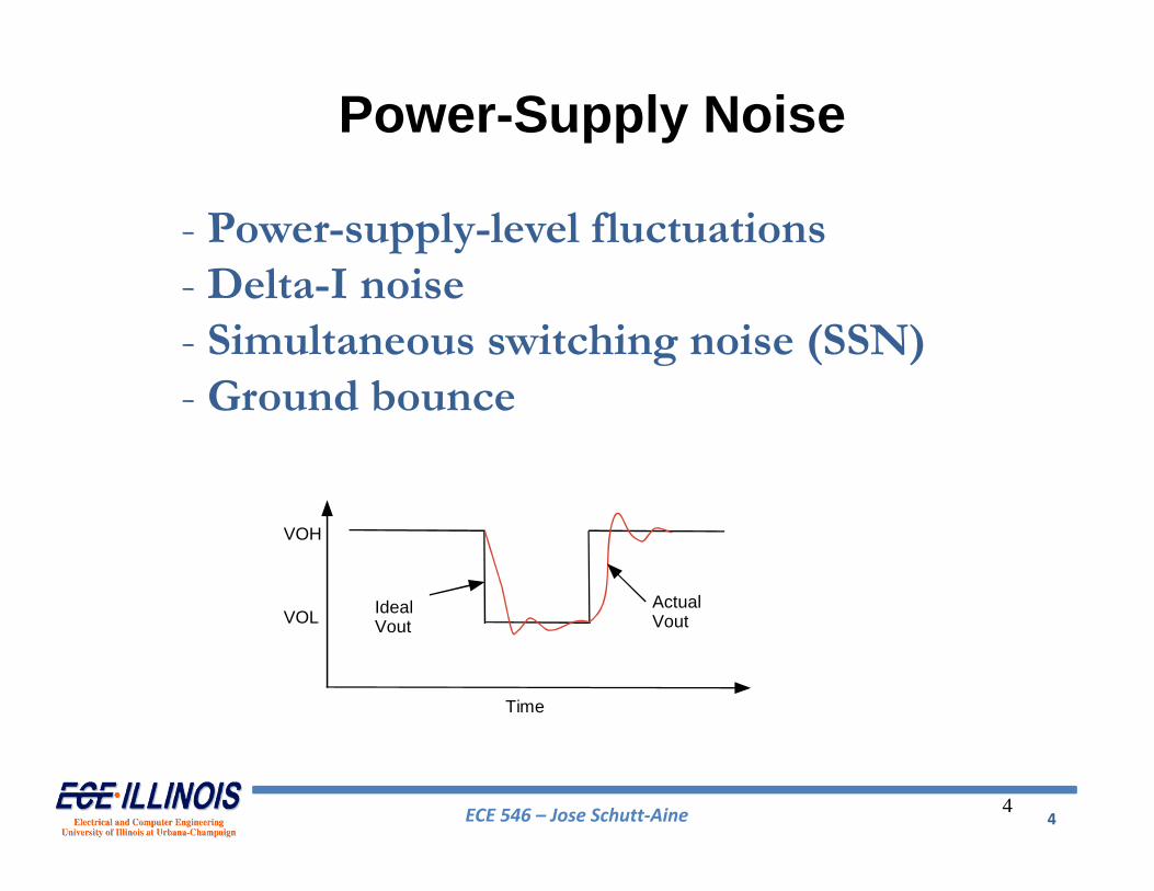
- Power-supply-level fluctuations- Delta-I noise- Simultaneous switching noise (SSN)- Ground bounce
IdealVout
ActualVout
VOH
VOL
Time
Power-Supply Noise
ECE 546 – Jose Schutt‐Aine 5
• Voltage fluctuations can cause the followingReduction in voltage across power supply terminals. May prevent devices from switchingIncrease in voltage across power supply terminalsreliability problemsLeakage of the voltage fluctuation into transistorsTiming errors, power supply noise, delta‐I noise, simultaneous switching noise (SSN)
Voltage Fluctuations
ECE 546 – Jose Schutt‐Aine 6
Power-Supply-Level Fluctuations
• Total capacitive load associated with an IC increases as minimum feature size shrinks
• Average current needed to charge capacitance increases
• Rate of change of current (dI/dt) also increases
• Total chip current may change by large amounts within short periods of time
• Fluctuation at the power supply level due to self inductance in distribution lines
ECE 546 – Jose Schutt‐Aine 7
Reducing Power-Supply-Level Fluctuations
• Decoupling capacitors•Multiple power & ground pins• Taylored driver turn-on characteristics
• Large capacitor charges up during steady state• Assumes role of power supply during current switching• Leads should be small to minimize parasitic inductance• Must be placed as close as possible to the chip
Minimize dI/dt noise
Decoupling capacitors
ECE 546 – Jose Schutt‐Aine 8
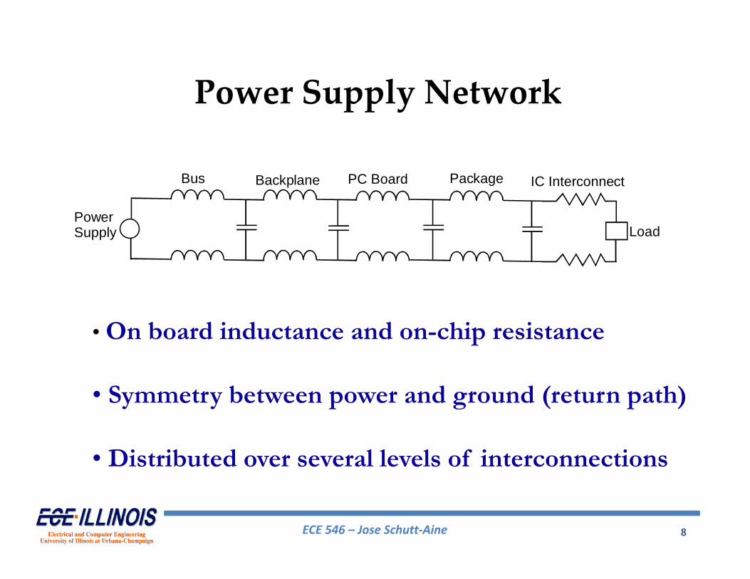
Bus Backplane PC Board Package IC Interconnect
LoadPowerSupply
Power Supply Network
• On board inductance and on-chip resistance
• Symmetry between power and ground (return path)
• Distributed over several levels of interconnections
ECE 546 – Jose Schutt‐Aine 9
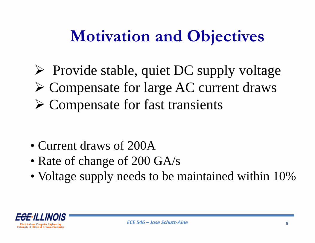
Motivation and Objectives
Provide stable, quiet DC supply voltage Compensate for large AC current draws Compensate for fast transients
• Current draws of 200A• Rate of change of 200 GA/s• Voltage supply needs to be maintained within 10%
ECE 546 – Jose Schutt‐Aine 10
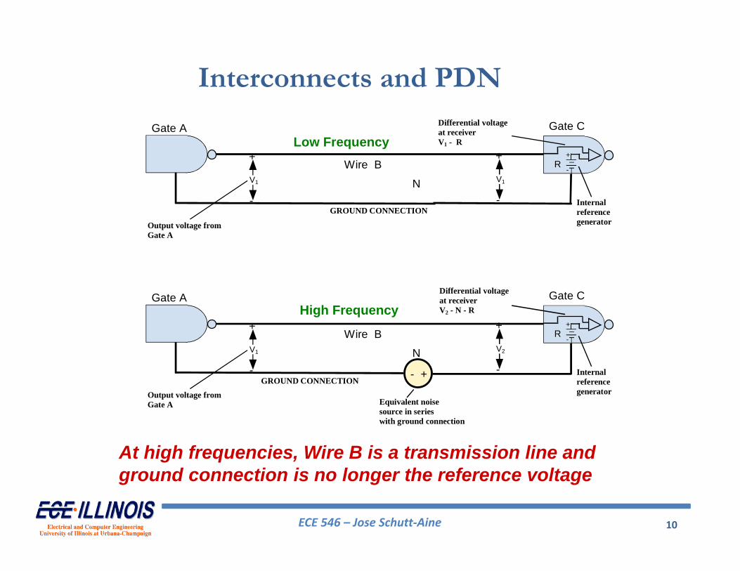
+
-
Gate A Gate C
RWire B
N
Output voltage fromGate A
+
-
V1
Differential voltageat receiverV1 - R
GROUND CONNECTIONInternalreferencegenerator
+
-
V1
+-
+
-
Gate A Gate C
RWire B
N
Equivalent noisesource in serieswith ground connection
Output voltage fromGate A
+
-
V1
Differential voltageat receiverV2 - N - R
GROUND CONNECTIONInternalreferencegenerator
+
-
V2
Interconnects and PDN
At high frequencies, Wire B is a transmission line and ground connection is no longer the reference voltage
Low Frequency
High Frequency
ECE 546 – Jose Schutt‐Aine 11
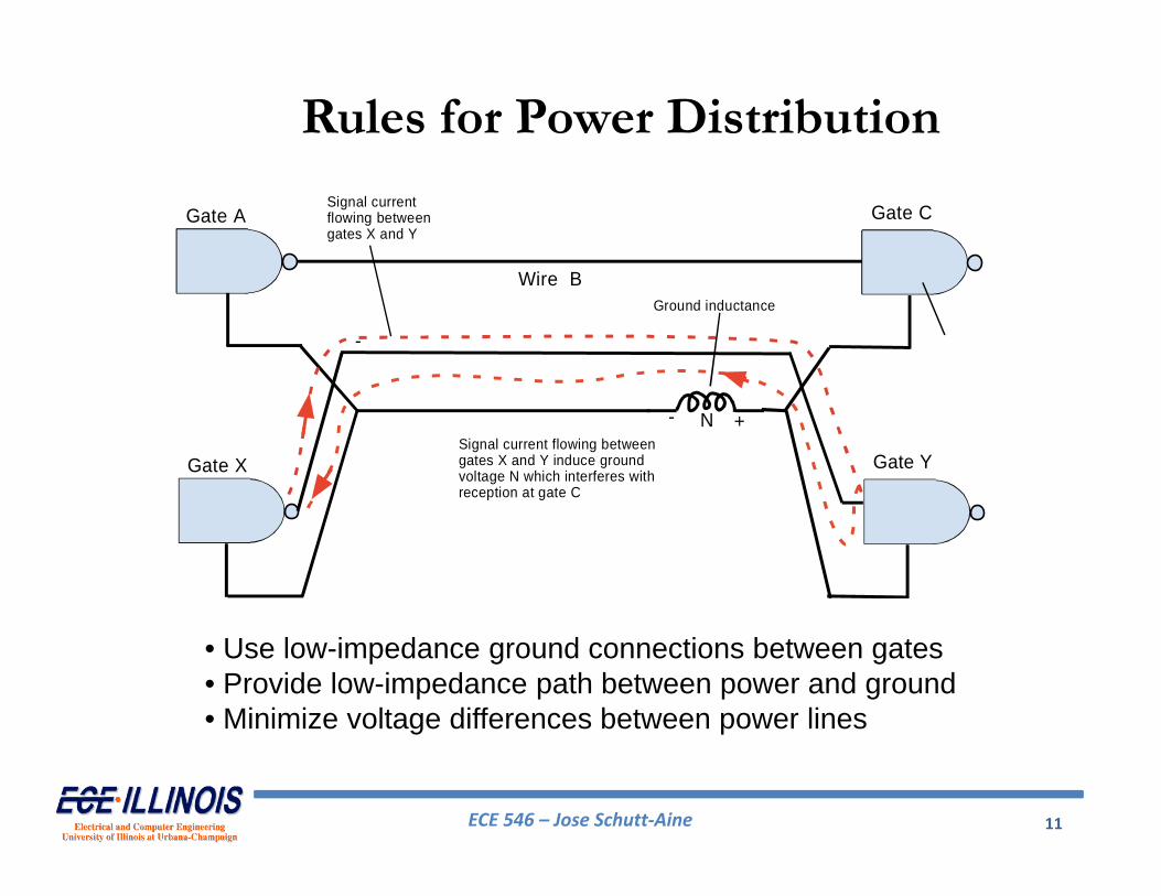
Gate A Gate C
Wire B
N
-
Gate X Gate Y
Signal currentflowing betweengates X and Y
Signal current flowing betweengates X and Y induce groundvoltage N which interferes withreception at gate C
Ground inductance
+-
Rules for Power Distribution
• Use low-impedance ground connections between gates• Provide low-impedance path between power and ground• Minimize voltage differences between power lines
ECE 546 – Jose Schutt‐Aine 12
SSN can affect circuits in 3 ways1) SSN may increase chip-to-chip delays2) Affects the operation of the receiving chips3) May affect gates on the sending chip
Current driven off-chip has only one return path: power and ground pins of the chip carrier to minimize effective inductance of the return path and noise, many power/ground pins must be supplied for off-chip drivers
On-chip circuitry can close the loop by small inductance on chip lines
Effects of SSN
ECE 546 – Jose Schutt‐Aine 13
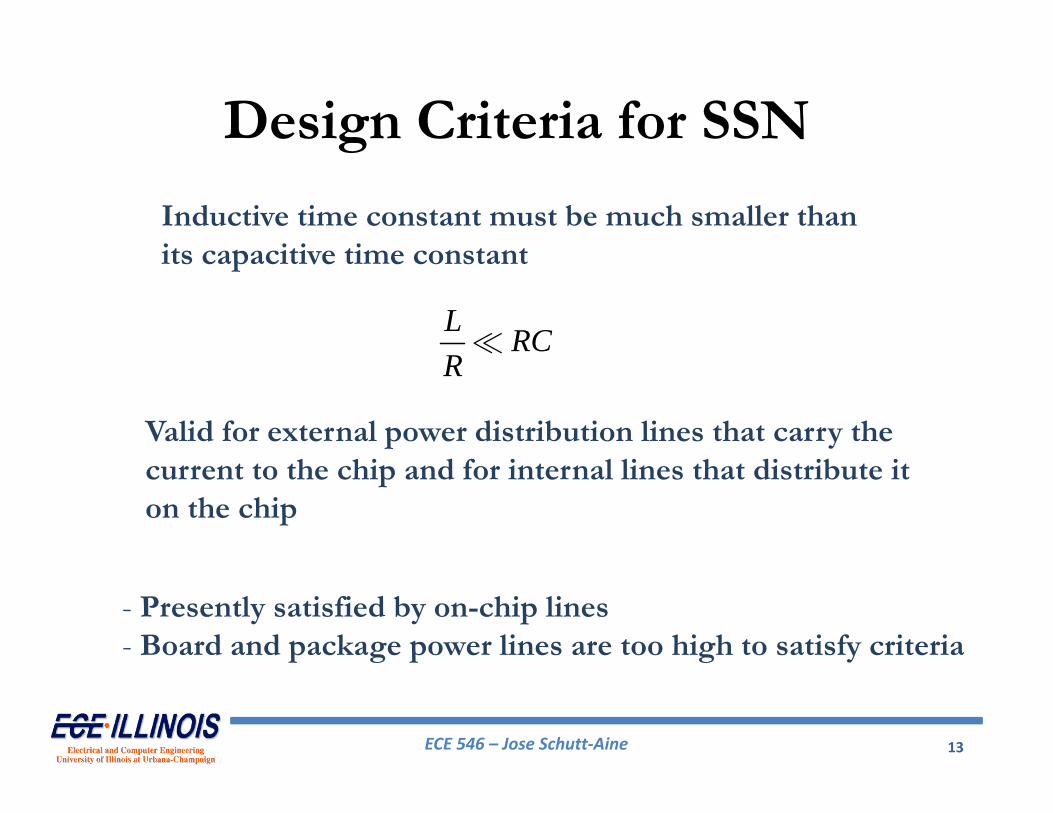
Design Criteria for SSN
Inductive time constant must be much smaller than its capacitive time constant
L RCR
Valid for external power distribution lines that carry the current to the chip and for internal lines that distribute it on the chip
- Presently satisfied by on-chip lines- Board and package power lines are too high to satisfy criteria
ECE 546 – Jose Schutt‐Aine 14
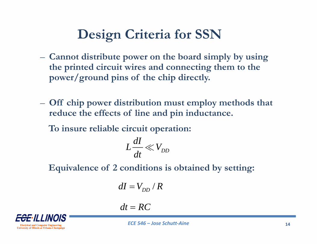
To insure reliable circuit operation:
DDdIL Vdt
Equivalence of 2 conditions is obtained by setting:
/DDdI V R
dt RC
Design Criteria for SSN
– Cannot distribute power on the board simply by using the printed circuit wires and connecting them to the power/ground pins of the chip directly.
– Off chip power distribution must employ methods that reduce the effects of line and pin inductance.
ECE 546 – Jose Schutt‐Aine 15
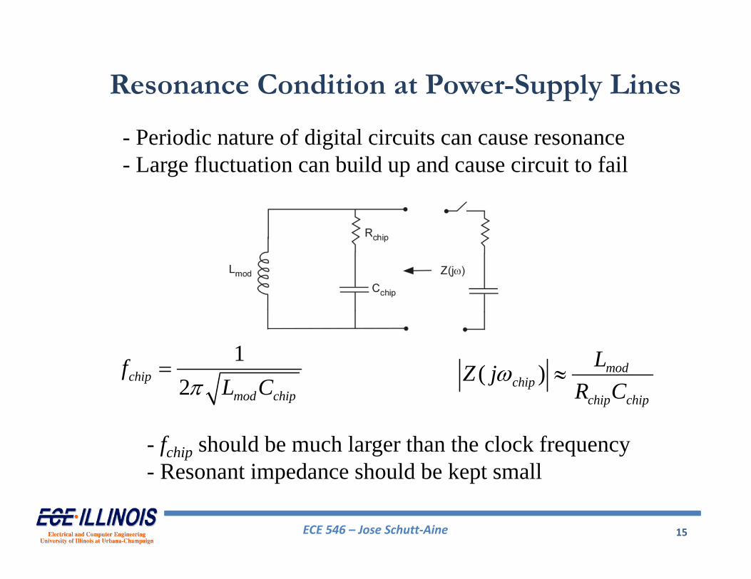
12chip
mod chip
fL C
Resonance Condition at Power-Supply Lines
- Periodic nature of digital circuits can cause resonance- Large fluctuation can build up and cause circuit to fail
( ) modchip
chip chip
LZ jR C
- fchip should be much larger than the clock frequency- Resonant impedance should be kept small
ECE 546 – Jose Schutt‐Aine 16
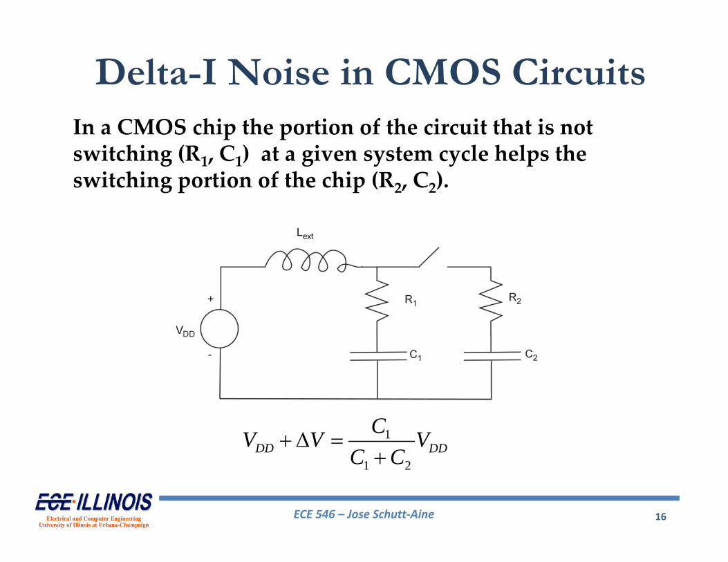
In a CMOS chip the portion of the circuit that is not switching (R1, C1) at a given system cycle helps the switching portion of the chip (R2, C2).
1
1 2DD DD
CV V VC C
Delta-I Noise in CMOS Circuits
ECE 546 – Jose Schutt‐Aine 17
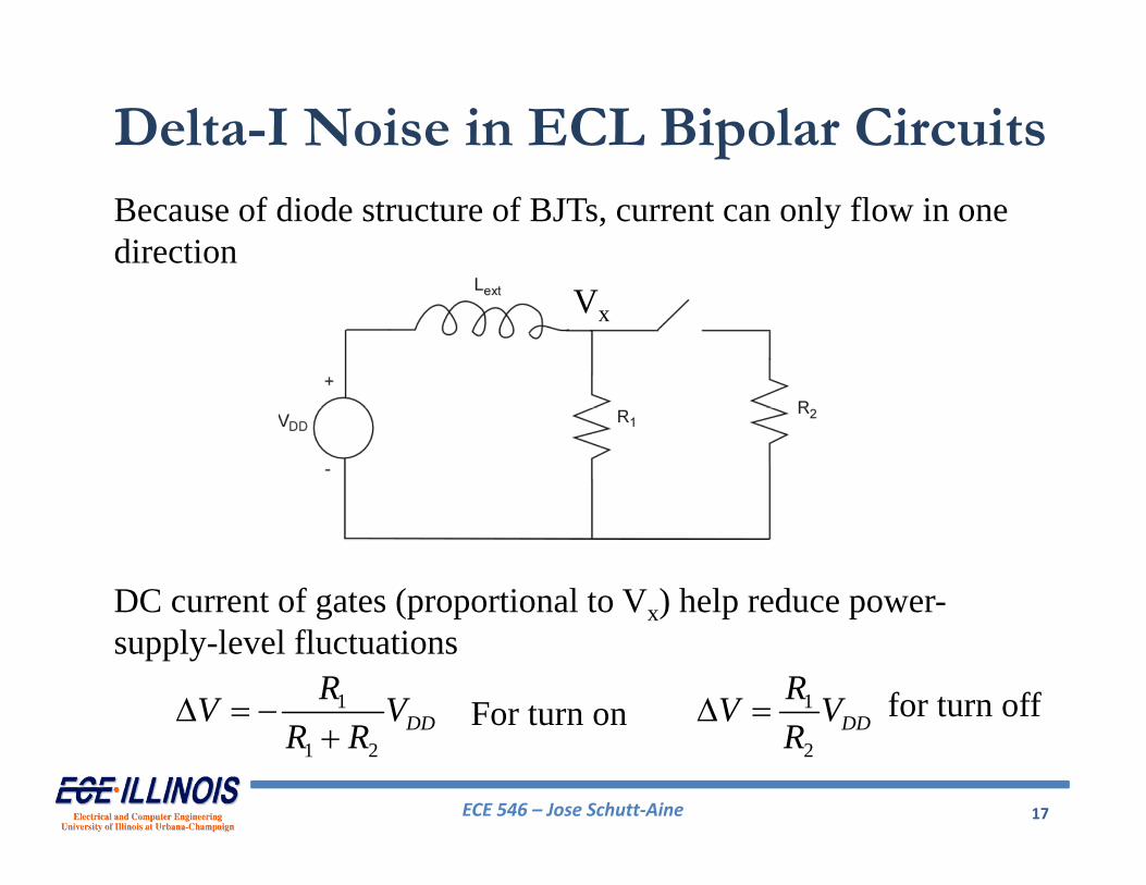
Delta-I Noise in ECL Bipolar CircuitsBecause of diode structure of BJTs, current can only flow in one direction
Vx
DC current of gates (proportional to Vx) help reduce power-supply-level fluctuations
1
1 2DD
RV VR R
1
2DD
RV VR
For turn on for turn off
ECE 546 – Jose Schutt‐Aine 18
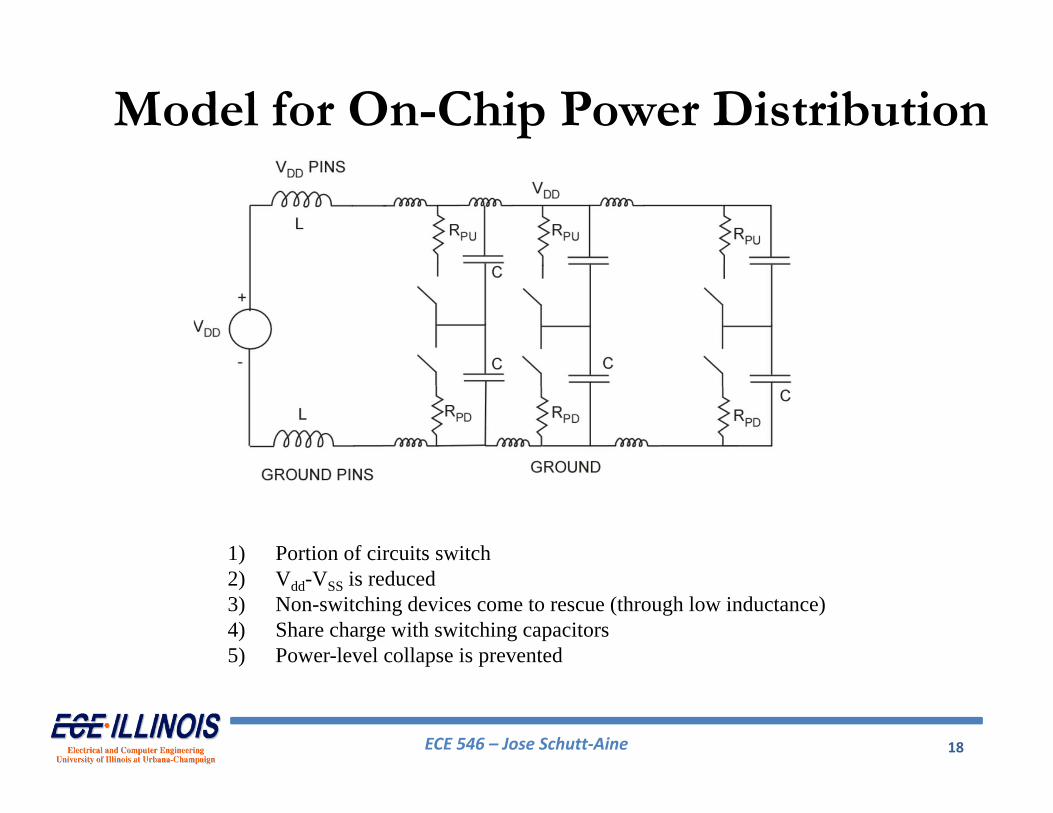
1) Portion of circuits switch2) Vdd-VSS is reduced3) Non-switching devices come to rescue (through low inductance)4) Share charge with switching capacitors5) Power-level collapse is prevented
Model for On-Chip Power Distribution
ECE 546 – Jose Schutt‐Aine 19
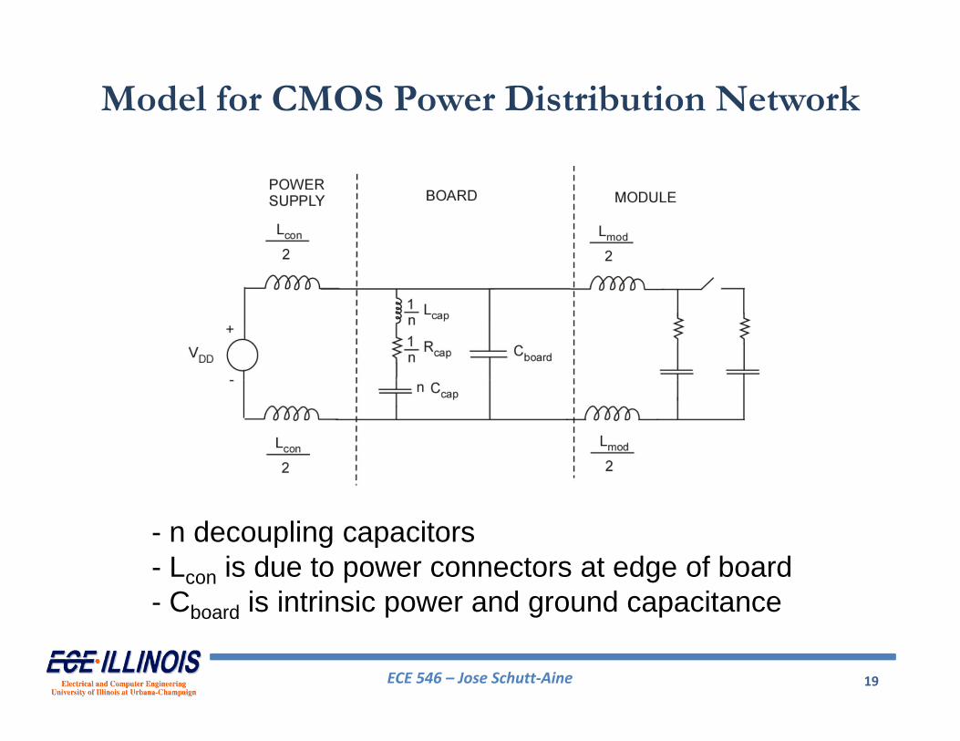
Model for CMOS Power Distribution Network
- n decoupling capacitors- Lcon is due to power connectors at edge of board- Cboard is intrinsic power and ground capacitance
ECE 546 – Jose Schutt‐Aine 20
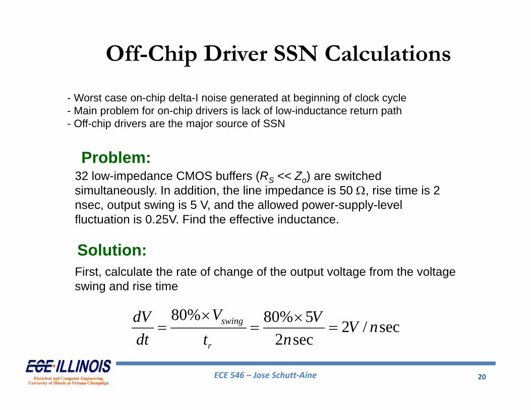
32 low-impedance CMOS buffers (RS << Zo) are switched simultaneously. In addition, the line impedance is 50 , rise time is 2 nsec, output swing is 5 V, and the allowed power-supply-level fluctuation is 0.25V. Find the effective inductance.
Off-Chip Driver SSN Calculations
Problem:
80% 80% 5 2 / sec2 sec
swing
r
VdV V V ndt t n
Solution:First, calculate the rate of change of the output voltage from the voltage swing and rise time
- Worst case on-chip delta-I noise generated at beginning of clock cycle- Main problem for on-chip drivers is lack of low-inductance return path- Off-chip drivers are the major source of SSN
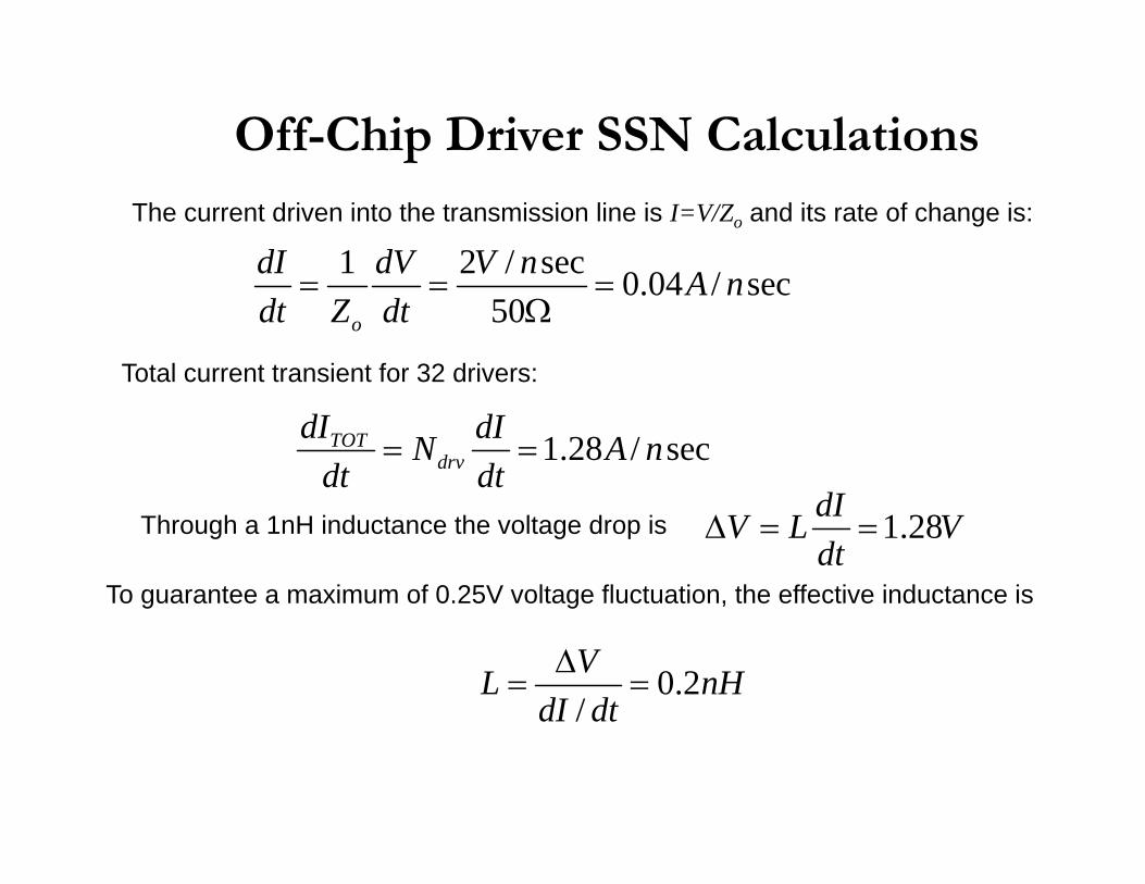
1 2 / sec 0.04 / sec50o
dI dV V n A ndt Z dt
1.28 / secTOTdrv
dI dIN A ndt dt
1.28dIV L Vdt
0.2/VL nH
dI dt
Total current transient for 32 drivers:
Through a 1nH inductance the voltage drop is
To guarantee a maximum of 0.25V voltage fluctuation, the effective inductance is
The current driven into the transmission line is I=V/Zo and its rate of change is:
Off-Chip Driver SSN Calculations
ECE 546 – Jose Schutt‐Aine 22
• A PDN in a system provides the interconnection framework in which gates are allowed to switch states
• Power supplies are bulky and cannot be connected directly to IC, therefore interconnections (with resistance and inductance) are used
• Current through wires create DC drop and voltage fluctuations
• PDN must be created to regulate voltage for required current to be supplied over time
• The speed at which a circuit operates determines the speed at which charge can be supplied or removed from capacitors
PDN Network
ECE 546 – Jose Schutt‐Aine 23
• A PDN consists of a power supply, DC‐DC converters, lots of decoupling capacitors and interconnections
• Power supply provides high voltage and current to motherboard
• Voltage is reduced through a DC‐DC converter•Decoupling capacitors are distributed on the motherboard package and IC and act as charge reservoirs
PDN Network
ECE 546 – Jose Schutt‐Aine 24
• Hierarchy of distribution networks• Usually a tree sometimes a loop• Upper level inductive with distributed caps• On-chip level resistive with distributed caps
General Topology for Power Distribution
ECE 546 – Jose Schutt‐Aine 25
Mechanism• For an IC, the transient current flowing through an inductor gives a voltage drop V=LdI/dt
• Positive dI/dt leads to reduction in supply voltage. Negative dI/dt results into an increase in supply voltage reliability problems has several components
• Supply noise has several componentsUltra high frequency noise ~ 100 GHzHigh‐frequency noise 100 MHz‐1GHzMid‐frequency noise 1‐10 MHzLow frequency noise 1‐100 KHz
ECE 546 – Jose Schutt‐Aine 26
IC PDN
• Core: Primarily made of transistors• I/O: Provides communication with other ICs• Core and I/O require separate PDN
•Goal: ensure sufficient charge is supplied to switching CKT so capacitance can be charged to required voltage
• Charge has to be supplied within a short timeminimize delay need L/R<<RC
ECE 546 – Jose Schutt‐Aine 27
• Used to prevent overshoot so voltage cannot exceed nominal value by more than a small amount.
• Supply overshoot can be reduced via clamping
• Supply voltage droops can be reduced using shunt regulators
• Clamps draw little power and are inexpensive
• Shunt regulators dissipate considerable average power and are expensive
Local Regulation
ECE 546 – Jose Schutt‐Aine 28
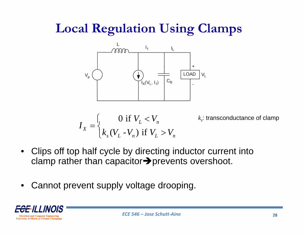
Local Regulation Using Clamps
0 if ( - ) if
L nX
s L n L n
V VI
k V V V V
• Clips off top half cycle by directing inductor current into clamp rather than capacitorprevents overshoot.
• Cannot prevent supply voltage drooping.
ks: transconductance of clamp
ECE 546 – Jose Schutt‐Aine 29
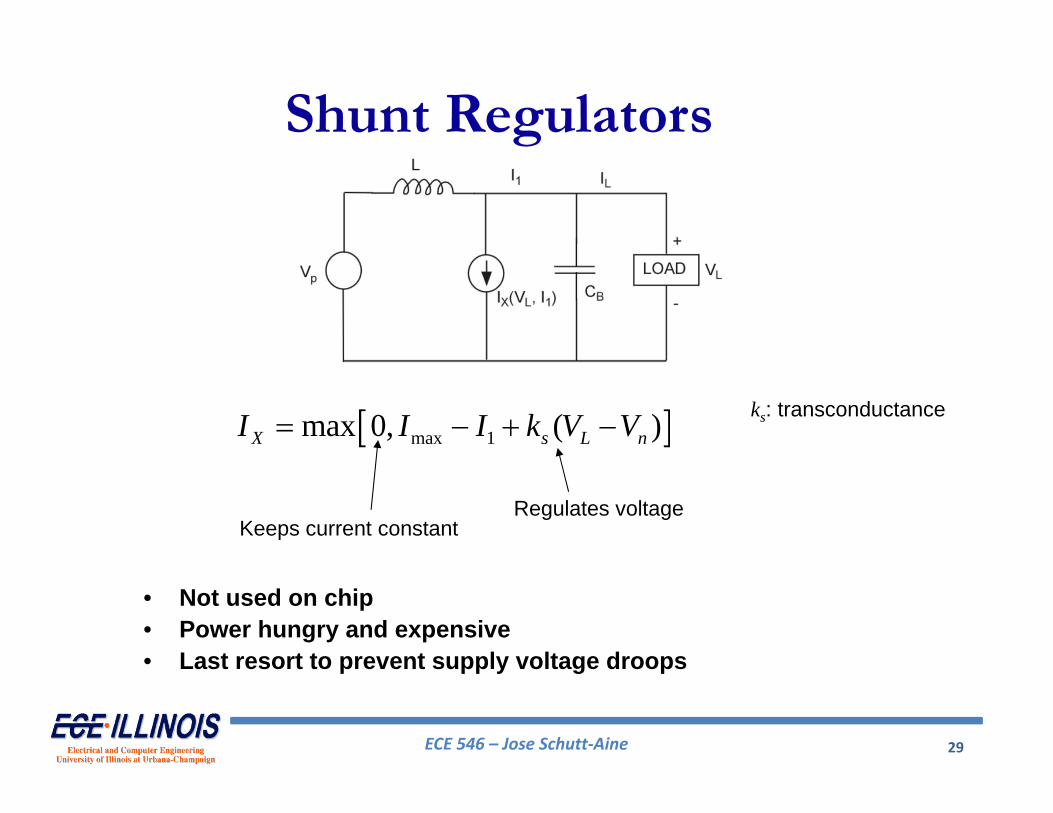
Shunt Regulators
ks: transconductance max 1max 0, ( )X s L nI I I k V V
Keeps current constantRegulates voltage
• Not used on chip• Power hungry and expensive• Last resort to prevent supply voltage droops
ECE 546 – Jose Schutt‐Aine 30
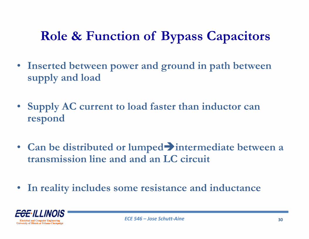
• Inserted between power and ground in path between supply and load
• Supply AC current to load faster than inductor can respond
• Can be distributed or lumpedintermediate between a transmission line and and an LC circuit
• In reality includes some resistance and inductance
Role & Function of Bypass Capacitors
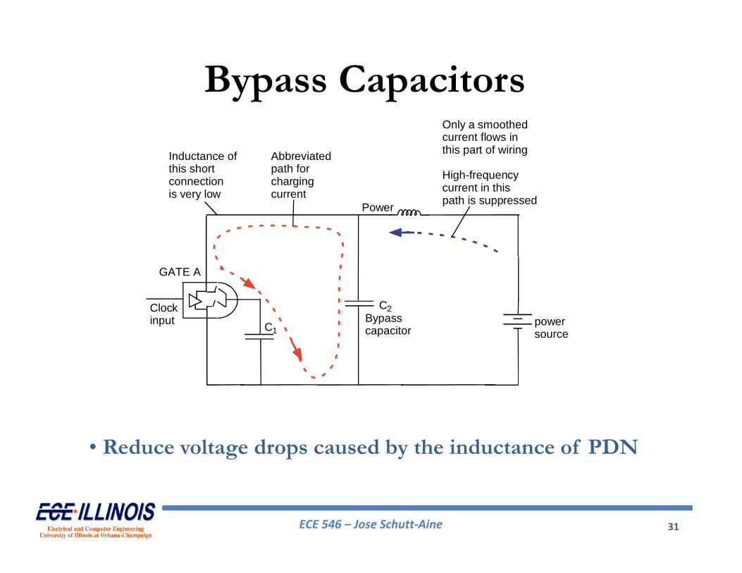
ECE 546 – Jose Schutt‐Aine 31
C1
Clockinput
Power
GATE A
C2Bypasscapacitor
powersource
Abbreviatedpath forchargingcurrent
Inductance ofthis shortconnectionis very low
Only a smoothedcurrent flows inthis part of wiring
High-frequencycurrent in thispath is suppressed
Bypass Capacitors
• Reduce voltage drops caused by the inductance of PDN
ECE 546 – Jose Schutt‐Aine 32
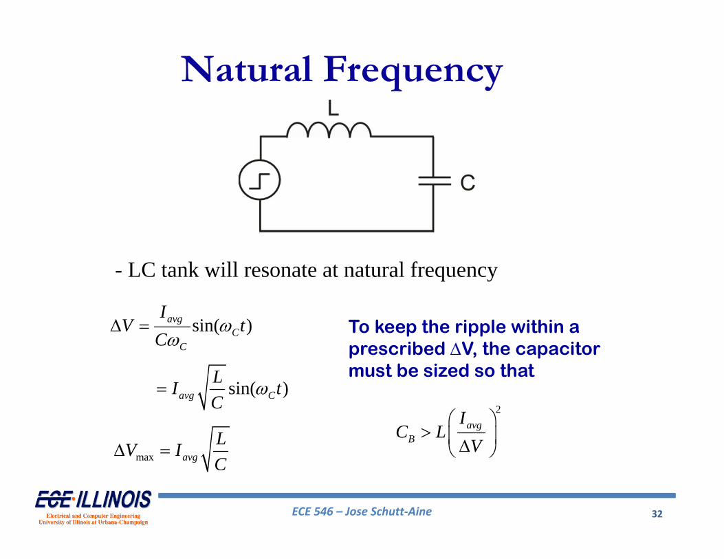
- LC tank will resonate at natural frequency
sin( )avgC
C
IV t
C
sin( )avg CLI tC
max avgLV IC
Natural Frequency
To keep the ripple within a prescribed V, the capacitor must be sized so that
2avg
B
IC L
V
ECE 546 – Jose Schutt‐Aine 33
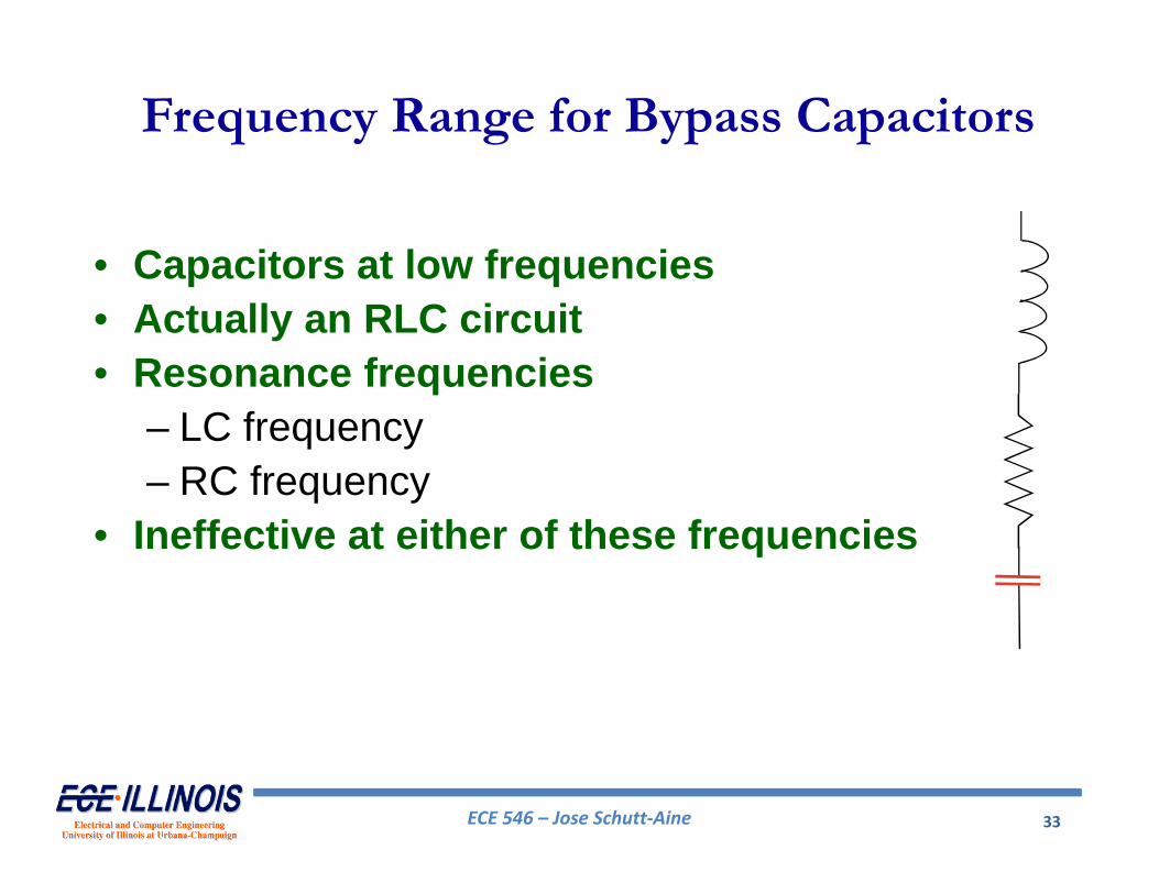
Frequency Range for Bypass Capacitors
• Capacitors at low frequencies• Actually an RLC circuit• Resonance frequencies
– LC frequency– RC frequency
• Ineffective at either of these frequencies
ECE 546 – Jose Schutt‐Aine 34
• Load currents at frequencies well below c see an inductive impedance.
• Load currents at high frequencies see a capacitor.
• At c, impedance is infinite
• At c, even small currents will cause oscillations
Natural Frequency of Bypass Capacitors
ECE 546 – Jose Schutt‐Aine 35
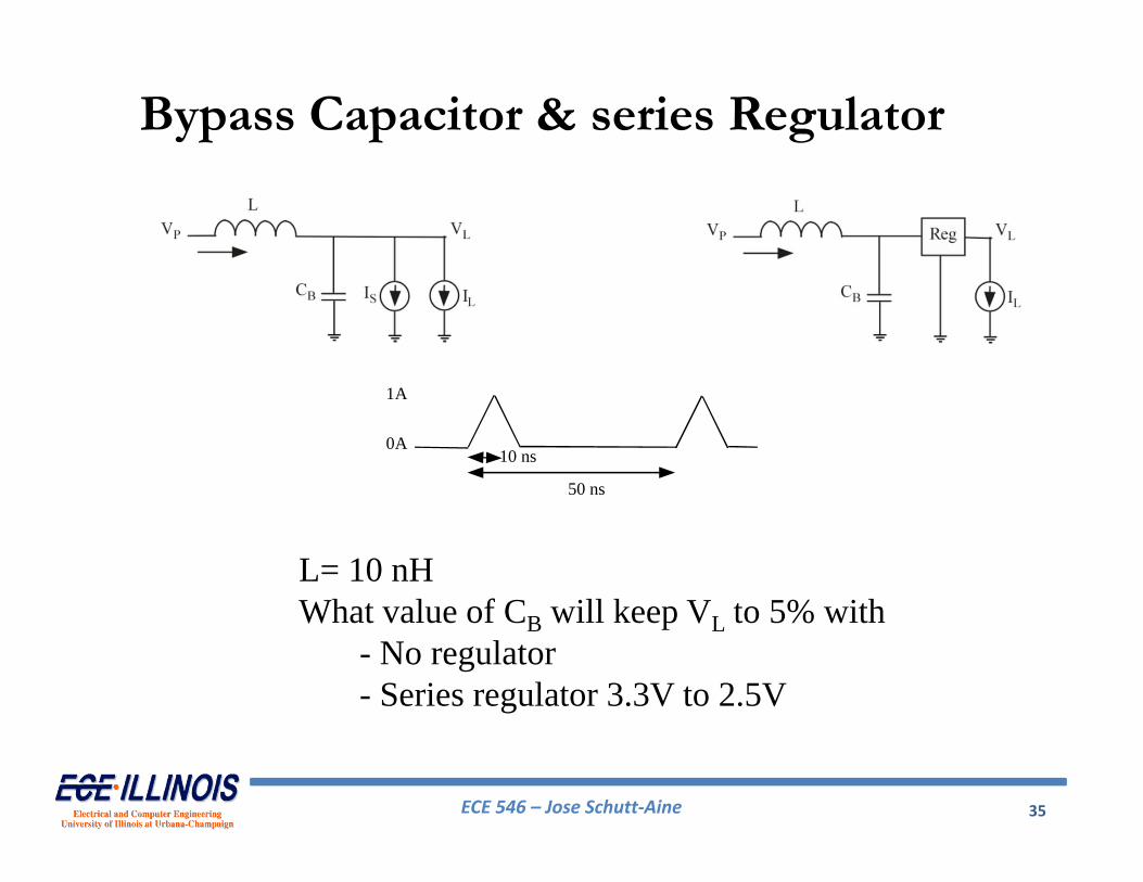
L= 10 nHWhat value of CB will keep VL to 5% with
- No regulator- Series regulator 3.3V to 2.5V
Bypass Capacitor & series Regulator
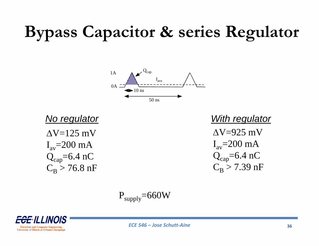
1A
0A
50 ns
10 ns
ECE 546 – Jose Schutt‐Aine 36
V=125 mVIav=200 mAQcap=6.4 nCCB > 76.8 nF
V=925 mVIav=200 mAQcap=6.4 nCCB > 7.39 nF
Psupply=660W
Bypass Capacitor & series Regulator
Qcap1A
0A10 ns
Iavs
50 ns
No regulator With regulator
ECE 546 – Jose Schutt‐Aine 37
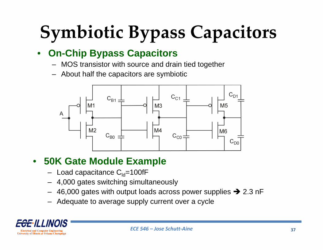
Symbiotic Bypass Capacitors
• 50K Gate Module Example– Load capacitance Cld=100fF– 4,000 gates switching simultaneously– 46,000 gates with output loads across power supplies 2.3 nF– Adequate to average supply current over a cycle
• On-Chip Bypass Capacitors– MOS transistor with source and drain tied together– About half the capacitors are symbiotic
ECE 546 – Jose Schutt‐Aine 38
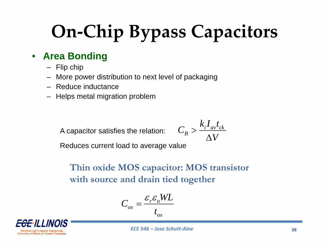
• Area Bonding– Flip chip– More power distribution to next level of packaging– Reduce inductance– Helps metal migration problem
A capacitor satisfies the relation: i av ckB
k I tCV
Reduces current load to average value
r oox
ox
WLCt
Thin oxide MOS capacitor: MOS transistor with source and drain tied together
On‐Chip Bypass Capacitors
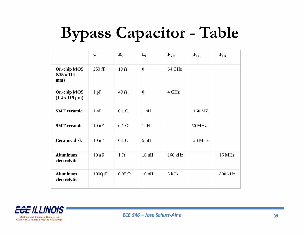
ECE 546 – Jose Schutt‐Aine 39
Bypass Capacitor - TableC RS LC FRC FLC FLR
On-chip MOS0.35 x 114 mm)
250 fF 10 0 64 GHz
On-chip MOS(1.4 x 115 m)
1 pF 40 0 4 GHz
SMT ceramic 1 nF 0.1 1 nH 160 MZ
SMT ceramic 10 nF 0.1 1nH 50 MHz
Ceramic disk 10 nF 0.1 5 nH 23 MHz
Aluminum electrolytic
10 F 1 10 nH 160 kHz 16 MHz
Aluminum electrolytic
1000F 0.05 10 nH 3 kHz 800 kHz
ECE 546 – Jose Schutt‐Aine 40
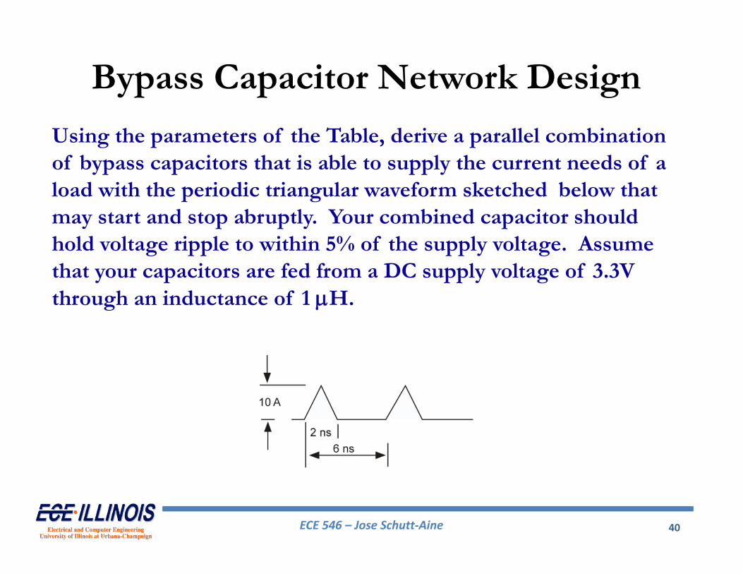
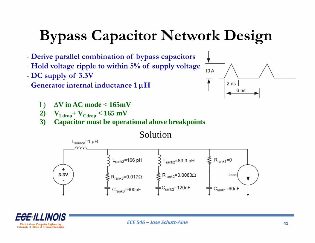
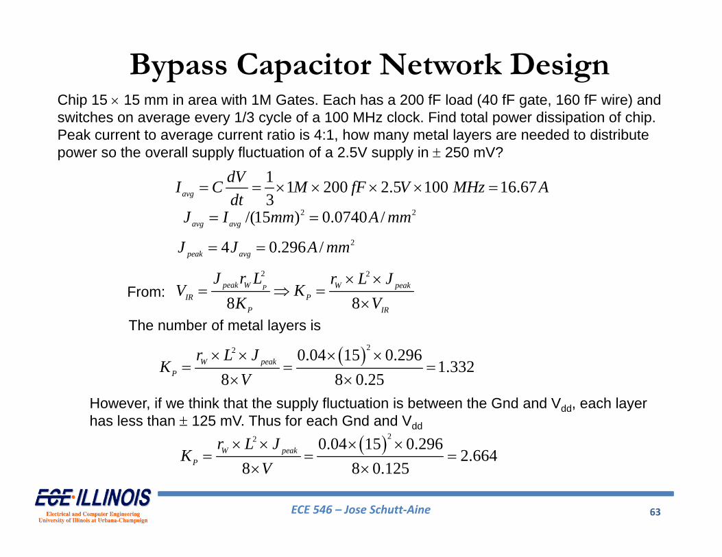
Using the parameters of the Table, derive a parallel combination of bypass capacitors that is able to supply the current needs of a load with the periodic triangular waveform sketched below that may start and stop abruptly. Your combined capacitor should hold voltage ripple to within 5% of the supply voltage. Assume that your capacitors are fed from a DC supply voltage of 3.3V through an inductance of 1 H.
Bypass Capacitor Network Design
ECE 546 – Jose Schutt‐Aine 41
- Derive parallel combination of bypass capacitors-Hold voltage ripple to within 5% of supply voltage- DC supply of 3.3V- Generator internal inductance 1 H
Solution
V in AC mode < 165mV2) VLdrop+ VCdrop < 165 mV3) Capacitor must be operational above breakpoints
Bypass Capacitor Network Design
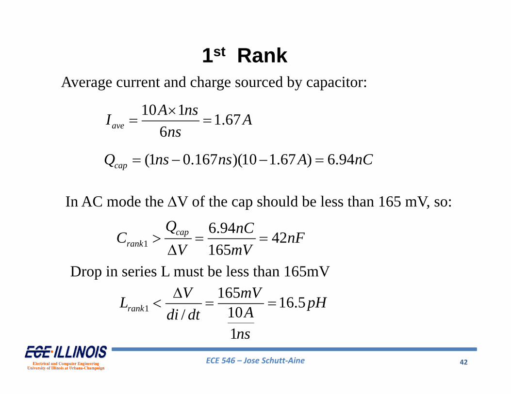
ECE 546 – Jose Schutt‐Aine 42
10 1 1.676aveA nsI A
ns
(1 0.167 )(10 1.67 ) 6.94capQ ns ns A nC
16.94 42165
caprank
Q nCC nFV mV
1165 16.510/
1
rankV mVL pHAdi dt
ns
Average current and charge sourced by capacitor:
In AC mode the V of the cap should be less than 165 mV, so:
Drop in series L must be less than 165mV
1st Rank
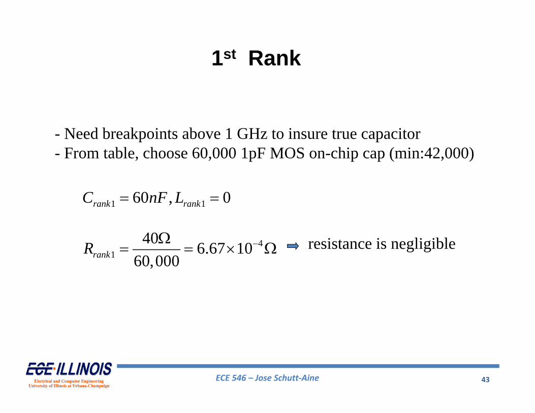
ECE 546 – Jose Schutt‐Aine 43
1 160 , 0rank rankC nF L
41
40 6.67 1060,000rankR
- Need breakpoints above 1 GHz to insure true capacitor- From table, choose 60,000 1pF MOS on-chip cap (min:42,000)
resistance is negligible
1st Rank
ECE 546 – Jose Schutt‐Aine 44
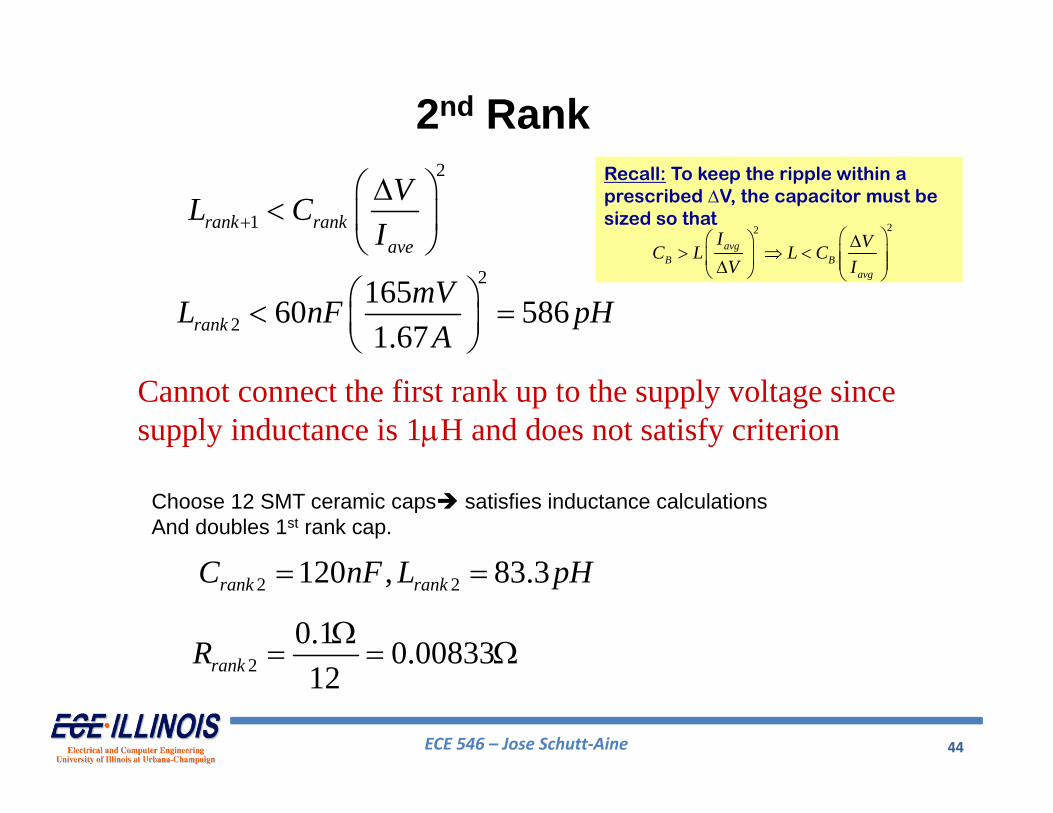
2
1rank rankave
VL CI
2
216560 5861.67rank
mVL nF pHA
2 2120 , 83.3rank rankC nF L pH
20.1 0.0083312rankR
2nd Rank
Cannot connect the first rank up to the supply voltage since supply inductance is 1H and does not satisfy criterion
Choose 12 SMT ceramic caps satisfies inductance calculationsAnd doubles 1st rank cap.
Recall: To keep the ripple within a prescribed V, the capacitor must be sized so that 22
avgB B
avg
I VC L L CV I
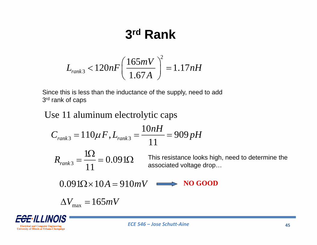
ECE 546 – Jose Schutt‐Aine 45
2
3165120 1.171.67rank
mVL nF nHA
3 310110 , 909
11rank ranknHC F L pH
31 0.09111rankR
0.091 10 910A mV
max 165V mV
3rd Rank
Since this is less than the inductance of the supply, need to add3rd rank of caps
Use 11 aluminum electrolytic caps
NO GOOD
This resistance looks high, need to determine theassociated voltage drop…
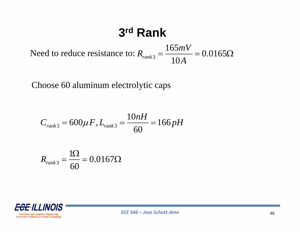
ECE 546 – Jose Schutt‐Aine 46
3165 0.0165
10rankmVRA
3 310600 , 166
60rank ranknHC F L pH
Need to reduce resistance to:
Choose 60 aluminum electrolytic caps
31 0.016760rankR
3rd Rank
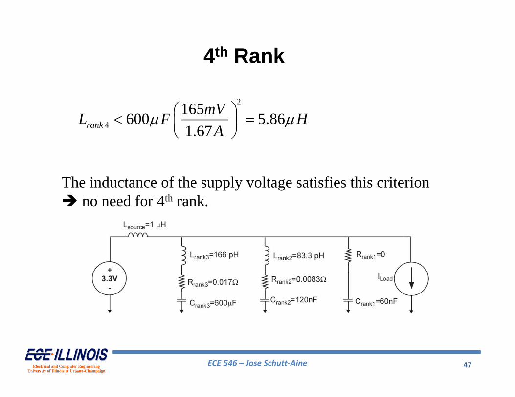
ECE 546 – Jose Schutt‐Aine 47
2
4165600 5.861.67rank
mVL F HA
4th Rank
The inductance of the supply voltage satisfies this criterion no need for 4th rank.
ECE 546 – Jose Schutt‐Aine 48
• Ground planes power bus and return paths are not ideal and must be represented with parasitic inductors and resistors
• Resulting network is a two-dimensional lossytransmission line possibly non-uniform
• Bypass capacitors are needed to alleviate noise
• Simulation is computationally intensive
Modeling Power Distribution Networks (PDN)
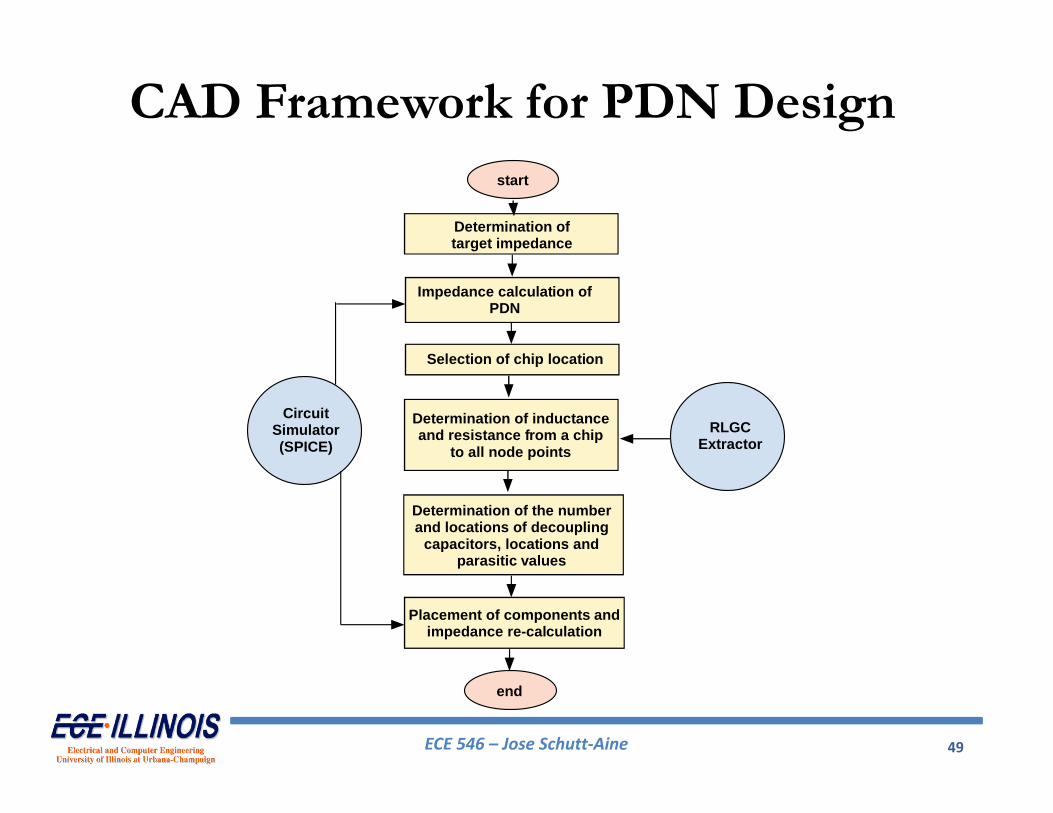
ECE 546 – Jose Schutt‐Aine 49
Determination of inductanceand resistance from a chip
to all node points
Impedance calculation ofPDN
Selection of chip location
Determination oftarget impedance
Determination of the numberand locations of decoupling
capacitors, locations andparasitic values
Placement of components andimpedance re-calculation
end
start
CircuitSimulator(SPICE)
RLGCExtractor
CAD Framework for PDN Design
ECE 546 – Jose Schutt‐Aine 50
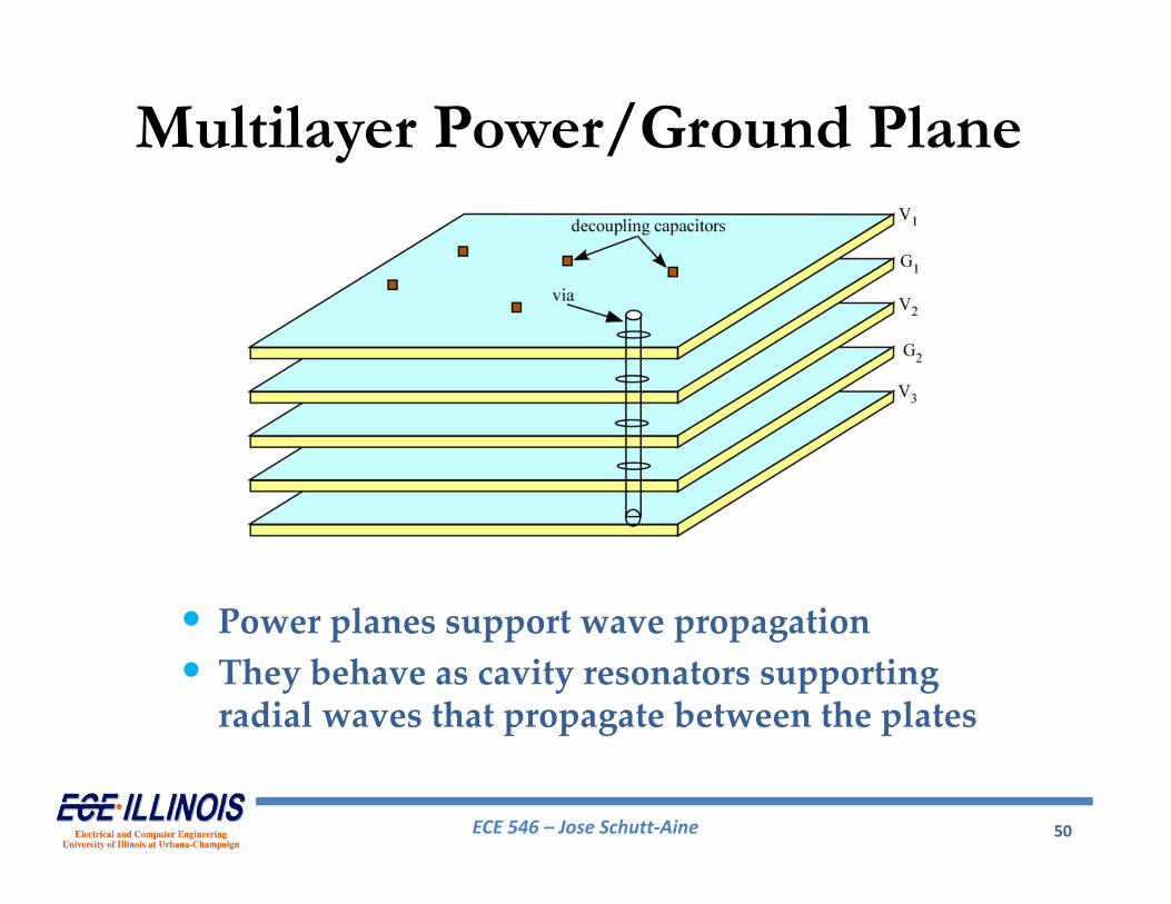
Multilayer Power/Ground Plane
• Power planes support wave propagation• They behave as cavity resonators supporting radial waves that propagate between the plates
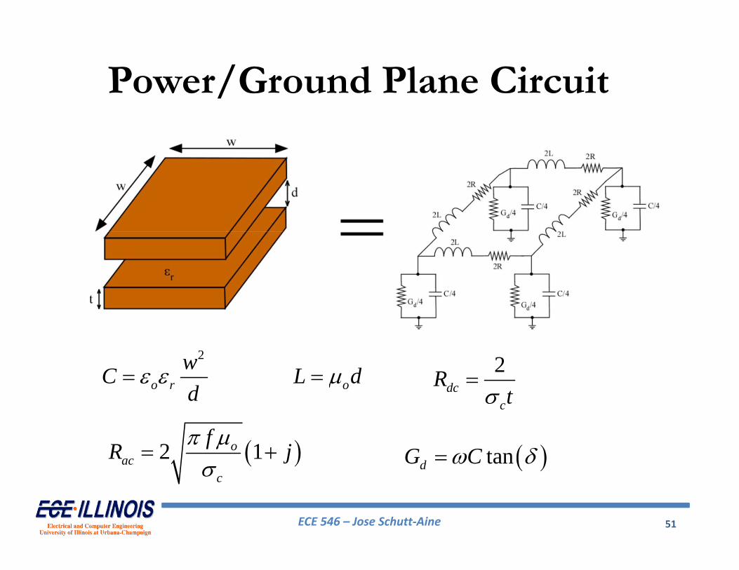
ECE 546 – Jose Schutt‐Aine 51
2
o rwCd
oL d 2dc
c
Rt
2 1oac
c
fR j
tandG C
Power/Ground Plane Circuit
ECE 546 – Jose Schutt‐Aine 5252
X cells
Y cells
+- +-
+
-
+- +-
+
-
+
-=Unit cell
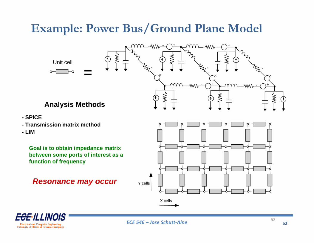
Example: Power Bus/Ground Plane Model
Resonance may occur
- SPICE- Transmission matrix method- LIM
Analysis Methods
Goal is to obtain impedance matrix between some ports of interest as a function of frequency
ECE 546 – Jose Schutt‐Aine 53
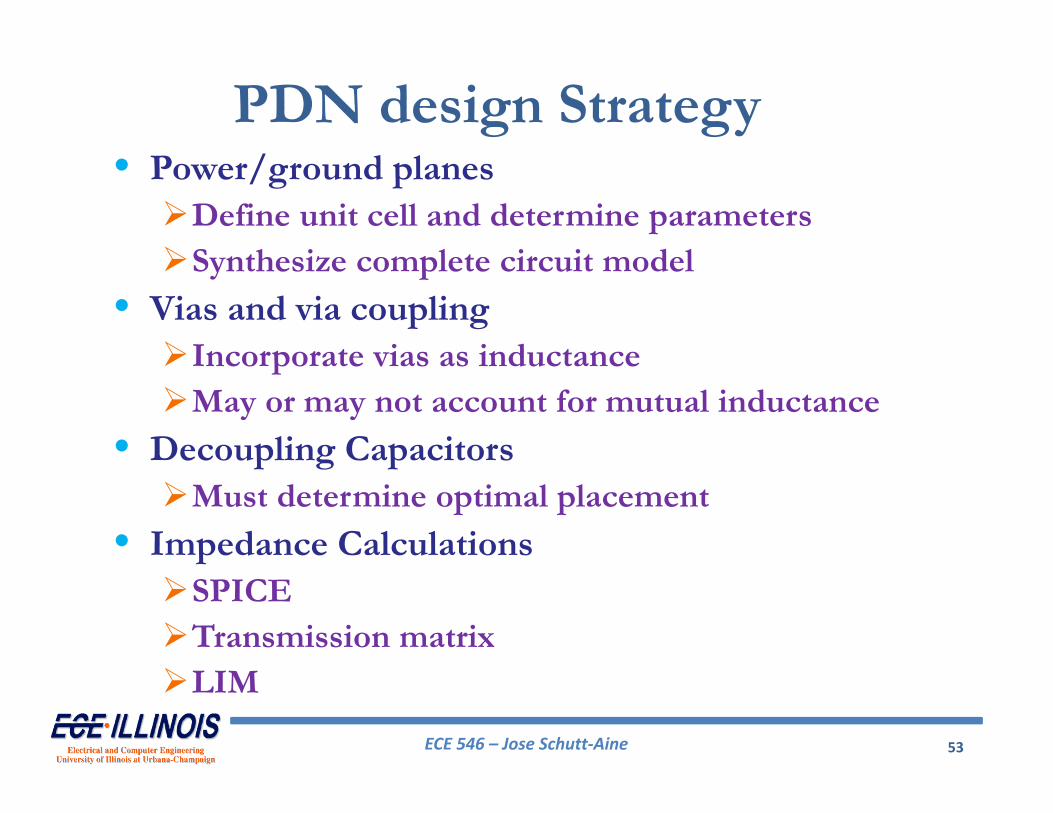
PDN design Strategy• Power/ground planesDefine unit cell and determine parametersSynthesize complete circuit model
• Vias and via couplingIncorporate vias as inductanceMay or may not account for mutual inductance
• Decoupling CapacitorsMust determine optimal placement
• Impedance CalculationsSPICETransmission matrixLIM
ECE 546 – Jose Schutt‐Aine 54
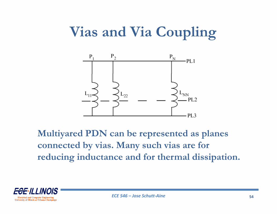
Vias and Via Coupling
Multiyared PDN can be represented as planes connected by vias. Many such vias are for reducing inductance and for thermal dissipation.
ECE 546 – Jose Schutt‐Aine 55
Decoupling Capacitors
ECE 546 – Jose Schutt‐Aine 56
Impedance Calculations
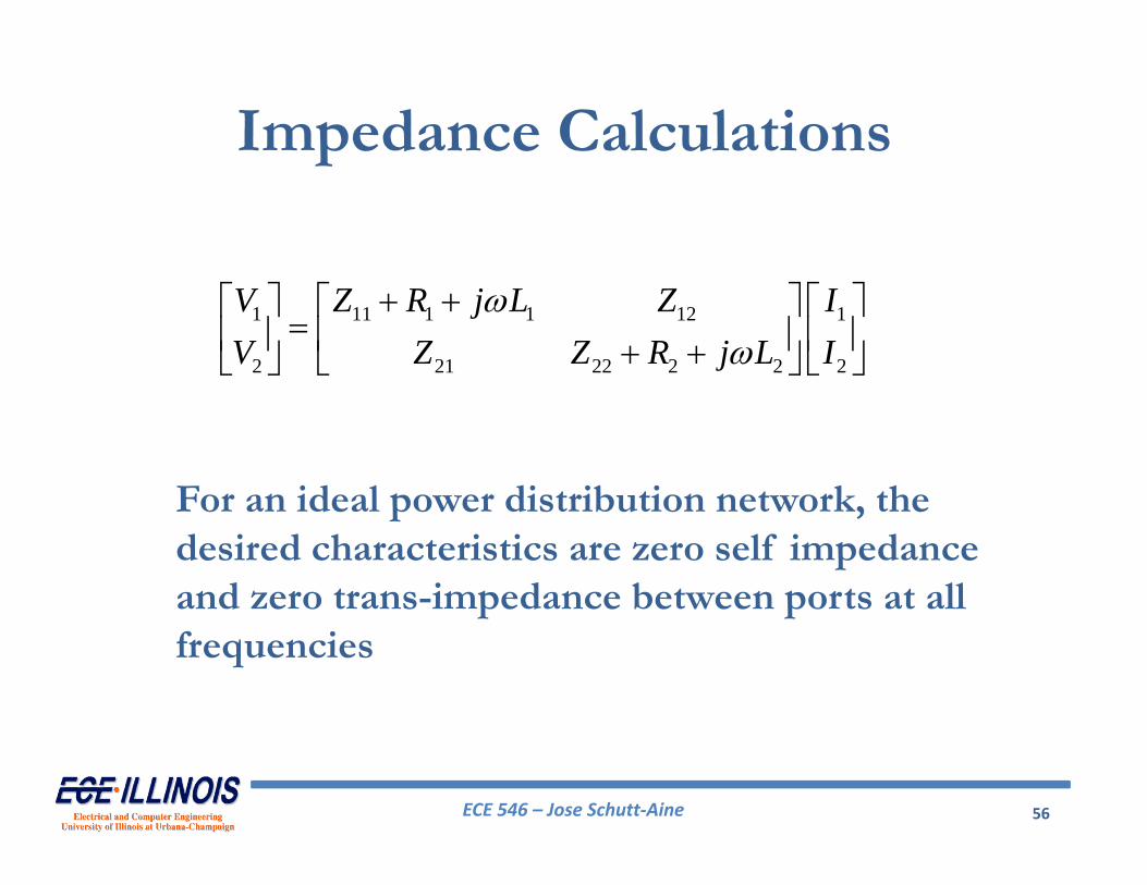
1 11 1 1 12 1
2 21 22 2 2 2
V Z R j L Z IV Z Z R j L I
For an ideal power distribution network, the desired characteristics are zero self impedance and zero trans-impedance between ports at all frequencies
ECE 546 – Jose Schutt‐Aine 57
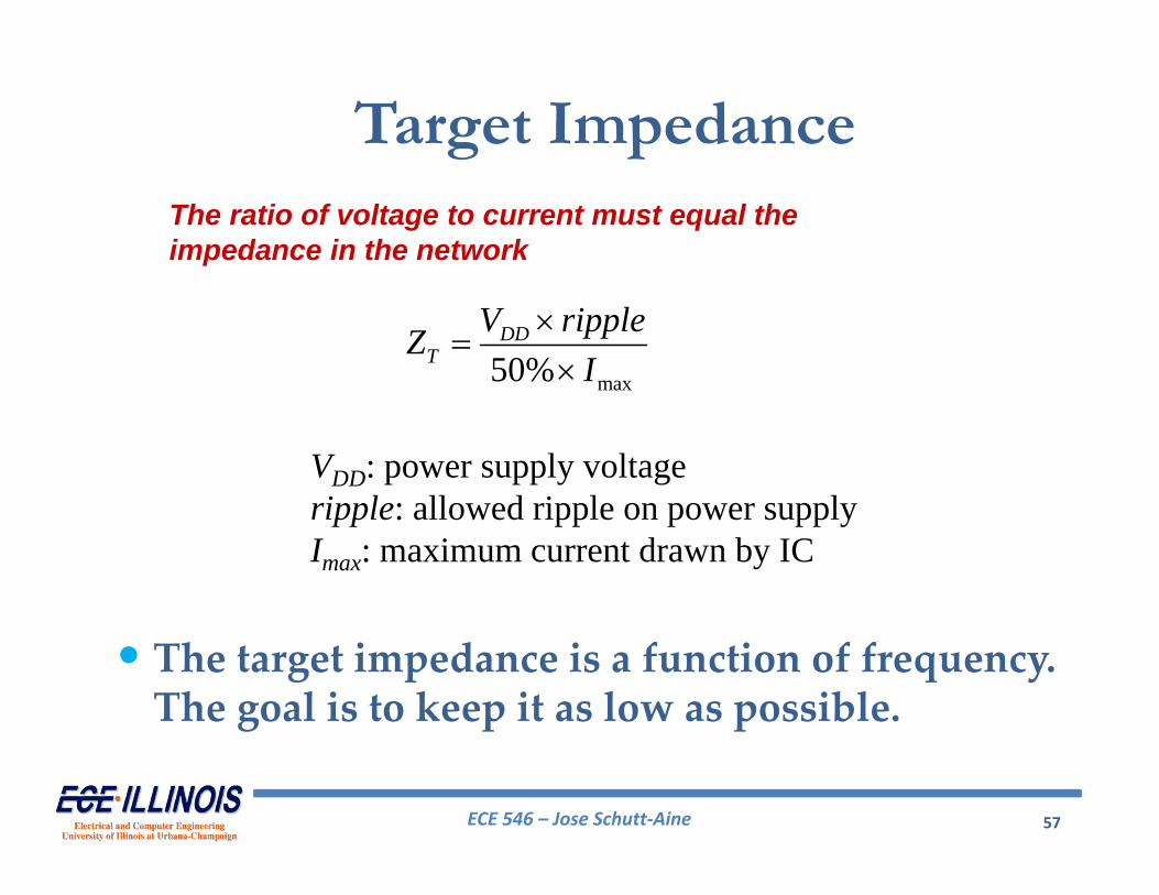
Target ImpedanceThe ratio of voltage to current must equal the impedance in the network
max50%DD
TV rippleZ
I
VDD: power supply voltageripple: allowed ripple on power supplyImax: maximum current drawn by IC
• The target impedance is a function of frequency. The goal is to keep it as low as possible.
ECE 546 – Jose Schutt‐Aine 58
Zo
Frequency
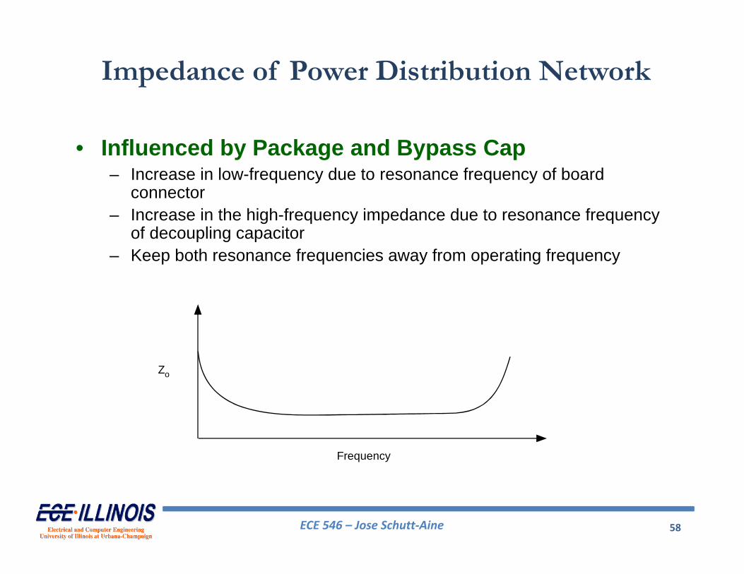
Impedance of Power Distribution Network
• Influenced by Package and Bypass Cap– Increase in low-frequency due to resonance frequency of board
connector– Increase in the high-frequency impedance due to resonance frequency
of decoupling capacitor– Keep both resonance frequencies away from operating frequency
ECE 546 – Jose Schutt‐Aine 59
VP Bus
VP Bus
VP Bus
VP Bus
VP Bus
GND Bus
GND Bus
GND Bus
GND Bus
VP
GND
Local Buses
Wiring Tracks
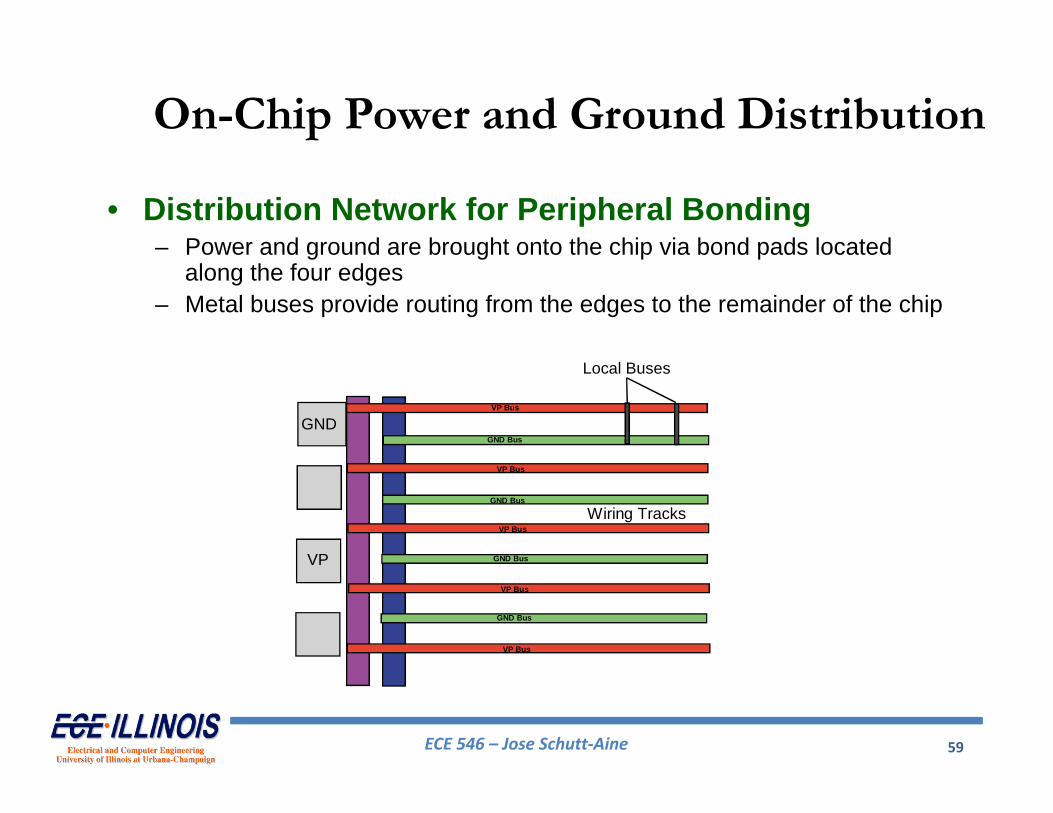
• Distribution Network for Peripheral Bonding– Power and ground are brought onto the chip via bond pads located
along the four edges– Metal buses provide routing from the edges to the remainder of the chip
On-Chip Power and Ground Distribution
ECE 546 – Jose Schutt‐Aine 60
INI5I4I3I2I1
RP RP RP RP RP RP
RP RP RP RP RPRP
VP
GND
V1 V1 V1 V1 V1 V1
2P w
PP
L rRNW
2
P PP
P
L WANk
2/ 2 / 2
21 1 4
PN N
pkIR pk P P
i i P
iJ L rV iJ A R
N k
2/ 2
0 8P P
L pk wpk wIR
P P
J r LJ r xV dx
k k
Model for On-Chip Power Distribution
wr : resistivity
: # of segments
: fraction of metal layer devoted to power buses
: Area
Pk
N
PAin continuum,
ECE 546 – Jose Schutt‐Aine 61
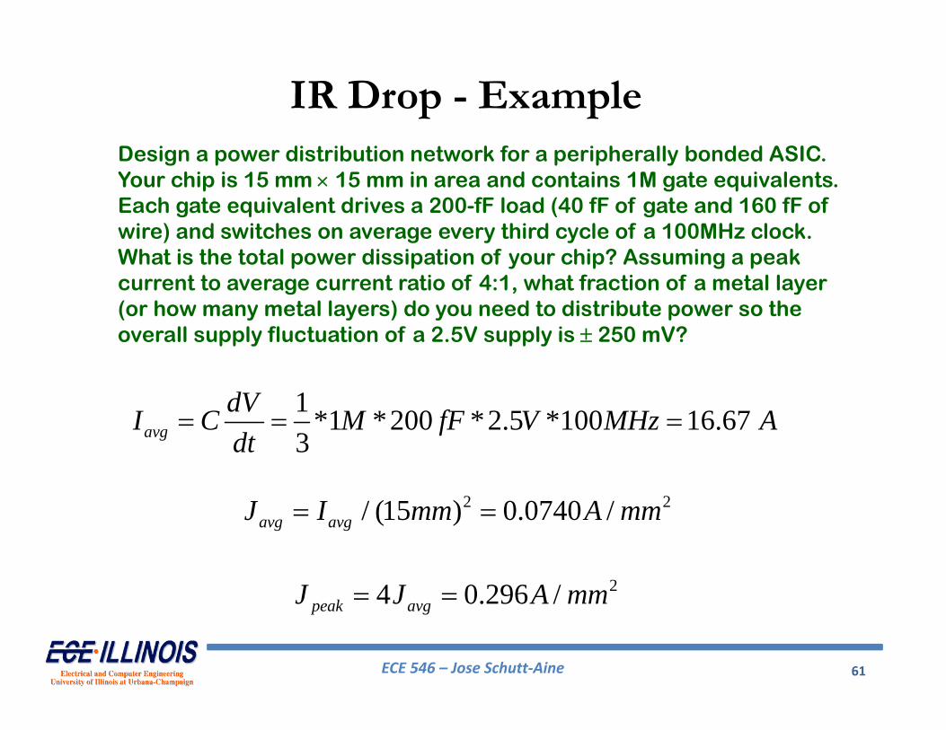
Design a power distribution network for a peripherally bonded ASIC. Your chip is 15 mm 15 mm in area and contains 1M gate equivalents. Each gate equivalent drives a 200-fF load (40 fF of gate and 160 fF of wire) and switches on average every third cycle of a 100MHz clock. What is the total power dissipation of your chip? Assuming a peak current to average current ratio of 4:1, what fraction of a metal layer (or how many metal layers) do you need to distribute power so the overall supply fluctuation of a 2.5V supply is 250 mV?
1 *1 *200 *2.5 *100 16.673avg
dVI C M fF V MHz Adt
2 2/ (15 ) 0.0740 /avg avgJ I mm A mm
24 0.296 /peak avgJ J A mm
IR Drop - Example
ECE 546 – Jose Schutt‐Aine 62
22 0.04 15 0.2961.332
8 8 0.25W peak
p
r L JK
V
IR Drop
Therefore, the number of metal layers is
If actual supply fluctuation is between Gnd and Vdd, each layer has less than 125mV fluctuation. Therefore, for each Gnd and Vdd,
22 0.04 15 0.2962.664
8 8 0.125W peak
p
r L JK
V
ECE 546 – Jose Schutt‐Aine 63
Chip 15 15 mm in area with 1M Gates. Each has a 200 fF load (40 fF gate, 160 fF wire) and switches on average every 1/3 cycle of a 100 MHz clock. Find total power dissipation of chip. Peak current to average current ratio is 4:1, how many metal layers are needed to distribute power so the overall supply fluctuation of a 2.5V supply in 250 mV?
1 1 200 2.5 100 16.673avg
dVI C M fF V MHz Adt
2 2/(15 ) 0.0740 /avg avgJ I mm A mm
24 0.296 /peak avgJ J A mm
22 0.04 15 0.2961.332
8 8 0.25W peak
P
r L JK
V
22 0.04 15 0.2962.664
8 8 0.125W peak
P
r L JK
V
2 2
8 8Ppeak W W peak
IR PP IR
J r L r L JV K
K V
The number of metal layers is
However, if we think that the supply fluctuation is between the Gnd and Vdd, each layer has less than 125 mV. Thus for each Gnd and Vdd
From:
Bypass Capacitor Network Design
ECE 546 – Jose Schutt‐Aine 64
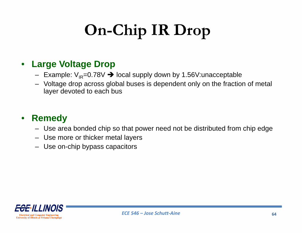
On-Chip IR Drop
• Large Voltage Drop– Example: VIR=0.78V local supply down by 1.56V:unacceptable– Voltage drop across global buses is dependent only on the fraction of metal
layer devoted to each bus
• Remedy– Use area bonded chip so that power need not be distributed from chip edge– Use more or thicker metal layers– Use on-chip bypass capacitors
ECE 546 – Jose Schutt‐Aine 65
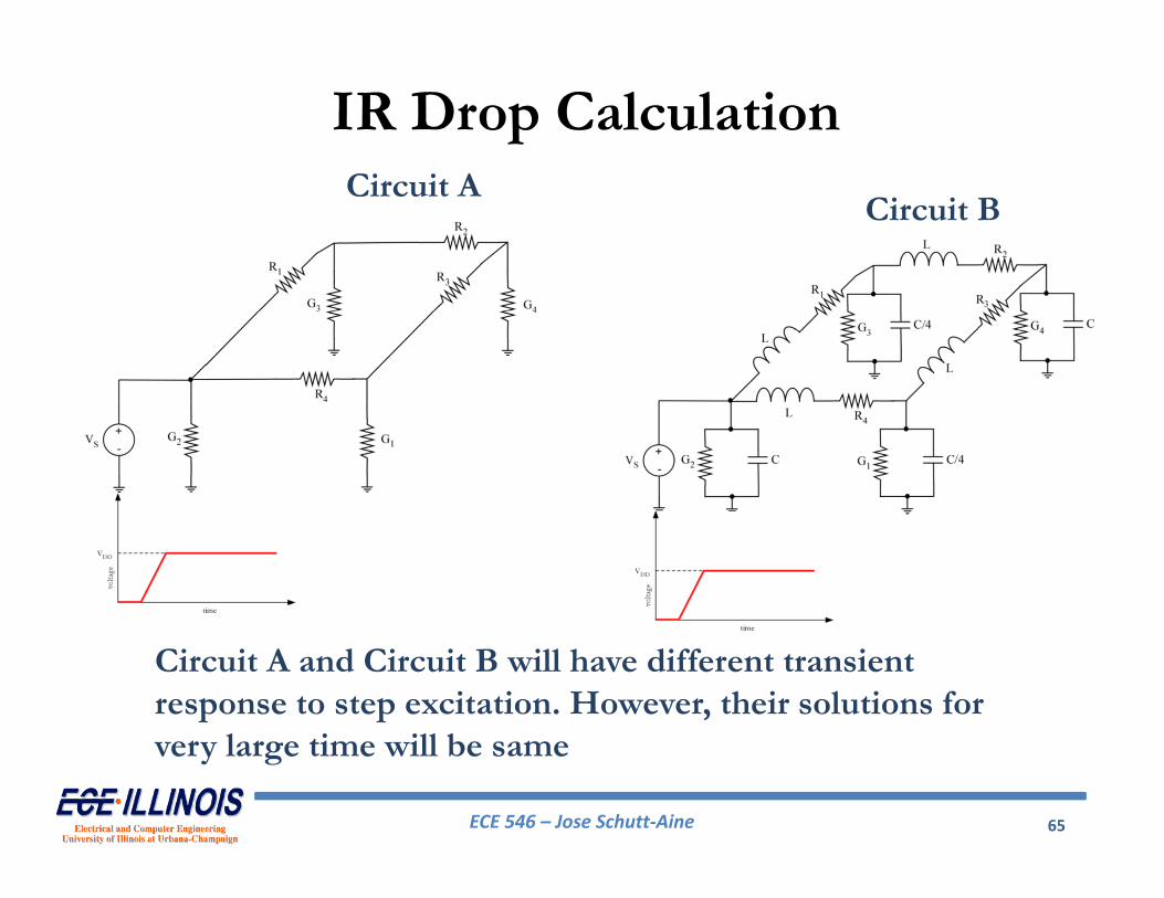
Circuit ACircuit B
Circuit A and Circuit B will have different transient response to step excitation. However, their solutions for very large time will be same
IR Drop Calculation
ECE 546 – Jose Schutt‐Aine 66
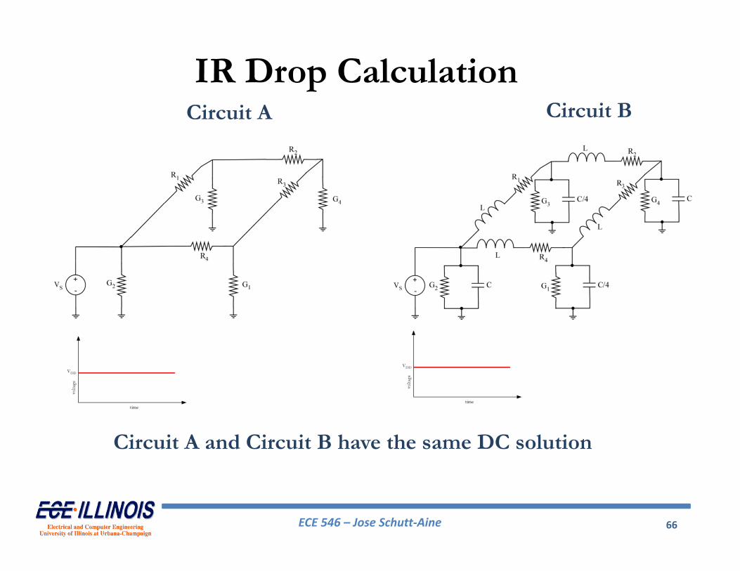
Circuit A Circuit B
Circuit A and Circuit B have the same DC solution
IR Drop Calculation
ECE 546 – Jose Schutt‐Aine 67
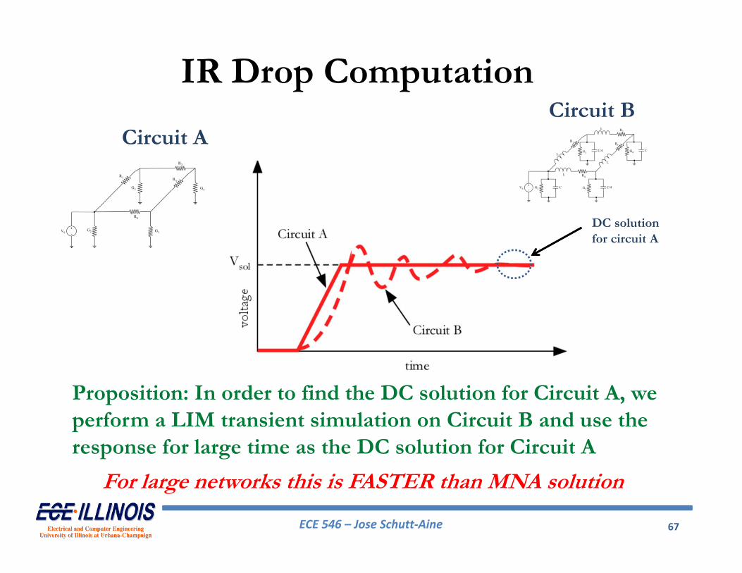
Circuit ACircuit B
Proposition: In order to find the DC solution for Circuit A, we perform a LIM transient simulation on Circuit B and use the response for large time as the DC solution for Circuit A
DC solution for circuit A
IR Drop Computation
For large networks this is FASTER than MNA solution
ECE 546 – Jose Schutt‐Aine 68
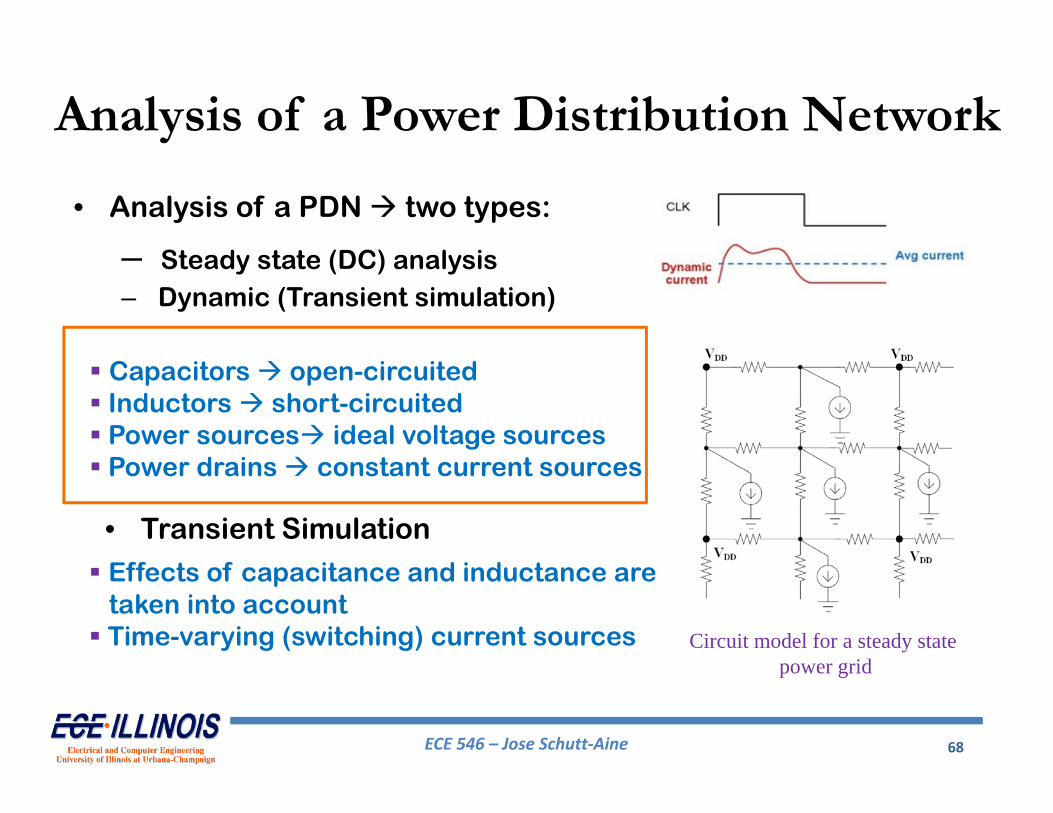
Analysis of a Power Distribution Network
• Analysis of a PDN two types:
– Steady state (DC) analysis– Dynamic (Transient simulation)
Circuit model for a steady statepower grid
Capacitors open-circuited Inductors short-circuited Power sources ideal voltage sources Power drains constant current sources
Effects of capacitance and inductance aretaken into account Time-varying (switching) current sources
• Transient Simulation
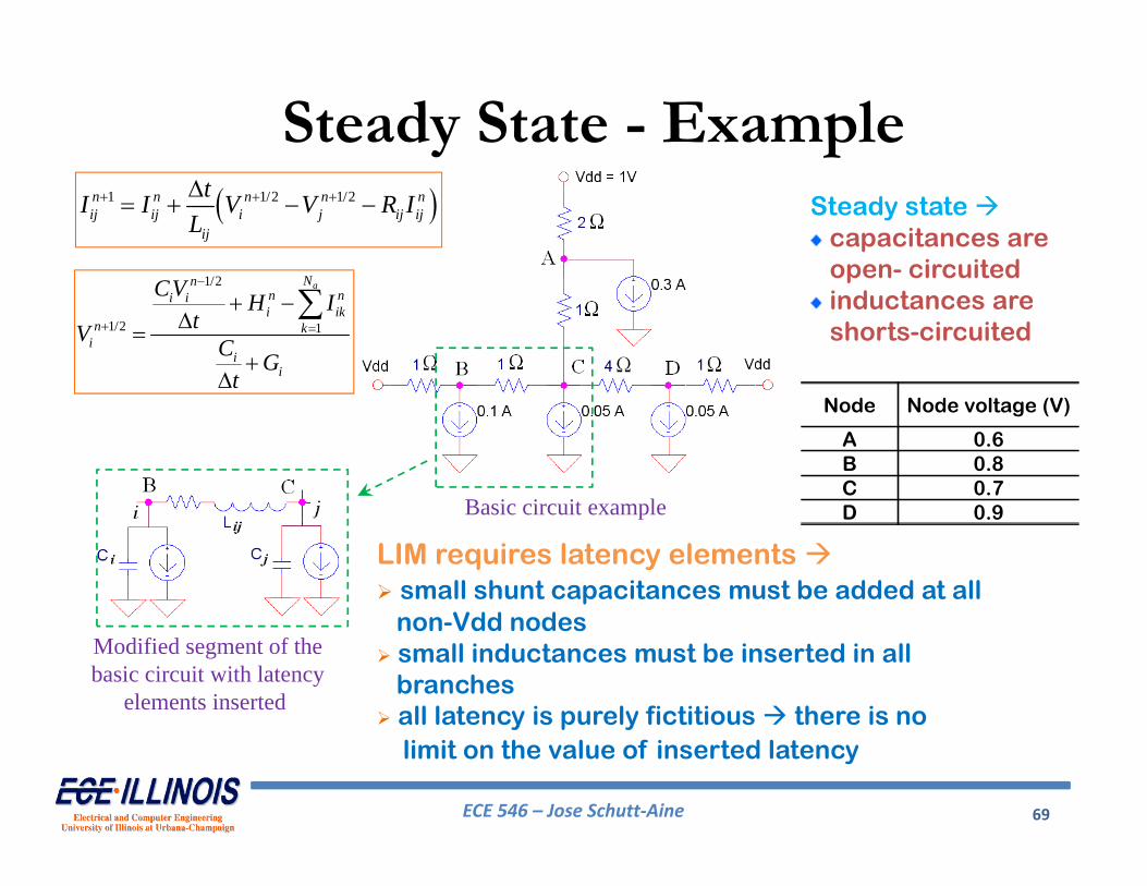
ECE 546 – Jose Schutt‐Aine 69
Steady State - Example
Node Node voltage (V)
A 0.6B 0.8C 0.7D 0.9
LIM requires latency elements small shunt capacitances must be added at all
non-Vdd nodes small inductances must be inserted in all
branches all latency is purely fictitious there is no
limit on the value of inserted latency
Basic circuit example
Modified segment of the basic circuit with latency
elements inserted
1 1/2 1/2n n n n nij ij i j ij ij
ij
tI I V V R IL
1/2
1/2 1
aNnn ni ii ik
n ki
ii
CV H ItV C G
t
Steady state capacitances areopen- circuitedinductances areshorts-circuited
ECE 546 – Jose Schutt‐Aine 70
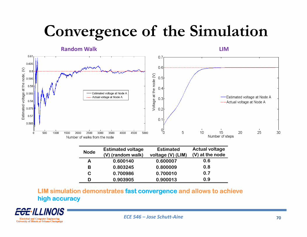
Convergence of the Simulation
NodeEstimated voltage (V) (random walk)
Estimated voltage (V) (LIM)
Actual voltage (V) at the node
A 0.600140 0.600007 0.6B 0.803245 0.800009 0.8C 0.700986 0.700010 0.7D 0.903905 0.900013 0.9
Random Walk LIM
LIM simulation demonstrates fast convergence and allows to achieve high accuracy
ECE 546 – Jose Schutt‐Aine 71
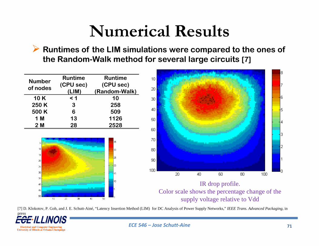
Numerical Results Runtimes of the LIM simulations were compared to the ones of
the Random-Walk method for several large circuits [7]
Number of nodes
Runtime (CPU sec)
(LIM)
Runtime (CPU sec)
(Random-Walk)10 K < 1 10
250 K 3 258500 K 6 509
1 M 13 11262 M 28 2528
IR drop profile. Color scale shows the percentage change of the
supply voltage relative to Vdd [7] D. Klokotov, P. Goh, and J. E. Schutt-Ainé, “Latency Insertion Method (LIM) for DC Analysis of Power Supply Networks,” IEEE Trans. Advanced Packaging, in press


