Ashenden, The Designer's Guide to VHDL2nd Edition, Morgan Kaufmann, 2001
• Recommended Text:
Mano and Kime, Logic and Computer Design Fundamentals, 3rd Edition Prentice Hall, 2004
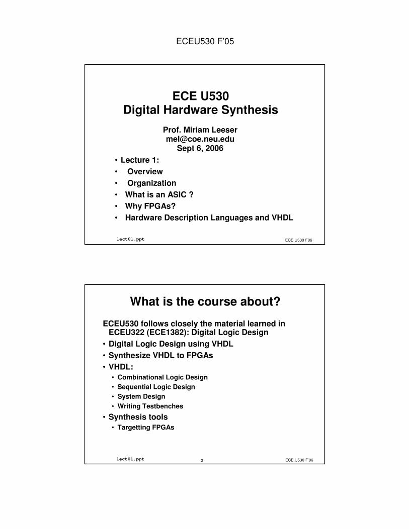
ECEU530 F’05
ECE U530 F’065lect01.ppt
Programming Assignments• All assignments are expected to represent individual
work !• Programming Assignments will be submitted
electronically. Tools:• Xilinx ISE version 6.2i • Modelsim 5.7e
• Programming assignments will be done on WinCOEsystems. Computers are available on the second floor of Snell Engineering.
• You must have a COE account for this class:• Go to http://www.coe.neu.edu/computer/
then click on HELP!then click on Account Information For New Users
ECE U530 F’066lect01.ppt
Programming Assignments• I have the tools (at work) on a PC. Can I work there, • then upload the tools ?• Yes, but ...
It is your responsibility to make sure:1. You are using the same version of the tools:• Version 6.2i of the Xilinx ISE tools• Version 5.7e of Modelsim
2. Your programs run under the WinCOE toolsi.e. no problems with formatting, etc.
You can download evaluation versions from Xilinx and Modelsim. These are newer versions of the tools. YOU MUST MAKE SURE YOUR ANSWERS WORK on the WinCOE system !!
ECEU530 F’05
ECE U530 F’067lect01.ppt
Policies: Grading• Midterm Exam (30%)
• Midterm Exam in class Tuesday, November 1
• Homework and Programming Assignments (30%)• Frequent homeworks (1 or 2 per week)• most will be programming assigments using
Xilinx and Modelsim
• Final Project (30%)December 13 at 1:00pm
ECE U530 F’068lect01.ppt
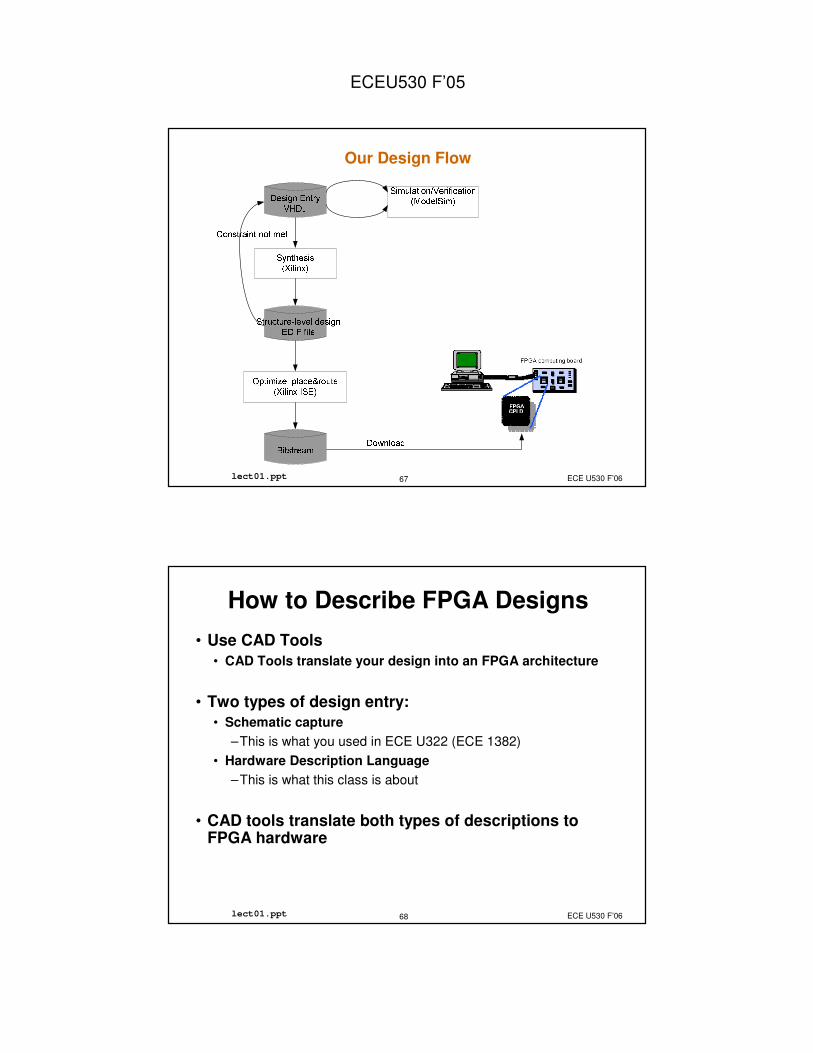
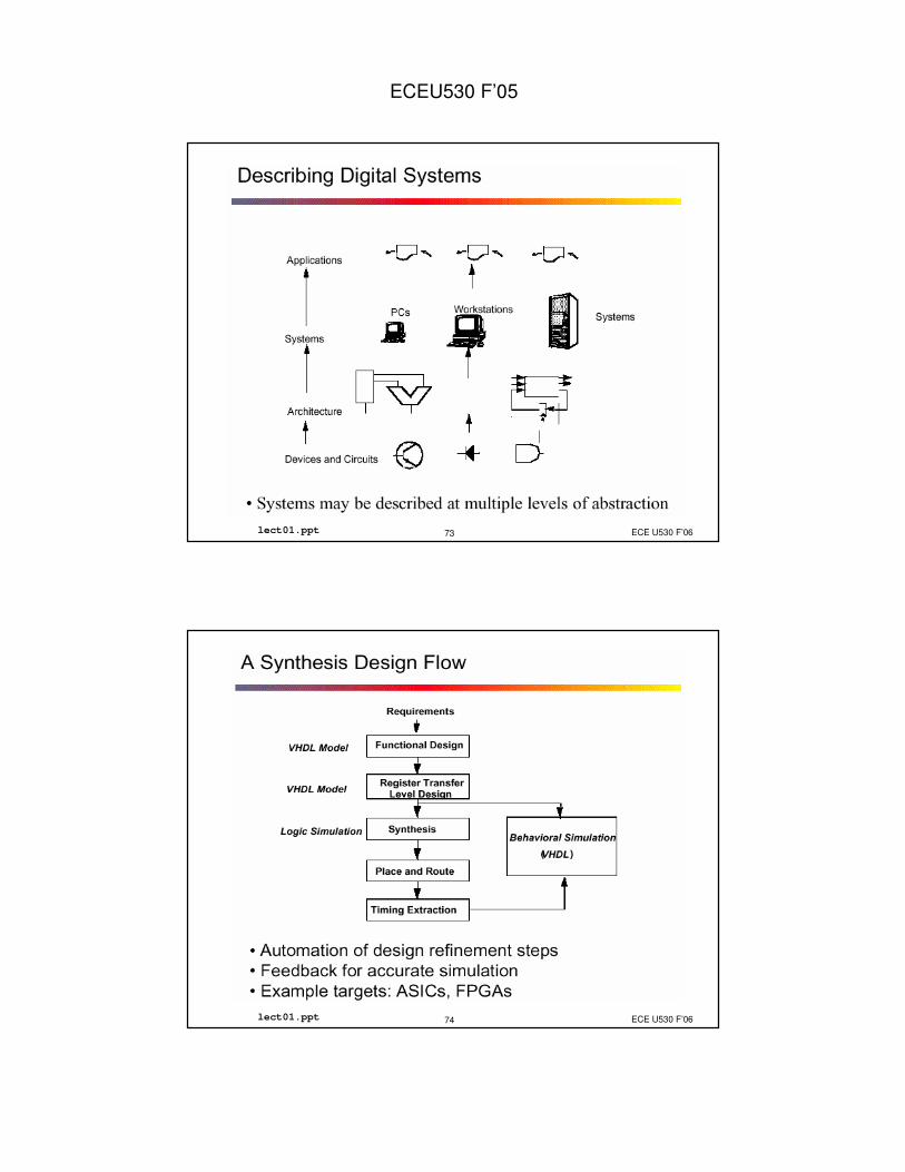
Our Design Flow
ECEU530 F’05
ECE U530 F’069lect01.ppt
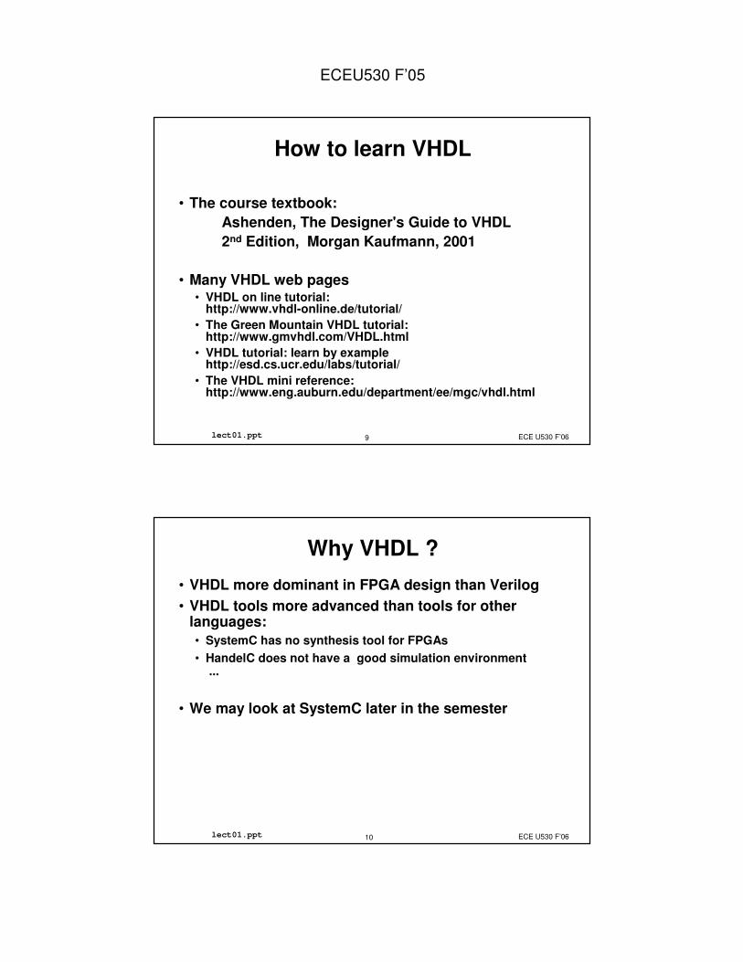
How to learn VHDL
• The course textbook:Ashenden, The Designer's Guide to VHDL2nd Edition, Morgan Kaufmann, 2001
• Many VHDL web pages• VHDL on line tutorial:
http://www.vhdl-online.de/tutorial/• The Green Mountain VHDL tutorial:
http://www.gmvhdl.com/VHDL.html• VHDL tutorial: learn by example
http://esd.cs.ucr.edu/labs/tutorial/• The VHDL mini reference:
Why VHDL ?• VHDL more dominant in FPGA design than Verilog• VHDL tools more advanced than tools for other
languages:• SystemC has no synthesis tool for FPGAs • HandelC does not have a good simulation environment
...
• We may look at SystemC later in the semester
ECEU530 F’05
ECE U530 F’0611lect01.ppt
An Integrated Circuit
•Measurement of chip size, gate count: the number of logic gates•A logic gate = a two-input NAND gate
Pin-grid array (PGA) packageWafer (holding hundreds of dice)
Silicon die or chip
ECE U530 F’0612lect01.ppt
CMOS is based on a MOSFET
p-well
n+ n+
L
Oxide (SiO2)
Polysilicon
W
Metal
The smallest feature size, λ=L/2 (unit: micron or µm)e.g., λ=0.25 µm in a 0.5 micron process
ECEU530 F’05
ECE U530 F’0613lect01.ppt
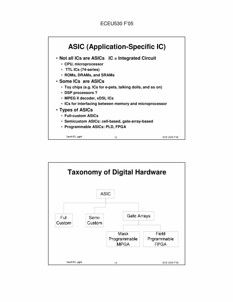
ASIC (Application-Specific IC)• Not all ICs are ASICs IC = Integrated Circuit
• CPU, microprocessor• TTL ICs (74-series)• ROMs, DRAMs, and SRAMs
• Some ICs are ASICs• Toy chips (e.g. ICs for e-pets, talking dolls, and so on)• DSP processors ?• MPEG II decoder, xDSL ICs• ICs for interfacing between memory and microprocessor
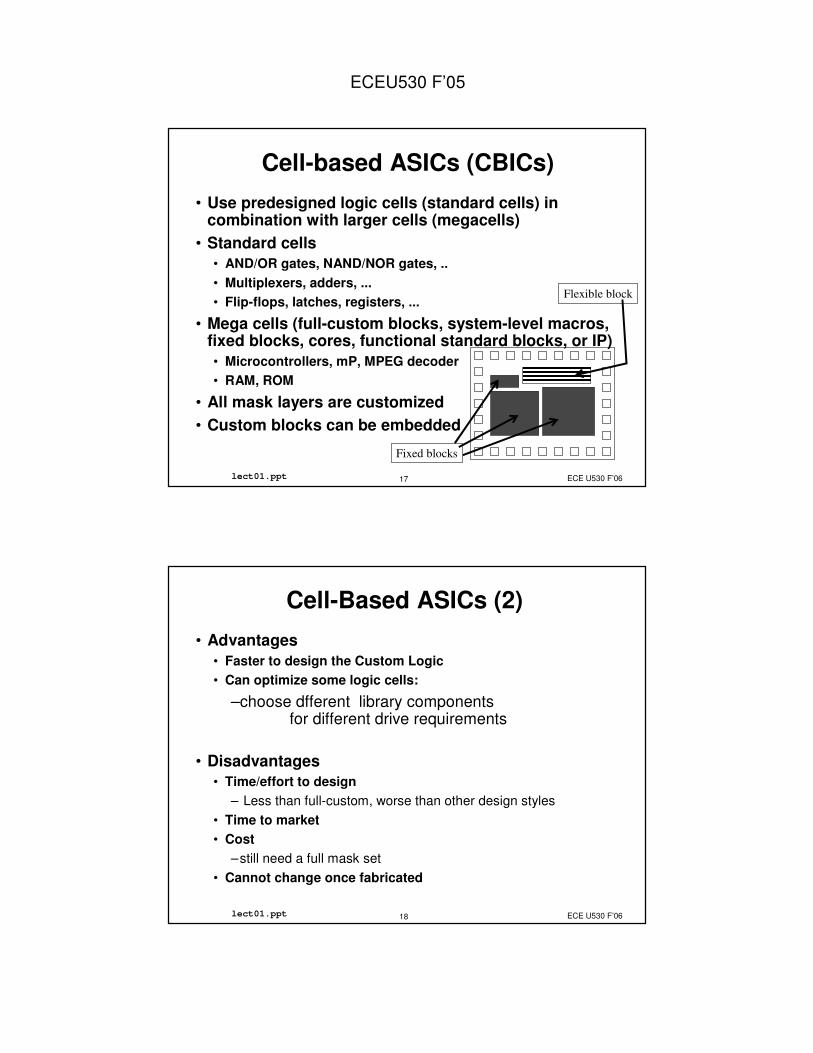
• Mega cells (full-custom blocks, system-level macros, fixed blocks, cores, functional standard blocks, or IP)• Microcontrollers, mP, MPEG decoder• RAM, ROM
• All mask layers are customized• Custom blocks can be embedded
ECE U530 F’0618lect01.ppt
Cell-Based ASICs (2) • Advantages
• Faster to design the Custom Logic• Can optimize some logic cells:
–choose dfferent library components for different drive requirements
• Disadvantages• Time/effort to design
– Less than full-custom, worse than other design styles• Time to market• Cost
–still need a full mask set• Cannot change once fabricated
ECEU530 F’05
ECE U530 F’0619lect01.ppt
Gate-Array Based ASICs• Gate array (or prediffused array)
• Transistors are predifined on the silicon wafer• Base array: the predifined pattern of transistors• Base cell: the smalles element that is replicated to make the
base array
• Masked gate array (MGA)• Only the top few layers of metal are defined by the designer
using custom masks• The designer chooses from a gate-array library of
predesigned logic cells (macros)
• Types of MGA ASICs• Channeled gate arrays• Channelless gate arrays• Structured gate arrays
ECE U530 F’0620lect01.ppt
Gate-Array Based ASICs (2) • Advantages
• Faster to design the Semi-custom Logic• Lower cost
–only need top few layers of mask• Lower fabrication time
• Disadvantages• Cannot optimize for performance• Time to market
– faster than CBICs, slower than FPGAs• Cannot change once fabricated
ECEU530 F’05
ECE U530 F’0621lect01.ppt
Programmable Logic• Not all programmable logic is FIELD programmable• PLAs and PALs implement AND-OR logic• Useful for implementing combinational logic• PLA : Programmable Logic Array
• programmable AND, programmable OR Planes
• PAL: Programmable Array Logic• programmable AND, fixed OR plane
• PLAs and PALs• similar architectures• “Programmable” by adding connections• May be mask programmable or field programmable depending
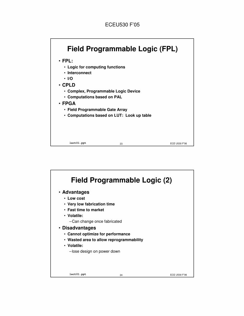
• Logic for computing functions• Interconnect• I/O
• CPLD• Complex, Programmable Logic Device• Computations based on PAL
• FPGA• Field Programmable Gate Array• Computations based on LUT: Look up table
ECE U530 F’0624lect01.ppt
Field Programmable Logic (2) • Advantages
• Low cost • Very low fabrication time• Fast time to market • Volatile:
–Can change once fabricated
• Disadvantages• Cannot optimize for performance• Wasted area to allow reprogrammability• Volatile:
–lose design on power down
ECEU530 F’05
ECE U530 F’0625lect01.ppt
FPGA•FPGAs do not contain AND or OR planes•Three elements:
• Logic blocks• I/O blocks• Interconnection wires and
switches
�����
�����
�
�����
� �������� ���
��� ����
ECE U530 F’0626lect01.ppt
Lookup Table (LUT)
%&�
%&�
%&�
%&�
��
��
�
111
001
010
100
fx2x1
�
%
%
�
��
��
�
ECEU530 F’05
ECE U530 F’0627lect01.ppt
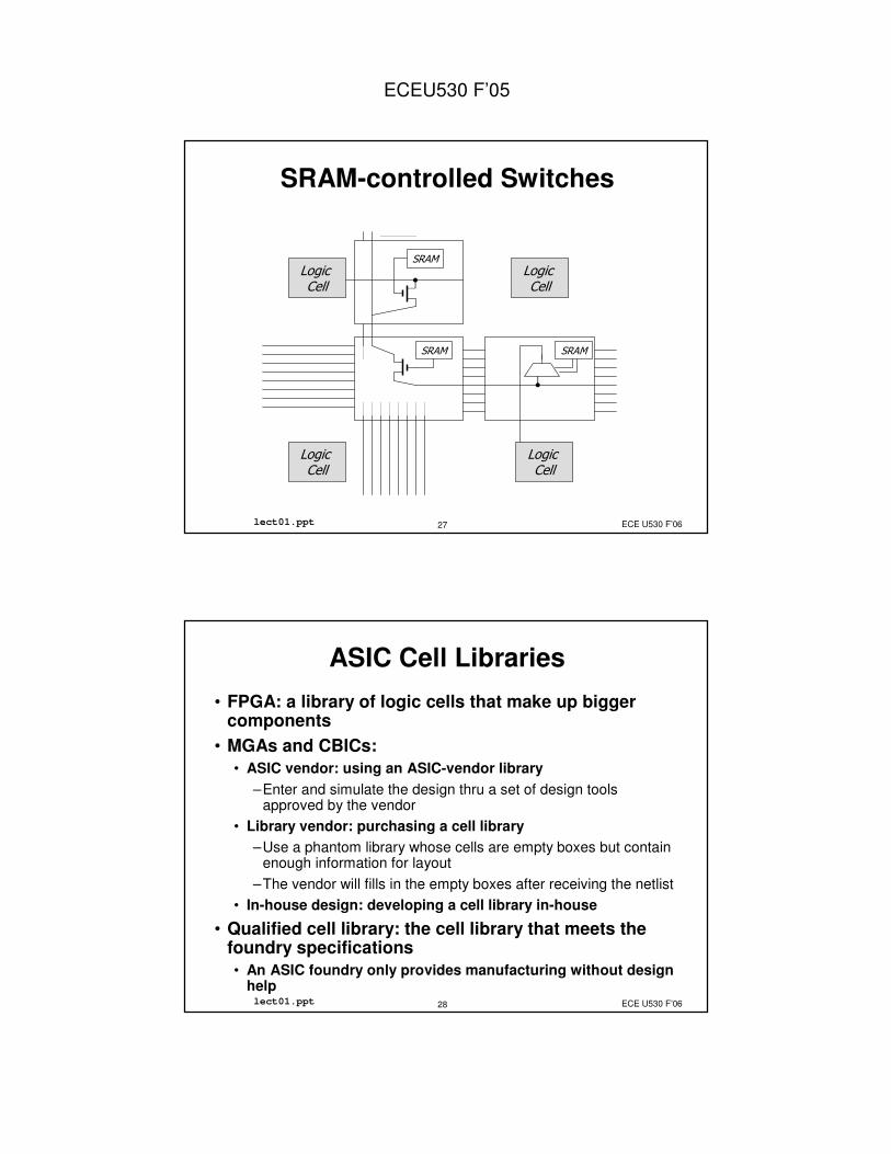
SRAM-controlled Switches
�#�'
�#�' �#�'
�� ��( ��
�� ��( ��
�� ��( ��
�� ��( ��
ECE U530 F’0628lect01.ppt
ASIC Cell Libraries• FPGA: a library of logic cells that make up bigger
components• MGAs and CBICs:
• ASIC vendor: using an ASIC-vendor library–Enter and simulate the design thru a set of design tools
approved by the vendor• Library vendor: purchasing a cell library
–Use a phantom library whose cells are empty boxes but contain enough information for layout
–The vendor will fills in the empty boxes after receiving the netlist• In-house design: developing a cell library in-house
• Qualified cell library: the cell library that meets the foundry specifications• An ASIC foundry only provides manufacturing without design
help
ECEU530 F’05
ECE U530 F’0629lect01.ppt
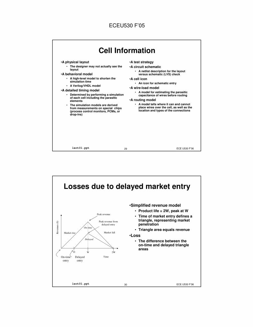
Cell Information•A physical layout
• The designer may not actually see the layout
•A behavioral model• A high-level model to shorten the
simulation time• A Verilog/VHDL model
•A detailed timing model• Determined by performing a simulation
of each cell including the parasitic elements
• The simulation models are derived from measurements on special chips (process control monitors, PCMs, or drop-ins)
•A test strategy•A circuit schematic
• A netlist description for the layout versus schematic (LVS) check
•A cell icon• An icon for schematic entry
•A wire-load model• A model for estimating the parasitic
capacitance of wires before routing
•A routing model• A model tells where it can and cannot
place wires over the cell, as well as the location and types of the connections
ECE U530 F’0630lect01.ppt
Losses due to delayed market entry
•Simplified revenue model• Product life = 2W, peak at W• Time of market entry defines a
triangle, representing market penetration
• Triangle area equals revenue
•Loss • The difference between the
on-time and delayed triangle areas
On-time Delayedentry entry
Peak revenue
Peak revenue from delayed entry
Market rise Market fall
W 2W
Time
D
On-time
Delayed
Rev
enue
s ($
)
ECEU530 F’05
ECE U530 F’0631lect01.ppt
0
200
400
600
800
1000
1200
1400
Exploding: Cost of IC Mask Set
Process (µµµµ) 2.0 … 0.8 0.6 0.35 0.25 0.180.15
0.13
Single Mask cost ($K)
1.5 1.5 2.5 4.5 7.5 1222
40
# of Masks 12 12 12 16 20 2628
30
Mask Set cost ($K)
18 18 30 72 150 312616
1,200
ECE U530 F’0632lect01.ppt
Cost of an ASIC• Quote from
“Spending on masks can pay off, Sematech finds”By David LammersEE Times, July 30, 2003
• A mask set for 130-nm logic devices costs $750,000, on average. Saying that "we think we have a decent handle on mask cost projections," Trybula said that Sematech expects the price tag to rise to $1.6 million for 90-nm technology and $3 million for a 65-nm mask set. "The price goes up very significantly" after that, Trybula said.
ECEU530 F’05
ECE U530 F’0633lect01.ppt
Why FPGAs ?• FPGAs allow you to take advantage of latest
technology • FPGAs are high volume, custom designs • FPGA manufacturers pay the high cost of a mask set
• sell same chip to thousands of customers
• Disadvantages• Designs mapped on FPGAs are slower, larger, dissipate more
power than designs implemented on ASICs• Disadvantages amount to sticking with one or two previous
generations of ASIC chip
• Advantages• No NRE (Non-recurring Engineering cost) for an FPGA• Fast time to market• FPGA CAD tools are cheaper than ASIC CAD tools
ECE U530 F’0634lect01.ppt
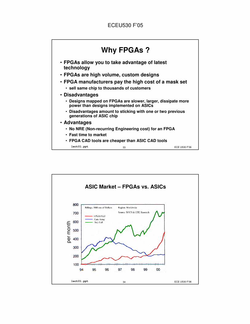
ASIC Market – FPGAs vs. ASICs
per m
onth
ECEU530 F’05
ECE U530 F’0635lect01.ppt
When to use FPGAs?
• Replace components on a board• easier to integrate a single chip
• Replace an ASIC• ASICs getting expensive to fabricate• FPGAs getting denser
• Accelerate algorithms that run in software• for embedded systems• but PCs are getting faster all the time ...
–factor of 2 speed increase in PC parallels afactor of 4 speedup in an FPGA: 2xclock + 2x area
• Goals: • High performance design• Fast design turn around
ECE U530 F’0636lect01.ppt
Classification of Digital Hardware• Chips can be:
• Gate Array or Custom
• Programmable Logic can be:• Mask Programmable (Program once, in the foundary)• Field Programmable (Program anywhere)
• Field Programmable Logic can be:• Program once• Reprogrammable
• Reprogrammable Logic can be:• Reprogrammable out of the circuit (EEPROM based)• Reprogrammable in the circuit
–Reconfigurable Logic is Reprogrammable in the circuit
ECEU530 F’05
ECE U530 F’0637lect01.ppt
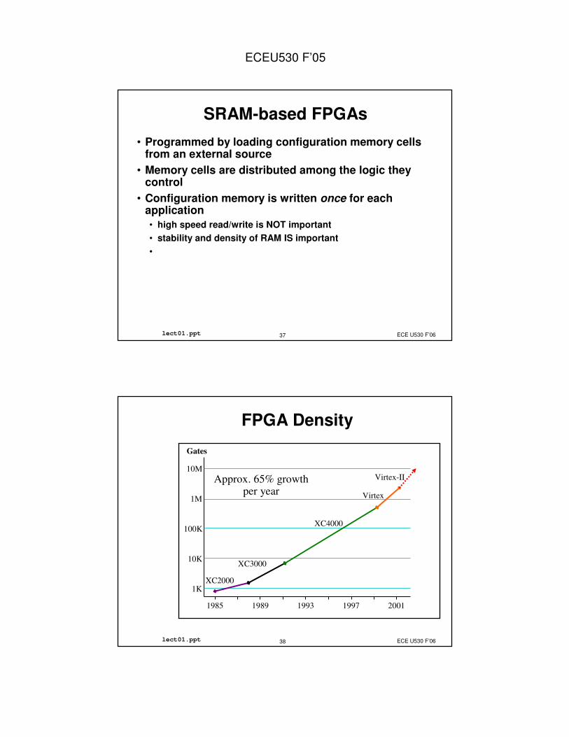
SRAM-based FPGAs• Programmed by loading configuration memory cells
from an external source• Memory cells are distributed among the logic they
control• Configuration memory is written once for each
application• high speed read/write is NOT important• stability and density of RAM IS important•
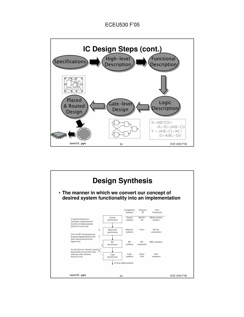
Libraries/IP: Incorporates pre-designed implementation from lower abstraction level into higher level.
Systemspecification
Behavioralspecification
RTspecification
Logicspecification
To final implementation
Compilation/Synthesis:Automates exploration and insertion of implementation details for lower level.
Test/Verification: Ensures correct functionality at each level, thus reducing costly iterations between levels.
Compilation/Synthesis
Libraries/IP
Test/Verification
Systemsynthesis
Behaviorsynthesis
RTsynthesis
Logicsynthesis
Hw/Sw/OS
Cores
RTcomponents
Gates/Cells
Model simulat./checkers
Hw-Swcosimulators
HDL simulators
Gatesimulators
Design Synthesis• The manner in which we convert our concept of
desired system functionality into an implementation
ECEU530 F’05
ECE U530 F’0655lect01.ppt
Design Methodology• Specification• Design domains - abstraction level• Top-down vs. Bottom-up design• Schematic based vs. HDL based• Getting it right – Simulation and verification• Design libraries
ECE U530 F’0656lect01.ppt
Specification• A specification of what to construct is the first major
step.• Compromise between what is wanted and what can
be made• Requires experience
• Requirements must be considered at many levels• System, sub-system, Board
• Specifications can be verified by system simulations
ECEU530 F’05
ECE U530 F’0657lect01.ppt
Design domains
Structural Behavioral
Geometric
Processor, memory
ALU, registersCell
Device, gate
Transistor
Program
State machineModule
Boolean equationTransfer function
IC
Macro
Functional unit
Gate
Masks
Gajski chart
ECE U530 F’0658lect01.ppt
Design Domains (2)• Behavioral:
• Abstract function
• Structural:• Interconnection of parts
• Geometric:• physical objects with sizes and position
ECEU530 F’05
ECE U530 F’0659lect01.ppt
Abstraction levels and synthesis
Architectural level Logic level Circuit level
Beh
avio
ral l
evel
Stru
ctur
al le
vel
For I=0 to I=15Sum = Sum + array[I]
0
0 0
0
State
Memory
+
Control
Clk
Architecturesynthesis
Logicsynthesis
Circuitsynthesis
Layout level
Layoutsynthesis
Ideal synthesis system
(Library)(register level)
ECE U530 F’0660lect01.ppt
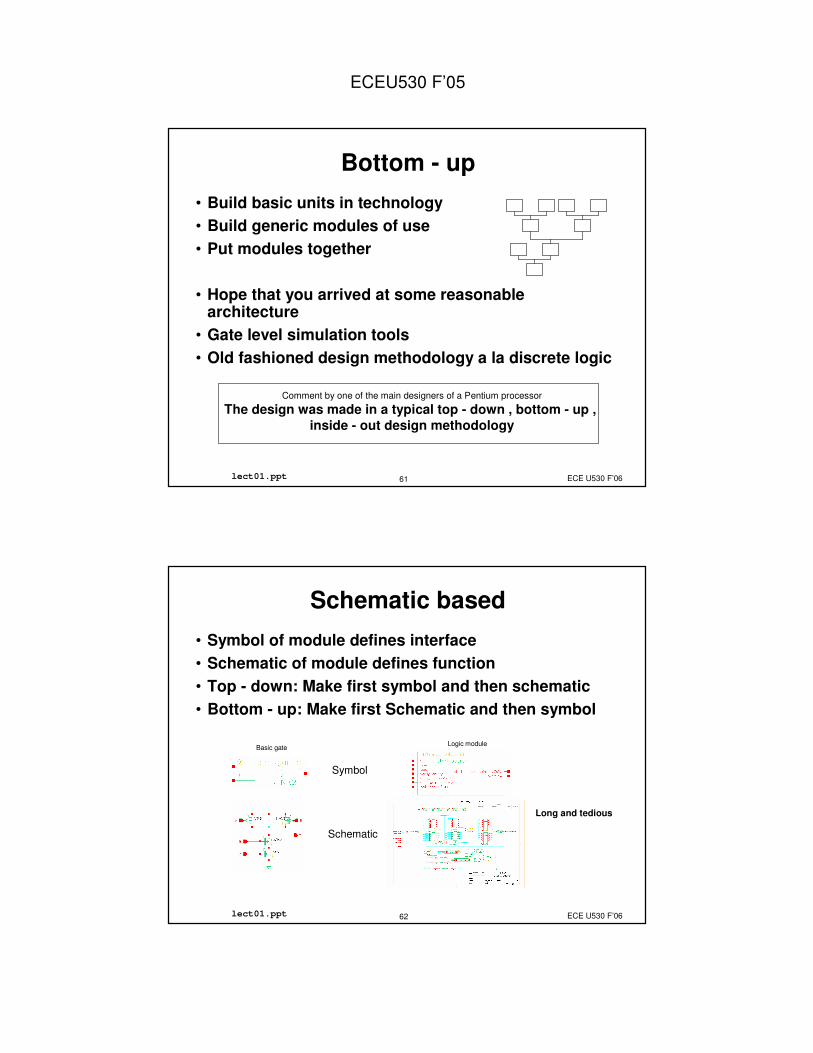
• Choice of algorithm• Definition of functional modules• Definition of design hierarchy• Split up in small boxes - split up in small boxes - split
up in small boxes • Define required units ( adders, state machine, etc.)• Floor-planning• Map into chosen technology
Comment by one of the main designers of a Pentium processor
The design was made in a typical top - down , bottom - up , inside - out design methodology
Bottom - up• Build basic units in technology• Build generic modules of use• Put modules together
• Hope that you arrived at some reasonable architecture
• Gate level simulation tools• Old fashioned design methodology a la discrete logic
ECE U530 F’0662lect01.ppt
Symbol
Schematic
Basic gate Logic module
Long and tedious
Schematic based• Symbol of module defines interface• Schematic of module defines function• Top - down: Make first symbol and then schematic• Bottom - up: Make first Schematic and then symbol