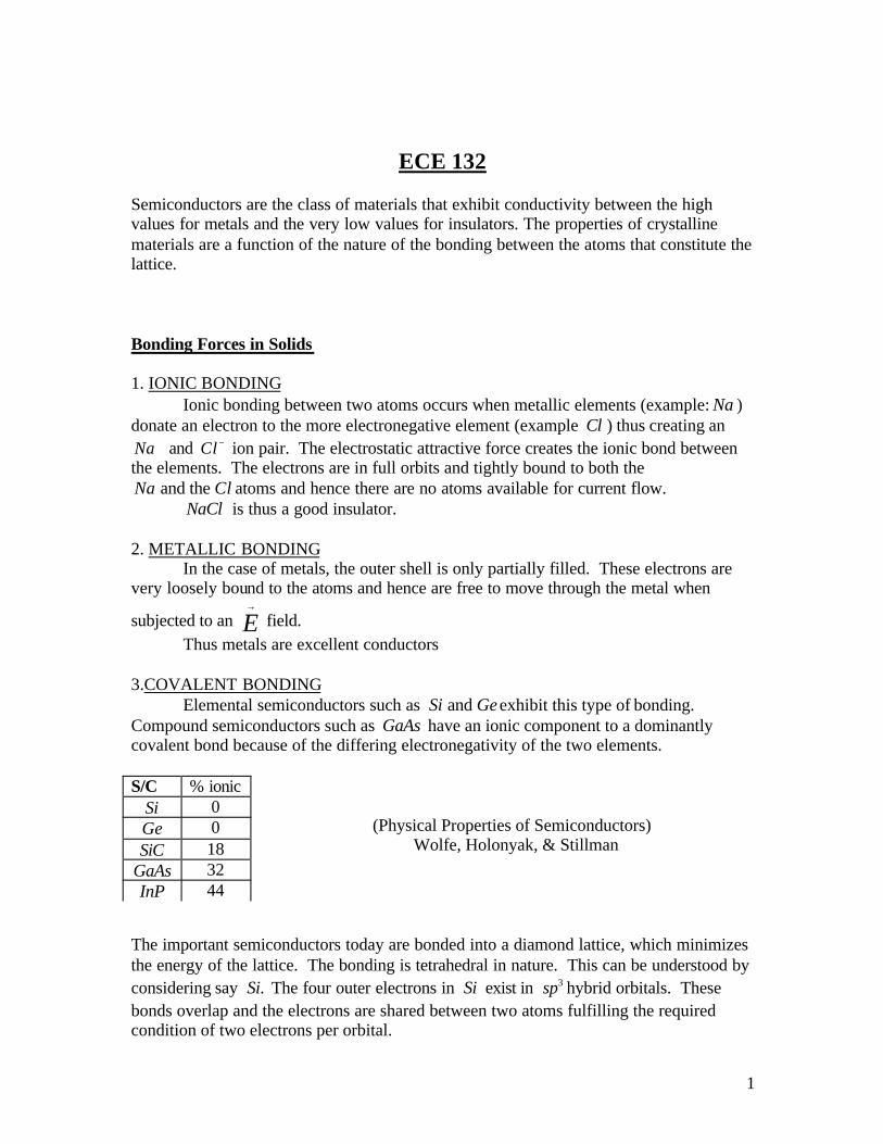
1 ECE 132 Semiconductors are the class of materials that exhibit conductivity between the high values for metals and the very low values for insulators. The properties of crystalline materials are a function of the nature of the bonding between the atoms that constitute the lattice. Bonding Forces in Solids 1. IONIC BONDING Ionic bonding between two atoms occurs when metallic elements (example: Na ) donate an electron to the more electronegative element (example Cl ) thus creating an Na and Cl - ion pair. The electrostatic attractive force creates the ionic bond between the elements. The electrons are in full orbits and tightly bound to both the and the Na Cl atoms and hence there are no atoms available for current flow. NaCl is thus a good insulator. 2. METALLIC BONDING In the case of metals, the outer shell is only partially filled. These electrons are very loosely bound to the atoms and hence are free to move through the metal when subjected to an E → field. Thus metals are excellent conductors 3.COVALENT BONDING Elemental semiconductors such as and Si Ge exhibit this type of bonding. Compound semiconductors such as GaAs have an ionic component to a dominantly covalent bond because of the differing electronegativity of the two elements. (Physical Properties of Semiconductors) Wolfe, Holonyak, & Stillman The important semiconductors today are bonded into a diamond lattice, which minimizes the energy of the lattice. The bonding is tetrahedral in nature. This can be understood by considering say . Si The four outer electrons in Si exist in 3 sp hybrid orbitals. These bonds overlap and the electrons are shared between two atoms fulfilling the required condition of two electrons per orbital. S/C % ionic Si 0 Ge 0 SiC 18 GaAs 32 InP 44
Transcript
1
ECE 132
Semiconductors are the class of materials that exhibit conductivity between the high values for metals and the very low values for insulators. The properties of crystalline materials are a function of the nature of the bonding between the atoms that constitute the lattice. Bonding Forces in Solids 1. IONIC BONDING
Ionic bonding between two atoms occurs when metallic elements (example: Na ) donate an electron to the more electronegative element (example Cl ) thus creating an Na+ and Cl − ion pair. The electrostatic attractive force creates the ionic bond between the elements. The electrons are in full orbits and tightly bound to both the
and the Na Cl atoms and hence there are no atoms available for current flow. NaCl is thus a good insulator.
2. METALLIC BONDING In the case of metals, the outer shell is only partially filled. These electrons are very loosely bound to the atoms and hence are free to move through the metal when
subjected to an E→
field. Thus metals are excellent conductors
3.COVALENT BONDING Elemental semiconductors such as and Si Geexhibit this type of bonding. Compound semiconductors such as GaAs have an ionic component to a dominantly covalent bond because of the differing electronegativity of the two elements.
(Physical Properties of Semiconductors) Wolfe, Holonyak, & Stillman
The important semiconductors today are bonded into a diamond lattice, which minimizes the energy of the lattice. The bonding is tetrahedral in nature. This can be understood by considering say .Si The four outer electrons in Si exist in 3sp hybrid orbitals. These bonds overlap and the electrons are shared between two atoms fulfilling the required condition of two electrons per orbital.
S/C % ionic Si 0 Ge 0 SiC 18
GaAs 32 InP 44
2
Ionic Bonding
Metallic Bonding
Covalent Bonding
+
+
+ +
⇒ Na Na Na
_
_ _
_
Si
Si Si
Si Si Si
SiSi
3sp
3sp3sp
=
+
Cl Na Cl Na
3
Another Pictorial Representation
The energy levels of a hydrogen atom is obtained as
4 2
2 2 2
13.62
rn
m e z eVE
n n= − = −h
This is obtained by solving the Schrödinger equation for a coulombic potential.
Solid
Next band is empty (conduction band)
Last-filled band (valence band)
Full of electrons
+Z z is the atomic number
Single atom
2
( ) Ze
V rr
−=
Energy levels, nE
4
Note that the energy gaps between the quantized energy levels in a single atom are the origin of the band gap for solids. Typical numbers for band gap for various solids: This is the MINIMUM energy required to allow an electron to leave the (mostly) full valence band and occupy a state in the conduction band. An analogy is say a football stadium.
The step height is analogous to the band gap in that an energy difference less than the step height will not get you to the next step. The energy required to move an electron from the valence band (VB) to the conduction band (CB) is related to the bond strength and can be provided by one of several means; thermal, light (photons), high energy particles, etc. Thermal energy exists in each solid at temperatures T>OK. A measure of thermal energy is Bk T where Bk is the Boltzmann’s constant and 25 9 Bk T meV⋅∼ at room temperature (300K by convention). 1 eV = Energy required to move one electron up a potential energy of 191 1 6 x 10V −= ⋅ coulombs 191 1 6 x 10V −= ⋅ Joules.
Semiconductor
1 1 1 4 0 7
gE
Si eVGaAs eV
Ge eV
⋅⋅⋅
2 9 0
3 4
SiO eV
GaN eV
⋅
⋅
cE
vE1 1 eV⋅
iS
cE
vEGaAs
1 4 eV⋅
cE
vEGaN
3 4 eV⋅
cE
vE
9 0 eV⋅
2SiO
Field
Step height ∼ Band gap
SEATS
5
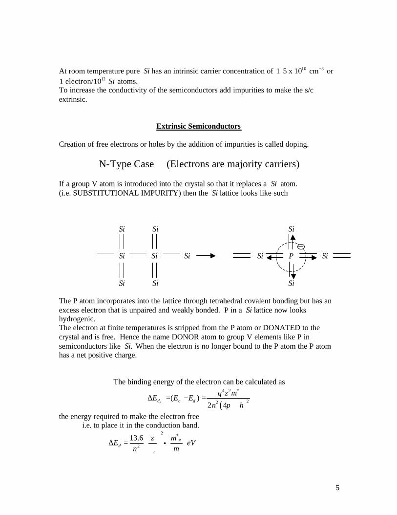
At room temperature pure Si has an intrinsic carrier concentration of 10 31 5 x 10 cm or−⋅
121 electron/10 atoms.Si To increase the conductivity of the semiconductors add impurities to make the s/c extrinsic.
Extrinsic Semiconductors Creation of free electrons or holes by the addition of impurities is called doping.
N-Type Case (Electrons are majority carriers) If a group V atom is introduced into the crystal so that it replaces a Si atom. (i.e. SUBSTITUTIONAL IMPURITY) then the Si lattice looks like such Si Si Si Si Si Si P Si Si Si Si The P atom incorporates into the lattice through tetrahedral covalent bonding but has an excess electron that is unpaired and weakly bonded. P in a Si lattice now looks hydrogenic. The electron at finite temperatures is stripped from the P atom or DONATED to the crystal and is free. Hence the name DONOR atom to group V elements like P in semiconductors like .Si When the electron is no longer bound to the P atom the P atom has a net positive charge.
The binding energy of the electron can be calculated as
( )
4 2
22( )
2 4nd c dq z m
E E En hπ
∗
∆ = − =∈
the energy required to make the electron free i.e. to place it in the conduction band.
2
2
13.6 ed
r
z mE eV
n m
∗ ∆ = ∈
i
Si
6
Recall: 2
13.6nE
n= for a hydrogen atom
cE dE aE∆ aE vE
Intrinsic Semiconductor As stated previously an intrinsic semiconductor has no free carriers at 0K and hence is then an insulator. At any finite temperature, however, the covalent bonds break producing electron-hole pairs. ∴At steady state
Intrinsic carrier concentrationin p n≡ ≡ ← Since the electrons can be recaptured by the orbital lacking an electron, this is referred to as to RECOMBINE WITH A HOLE. At steady state At all temperatures
i ir g≡
↗ ↖
Recombination rate Generation rate
As : i iT g r↑ ↑⇒ ↑
3 1mEHPc s− −
At all temperatures
7
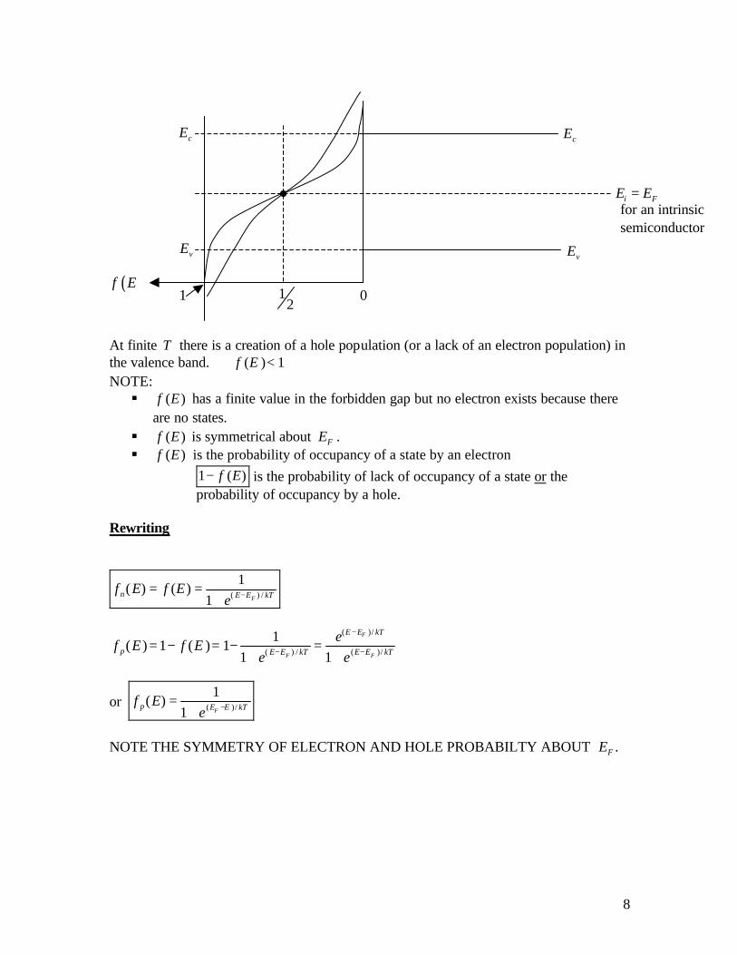
As iEg n↑ ↓ (1.1 ) eV Si 10 31.45 x 10 cm− Eg (1.4 ) GeV aAs 6 31.79 x 10 cm− Study the nature of ( )f E At 0T K=
( )( 0)f E T = = 1 for 0 for
F
F
E EE E
<>
It is impossible for electrons to occupy energy above FE at 0T K= At finite T
( )f E is the probability of occupancy of an AVAILABLE STATE. ∴ if no state exists and even is ( ) 1f E = there will be no electron at that energy. In a semiconductor
5
23
8 62 x 10
138 x 10
eVk
B
Jk
k−
−
=
=
ii
@ 300 26Bk T T K meV= =
11
12
1
1 2
d dd F
aa F
N NE E
ekT
Na NE E
ekT
+
−
=− +
=−
+
0T =
1 0T >
2 1T T>
FE
8
At finite T there is a creation of a hole population (or a lack of an electron population) in the valence band. ∴ ( ) 1f E < NOTE: § ( )f E has a finite value in the forbidden gap but no electron exists because there
are no states. § ( )f E is symmetrical about FE . § ( ) is the probability of occupancy of a state by an electronf E
1 ( )f E− is the probability of lack of occupancy of a state or the probability of occupancy by a hole.
Rewriting
( ) /
1( ) ( )
1 Fn E E kTf E f Ee −= =
+
( )/
( ) / ( )/
1( ) 1 ( ) 1
1 1
F
F F
E E kT
p E E kT E E kT
ef E f E
e e
−
− −= − = − =+ +
or ( )/
1( )
1 Fp E E kTf Ee −=
+
NOTE THE SYMMETRY OF ELECTRON AND HOLE PROBABILTY ABOUT .FE
vE
i FE E= for an intrinsic semiconductor
cE
12
0
vE
cE
( )f E1
9
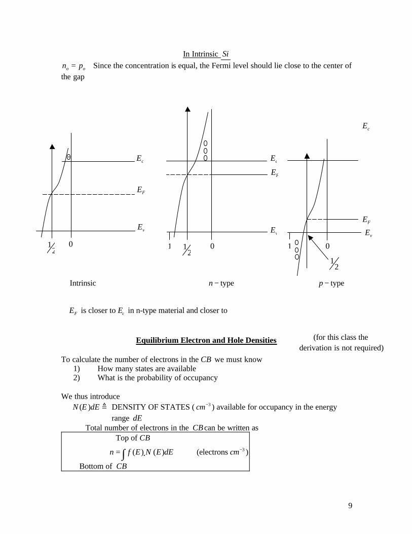
In Intrinsic Si
o on p= Since the concentration is equal, the Fermi level should lie close to the center of the gap
is closer to in n-type material and closer toF cE E∴
Equilibrium Electron and Hole Densities To calculate the number of electrons in the CB we must know
1) How many states are available 2) What is the probability of occupancy
We thus introduce ( )N E dE @ DENSITY OF STATES ( 3cm− ) available for occupancy in the energy range dE
∴ Total number of electrons in the CB can be written as
3
Top of
( ) ( ) (electrons )
Bottom of
CB
n f E N E dE cm
CB
−= ∫ i
cE
(for this class the derivation is not required)
12
0
cE
FE
vE
0
12
1
cE
FE
vE
FE
vE
0
12
1
Intrinsic typen − typep −
10
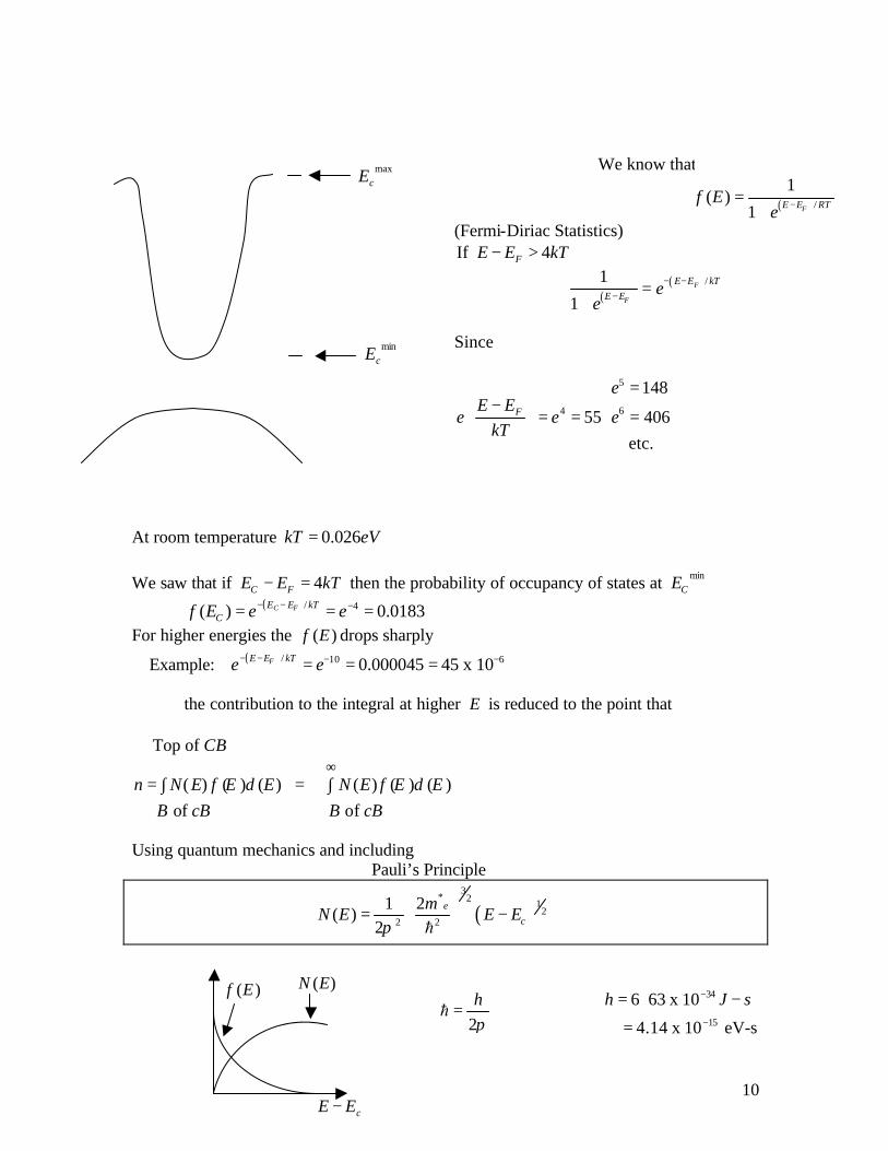
At room temperature 0.026kT eV= We saw that if 4C FE E kT− = then the probability of occupancy of states at min
CE
( ) / 4( ) 0.0183C FE E kTCf E e e− − −= = =
For higher energies the ( )f E drops sharply
Example: ( ) / 10 60.000045 45 x 10FE E kTe e− − − −= = =
∴ the contribution to the integral at higher E is reduced to the point that Top of
( ) ( ) ( ) = ( ) ( ) ( ) of of
CB
n N E f E d E N E f E d EB cB B cB
∞= ∫ ∫
Using quantum mechanics and including Pauli’s Principle
( )3
2 12
2 2
1 2( )
2e
cm
N E E Eπ
∗ = −
h
2hπ
=h 34
15
6 63 x 10
4.14 x 10 eV-s
h J s−
−
= ⋅ −
=
( )N E ( )f E
cE E−
maxcE
mincE
We know that
( ) /
1( )
1 FE E RTf Ee −=
+(Fermi-Diriac Statistics) If 4FE E kT− >
( )( ) /1
1F
F
E E kTE E e
e− −
− =+
Since
5
4 6
148
55 406 etc.
F
eE E
e e ekT
= − = = =
11
Here em∗ is the density of state effective mass
( ) ( )3
2 1 /22 2
1 22
F
c
e E E kTc
E
mn E E e dE
π
∞ ∗− −
= −
∫ i i ih
Multiplying and dividing by
( )3
2 we getkT=
( ) ( )
3 12 2/
2 2
1 22
FE E kTe cE Em dEn e
kTkTπ
∗− − −
=
∫i i i ih
Define cE Eu
kT− @
( )3 12 2
2 2/1 2
2
ccFe c c
E EE E kT kT E E E Em kT
n e e dkT kTπ
∗
−−− − − ∴ = ∫
i i ih
( )3
2 12
2 20
/1 2
2cFe u duE E kTm kT
n e e uπ
∗−−
∞ ∴ =
∫i ih
1
2
0
(From definite integral tables)2
ue u duπ∞
− =∫ i
( )3
2
2
/22 cFe E E kTm kT
n eπ ∗
− =
i ih or ( ) / c FE E kT
cn N e− −=
3
2
2
22 Effective density of states in the e
cm kT
N CBh
π ∗ =
@
i.e. Instead of considering the occupancy by electrons of all the states from min
cE to
max, c cE N gives us the number of electrons in the CB by considering all the states in the band to be effectively at the band edge populated with a probability
function ( ) / .c FE E kTe− − Likewise, proceeding in a similar manner for the holes in the VB we obtain
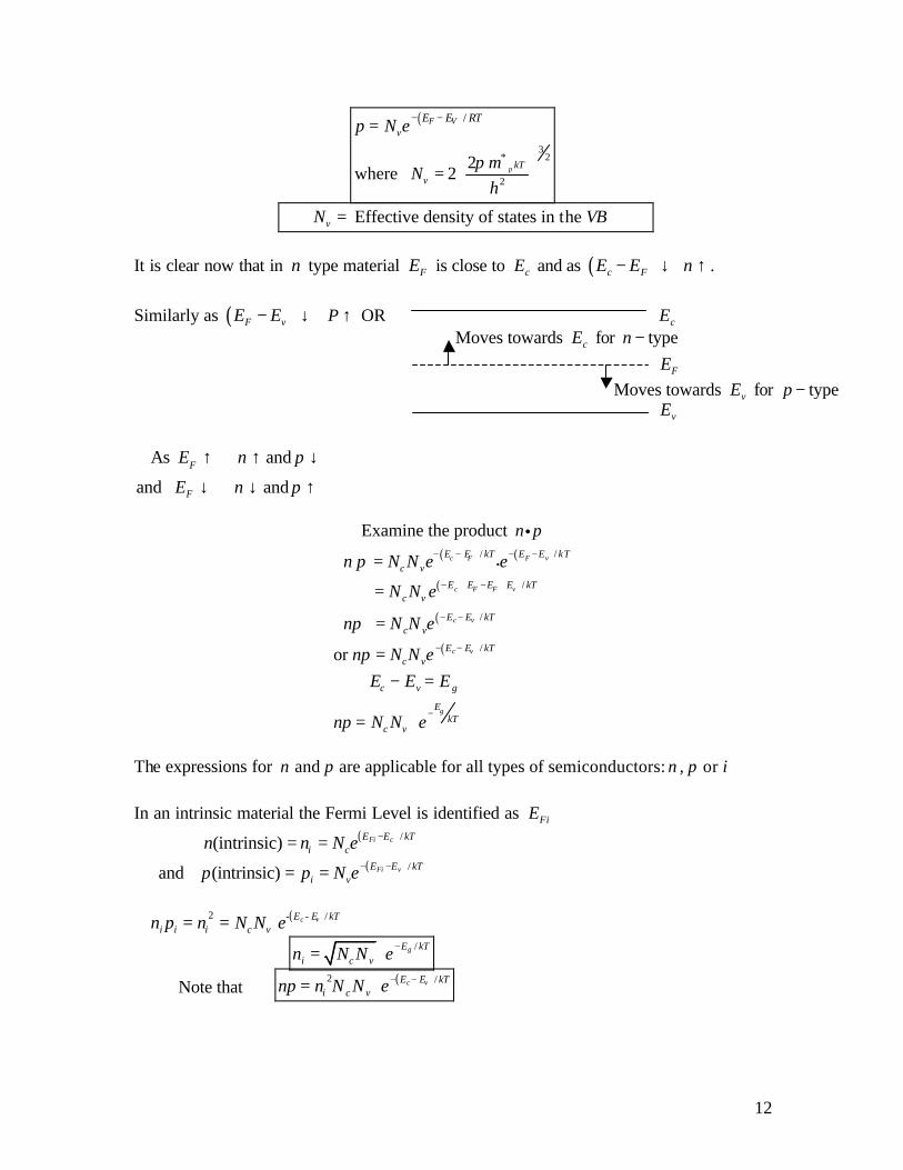
12
( )
32
2
/
2where 2 p
F Vv
kTv
E E RTp N e
mN
hπ ∗
− −=
=
Effective density of states in the vN VB= It is clear now that in n type material FE is close to cE and as ( ) c FE E n− ↓ ↑ . Similarly as ( )F vE E− P↓ ↑ OR cE FE vE As and
and and F
F
E n p
E n p
↑ ↑ ↓
↓ ↓ ↑
Examine the product n pi
( ) ( )
( )
( )
( )
/ /
/
/
/
or
c F F v
c F F v
c v
c v
g
E E kT E E kTc v
E E E E kTc v
E E kTc v
E E kTc v
c v g
EkT
c v
n p N N e e
N N e
np N N e
np N N eE E E
np N N e
− − − −⋅ ⋅
− + − +⋅
− −
− −
−
=
=
=
=− =
=
i
The expressions for and are applicable for all types of semiconductors: , or n p n p i In an intrinsic material the Fermi Level is identified as FiE
( ) / (intrinsic) Fi cE E kTi cn n N e −= =
( ) /and (intrinsic) Fi vE E kTi vp p N e− −= =
( )2 - - / c vE E kT
i i i c vn p n N N e∴ = =
/ gE kT
i c vn N N e−=
Note that ( )2 / c vE E kTi c vnp n N N e− −=
Moves towards cE for typen −
Moves towards vE for typep −
13
Now that we can relate FE to the nature of the and CB VB through and n pm m∗ ∗ we can recalculate, ,
iFE more accurately. Any asymmetry in &n p distribution has to be introduced through differences in & c vN N .
( ) / 2 c FiEg
E E kT kTi c c vn N e N N e
−− −= =
( ) / 2 c F iEg
E E kT v kT
c
Ne e
N−− −⇒ =
exp exp2
exp /2
c Fi v
c
vc Fi
c
E E NEgkT kT N
NEgE E kT
N
− +∴ • =
⇒ − + + =
Taking ln of both sides
ln2
vc Fi
c
NEgE E kT
N− + + =
Since g c vE E E= −
ln2 2
c v vFi c
c
E E NE E kT
N= − − +
∴ v
c
N1 ln
2 2 Nc v
Fi
E EE kT
+= +
The second turn is the derivation of
iFE from the middle of the gap.
12 0
cE
FE
vE
14
So what is the dependence of vs ?n T
Space Charge Neutrality We can dope a semiconductor with both donors and acceptors Donate electrons ↵ ↘Accept electrons i.e. remove electrons
effective
effective
for n-type material for p-type
d A
a d
n N Np N N
≅ −≅ −
These materials are called compensated semiconductors.
( )
( )
/
/
and
c F
F v
E E kTc
E E kTv
n N e
p N e
− −
− −
=
=
In a bulk semiconductor there must be charge neutrality everywhere because any excess charge will immediately set up an electric field.
Low temp
1710
1510
1310
High temp
1000/T
n Nd Nd+≅ <
Intrinsic
Freeze-out Extrinsic region
are still valid relations.
15
Q
E F qe E
→
= = −
The electrons will flow towards the positive charge until the value is reduced to 0.Q Then 0. The attractive force, 0.E F→ ⇒ →
o D op N n N A
−++ = + Bulk semiconductor at equilibrium
o D A on N N p−
+ = − +
iE
Conductivity and Mobility
+
+
+
+ ++
++
QE
F qE= −
o D An N N+ −−; or neglecting op
Ed
Ea
FE
16
At any temperature the individual electrons show randomized motion. Scattering with the lattice is the dominant randomizing process. If we apply a field, xE then
/per electron xF qE= −
∴ Net change of momentum of the electron ensemble=
3 where # of electrons/cm
xdp
nqEdt
n
= −
=
We want to use this equation to determine the response of an electron to an applied electric field. i.e. The relationship between its velocity and the applied field. Assume:
1) The probability of collision is constant 2) # of electons in the group at 0oN t= = 3) ( ) # of electrons which have not undergone collisions by time N t t=
Let the scattering rate or number of collisions/sec be K .
∴ The rate of decrease of ( ) ,N t the scattered population is given by
( ) ( ) (assumption #1)
( ) ln ( )
( )
dN tKN t
dtdN t
Kdt N t Kt cN t
= −
∴ = − ⇒ = − +
Since ( )0 , lno oN t N c N= = =
∴ ( ) KtoN t N e−=
t−
17
Let t− be the mean time between collisions
( )
( )
Kto
Kto
N te dtt N t dtt
N t dt N e dt
−−
−
∞∞
∞ ∞=∫∫
∫ ∫oo
o o@ so 1 t K
−= and ( )
tt
oN t N e−
=
The probability that an electron will experience a collision in an interval dt is .dt
t− This
is equivalently the fraction of electrons that undergo a collision. Let xp be the momentum in the direction.x −
because momemtum decreases
x xdt
dp pt−∴ = −
↑
or rate of decrease of due to collisionsx xx
dp pp
dt t−
−=
rate of increase of due to xx x x
dpqnE p E
dt= −
At steady state rate of momentum increase due to xE = rate of momentum decrease due to collision.
, the average momentum/electron
xx x x
xx x
PqnE P n q t E
tP
P q t En
−
−
−
∴ = − ⇒ = −
∴< > = −@
x xx
n n
P q t EV
m m
−
∗ ∗
< > −∴ < >= =
Introduce the concept of mobility
2 1 1 nx n n x
n
q tV E cm V s
mµ µ
−
− −∗< > = − ⇒ =
px p xp
p
qtV E
mµ µ
−
∗= ⇒ =
18
x nV< > is the net drift of the electron distribution under the influence of xE . The current density resulting from the drift velocity is
nx x n
px x p
J qn V
J qp V
= − < >
= + < >
2
.nx xn n
q t q ntJ qn E E
m m
− −
∗ ∗
− + ∴ = − =
Rewriting as conventional Ohm’s Law
2
Note :
nx n x nn
n n p p
nq tJ E
m
qn qp
σ σ
σ µ σ µ
−
∗=
= =
@
If both electrons and holes are present
( )x px nx n p xJ J J q n p Eµ µ= + = +
Since the probabilities of scattering add 1 2K K K= +
1 1
Since ii
K
itα
µ−= 1 2
1 1 1µ µ µ
= + Matthiesen’s Rule
Measurement of Semiconductor Parameters 1) Effective mass m∗ can be determined by electron resonance. Under a magnetic field the electron motion is circular.
energyRF
Lattice scattering
32T
−32T
Impurity scattering
2
Centripetal force magnetic flux density
mvqvB
r=
↑↗vB
r
19
or c
qBr qBv
m mω∗ ∗∴ = = =
If RF energy is incident on the sample it will be transmitted for all frequencies except
cω when resonance absorption of energy occurs. (Reduced transmission) By measuring cω we can calculate or n pm m∗ ∗ . 2) Mobility (Hall Effect) and Carrier Concentration z y x Consider a p-type bar, which is subject to an electric field xE and a magnetic field zB . The force on a single hole
( )
y y x z
F q E V x B
F q E v B
→ → → = +
∴ = −
yE is the electric field that is set up by the holes that were deflected under the influence
of the force .x zv B Since no current can flow in the y-direction. 0 y y x zF E v B= ⇒ =
The xv can be obtained from xJ as
where hole concentrationxx o
o
Jv p
qp= =
+
Cyclotron resonance frequency
yE
xE
Lw
xI
zB
t
AV
DV
BV
cV
20
xy z H x z
o
JE B R J B
qp∴ = =i
Where 1
Hall CoefficientHo
Rqp
= =
1
x zxx o
H y
x zA B ABy o
AB
J BIJ pwt qR qE
I BV V VE p
w w qtV
= ∴ = =
−= = =
1 /
where /
CD x
o o
V IRwtqp qp L L wtσ
µ = = = =
Excess Carriers in Semiconductors :
The beam is absorbed
( )
( )
( ) xo
dI xI x
dxI x I e α
α
−
− =
⇒ =
absorption coefficient
is the energy of the photon in .
1 24( )
( )eV
hc eVhv E
mλ λ µ⋅
= = =14444244443
hv Eg>
emission of light (direct semiconductor)
generation
Recombination
Eg1( )cmα −
E
21
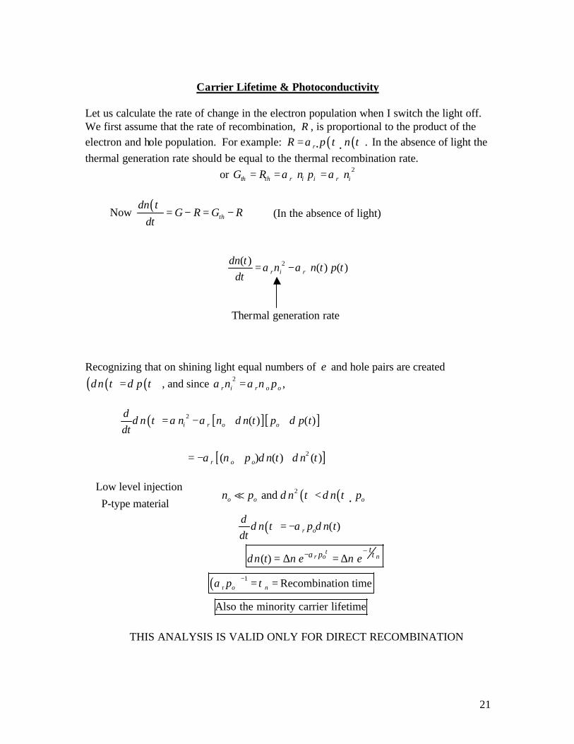
Carrier Lifetime & Photoconductivity
Let us calculate the rate of change in the electron population when I switch the light off. We first assume that the rate of recombination, R , is proportional to the product of the electron and hole population. For example: ( ) ( ) .rR p t n tα= i i In the absence of light the thermal generation rate should be equal to the thermal recombination rate.
or 2 th th r i i r iG R n p nα α⋅ ⋅= = =
Now ( )
th
dn tG R G R
dt= − = −
2( ) ( ) ( )r i r
dn tn n t p t
dtα α= −
Recognizing that on shining light equal numbers of e and hole pairs are created
( ) ( )( )n t p tδ δ= , and since 2r i r o on n pα α ⋅= ,
( ) [ ][ ]2 ( ) ( )i r o o
dn t n n n t p p t
dtδ α α δ δ= − + +
[ ]2( ) ( ) ( )r o on p n t n tα δ δ= − + +
Low level injection P-type material∴
( ) ( )2 and o o on p n t n t pδ δ⇒ < i=
( )
( ) 1r
( )
( )
Recombination time
Also the minority carrier lifetime
r o
o n
tr o n
tp
dn t p n t
dt
n t n e n e
p
α τ
δ α δ
δ
α τ−
−−
⇒ = −
⇒ = ∆ = ∆
= =
THIS ANALYSIS IS VALID ONLY FOR DIRECT RECOMBINATION
Thermal generation rate
(In the absence of light)
22
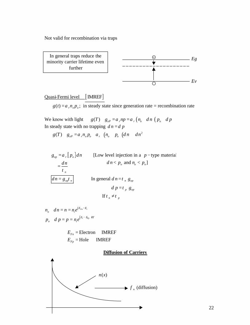
Not valid for recombination via traps
Quasi-Fermi level [ ]IMREF
( ) r o og t n pα= ; in steady state since generation rate = recombination rate We know with light ( )( )( ) oP r r o og T g np n n p pα α δ δ+ = = + + In steady state with no trapping n pδ δ=
( ) ( ) 2( )
oP r o o r o og T g n p n p n nα α δ δ + = + + +
[ ]
In general
If
op r o
n
op n n op
p op
n
g p n
n
n g n g
p g
α δ
δτ
δ τ δ τ
δ τ
τ τ
=
=
⇒ = =
=
≠ p
( )
( )
Fn i
i Fp
E Eo i
E E RTo i
n n n n e
p p p n e
δ
δ
−
−
+ = =
+ = =
Electron IMREFHole IMREF
Fn
Fp
EE
==
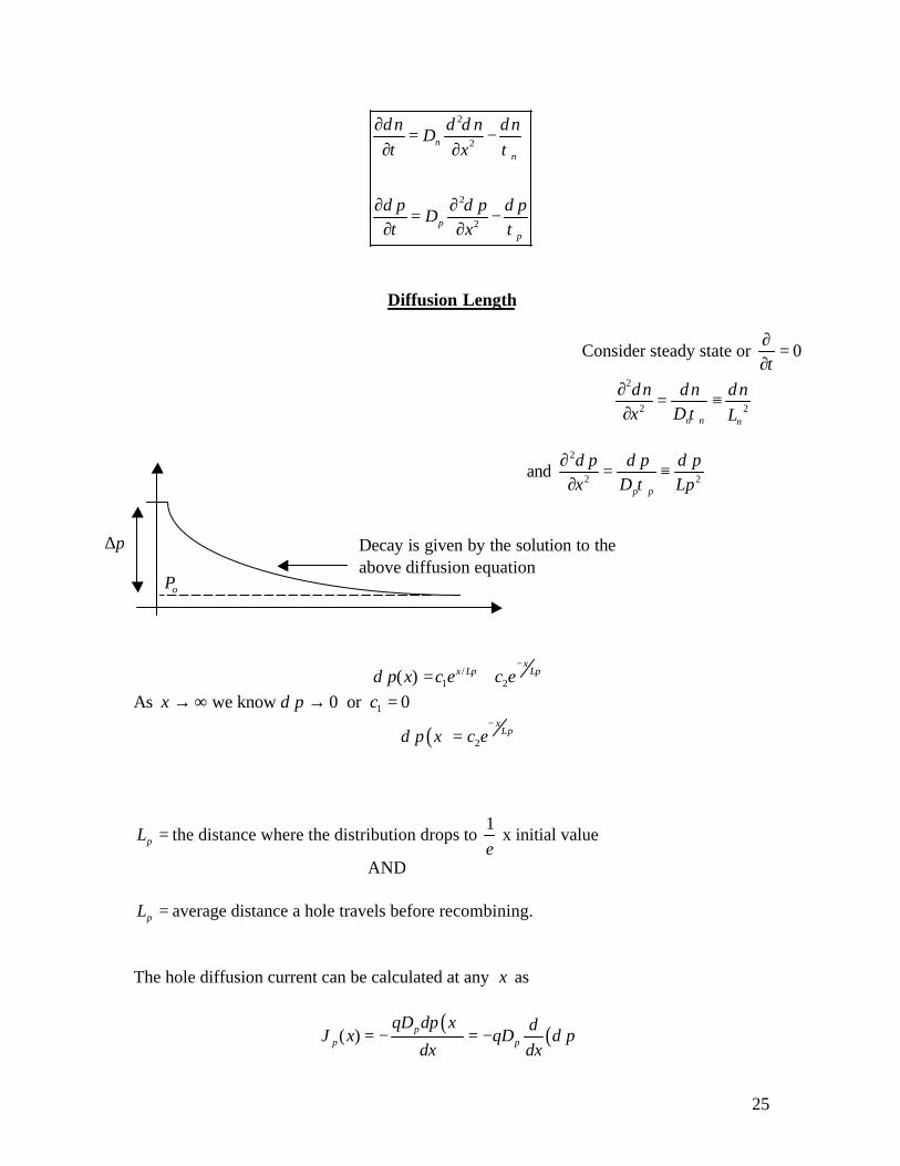
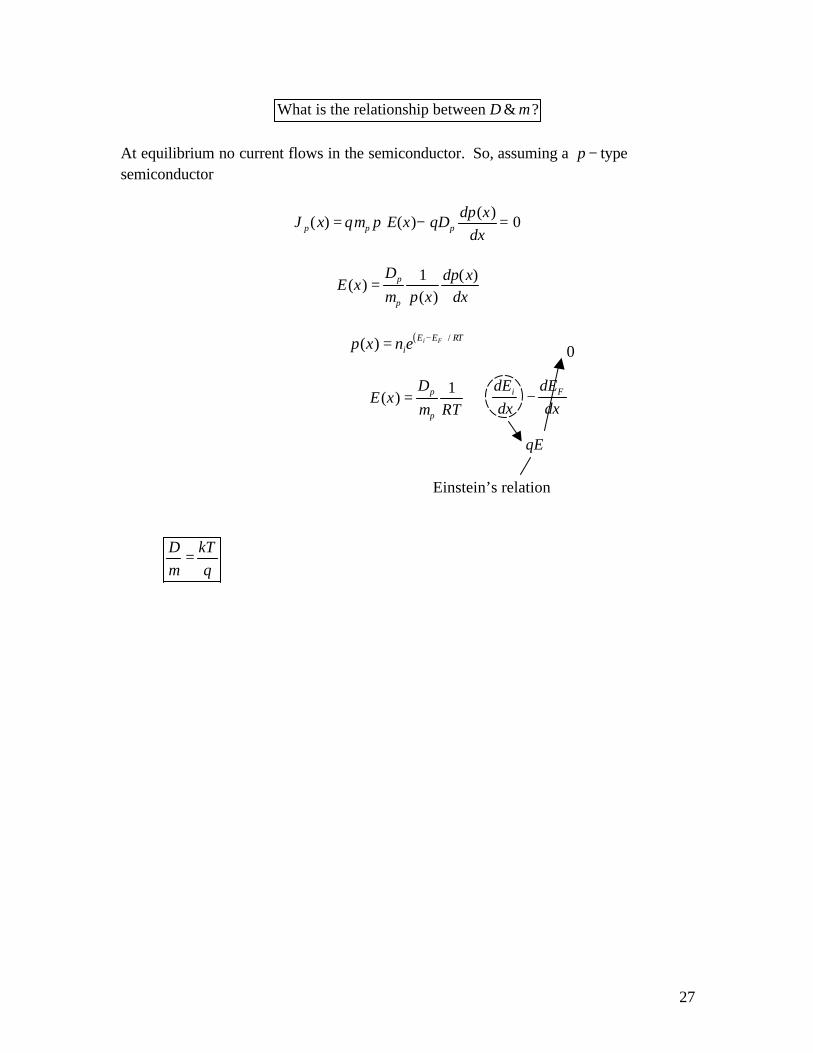
Diffusion of Carriers
Eg
Ev
In general traps reduce the minority carrier lifetime even
further
( )n x
(diffusion)nφ
[Low level injection in a p − type material and ]o o on p n pδ⇒ < <
23
( )
( )
The negative sign represents diffusion from higher to lower concentration
n ndn x
x Ddx
φ = −
↑
( )
( )p p
dp xx D
dxφ = −
The diffusion current ( )
n n
n n
p p
dnJ q D
dx
dnJ qD
dx
dpJ qD
dx
= − −
=
= −
i
In the presence of an electric field
( ) drift diffusion
n n nJ x J J= +
( ) ( )( ) ( )
( )( ) ( ) ( )
n n n
p p p
dn xJ x q n x E x qD
dxdp x
J x q p x E x qDdx
µ
µ
= +
= −
( ) ( ) ( )n pJ x J x J x= +
Continuity Equation
A ( )Jp x x+ ∆ ( )Jp x
x x x+ ∆
x∆
A= Area in 2cm and x∆ is the length of the box in centimeters.
or the total current is the sum of all electron and hole currents
24
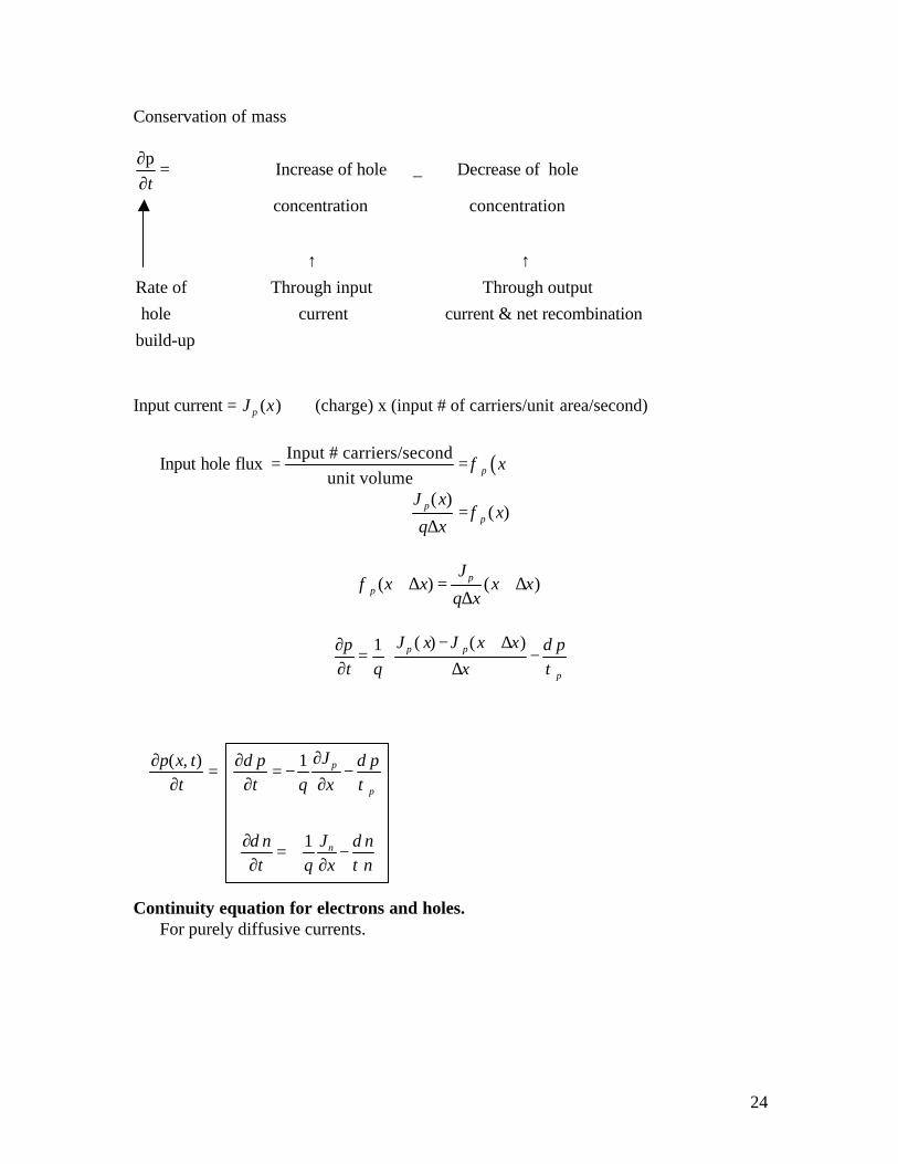
Conservation of mass
p Increase of hole _ Decrease of hole
concentration concentration
t∂
=∂
↑ Rate of Through input Through output hole
↑
current current & net recombinationbuild-up Input current ( ) (charge) x (input # of carriers/unit area/second)pJ x= ⇒


![[h1] Acoustical and Perceptual Dimensions of Soundlocker.wcupa.edu/jazz/classfiles/SoundPrimerfromEMT.pdf · [h1] Acoustical and Perceptual Dimensions of Sound ... or Alison Krause](https://static.documents.pub/doc/80x56/5b6f79fe7f8b9a66338bfd6c/h1-acoustical-and-perceptual-dimensions-of-h1-acoustical-and-perceptual.jpg)

