ECE 526 Digital Integrated Circuit Design with Verilog and SystemVerilog Laboratory Manual Department of Electrical and Computer Engineering California State University, Northridge Fall 2014
Transcript
ECE 526
Digital Integrated Circuit Design with Verilog and
SystemVerilog
Laboratory Manual Department of Electrical and Computer Engineering California State University, Northridge Fall 2014
10. Lab 8. Arithmetic-Logic Unit Modeling………………………………………. 43
11. Lab 9. Modeling a Sequence Controller………………………………………. 45
12. Lab 10. Final Project: The RISC-Y CPU……………………………………. 52
13. Appendix A Unix Command Reference Guide …………….………………... 57
14. Appendix B vi Editor Command Reference Guide …………………………… 61
3
Documentation Guidelines Laboratory Reports All laboratory reports will have a cover page with the students’ names, the class, the problem number and the problem title prominently displayed. All lab reports must include printouts of graphical waveforms showing simulation results and log files of the simulations done. Resolve any errors or warnings before submitting a lab report. Submitted log files may not contain warning or error messages. All text, code and waveforms are to be computer printed without edits. You may copy the file into a word processor adding page breaks, titles and page numbers but nothing more. While these computer-generated outputs and all source code must be included in a lab report, they are supporting documentation, not the body of the lab report. The essential elements of a lab report are:
– A statement of what you are accomplishing, demonstrating, determining, etc.
– Methodology: statement of how you did it. Specifically include a test plan. Include flow charts and other materials as appropriate.
– Analysis of results: what did you demonstrate/prove. – Conclusions.
Any lab report without the above elements will be incomplete and will be graded accordingly. Academic Dishonesty Submitting any report that is not entirely your own work is a form of academic dishonesty and will not be tolerated. Each and every lab report must include the following statement, signed and dated by the student. Lab reports without the statement will be summarily rejected.
I hereby attest that this lab report is entirely my own work. I have not copied either code or text from anyone, nor have I allowed or will I allow anyone to copy my work. Name (printed) _______________________________ Name (signed) _______________________________ Date _________________
4
Documentation This is a course about hardware development using a hardware description language. The application may be modeling hardware but the method is coding of language constructs. As such, documentation of your circuit descriptions will be a key part of the grading. All modules should be clearly written and well documented. The purpose of documentation is to identify the code and to explain both the “what” and the “why” of the code. In school, documentation is also where you demonstrate your understanding of class material. Part of learning the skill of documentation is knowing what is important and what is trivial. Do not document the trivial. Over the course of the class, what is new and important in the early problems may become trivial later on. Each module should have a header that identifies it and its author(s). An example is: /*************************************************************************** *** *** *** EE 526 L Experiment #1 Student_Name, Spring, 2003 *** *** *** *** Experiment #1 title *** *** *** *************************************************************************** *** Filename: Filename.v Created by Student_Name, Date *** *** --- revision history, if any, goes here --- *** ***************************************************************************/
Module headers must give the filename, the author(s) and the experiment number. You will write and debug modules without documenting each change. But once submitted, further changes should be noted. There will be such cases: a clock module, used with one problem, then modified and used with another problem. That second use may require several changes but only the overall change should be documented. Normal practice, whether for this course or in professional engineering environments, is to put each module in a separate file, although it is perfectly legal to combine modules in one file. Whether separate or combined, each module must have a module header that describes it. Module Purpose After the header, document the purpose of the module if it’s not obvious. A module that models hardware should describe what it models and anything special or important about how the modeling is done. A module that tests another module or modules (called a testbench) should document what it tests and what its test strategy is.
5
Test Plan A test plan is a high-level description or “executive summary” of the tests performed by the module. It is not an exhaustive list of all the tests being performed. Every lab report must include a test plan documenting what tests are to be performed and explaining why they are adequate for the device under test. For most labs, an exhaustive test strategy is impractical, so some thought will have to be put into devising an adequate yet non-exhaustive test plan. It is extremely unlikely that a test plan that does not cause every circuit output to change states at least once will be satisfactory. An example test strategy for testing an 8-input MUX might be: “Test strategy: Test A-path (all ones, all zeros and alternate bits), B-path, undefined and hi-z select, example undefined and hi-z on A- and B-path inputs.” An example test strategy for testing an adder might be: “Test strategy: Apply all 0 and 1 cases, with and without carry-in to test carry propagation (or no-carry propagation); apply alternate 1-0 and 0-1 cases (each cell adds without carry-out); apply alternate 1-0 and 0-1 cases (each cell adds with carry-out); add max positive and max negative with and without carry-in to test for arithmetic overflow.” An alternate test strategy for the adder might be: “Test strategy: Generate exhaustive test of all combinations of X- and Y-inputs and carry-in.” When the purpose of a test is not obvious, add a parenthetical comment explaining what is being tested (e.g. carry propagation). Model Documentation Where different modeling approaches are possible, explain your choice. For example, there are different ways of assigning values to variables and they have subtle differences in their operation. Your documentation should indicate your understanding of the differences and why the chosen construct is the correct choice for this particular model. Any of the following cases require explanation (and this is not an exhaustive list!):
1. Use of an intra-assignment delay. 2. Use of a non-blocking assignment. 3. Use of a clocking construct (posedge or negedge) with a signal other than a
clock or reset. 4. Use of a wait delay. 5. Use of a procedural continuous assignment with a signal other than a reset or
preset. 6. Use of multiple procedural continuous assignment statements with a single
signal. 7. Handling of exception conditions such as simultaneously active read and write
strobes or arithmetic overflow.
6
In industry, there is a strong bias for reusing modules. This requires that each module document any limitations or unusual behavior. This applies in the lab, too. If your model is incomplete in some fashion, whether by hardware limitation or abbreviated coding you must identify the limitations that flow from that incompleteness. For example, an adder module may have no signal to indicate arithmetic overflow. You must document this in your module. Modeling Style Modules have different sections and different functions. Especially for the first few problems, you should identify each section of each module: port or signal declarations, netlists, module instantiations, signal display, test stimuli, etc. In all cases, you should use a blank line or two to separate sections. When modeling sequential logic, it’s usually a good idea to model synchronous and asynchronous functions separately.
// Describe the asynchronous behavior code // reset is active low
// Describe the synchronous behavior
code // clock is positive edge triggering
Use indentation to indicate the level or importance of each line of code. Indentation improves the look of the code, organizes it and because delimiters should pair at the same level of indentation it aids in troubleshooting. A TAB indents too far so use three or four spaces for each level of indentation. All code between the module and endmodule keywords is subordinate to the module and should be indented one level. Code outside the module (typically `timescale or `define) is at the same indentation level as the module keyword. Some constructs have subordinate clauses or subprocesses. These should be indented below the superior process. For example:
initial initialization_action; // indented one level below keyword
if (test_clause)
action_if_test_is_true; // indented one level below keyword Other constructs serve to delimit sections of code. The most common is the begin…end keyword pair. Others include fork… join and case… endcase. All code within these delimiters should be indented one level below the delimiter. The delimiters themselves may also be indented as shown in the following examples:
end Lines that are too long to fit comfortably on a page, i.e. longer than about 75 or 80 characters, can be broken anywhere there is whitespace, typically right after a comma. The rightmost part of the line is indented at its proper level. The remaining part or parts of the line are indented one more level. Strings are an exception to the “break the line at whitespace” rule. Strings cannot continue on a second line. They must be broken into two separate strings, each on its own line and (usually) separated by a comma. Strings can, however, be broken anywhere except between the backslash and following character of so-called escaped characters.
“A long string cannot be broken somewhere in the middle and continued on another line.”
“But a long string can be broken into two strings, one on one line, a comma,”,
“ and the other on the following line.” Very occasionally (in this class, at least), a statement is both long and deeply indented. Breaking such a line according to the usual procedure results in many short, choppy lines that are difficult to read. In such cases, outdent or move up (left) in indentation levels so that more of the statement can appear on each line. As a rule of thumb, outdent at least two levels. Of course the outdent is used only for the extremely long statements and should not be continued with later statements.
endmodule Commonly the $monitor and $display statements, while not deeply indented, will still extend far beyond the right margin of the page. These statements can be broken anywhere there is a comma (except within a string):
The printout generated by a monitor or display statement may also be longer than a printable line. Such lines can be compacted or indented with the “\n” and “\t” constructs, signifying newline and tab, respectively. For all submitted printouts, all lines must fit. Any lines exceeding the printable width (and therefore not available for review) will be penalized. It is the student’s responsibility to ensure that the full text of any line is printed. Verilog allows variable names to be essentially unlimited in length. It is therefore advisable to assign descriptive variable names wherever possible (clock, select, data_in, etc.). On the other hand, someone must type these long variable names and every additional character increases the chance of a typo, so some restraint is necessary. One exception is loop indices where single letters, typically i, j, k, etc. are common and well understood.
9
How to Lose Points As the semester progresses, inefficient or unnecessary code will be penalized since it shows a lack of understanding of how Verilog works and since it violates the sine qua non of engineering: elegance of design. Strive for an aesthetically pleasing appearance as well as for completeness and technical accuracy. Example of a poorly written module:
module mux2(x,y,s,e,z); output z; input x, y, s, e; always @ (x or y or s or e) if (e) z = 1’bz; else z = s?y:x; endmodule
10
Example of a well written (and documented) module: /*************************************************************************** *** *** *** EE 526 L Experiment #1 Student_Name, Spring, 2003 *** *** *** *** Experiment #1 title Group # group_number *** *** *** *************************************************************************** *** Filename: Filename.v Created by Student_Name, Date *** *** --- revision history, if any, goes here --- *** *************************************************************************** *** This module models a 2:1 mux with active low enable: *** *** Enable Select Mux_Out *** *** 1 don’t care Hi-Z *** *** 0 1 B_Input *** *** 0 0 A_Input *** *** 0 undefined A_Input *** *** The undefined Enable case is not modeled. Module treats undefined *** *** Enable as if it were zero (enabled). *** ***************************************************************************/
module mux2(A_Input, // LS mux input
B_Input, // MS mux input Select, // Select signal (see truth table above) Enable, // Mux enable, active low Mux_Out); // Mux output
// Declare the inputs and outputs output Mux_Out; input A_Input, B_Input, Select, Enable;
// Declare signal type wire Mux_Out, A_Input, B_Input, Select, Enable;
// Model the mux always @ (A_Input or B_Input or Select or Enable)
if (Enable) Mux_Out = 1’bz; // disabled case
else if (Select)
Mux_Out = B_Input; else
Mux_Out = A_Input;
endmodule
11
Testing and Verification of Digital Logic The purpose of testing is to develop confidence that a design or its specific implementation is functioning correctly or to identify the location and nature of the fault(s) within it. Since the numbers, types and locations of possible faults are astronomical, no amount of testing can guarantee a perfect design. Fortunately, many different faults will exhibit the same symptoms meaning that one test will detect them all. Also, some faults are more likely than others so a test for the most common faults will yield high confidence (but not certainty) in the perfection of the design. The nature and extent of testing depends, in part, on the assumptions about the design and the information desired from the test. For example, a board built from a known good design and implemented with tested parts may be presumed correct after just a few functional tests while an unproven design may require extensive testing to achieve similar confidence. The three major types of digital logic tests are:
Functional: does the design work? Characterization: are design parameters within specification? Troubleshooting: where are the faults? Can they be fixed?
Each type of test needs a different set of test vectors. A functional test of an adder, for example, probably concentrates on the LSB, the MSB and the sign bits with less concern for the middle bits of the adder. A troubleshooting test concentrates on each bit or logic pathway without regard for how it functions or how it interacts with other bits. A characterization test concentrates on extreme conditions such as all ones and all zeros and the parametric events during transitions between them, and on propagation time from LSB to MSB and sign. A functional test might provide a partial characterization or troubleshooting test but seldom a complete one; and similarly for the other two types. Faults are usually classified as:
Stuck-at faults where a node is stuck-at-one, stuck-at-zero, or stuck open. Bridging faults where two or more signal lines are shorted together. Parametric faults where one or more design parameters are outside their
specifications. Design faults where the individual logic elements operate correctly but the
ensemble, the design, does not function as intended. Because Verilog modeling is an idealization of the logic elements, most ECE 526L testing will be directed at finding design flaws. This flaw occur when the student misunderstands the design requirements, incorrectly encodes a correctly understood requirement through typing errors or misapplication of the modeling constructs; or ignores or improperly accounts for anomalous, illegal or exception conditions. (Note that Verilog can be made to model stuck-at faults and can model specific technologies for parametric testing).
12
FUNDAMENTALS OF TESTING To be detected, a fault condition must yield a different output than the fault-free design for at least one test pattern of the test suite. Every signal line should exhibit both logic states during the test. (This is a necessary but not a sufficient condition for testing that signal.) A test suite designed to detect single stuck-at faults will also detect a high percentage of multiple faults including bridging faults. Not all faults are testable due to redundancy in the design. (Redundancy means non-minimal logic but may be necessary for hazard elimination or for fault tolerance). Because it focuses on the individual nodes and signal paths in a design, stuck-at fault testing is not particularly effective at testing algorithms and functions. (Remember that the individual logic elements will probably all function correctly in a circuit with design faults). TEST STRATEGIES Exhaustive test: apply all combinations of logic states to the inputs (usually as a
binary counting sequence). Easy to create. Detects all detectable faults. Works only on combinational logic (but with correct signal segregation and control, can sometimes be used with sequential logic). Test time doubles for each added input. High degree of redundancy in the test suite for all but the smallest circuits and redundancy increases with number of inputs. A divide and conquer strategy can cut test time by limiting testing to independent blocks of logic.
Random test: apply random combinations of values to the inputs. A reasonable
number of random test vectors will detect a high percentage of all detectable faults. “Reasonable” may range from 10–50% of the number of exhaustive test vectors. Suffers from the same problems as an exhaustive test. Duplicate test vectors use time but detect no new faults. (Duplicate test vectors are also hard to find). No guarantee that any particular fault will be detected.
Heuristic test: apply limited set of hand-generated test vectors. Human beings can
often identify the most important areas to be tested. Is not systematic or algorithmic. Often the method of choice for functional testing. Fault detection or “fault coverage” depends on the skill of the test designer.
Algorithmic test: use an algorithm or procedure such as the D-Algorithm, PODEM, or
FAN or algebraic methods such as Boolean difference to create test patterns. Creating programs to generate the test vectors is hard but once created, test generation is easy. May not find all detectable faults. May not generate the most efficient test suite. May be the only way to generate an acceptable test suite in a reasonable period of time for large designs.
13
COMBINATIONAL VS. SEQUENTIAL TESTING Combinational circuits have no elements (flip-flops, latches, memories, registers or other structures) that hold a value. Sequential circuits do contain such elements. Therefore, the tester can directly control all inputs to a combinational circuit for each test vector but lacks such direct control with a sequential circuit. Each test vector applied to a combinational circuit is independent of all other test vectors. Scrambling the test vectors changes only the order of discovery of faults. Test vectors applied to a sequential circuit, however, are not independent because they affect the memory elements of the circuit – and these are part of the test inputs for subsequent test vectors. In cases where the memory elements are themselves sequential such as shift registers and state machines, setting the desired pattern into the memory elements may require considerable effort and test time.
Logic gates
Inpu
ts
Out
puts
Logic gates
Inpu
ts
Out
puts
MemoryElements
Generalized Combinatorial Circuit
Generalized Sequential Circuit
ClockReset
Figure 1. The difference between combinational and sequential circuits
Sequential circuit testing usually follows this general pattern: inputs are initialized and an asynchronous reset is applied (and removed) to initialize the memory elements, then various test vectors are applied to the inputs in synchronism with (but not necessarily coincident with) one edge of the clock while outputs are sampled and memory elements are updated on one edge of the clock, usually the same edge as the inputs for high speed circuits and usually the opposite edge for low speed circuits. Depending on the needs of the test, the asynchronous reset may be applied more than once. The clocking signal may be symmetric or not, may have a fixed or variable frequency and may be syncopated with stretched, shortened or missing pulses during part of the test.
14
FUNCTIONAL TESTING AND VERIFICATION Functional verification, the primary testing ECE 526L students will do, must adhere to the fundamental tenet of testing: a fault, if present, must yield a different output than the fault-free case. As an example, consider a 2-input multiplexer. If zeros are applied to both inputs, then it is impossible to tell which input is actually selected. A non-zero output does indicate a fault, but if the intent was to test the selection circuit, a zero output is null, i.e. it gives no information. To be detected, an incorrect function must yield a different output than the correct function for at least one test pattern of the test suite. Suppose the student sets one input of the MUX to zero, the other to one, and then toggles the select between states. Upon observing the output toggling with the select, the student concludes the model is correct… but is it? With only one state applied to either
input, the output is indistinguishable from just the select (or perhaps from select ). To detect an incorrect control function, inputs must be toggled between states for each combination of control states. To illustrate the point further, consider a 4-input MUX. It has four control states and so requires a minimum of 8 tests (2 input states for each of the four control states) to fully verify the select function. (This also indicates how redundant an exhaustive test would be: four inputs and two controls would require 26 = 64 tests). Now imagine an 8-wide array of 2-input multiplexers. If the byte on input A is 8’h00 and the byte on input B is 8’hFF, then the inputs are distinguishable and the basic tenet is met. But what if, through mischance, the order of inputs on B is reversed. Here’s another undistinguished fault. To make that fault distinguishable, additional trials with 8’h0F, 8’h33, and 8’hAA may be required (they’re not the only possible patterns to distinguish this fault). Generally, design errors reverse the ordering of a full group of signals, one set of data inputs or an entire data bus, for example, and not just a sub-group within it – provided the design does not build up the group from smaller elements or subdivide the group into separate functions. Whenever signals are grouped (e.g. data[15:0] ) use opposite states for LSB and MSB to detect reversals of desired bit ordering. Whenever grouped signals are built up by concatenation, also test for correct bit and sub-group ordering. Suppose, for example, that a 9-bit control bus, ctrl, is created from a 3-bit opcode, a 2-bit mode, a direction bit (input or output) and a 3-bit address. The desired control bus is
[O O O M M D A A A] control bus 8 7 6 5 4 3 2 1 0 bit numbering
with the opcode in the high order bits and the other signals in order below it. To guarantee a correct control bus, the order of the sub-groups must be verified. That is, are the opcode bits in positions 8 to 6, mode bits in positions 5 and 4, and so forth. Further, is the opcode MSB in position 8, the mode MSB in position 5, and so forth. Generally when a group of signals is subdivided with part selects, problems occur not in the module that subdivides the group but in other modules that use the sub-group. Testing must ensure that the sub-group ordering in module A is respected by module B.
15
Test vectors that find many faults are said to be “robust.” Test time is valuable and the less of it used, the better – provided, of course, that the necessary faults are checked. Recall the statement that stuck-at fault testing was not particularly good at verifying functionality. True, but if functional test vectors are written so that stuck-at testing can also be done, the vectors are probably quite robust. Students will be expected to write robust test vectors, i.e. to minimize the number of test vectors while maximizing the number of faults checked. Typical questions to ask (although not all questions apply to every problem): Are different inputs distinguishable by different patterns? Can reversed bit ordering be detected (especially across module boundaries)? Can shorts between adjacent bus signals be detected? Do the asynchronous functions work: does SET make a low output go high and a
RESET make a high output go low? Does ENABLE work? Does a tri-state ENABLE work?
Do the synchronous functions work: do outputs change only on the right clock edge? Do the asynchronous functions override the synchronous functions? Is the state table or transition table verified with the given test suite? Have unused
states been checked? Is the control table or are the control functions verified with the given test suite?
Have data inputs been toggled for every combination of control states? Have unused combinations or states been checked?
Are anomalous, illegal or exception conditions tested and does the circuit conform to specification or at least do something reasonable. Does the model generate a warning message for illegal inputs?
Have all inputs and outputs and as many internal signal lines as possible been switched between logic states?
Have undefined (‘bx) and high impedance (‘bz) states been applied to critical inputs? Have the input and output extremes been tested (largest, smallest, positive, negative,
leftmost, rightmost, etc.) Has the test suite been documented to indicate what is tested, assumptions made, and
tests omitted (if any)?
COURSE REQUIREMENTS AND CAUTION
Testbenches must include a test strategy and must, as a minimum, ensure that all signals to and from the module(s) under test change state at least once during the test. Testing should show an understanding of the functions being tested. An exhaustive combinational pattern should not be blindly applied to sequential logic, for example. Signals should not be undefined, floating, or un-initialized. Violations will be penalized.
Behavioral Coding Style and Errors
Most labs will be written in behavioral Verilog/SystemVerilog, though the first ones will use structural modeling. In behavioral code, there are several techniques that may
16
simulate correctly but would either fail to produce any hardware at all or produce defective hardware when synthesized. These stylistic errors are easy to avoid. While the list below is not exhaustive in that there is an infinite variety of ways to produced defective designs, by following these guidelines many common errors can be avoided.
1. Always have an “else” clause for every “if.” 2. Have a default clause for every case statement. 3. If one signal in a sensitivity list is edge sensitive, all must be. 4. Avoid all use of combinational feedback. Sequential feedback is fine. 5. Avoid all use of continuous assignments for anything other than bidirectional port interfaces. 6. Do not put explicit time delays into circuit descriptions. Their use is limited to non-synthesizable test fixtures. 7. Clock and reset signals are always primary inputs. 8. While there are sometimes valid reasons for violating synchronous design guidelines, none of them apply to the labs in this manual. Synchronous design is mandatory for all designs in this course. 9. Never split assignments to any one variable between “always” blocks. 10. Use only one assignment operator (blocking or non-blocking) for any operand.
Some of the above rules are likely to seem esoteric and incomprehensible at the start of the semester. Refer back to this list as the semester progresses and you learn more about behavioral hardware description.
17
Experiment # 1 Familiarization with Linux and the Synopsys VCS Simulator
Note that there frequently is more than one way to accomplish a task in Linux. As you develop proficiency with this operating system, you may find procedures that will work as well as or better than the ones specified here. Log into any of the workstations in the laboratory by entering your account number and user password. Once you logged into the system, a graphical user interface will start. To access lab tools you need to open a terminal window. The Terminal window accepts Linux OS commands, which are summarized in Appendix A. Open a terminal window by right mouse clicking on the empty desktop space to bring up the Workspace menu and selecting Open Terminal with a left click. This will give you a terminal window as shown below. The window may be resized with the mouse.
Figure 1. Terminal Window on the Desktop
Enter following UNIX commands to create a folder called “lab1” and change directory down into it:
mkdir 526 cd 526 mkdir lab1 cd lab1
18
A structural description of a 2-input MUX using Verilog built-in gate-level primitives is shown in Figure 2 below. Using a text editor, enter the model and store it in a file in directory “lab1”. The workstations have several text editors available, including the venerable vi, an extended version of vi, vim (for vi, improved), emacs and others. The operating system also includes a text editor called gedit, which is available from the Applications Accessories Text Editor menu in the top left of the screen. Appendix B of this manual has a list of useful vi commands. Many tutorials for vi and other editors are freely available on the web. There are also commercial books going into great detail on their use and capabilities. Use of a word processor such as Microsoft Word may result in invisible control characters being embedded in your code that will prevent the tools from reading your files. Using the editor of your choice, enter the design and save it to a file. The module name and the file name should be consistent. All Verilog files should be saved with a .v extension. If your file contains SystemVerilog constructs, use a .sv file name extension. The first labs do not make use of any such advanced features, but later ones will. The test fixture model for the 2-input MUX is given in Figure 3 below. Using a text editor, enter the test code and store it in a new file, also in folder “lab1”. Again, the module name and the file name should be consistent.
Figure 2. Two input MUX Model
19
Figure 3. Two input MUX Test Fixture Model
Compile the two files by entering the command:
vcs –debug MUX2_1.v tb_MUX2_1.v
If your source code contains any SystemVerilog constructs, vcs needs to be invoked with the –sverilog option: vcs –debug –sverilog file1.sv, file2.sv Next, invoke the simulator by entering the command: simv Simv does not need any arguments, though it can be instructed to create a log file as shown below. It will operate on whatever binaries were created by the previous step. The output of the simulation is shown in Figure 4. If the two files are typed correctly, you will get no error messages. If you get any error message then it is your job to debug your code and get it to compile and simulate correctly.
20
Figure 4: Simulation Results Running simv will send text-based output to the screen. The $monitor statement in the test fixture sets which signals are to be displayed. Any signal at any level of hierarchy may be seen this way. A log file of the simulation run may be created by adding –l <logfilename> to the simv command, i.e. simv –l lab1.log The Linux tee operator can also be used to send the simulation output simultaneously to the terminal window and a log file. simv | tee lab1.log Text-based simulation is adequate for some projects. However, debugging is often helped by referencing graphical waveforms. The inclusion of the line “$vcdpluson” in the test fixture and the invocation of the simulator with the –debug option enabled the graphical viewer. To see a waveform of the simulation, first type “dve &” from the terminal window. This will cause a blank simulation window to pop up, as shown in Figure 5.
21
Figure 5: Wave Viewer Environment
To populate this environment, left mouse click on File and select Open Database. From the Open Database window, select vcdplus.vpd, as shown in Figure 6. This will cause the DVE window to show your top level design (the test fixture) in the Hierarchy window and the unit under test’s primary input and output signals to be displayed in the Variable window, as shown in Figure 7. Select all the signals with the mouse, then right click and select “Add to WaveNew Wave View.” This will cause the view shown in Figure 8 to appear.
22
Figure 6: Selecting the simulation data base for graphical display
23
Figure 7: Waveform viewer with MUX2_1 data base loaded.
Returning to the Hierarchy window on the DVE screen, enable scoping down into the design by clicking on the + sign next to the test fixture’s name. Click on the lower-level design and its signals too will appear in the Variable window. These internal signals can then be added to the waveform. You can navigate around the waveform, add and remove cursors, zoom in and out, etc. via the mouse and by selecting menu items from the top of the waveform window. You can rearrange the order of signals displayed by dragging and dropping them in the leftmost waveform window. Changing the radix displayed, which can be done from the leftmost window in DVE, will prove useful in later labs but in this lab, all signals are single bit, so simple binary is the only option. Images for this manual were created by moving the mouse into the window to be saved and, from the keyboard, pressing the “Print Scrn” key while holding down the Alt key. You can do the same for your lab reports. Exit from DVE To exit DVE, select File Exit from the DVE window. Click OK to confirm the exit. Note: In any type of graphical UNIX application, always use File Exit to terminate
the application. Do not simply close the window using the window controls since that does not guarantee proper return of the license token(s).
25
Test Fixture Module Modification Modify your test fixture module to exhaustively test the mux module by considering all possible combinations of all the input signals. For this lab only, this includes X and Z values. Simulate the design with your new, expanded test fixture. In future labs, exhaustive testing shall NOT be taken to include X and Z values on inputs. Analysis Do the Verilog primitives work the same as real gates would work? Scoping down into the design under test to see internal nodes may help you determine this. Gate level analysis of your simulation and Verilog theory is required. In your report, include your Verilog code, your log files and your DVE waveforms. Note that these files are supporting documentation for your report, not the report in its entirety. Additional Question
On pages nine and 10 of this manual, there are two examples of behavioral code for a 2:1 multiplexer. Would you expect them to perform identically both to each other and to the gate-level design you have used in this lab? Explain your answer. A simple yes or no will get no credit.
26
Experiment #2, Structural Modeling of a JK Flip-Flop
In this experiment, you will model and test a KJ flip-flop. You will incorporate gate delays and study their effects and you will study the operation of the four Verilog system tasks for watching signal behavior. Delay times through integrated circuit gates depend on the capacitive loading of the output. This is dominated by the physical length of the connection it drives and by the type of conductor, either polysilicon or metal. In real-world designs, the delays must be estimated until process flow reaches the Place and Route phase. Estimates often use device fan-out. Here, we use 300 ps for a fan-out of one, 500 ps for a fan-out of two, 800 ps for a fan-out of three, and 1.5 ns for the fan-out and estimated loading on the “external” outputs (the Q and Qb signals). Note these are not “external” in the sense of driving devices off the chip, they merely drive longer conductors “external” to the flip-flop itself. Delay values are far longer than current state of the art CMOS processes.
RD
CP
J
NAND4
NAND5
Q
Q
JK_ff.vsd
SD
K
AND2
AND1
NOR1
NAND2
NAND3
NAND1
a2
a1
nr
n1n2
n3
1. Using primitive gates, write a Verilog module for the KJ flip-flop shown above. In your module,
a. Use the following module header:
module flop(J, Kb, SDb, CP, RDb, Q, Qb); o o o
endmodule
27
b. Assign delays to the gates according to the following:
Gate Delay Time Steps Two input gates time_delay_1 2 Three input gates time_delay_2 4 Four input gates time_delay_3 6 Primary Output time_delay_4 15
c. Set the timestep to 100 ps using the `timescale compiler directive.
d. To make future changes in time delay easy, use the `define directive to define time delays time_delay1, time_delay_2, time_delay_3 and time_delay_4.
e. The total delay of a gate is the sum of the intrinsic gate delay (from the table
above) and the fanout delay as specified in the introductory paragraphs. 2. Write a testbench module to verify the functionality of your flip-flop. In this module,
use each of the output system tasks, $monitor, $display, $write and $strobe. Do not simply display the same data using each task. Instead, take advantage of the differences between them to show that you understand those differences and can use them to good effect.
The KJ flip-flop you are encoding should function as shown in the table below. However, using this table as a template to write your vectors will not work correctly, due to the persistence of X values in Verilog and that indeterminate is not a specific value.
J K SD CP RD Q Q Mode
x x 0 x 1 1 0 Async Set x x 1 x 0 0 1 Async Reset x x 0 x 0 1-? 1-? Indeterminate 0 0 1 1 0 1 Load 0 (reset) 1 1 1 1 1 0 Load 1 (set) 0 1 1 1 q q Hold (ncng)
1 0 1 1 q q Toggle
x x 1 1 q q Hold (ncng)
(x = don’t care, = positive edge, = not a positive edge)
The inputs must be stable before the clock edge. You can cause rising edges on the clock line by first setting it to 0 and then to 1. You should experiment with a symmetric clock (50% duty cycle) and with a clock that uses only a short positive pulse.
Be sure to allow sufficient time between input changes for the effects to propagate through the circuit. This is a sequential circuit and must be tested accordingly. How fast is too fast for your device? Answer this for both 50% and short cycle clocks.
28
Experiment #3, Hierarchical Modeling In this experiment, you will model an edge triggered flip-flop using a hierarchical modeling approach. You will then model and test an 8-bit register using an array of instances of this flip-flop.
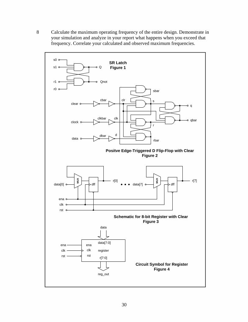
1. Using primitive gates, write a Verilog module for the SR Latch shown in Figure
1. Use a header similar to the one shown below, but use a suitable timescale for the delays indicated in point 3.
Save your module in a Verilog file with the same name as the module. 2. Using the SR_Latch2 module and primitive gates, write a Verilog module for the
positive edge triggered flip-flop shown in Figure 2. Use the following module header:
module dff(q, qbar, clock, data, clear);
output q, qbar; input clock, data, clear; o o o
endmodule
Save your module in a suitably-named .v file. 3. For all your models, use the following delay data: Single-input gates: intrinsic delay of 2 ns. Two-input gates: intrinsic delay of 3 ns. Three-input gates: intrinsic delay of 4 ns. Capacitive loading of 0.3 ns for a fanout of one. Capacitive loading of 0.5 ns for a fanout of two. Capacitive loading of 0.8 ns for a fanout of three. 1.5 ns loading delay for a primary output. You may assume infinite drive (zero delay) for all primary inputs.
Note that the instances of the SR latch have different delays, depending on where they are located in the overall design. You must find a solution for setting proper delays while still using three instances of the original design. There are several
29
ways to make this work. Creating different designs, one for each delay characteristic, is not an acceptable solution.
4 Write a Verilog model of the 8-bit register with the organization shown in
Figure 3. The register has the logic symbol shown in Figure 4. From its symbol, the functions of the register’s reset (rst) and enable (ena) can be inferred. Use the following module header:
module register(r, clock, data, ena, rst); output [7:0] r; input [7:0] data; input clock, ena, rst; o o o
endmodule
5 Write a testbench module, reg_test.v to verify the functionality of your design. Include stimuli to test the following: a. The register resets when rst is zero. b. The contents of the data bus are clocked into the register when ena is
asserted. c. The contents of the register are preserved and the contents of the data bus
are ignored when the register is clocked with ena deasserted.
6 Incorporate a clock generator with a suitable period for your design in your test fixture. 7 To reduce typographical errors, put your invocation of the compiler into a force
file. This is a text file that contains all the commands and arguments you would otherwise have to type in on the command line with each invocation of the compiler.
For example, if you have design files FileA.sv and FileB.sv and test fixture file
tb_TOP.sv, your force file would consist of vcs –debug –sverilog FileA.sv FileB.sv tb_TOP.sv Save the force file in a suitable file time with a .f extension. By default, Linux files are not executable. Make your force file executable by
typing from the command line chmod +x <filename>.f
30
8 Calculate the maximum operating frequency of the entire design. Demonstrate in your simulation and analyze in your report what happens when you exceed that frequency. Correlate your calculated and observed maximum frequencies.
Q
Qnot
s0
s1
r1
r0
SR LatchFigure 1
q
qbar
clear
clock
d
Positve Edge-Triggered D Flip-Flop with ClearFigure 2
rbar
r
sbar
scbar clr
clkbar clk
dbardata
MU
X
data[0] dffr[0]
ena
clk
rst
MU
X
data[7] dffr[7]
Schematic for 8-bit Register with ClearFigure 3
register
Circuit Symbol for RegisterFigure 4
ena
clk
rst
ena
clk
rst
data
data[7:0]
r[7:0]
reg_out
31
Experiment #4, Behavioral Modeling of a 5-bit Counter
1. Create a behavioral model of a 5-bit reloadable up counter.
a. Use the following timescale, inputs and outputs: Single bit inputs CLK, RST, LOAD, ENABLE Five bit input DATA Five bit output CNT 1 ns/1ns timescale Save your file as counter.sv. b. Model RST as an asynchronous, active low input.
c. Model LOAD as a synchronous, active high input. When asserted, the value on the data pins is loaded into the counter after the positive edge of the clock. d. Model ENABLE as a synchronous, active high input. When asserted, the count is incremented or loaded with new data (if LOAD is high). If ENABLE is not asserted, the counter will hold its value. The counter does not load new data if it is not enabled.
e. When LOAD is low, ENABLE is high and RST is high, the counter advances on the positive edge of the clock.
Counter
load
enable
clock
reset
cnt[4:0]
data[4:0]
32
2. Create a module for the asynchronous assert, synchronous de-assert function as described in class. 3. Integrate the two design modules into a top-level design unit. The AASD circuit should be at the same level as the counter, not embedded in it. 4. Create a test bench that does the following: a. Instantiates your top level design.
b. Provides a clock generator with a 10 ns period. c. Demonstrates an asynchronous reset. d. Show the counter initiates incrementing after reset is released. After it reaches a count of 4, parallel load 12 decimal. e. Demonstrate that it will count from 12 until the counter rolls over (i.e. returns to zero) and then starts counting back up. f. Demonstrates that reset overrides both load and increment. g. Demonstrates the correct functioning of enable.
33
Experiment #5, Scalable Multiplexer
Sca
labl
eM
ultip
lexe
r
a[size-1:0]
out[size-1:0]
b[size-1:0]
sel
Exp5_aa.vsd
1. Create a Verilog model of a scalable multiplexer, scale_mux.v. Use the following module header:
a. The size of the ports is determined by a parameter, SIZE. If the multiplexer is not scaled when instantiated, it defaults to one bit wide.
b. Use synthesizable, behavioral Verilog to write the multiplexer module. Note that there are several ways to code up the design, but you must not do anything that explicitly or implicitly includes any comparison to x. c. Your design should function such that input a should be selected when sel = 0 and input b when sel = 1. When sel = x, your multiplexers should resolve any bits for which a and b are the same. Any bits in conflict should result in x outputs.
2. Create a Verilog testbench to verify that the scalable multiplexer works. In the test module, create four instances of the scalable multiplexer. Use the three least significant digits of your student ID that are greater than 1 but not identical and one for the widths of the multiplexer data paths. For example, if your student ID is 100462983, you will use 1, 3 and 8 and 9. If your student ID is 54660101, you would use 6, 5, 4 and 1. Use three different methods of parameter redefinition to change the widths of three of the instances. Leave the fourth instance with its default width of one bit. i.e. don’t attempt to set a width. Test each instance to show that all specifications are met. (Note: This is one testbench with four instances, not four testbenches with one instance each). Drive the
34
largest multiplexer with as many bits as it needs for its a and b inputs. Use as many of the least significant bits of the a and b buses as needed to drive the smaller instances. The test vectors for the largest multiplexer should be sufficient to also test the smaller multiplexers. NOTE: when testing sel = 1’bx, you must apply a = b and a b cases and at least one case where a and b share some common bits and some opposite bits. Does your model function the same as the gate-level model simulated in Lab 1? Should it?
35
Experiment #6, Carry Select Adder The attached circuit diagram represents a 6-bit Carry Select Adder. It is one of the fastest adder circuits and has much better performance than a regular Ripple Carry Adder. Each adder stage, with the exception of the first one, consists of two sets of full adders and a multiplexer circuit. One set of full adders generates the sum and carry bits for the carry-in = 0 case and the other generates the sum and carry bits for the carry-in = 1 case. The carry out of each stage selects the correct sum and carry bits for the following stage. 1. Construct a full adder module using behavioral modeling.
Use a specify block to specify the following delays:
a or b to sum, 6 ns a or b or c_in to c_out, 2 ns c_in to sum, 3 ns
2. Construct a 2:1 mux module using behavioral modeling.
Use a specify block to specify the following delays: x or y to out, 2 ns sel to out, 3 ns
3. Using two pairs of full adder modules and two mux modules, develop a medium-level
module that generates a 2-bit sum. Use supply0 and supply1 nets to implement the logic 0 and logic 1 carries-in.
4. Using your medium level module, develop the full 6-bit Carry Select Adder module.
Use the following header:
module Carry_Sel_Adder(c6, sum, A, B, c0); o o o
endmodule 5. Write a non-exhaustive testbench to test the functionality of your adder. Select a
small number of robust test vectors. n.b. “small” no more than ten. Your test strategy should discuss why you chose the particular vectors you did. Why do you think the chosen set is robust? What, if anything, is not tested by the chosen set?
6. Write an exhaustive testbench to test your adder (including carry-in!) Compare your
adder’s output to the output of a 6-bit behavioral adder (including carry-out!). If they agree, continue testing until all inputs have been presented. If no errors were found, indicate the test was successful. If the adders do not agree, indicate the test has failed and show the operands and the expected and actual outputs. Stop testing when the first error is found or when all test vectors have been successfully applied.
36
7. To prove your exhaustive testbench will find an error, use a force assignment to override the behavioral adder’s sum sometime after ¾ of the test vectors have been applied. Use the `ifdef and `endif compiler directives to include or exclude the code that forces an error.
In your report, include log printouts from both the error-free and forced error cases. Use $monitoroff and $monitoron commands to show only the first dozen or so test vectors (and results) and the last dozen or so for the error free case. For the forced error case, use them to show the first dozen or so test vectors and about a dozen test vectors before and including the forced error. For the error-free case, include SimVision printouts showing the start and end of the test in sufficient detail to verify the applied signals and how they change. You may, if you wish, submit one or more “overview” printouts as well. For the forced error case, include SimVision printouts of the end of the test in sufficient detail to see when and how the forced error is applied and how the modules react. To make your output easy to analyze, use decimal numbers and show input values, output values and expected output values.
MUX MUX
FAFA
FA
FA
a5 b5
MUX
FA
FA
a4 b4
1
0
MUX MUX
FA
FA
a3 b3
MUX
FA
FA
a2 b2
1
0
a1 b1 a0 b0
c0
c6 s5 s4 s3 s2 s1 s0
FA =Full Adder
sum
carryin
carryout
a b
MUX sel
out
x y
Carry Select Adder
c2
c4
sel out0 x1 y
40
Experiment #7, Register File Model
A register file operates similarly to random access memory but is made from flopflops rather than DRAM or SRAM cells. A register file would consume far more power and take far more area than a true memory of the same capacity. However, register files have the advantages of operating fast, faster even than SRAM, and they can easily be coded in any arbitrary size (width and depth) in Verilog. In this lab, you will create a register file that will be used as a random access memory. Use parameters for both width and depth in your model. Where specific sizes are given in the description below, make those the default values for your parameters. 1. Create a Verilog model of a register file with the following specifications:
a. The memory has an eight bit bi-directional data bus. b. The memory has a five bit address bus. c. The output enable (oe) signal is active high. d. Chip select (cs) is active low. e. The value on the data bus is written to the address on the address bus after the
rising edge of the write strobe (ws). f. The contents of the currently specified address are placed on the data bus when
oe is high. g. Block read: as long as oe remains high, the contents of the newly specified
address are placed on the data bus. h. The data bus returns to the high impedance state after oe goes low. i. The chip select signal, cs, must be low to read or write. If it’s high, oe and ws
are ignored and the data bus remains in the high impedance state.
41
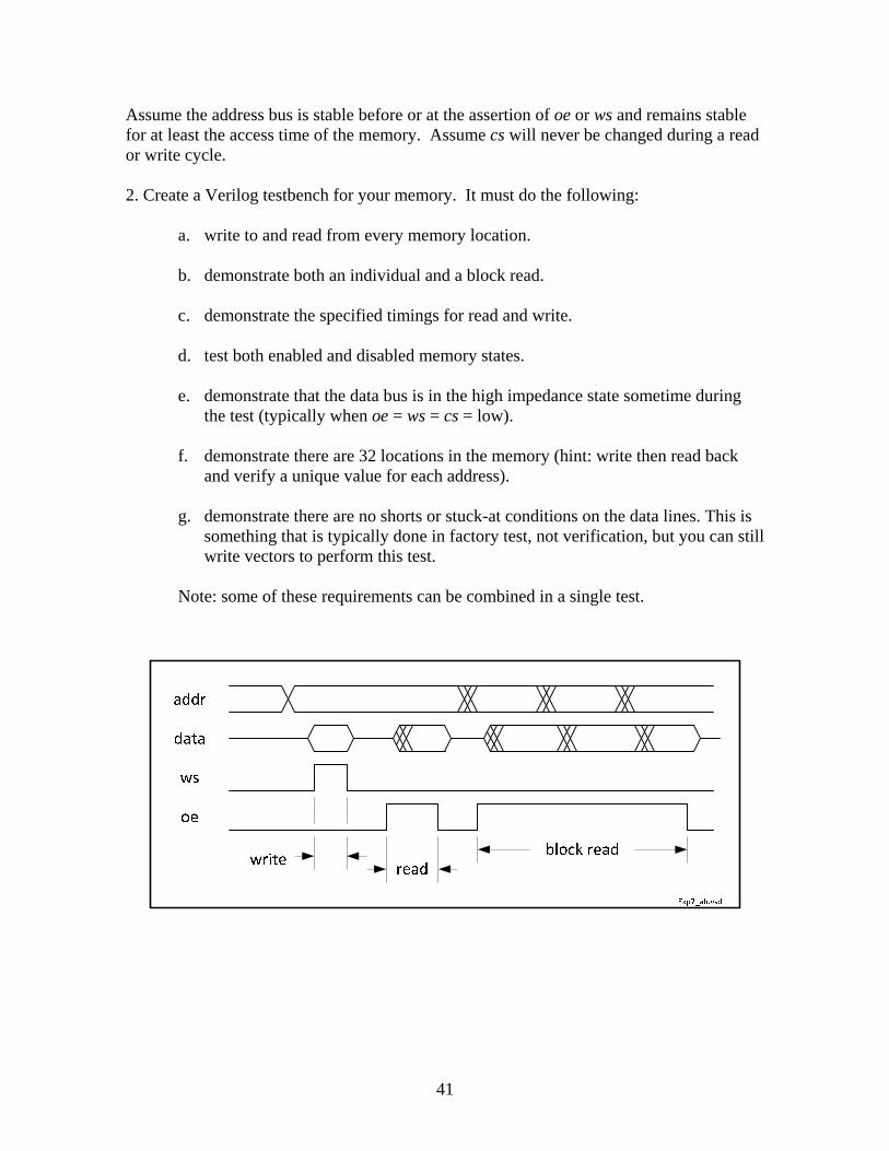
Assume the address bus is stable before or at the assertion of oe or ws and remains stable for at least the access time of the memory. Assume cs will never be changed during a read or write cycle. 2. Create a Verilog testbench for your memory. It must do the following:
a. write to and read from every memory location. b. demonstrate both an individual and a block read. c. demonstrate the specified timings for read and write. d. test both enabled and disabled memory states. e. demonstrate that the data bus is in the high impedance state sometime during
the test (typically when oe = ws = cs = low). f. demonstrate there are 32 locations in the memory (hint: write then read back
and verify a unique value for each address). g. demonstrate there are no shorts or stuck-at conditions on the data lines. This is
something that is typically done in factory test, not verification, but you can still write vectors to perform this test.
Note: some of these requirements can be combined in a single test.
42
3. Create a second Verilog testbench that does the following:
a. initializes the memory to the following hex values using the $readmemh system task: addresses 5’h04 to 5’h0F: 58 ED B7 34 C9 8F A0 9B 65 11 03 4C addresses 5’h10 to 5’h17: DA 7E F2 26 86 95 FD B1 addresses 5’h1C to 5’h1E: 12 AF 33
b. demonstrates the memory has been successfully initialized. c. demonstrates that unspecified locations remain undefined. d. reads locations 5’h10 to 5’h17, scrambles each byte, and writes the new byte back into memory. Each original byte is ordered [7654 3210], the new bytes are ordered [0716 2534]. e.g. 8’hDA becomes 8’h73. e. demonstrates the memory bytes have been successfully scrambled.
Use a task to print the contents of all memory locations as a 4x8 or 2x16 matrix. To show parts a through e have been accomplished, invoke the task before and after initialization and again after scrambling the data bytes. Waveform printouts must be detailed enough to verify bus timing and content of address and data buses (zoom in until numbers are readable). Include a printout of your $readmemh data file.
In your report, clearly state how many edge constructs you use in your model and why that is the best answer for this design.
43
Experiment #8, Arithmetic-Logic Unit Modeling In this experiment, you will model an arithmetic-logic unit, or ALU.
1. Create a Verilog module of the ALU. Use the following header:
output [WIDTH - 1:0] ALU_OUT; output CF, OF, SF, ZF; input [3:0] OPCODE; input [WIDTH - 1:0] A, B; input CLK, EN; o o o
endmodule Save your file as alu.sv. Use localparams for all the opcodes, but avoid use of any Verilog keywords for any opcodes. Note that the built-in Boolean primitives do match some of the opcodes and these names should thus not be used for any localparam names. Remember that while the simulator is case sensitive, downstream tools may not be. The ALU will support the instructions listed in Table 1. All opcodes not listed will not cause any change in ALU outputs. If the ALU is not enabled (EN is logic 0), all outputs will maintain their previous state.
44
Lab 8 Table 1: Opcodes and Actions Opcode Action 4'b0010 A + B 4’b0011 A - B 4’b0100 A and B 4’b0101 A or B 4’b0110 A xor B 4’b0111 not A
The ALU has Overflow, Negative, Zero and Carry flags. These flags are to hold their values between operations that update them. Overflow and Carry are only updated on arithmetic (addition or subtraction) operations. Both arithmetic and Boolean operations will update the other two flags. Overflow is an indication that a signed operation was too big for the ALU. It is detected by having the sign bit take an incorrect value. Adding two positive numbers and getting a negative result would cause the overflow flag to be set, as would adding two negative numbers and getting a positive sum. Note that since this is a clocked module, the output and the operands that are used to form the output are never available at the same time. Getting the overflow flag to operate correctly for subtraction is convoluted if Verilog subtraction is used. However, if the two’s complement of B is first taken and that is then added to A, the flag operation is unchanged from that used for addition. Carry is set when an addition or subtraction results in a carry out of the MSB position. While the definition for addition carry is clear and universally accepted, that is not the case for subtraction borrow. In this lab, use the Intel definition, which is that the bit is set for subtractions where A < B. The carry flag only has meaning when the operands are considered to be unsigned. Interpretation of the bit values (signed or unsigned) is up to the user of the computer. This applies to both the overflow and carry flags as well as to the data output. The Zero flag is set when the result is all zeros for any ALU operation. The Negative flag is set when the MSB of the ALU output is logic one. Again, negative is subject to interpretation by the user. As the hardware designer, you do not know or care how the operands will be interpreted by a programmer. Write a test plan to non-exhaustively but thoroughly verify your design. Implement your test plan in Verilog/SystemVerilog. Lab report question: should you use signed variables for the data path, that is, for A, B and ALU_OUT? Some experimentation will be required to adequately answer this question.
45
Experiment #9, Modeling a Sequence Controller
SequenceController
Addr[5:0]
Opcode[3:0]
Phase[2:0]
ALU Flags
A_EN
B_EN
PDR_EN
PORT_EN
PC_EN
PC_LOAD
MEM_CS
MEM_OE
MAR_EN
ADDR_SEL
I Flag
IR_EN
ALU_EN
PORT_RD
Lab 9 Figure 1: Sequencer Inputs and Outputs A. Creating a Sequence Controller Module Create a SystemVerilog behavioral module of the sequence controller shown above. Call it control.sv. Table 4 in this section has a decoding key explaining the meaning of each output. Each instruction will take eight clock cycles to complete. A three-bit phase generator module is included to facilitate decoding of the cycles and associating each cycle with certain sequencer actions. This simplistic implementation is deliberately inefficient. There is no technical reason that would prevent some of the actions taken in different cycles from happening concurrently, shortening the time each instruction takes and increasing throughput. When reset is asserted (logic 0), the phase is set to zero, which corresponds to enumerated type FETCH.
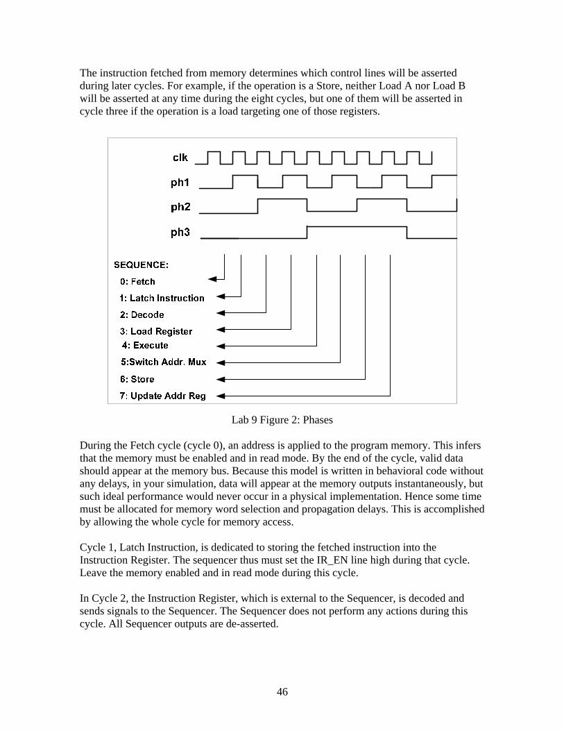
46
The instruction fetched from memory determines which control lines will be asserted during later cycles. For example, if the operation is a Store, neither Load A nor Load B will be asserted at any time during the eight cycles, but one of them will be asserted in cycle three if the operation is a load targeting one of those registers.
Lab 9 Figure 2: Phases
During the Fetch cycle (cycle 0), an address is applied to the program memory. This infers that the memory must be enabled and in read mode. By the end of the cycle, valid data should appear at the memory bus. Because this model is written in behavioral code without any delays, in your simulation, data will appear at the memory outputs instantaneously, but such ideal performance would never occur in a physical implementation. Hence some time must be allocated for memory word selection and propagation delays. This is accomplished by allowing the whole cycle for memory access. Cycle 1, Latch Instruction, is dedicated to storing the fetched instruction into the Instruction Register. The sequencer thus must set the IR_EN line high during that cycle. Leave the memory enabled and in read mode during this cycle. In Cycle 2, the Instruction Register, which is external to the Sequencer, is decoded and sends signals to the Sequencer. The Sequencer does not perform any actions during this cycle. All Sequencer outputs are de-asserted.
47
During the Load Register cycle (Cycle 3), immediate data are latched into one of the registers according to signals sent from the Instruction Register. Immediate data means that the data are contained in the instruction, as opposed to being stored in a different memory location. When data must be fetched from a different memory location, the registers will be loaded in Cycle 6 rather than Cycle 3. Immediate data are signaled by setting the I Flag. There are five registers that may be enabled during the Load Register cycle: A and B of the ALU, the Port Direction Register, the Port Data Register and the Memory Address Register. The sequencer needs one output for each so that it can enable the appropriate one during this cycle. The sequencer also needs to control the memory address bus selector, the memory output enable and the memory chip select. If the opcode is an ALU operation, the ALU will be enabled in Cycle 4 (EXECUTE cycle). Cycle 5 is used for setting up memory access in Load and Store operations. In both cases, the memory address bus must be switched to use the address from the Memory Address Register rather than the Program Counter. In Cycle 6, ALU output data or port IO data are written to memory if the operation is a store. In the case of Load, data from the memory are latched into the selected target register in this cycle. In Cycle 7, the Program Counter is updated. The PC is external to the Sequencer but needs to be enabled by the Sequencer. It can either be incremented or loaded with a new value. It has two control signals, both set by the Sequencer: Enable and Load. Enable will always be activated in Cycle 7. Load will only be activated if a Branch or Jump is to be performed. This is determined by decoding both the opcode and the four ALU flags. If the opcode is Jump, Load will be activated. If it is BZ, it will be activated only if the Z flag is set. If it is BN, it will be activated only if the N flag is set, etc. Each instruction will have the following format:
Lab 9 Table 1: Instruction Format Bits Field Meaning 31 : 28 Opcode 27 Immediate flag: if set, bits 7:0 are immediate data. 26 : 21 Load/Store Address 20 : 8 Reserved 7 : 0 Immediate data Table 1 is for reference only in this lab. For this lab, the various fields are already broken out as inputs to the sequencer as needed. The data field is not used in this lab. Note that although there are Load and Store opcodes as well as Load and Store phase states, they are not the same thing. There is no direct correlation between them. It would be
48
illegal to use one as a localparam and one as a typedef in the same scope anywhere in the design.
Clock
Ph1
Ph2
Ph3
Reset
X
X
X
Lab 9 Figure 3: Phase Generator Signals. Use Enumerated Types for the eight states.
Memory mapping The RISC processor for which this is the controller will be memory mapped as shown in Table 2. This means that in addition to the 32-deep combined program and data memory, some machine registers and the I/O port will also be enabled for reading and writing when addressed. Enabling memory mapped devices requires reading the address bus along with the opcode. When addressing a memory-mapped register, the main memory should be disabled.
Lab 9 Table 2: Memory Map Decimal Address Device 0-31 Memory 32 ALU A Register 33 ALU B Register 34 Port Direction Register 35 I/O Port 36 Memory Address Register
Any address not covered by the above table is not implemented. Reading from an unimplemented address will produce unpredictable results. Writing to an unimplemented address will have no effect. Note that I/O Port read and write share the same address. Setting the enables is distinguished by the opcode: when LOAD, data are written to the Port Data Register. When STORE, the I/O Port drives data onto the bidirectional memory bus. To avoid contention, the memory output must be disabled when the port is driving, though the memory chip select must remain active so that new data may be written to the memory. The instruction set for the CPU is shown in Table 3 below. Any opcode not covered shall be illegal. You do not need to do anything in hardware to detect illegal input conditions.
49
Lab 9 Table 3: Instruction Set MNEMONIC INSTRUCTION OPCODE
LOAD Load a register 4'b0000 STORE Store ALU Output 4’b0001 ADD Add A and B 4’b0010 SUB Subtract B from A 4’b0011 AND Bitwise AND of A and B 4’b0100 OR Bitwise OR of A and B 4’b0101
XOR Bitwise XOR of A and B 4’b0110 NOT Bitwise inversion of A 4’b0111
B Unconditional Branch 4’b1000 BZ Branch if Z flag is set 4’b1001 BN Branch if N flag is set 4’b1010 BV Branch if OVF flag is set 4’b1011 BC Branch if C flag is set 4’b1100
Lab 9 Table 4: Sequencer Output Key
Pin Name Function IR_EN Enable writing to Instruction Register A_EN Enable writing to ALU A register B_EN Enable writing to ALU B register PDR_EN Enable writing to Port Direction Register PORT_EN Enable writing to Port Data Register PORT_RD Enable reading Port Input Data PC_EN Enable updating Program Counter Register PC_LOAD Enable parallel load of PC. Only works if PC_EN is also active MAR_EN Enable writing to memory address register for data load/store ADDR_SEL Switch memory address bus from PC to memory address register MEM_OE Memory output enable. High for memory read, low for write MEM_CS* Memory Chip Select: necessary for any memory access, read or write *MEM_CS (Memory Chip Select) is active low. All other enable signals are active high. No matter how the module is coded, the inferred circuit must be totally synchronous, other than the asynchronous assertion of reset. This means that each and every flipflop in the design receives the same phase of the master clock, which is clk in the diagrams. This requirement may appear be at variance with diagrams and other text in this document. These synchronous design rules apply equally to Experiment 10. There is no one correct way to code the sequencer. It can be done as a classic state machine. An equally correct design can be made as a series of conditional statements. Your goal is to produce an elegant, easy to understand and easy to maintain design. While minimal coding length is not in and of itself a goal, excessively long and convoluted code is definitely undesirable.
50
B. Creating the Clock Generator The clock is a primary input from the outside world. Slower periodic signals are derived from it in a Phase Generator block, which must be reset using an asynchronous assert, synchronous de-assert reset signal. Create a SystemVerilog behavioral module of the phase generator shown below (phaser.sv). Use the following module header:
module phaser(CLK, RST, EN, PHASE); o o o
endmodule PHASE is a three-bit output using enumerated types {FETCH, LATCH, DECODE, LOAD, EXECUTE, SWITCH, STORE, INCREMENT}. The three bits of the output must toggle as shown in the various illustrations, though they will be encoded together to form the eight enumerated types. Do not make eight outputs. Only three are needed. Only use SV methods for changing values of the phase. The enumerated type must be carried through to the top level and the sequencer.
phasegenerator
enablePhase [2:0]
Exp9_ea.vsd
clk
reset
Lab 9 Figure 4: Phase Generator
The phase generator produces timing signals as shown in the timing diagrams. It must be synchronous, using only the rising edge of the clock and the falling edge or reset to trigger output changes. There are several ways in which it can be coded but however it is done, it must not use any logic signal as a clock. C. Top level Combine the design modules into one top level design. Instantiate only the top level design in your test fixture. D. Testing with a Stimulus File Using a similar approach to the one used in Experiment #6, create an automated testbench to test all modules together. This test fixture must check all outputs and report that the
51
simulation either completed correctly or failed. Use force and release to inject errors and demonstrate that your test fixture is capable of detecting faulty operation. Use name declaration (dot naming) to connect signals between the testbench and the modules under test. List signals in reverse order from their original order in the module port list. Previously we have used positional declarations. Both your controller module and your testbench should be well documented. In particular since the testbench is automated, be sure you document your test strategy.
52
Experiment #10, Final Project: The RISC-Y CPU During the semester, you have modeled and simulated the following modules:
These modules can be put together to form the following RISC-Y CPU system. However, instead of instantiating the register from Lab 3, you will model several registers of appropriate sizes behaviorally. The RISC-Y processor is typical of modern Reduced Instruction Set Computer architectures such as the ARM family of processors used in virtually all smart phones in that it has a small, regular instruction set and a load-store architecture. Though it is far simpler and more stripped down than any current-production machine, it is a complete microprocessor and could be programmed to accomplish any general purpose computing task. Each RISC-Y instruction will use the following format:
Lab 10 Figure 1: Instruction Format
Bits [7:0] are immediate data. When the opcode is Load and the I bit (Bit 27) is set, these data are loaded into the target register indicated by the Address field (Bits [26:21]). If the I bit is not set, then the Data field contains the address of the data to be loaded into the target register. Since this implementation of the RISC-Y CPU only has 32 memory words, only the least significant bits of the Data field are used for the address pointer. These bits are loaded into the Memory Address Register for Load and Store operations other than Load Immediate. Note that the Address field needs six bits because the CPU has memory-mapped registers, but five bits are all that are needed for memory addressing. The RISC-Y CPU has only two addressing modes: Immediate and Direct. Immediate data are held in the Data field of the instruction. Direct data has the address of the data in the Data field. They are distinguished by the I bit. When the I bit is set, the addressing mode is Immediate. Otherwise, it is Direct.
53
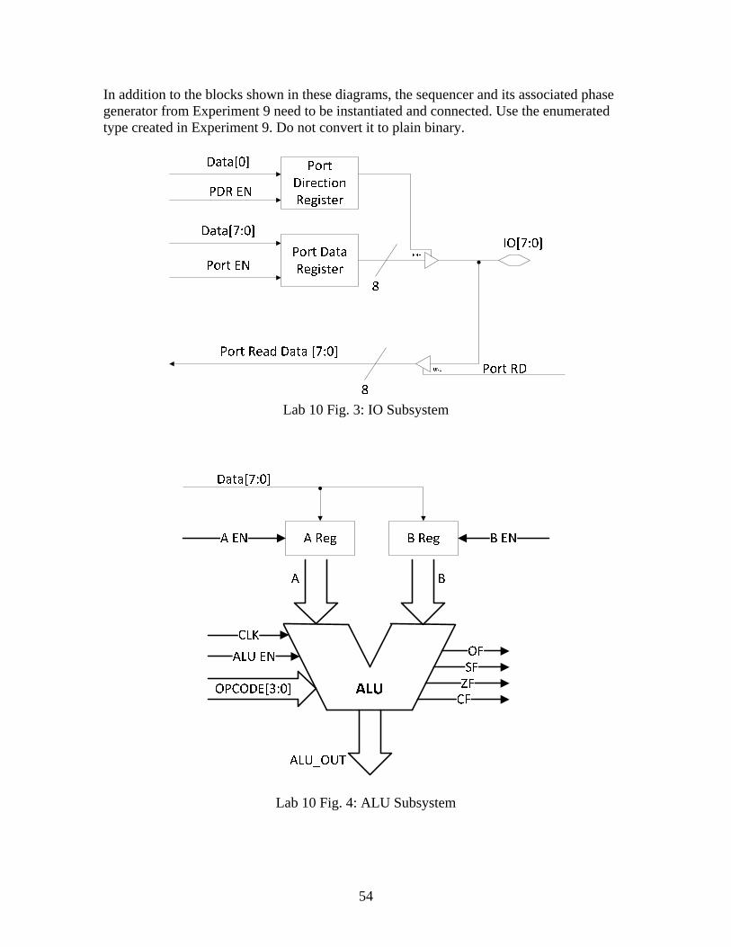
There are only two possible objects that may be stored: the ALU output and the port. When the opcode is STORE, the Address field is checked to see if it contains 35, which is the address of the port. If there is a match, port data are stored in the address indicated by the least significant bits of the Data field. For any other address, the ALU contents are stored. ALU opcodes (ADD, SUB, AND, OR, XOR and NOT) do not need to reference any fields other than the opcode. They always use the A and/or B registers for operands and the result always goes to the ALU results register. The remaining opcodes are all branches. For these operations, the branch address will be contained in the lowest five address bits. These bits are loaded into the Program Counter. The major component groups of the RISC-Y CPU are shown in Figures 2 through 4 below.
Lab 10 Fig. 2: RISC-Y Memory Subsystem
54
In addition to the blocks shown in these diagrams, the sequencer and its associated phase generator from Experiment 9 need to be instantiated and connected. Use the enumerated type created in Experiment 9. Do not convert it to plain binary.
Lab 10 Fig. 3: IO Subsystem
Lab 10 Fig. 4: ALU Subsystem
55
A. Creating a Verilog module for the RISC-Y CPU: 1. Create a Verilog module for the RISC-Y CPU (cpu.sv). Use the following module
endmodule 2. The RISC-Y CPU unit has the following specifications:
A Sequence Controller steps the CPU through a fetch instruction/fetch operand cycle. This sequence requires eight master clock cycles.
The memory will be 32 bits wide and 32 words deep, or 32 x 32.
The design is to be totally synchronous. The only clock is the master clock. No
derived signals may ever be used as a clock.
While it would be logically correct to use the primitive operator register design from lab 3, that function should be re-designed using behavioral code. The behavioral code should not have any delays specified.
The system shall use an asynchronous assert, synchronous de-assert reset. A
module implementing this function must be incorporated into the design. A Program Counter points to the next location in memory from which the CPU will
fetch instructions or data. The PC is the counter from Lab 4. It may be loaded with branch addresses or incremented to go on to the next address in sequence.
The ALU only receives operands from the A and B registers, which are eight bits
apiece.
There is one eight-bit input-output port. When it is an output, data can be written to it by executing a LOAD operation with the ports address (35) in the address field. It is read by performing a STORE operation with the store address in the data field and the port address of 35 in the address field.
56
When an eight bit quantity is loaded or stored, the active bits are always the eight
least significant of the referenced memory location.
The port direction is set by writing to the Port Direction Register, address 34. This is a one-bit register. To simplify the design, all bits operate together as either input or output.
Data for the one-bit Data Direction Register will take its data from the least significant bit of the referenced memory location. It can only be changed via a LOAD operation. There is no provision for reading this register.
The tristate data bus must never be allowed to float. Exactly one driver must always
be active. This means that some modification to the logic controlling memory read and write will be necessary to prevent a floating bus.
The CPU can process the following instructions:
Lab 10 Table 1: RISC-Y Instruction Set MNEMONIC INSTRUCTION OPCODE
LOAD Load a register 4'b0000 STORE Store data in memory* 4’b0001 ADD Add A and B 4’b0010 SUB Subtract B from A 4’b0011 AND Bitwise AND of A and B 4’b0100 OR Bitwise OR of A and B 4’b0101
XOR Bitwise XOR of A and B 4’b0110 NOT Bitwise inversion of A 4’b0111
B Unconditional Branch 4’b1000 BZ Branch if Z flag is set 4’b1001 BN Branch if N flag is set 4’b1010 BV Branch if OVF flag is set 4’b1011 BC Branch if C flag is set 4’b1100
*Only the ALU output or data read from the port may be directly stored. Store always refers to the ALU output unless the address of the port appears in the address field of the STORE instruction.
57
B. Testing with a Stimulus File: Create a testbench to verify the RISC-Y CPU module. To accomplish this, write a CPU program is and load it into the memory using $readmemh. After the system is reset, the processor should start executing your instructions. If all the components of the system are working properly, the CPU will:
Fetch an instruction from the RAM memory. Decode the instruction. Fetch a data operand from the RAM memory if required by the instruction. Perform any ALU operations required by the instruction. Store the result when so instructed. Repeat the cycle by fetching the next instruction.
All steps should be well documented and the results well presented! All instructions and conditions should be tested. Multiple test program files are likely to prove advantageous rather than trying to demonstrate correct functioning of all instructions in one file. Remember to zoom in so that submitted waveforms are readable. You may, if you wish, also submit one or more “zoomed out” overview plots.
58
Appendix A UNIX Command Reference Guide
59
UNIX Command Reference Guide
Note: Commands for the UNIX operating system are case sensitive, most of which need to be typed in lower case. Examples are underlined. HELP COMMANDS help An interactive facility for on-line
documentation. Type help general for more information.
apropos Finds commands that deal with a certain topic. apropos pascal will display commands pertaining to pascal.
man Displays information about a specific command. man mail will display information about the mail program. man -k graphics will display a list of man pages that pertain to graphics. Note: man -k is the same as apropos.
whatis Displays a short description about the function of a command. whatis mail will display a short description of mail.
GENERAL CONCEPTS C-key While holding down the control key
(also marked “Ctrl”), press the key after the dash. C-c means hold the control key and type “c”.
options Generally, UNIX command options are specified with a character or character string that begins with a “-” (dash). In the example man -k mail, “-k” is an option for the man command. Many times, the order or placement of options is significant.
CONTROL CHARACTERS RET Carriage Return. It sends a completed
command to the system. C-c Aborts (interrupts) the current
command or program. C-z Stops or suspends the current process. C-s Halts the scrolling of output to the
terminal. C-q Continues scrolling. C-o Stops (flushes) output from being seen
on the terminal. C-r Redisplays the command line. C-u Erases the command line. C-w Erases the last word on the command
line. DEL (Delete key) Deletes a single character from
the end of the command line. BREAK (Break key) Three BREAKs can disconnect
your terminal from the system in an emergency. SESSION CONTROL & PRIMARY COMMANDS passwd Invokes program to change login password. You
are prompted for old and new passwords. logout Terminates the login session. exit Exits the current shell. ps (with no options) shows your process. setenv Changes variables associated with your
environment. setenv printer l-phe108 sets your default printer to be the LPS-40 printer (ASCII mode) in PHE 108.
set Changes or sets variables known as shell variables. set prompt=MyPrompt: will change the prompt for your current shell to that particular string.
clear Clears the terminal screen. FILE MANIPULATION COMMANDS ls Displays (lists) contents of the current directory. pwd Displays the name of your currently active
directory, i.e. where you are in the file system. cd Changes to another directory. cd /etc will move
you to the directory named “etc”. cat Concatenates (sequentially displays) files.
cat proj1.c will display the file at your terminal. more Displays a file at your terminal and pauses at the
bottom of each page. more apple.p will display the file apple.p.
cp Copies a file. cp apple.p lemon.p creates a new file, lemon.p, which is identical to apple.p.
mv Renames a file. mv apple.p lemon.p will rename the file apple.p to the new name lemon.p.
chmod Changes the read, write and/or execute permissions (or modes) of a file.
mkdir Creates (makes) directories. rmdir Deletes (removes) directories. rm Deletes (removes) a file. Example: rm apple.p diff Displays the differences between two files.
Example: diff apple.p lemon.p sort Sorts the lines of a file alphabetically. sort a.list
will sort the lines in a.list into alphabetical order. col A post-processing filter that removes special
formatting characters. Useful for displaying man pages during a Telnet session or on a simple TTY. Example: man keyword | col -b.
find Finds all files along a specified path that meet certain conditions. find $HOME -ctime n finds all files in your home directory (and any subdirectories) that were modified in the last n days. (+ctime n finds files modified n or more days ago). find $HOME -name ‘filename’ finds all files in your home directory and any subdirectories matching the filename pattern. Wildcards can be used.
fgrep Searches for files containing lines matching a text pattern. pattern must be enclosed in single quotes – it is a text “literal”. fgrep -c ‘keyword’ filename prints a count of the number of lines containing keyword in the file filename. fgrep -f matchfile filename1 > filename2 copies all lines in filename1 that match any line in matchfile into file filename2. See also grep and egrep.
wc Counts the number of words and characters in a file. wc apple.c will display the number of words, characters and lines in the file apple.c.
60
wc -l apple.c will display only the number of lines in the file apple.c.
PRINTING COMMANDS lp Prints a file on the default printer. lp MyFile.ps
will print the MyFile.ps on the default printer. Use the -d device option to direct output to a specific device.
lpstat Displays the lp print queue status. cancel Cancels print requests made with lp. lp ID will
cancel a specific request. (Use lpstat to get ID). lpr Alternate print command on some systems,
similar to lp. Prints a file. lpr test.p will send file test.p to the printer. Use the -P option to specify a particular printer.
lpq Alternate print queue display command on some systems, similar to lpstat. Displays the print queue for a particular printer and gives your print request number.
lprm Alternate print request cancellation command. lprm -Px-sa1125 60 will cancel print request number 60 on printer x-sa1125.
COMPILATION/DEBUGGING COMMANDS cc Invokes the C compiler. f77 Invokes the FORTRAN-77 compiler pc Invokes the Pascal compiler dhx Invokes the symbolic debugger. You must first
compile your program with the debug option enabled.
INFORMATION COMMANDS date Displays the current date and time. finger Displays all users currently on the system. chfn Changes the information shown when someone
issues the finger command. cal Displays a calendar of the current month. Use
cal mo yr for a specific month or cal yr for a full year. (yr may be 1–9999 so all digits must be given).
COMMUNICATION COMMANDS mesg Allows you to receive or block messages to your
terminal. Options are y and n. write Puts you in direct communication with another
user. write user will allow you to communicate with user. Everything you type will appear on user’s terminal. To stop communication, press C-d on a new line.
ADVANCED FILE MANIPULATION
and REDIRECTION < Redirectes the input of a command to read from a
specified file. mail user < text.msg will send the letter contained in text.msg to the user named user.
> Redirects the output of a command to a specified file. If the file does not exist, it is created. If it already exists, the former contents are destroyed. ls > dir.log will put the names of the files in your directory in the file dir.log.
>> Like the > (redirect output) command except data is appended to an existing file rather than destroying the original contents.
| (Pipe). Connects the output of one command to the input of another. ls | mail user will send a listing of the names of your files to user.
tee Like the pipe (above) but sends the output to the terminal as well as to a file. ls tee dir.log will display the names of the files in your directory on your terminal and will put them in the file dir.log.
script Creates a log file which is a record of your terminal session. script myfile.log will create a file named myfile.log and will copy all text that is displayed on the monitor into myfile.log. If no filename is specified, the default file is typescript.
MAIL mail Enables sending and receiving of mail.
mail user will send an e-mail to user. Type the text of the letter following this command. Type C-d on a new line to end the letter and send it to user. If you have received mail, typing mail will allow you to read them (see also cmm).
? Shows a list of mail commands. h Displays a screen full of headers of the current
messages. t Displays a message on your terminal. t 2 will
display message number 2 on your terminal. n Displays the next message on your terminal. e Allows you to edit one of your messages. e 2
invokes the editor for message number 2. d Deletes a message. d 2 will delete message
number 2. u Undeletes a message. u 2 will undelete message
number 2. s Appends (saves) a message to a file. s 2 msg.txt
will put message 2 at the end of the file msg.txt. r Replies to a message. r 2 will send a reply to the
sender of message number 2. m Will send mail to another user. m user will
send mail to user. q Quits the mail program, expurges deleted
messages and moves (by default) current messages to a file named mbox in your home directory.
x Quits the mail program without changing the system mailbox.
61
Appendix B vi Editor Command Reference Guide
62
vi Editor Command Reference Guide
The variable n indicates a number as part of a command. Where this variable is enclosed in parenthesis, it represents an optional number argument. For example, (n)^D indicates that the ^D command may or may not be preceded by a number.
Unless otherwise stated, all escape mode cursor movements can be the address of any escape mode editing command that takes a following address.
EXITING vi :w Writes the editing buffer to disk. If you specify
a following filename, writes the buffer to a file with that name.
:q Exits vi without writing to disk. :wq Writes the file to disk and then quits. :x Writes the buffer to disk only if changes have
been made since the last write then quits. ZZ Same as :x. Q Puts you in ex command mode. Use the ex
command vi to get back into visual mode. CURSOR MOVEMENTS b Moves back one word (bounded by punctuation
or whitespace). B M oves back one word (bounded by whitespace). e Moves to the end of current or next word. E Moves to the end word until whitespace character. f Moves to next occurrence on the current line of
the character you type next. Fx Moves to previous occurrence on the current line
of the character you type next. (n)G Moves to last line of file or line number n. h Move back one space. j Moves down one line. k Moves up one line. l Moves forward one space. (n)L Moves to bottom of screen or n lines from bottom. M Moves to beginning of middle line of screen. tx Moves to the space before the next occurrence of
character x on the current line. Tx Same as t but scans backwards on current line. w Moves to beginning of next word (bounded by
punctuation or whitespace). W Moves to beginning of next word (bounded by
whitespace). S Moves to last character of current line. % Moves to ), ], or } matching next occurrence of (, [
or {, respectively. ^ Moves to first nonwhitespace character on current
line. ( Moves to beginning of current or previous
sentence. ) Moves to beginning of next sentence. & Repeats last substitution (executed with last line
command s) on current line. { Moves to beginning of current or previous
paragraph where a paragraph is marked with one of the nroff paragraph macros. Type :set all to see what these are.
} Moves to beginning of next paragraph (see preceding command).
[[ Moves to beginning of current or preceding section where a section is marked with one of the nroff paragraph macros. Type :set all to see what these are.
]] Moves to beginning of next section (see preceding command).
“ Moves to location where last major motion command was given.
‘ Repeats last search with f, F, t, or T, but reverses direction.
‘x Moves to exact location on line marked x (marked with the m command).
`x Move to the start of the line maked with x (marked with the m command).
+ Moves up one line. - Moves down one line. SCREEN CONTROL COMMAND ^F Pages forward one screenful. Cannot be used as a
cursor movement address. ^B Pages back one screenful. Cannot be used as a
cursor movement address. (n)^D Scrolls down half a screen or n lines. Cannot be
used as a cursor movement address. (n)^U Scrolls up half a screen or n lines. Cannot be used
as a cursor movement address. ^R or ^L Redraws the screen when it has been scrambled by
a system message, a message from another user, or some other interruption.
(n)zsize Redraws the screen with the current line or line n at the top of the screen. If size is specified, the screen is redrawn with that number of lines.
(n)zsize. Redraws the screen with the current line or line n at the middle of the screen. If size is specified, the screen is redrawn with that number of lines.
(n)zsize_ Redraws the screen with the current line or line n at the bottom of the screen. If size is specified, the screen is redrawn with that number of lines.
EDITING COMMANDS a Appends text after the cursor. A Appends text at end of current line. cc Changes one line to the next text typed. cx Changes from cursor to place delimited by cursor
movement x. C Changes current line from cursor to end. dd Deletes one line. dx Deletes from cursor to place delimited by cursor
movement x. D Deletes from cursor to end of current line. i Inserts text before the cursor. I Inserts text at beginning of current line. J Joins current line and next line. mx Marks current line (and current cursor position)
with letter x. o Opens new line below the current line. O Opens new line above the current line.
63
p Replaces last deleted, copied or changed text after the cursor.
“np Places text in delete buffer n after the cursor. “xp Places text in named delete buffer x after the cursor. P Replaces last deleted, copied or changed text before
the cursor. “nP Places text in delete buffer n before the cursor. “xP Places text in named delete buffer x before the
cursor. r Replaces the character the cursor is on with the next
character typed. R Replaces one character at a time with characters
typed next. s Substitute the next character typed for the character
the cursor is on. S Changes current line (identical to cc). u Undoes last editing command. U Undoes all editing changes to the current line. x Deletes character the cursor is on. X Deletes character before the cursor. yy Copies current line. Y Copies current line (identical to yy). “xyy Copies current line into delete buffer x. & Repeats last substitution (last line command) on
current line (pattern must be matched). ~ Changes the case of the letter the cursor is on
(upper to lower or lower to upper). Cannot be preceded by a number.
(n)> Shifts n lines right by the value of the ShiftWidth option.
(n)< Shifts n lines left by the value of the ShiftWidth option.
SEARCHING f Finds next occurrence on the current line of the
character typed next. F Finds previous occurrence on the current line of the
character typed next. tx Moves to the space before the next occurrence of
character x on the current line. Tx Same as t but scans backwards on the current line. , (comma). Repeats last search with f, F, t or T but
reverses direction. /expr Searches for next occurrence of expr (any regular
expression in the file.
?expr Searches for previous occurrence of expr (any
regular expression in the file. n Repeats last search with / or ?. N Repeats last search with / or ? but reverses direction
of search. MISCELLANEOUS ESCAPE MODE COMMANDS “x Names delete buffers. Puts next deleted, changed
or copied text in named buffer x. ^G Displays at the bottom of the screen the current line
number and information about the length of the file. mx Marks current line (and current cursor position)
with letter x. LAST LINE EDITING COMMANDS x,y(d) Deletes lines with addresses x through y. x,y (m)z Moves lines with addresses x through y to below
line with address z. x,y (co)z Copies lines with addresses x through y to below
line with address z. x,y s/pat1/pat2/(g)(c) Replaces search pattern pat1
with replacement pattern pat2 on lines with addresses x through y. If g is set, substitutes for every occurrence of pat1 on specified lines. If c is set, asks you to confirm each substitution.
g/pat1/s//pat2/(g)(c) Same as above but makes substitution on every line in the file containing pat1.
vi ENVIRONMENT OPTIONS all Displays a list of all the currently set option values. autoindent (ai) Used for writing structured programs
where indentation is important for determining levels of embedded commands. When set, vi indents each line you type an appropriate amount dependent on the indentation of the previous line.
autoprint (ap) Displays the current line after each copy, move, or substitution (s) command.
ignorecase When set, the case of letters in regular expressions (in search patterns) is ignored except in ranges within square brackets.
magic When nomagic is set, all magic characters (used in regular expressions) except ^ (beginning of line) and $ (end of line) lose their magic properties. By default, magic is set but even when nomagic is set, you can turn on the magic of individual characters by preceding them with \ (backslash).
mesg By default, nomesg is set. When set, mesg allows other users to write to your terminal with the write command which can temporarily scramble your screen.
number When set, the number of each line is displayed at the left of the screen.
report report=5 is set by default. This option determines the threshold at which the number of lines deleted, copied, moved or changed is reported.
showmatch When this optionis set, each time a ) or } is typed in insert mode, the cursor jumps quickly back to show the matching ( or {.
showmode Causes the message “INPUT MODE” to be displayed in the lower right corner of the screen when you are in insert mode.
wrapmargin By default, wrapmargin=0 is set. When a different numerical value is set, causes a RETURN to be inserted that number of characters from the right edge of the screen in insert mode.
64
wrapscan When set, vi treats a file as a continuous loop for searches with / and ?. When nowrapscan is set, a search with / stops scanning when it reaches the end of the file and a search with ? stops scanning when it reaches the beginning of the file.
MISCELLANEOUS LAST LINE COMMANDS = Displays the current line number. :ab str1 str2 Designates str1 as an abbreviation that
will expand to str2 (any word or phrase) when typed in insert mode.
:unab str Unabbreviates (removes the special significance of)
str, a string abbreviation specified with :ab command.
:map str1 str2 Maps str1, where str1 is any sequence of characters, that will expand to str2 when typed in escape mode.
:unmap str Unmaps str, a string mapped with the
map command. (address1, address2) w (file) Writes lines with addresses
address1 through address2 to a file called file. (address) r file Reads the file file into the current file
below the current line. If an address is specified, reads the file in below the specified line.