ELSEVIER Journal of Crystal Growth 172 (1997) 337-349
, . . . . . . . . C R Y S T A L G R O W T H
Eddy current sensing of vertical Bridgman growth of Cdo96Znoo4Te
Kumar P. Dharmasena, Haydn N.G. Wadley * hltelligent Processing ()[Materials b~boratot T, School (~[" Engineerin~ and Applied Science, University (~f Virginia, Charlottesz'ille, Virginia
22903, USA
Received 21 August 1995: accepted 17 April 1996
A b s t r a c t
An encircling two coil eddy current sensor has been integrated into the ceramic liner of a commercial six zone vertical Bridgman furnace and used to monitor the growth of 72 mm diameter Cd0.96Zno.o4Te crystals. The sensor was maintained at a fixed location with respect to the ampoule and monitored melt cooling/composition, detected the position of the liquid-solid interface, measured the interface's curvature and determined the electrical resistivity of the solid during post-solidification cooling. The study confirmed earlier predictions that a two coil, multifrequency sensor approach can independently recover the liquid-solid interface location and provide insight about its curvature using data collected in the 50 kHz to 5 MHz frequency range. It suggests that the directional solidification of Cdo.96Zno.o4Te most probably initiates from a Cd-depleted melt, occurs in a colder than anticipated region of the furnace and progresses with a convex interface shape.
1 . I n t r o d u c t i o n
High performance infrared focal plane arrays (IRFPAs) for infrared imaging systems can be pro- duced by depositing Hg I _ ,Cd,Te infrared detector films on infrared transparent substrates such as CdTe [1-4]. Recently, 3%-5% atomic Zn has been added to CdTe substrates to increase their high temperature yield stress and provide better lattice matching with the detector material [1,4-7]. The single crystal sub- strates needed for IRFPA applications are normally "mined" from large polycrystalline boules made by the unseeded di rec t ional sol idi f icat ion o f Cd~ ~Zn~Te melts using either a vertical [6,8-12] or
Corresponding author.
horizontal [13-16] variant of the Bridgman process. In spite of intensive efforts by many groups [17-19] to experimentally optimize furnace temperature pro- files, ampoule geometries/materials, charge material purity/stoichiometry and the growth (i.e. furnace translation) rate, the ultimate yield of Cdt_~Zn,Te suitable for large area (e.g. 4 cm × 6 cm) substrates remains disappointingly low ( < 10%).
The reasons for yield loss are many and complex, but amongst the most important are the polycrys- talline nature of the boules, macrosegregation of Zn [20], high dislocation densities ( > 105 cm -~) [21] and low ( < 0.65 of theoretical) infrared transmission due to inhomogeneities (principally Te inclusions or precipitates greater than 10 /xm in diameter) [22]. The poor yield directly affects the affordability of these substrates. It also results in the need for exten-
sive characterization and screening which further increases the cost of substrate manufacture. Since most of the yield loss is associated with the solidifi- cation process, intensive efforts are under way to improve this technology.
Several groups are attempting to model the solidi- fication process [10,12,23-28]. This requires incor- porating heat transport by conduction and convective flows within the melt, as well as addressing the moving (liquid-solid) boundary and the segregation of Zn. Other work seeks to model the differential thermal contractions on cooling and predict the dis- location density and its distribution [29]. Significant progress is being made in each of these areas [24-27] and the ability to simulate a virtual growth process for prescribed heat flux distributions (in space and time) applied to the ampoule wall boundary is now close at hand. Once fully validated, the modelling approach may enable a scientifically directed re- design of Bridgman growth to achieve the optimal conditions for solid nucleation/seeding, for single crystal growth and the post-solidification cooling that is used to homogenize the Zn distribution, con- trol the dislocation density and reduce the concentra- tion of inhomogeneities.
A second parallel thrust seeks to develop sensor technologies for in situ monitoring of the Bridgman growth process. These sensors would ideally provide deeper insights into the growth process, aiding model development and, perhaps, providing new technolo- gies for on-line sensing and feedback control [30-32]. The most critical parameters of the growth process to measure include the melt's composition and tempera- ture, the nucleation of solid on cooling, the liquid- solid interface velocity (i.e. the interface's position within the ampoule as a function of time), the inter- face's curvature (which affects the probability of secondary grain nucleation and successful competi- tive growth) and the temperature within the cooling solid.
Earlier studies have indicated that eddy current techniques may have the potential for this [33-38]. Eddy current sensors exploit the large differences in the electrical conductivity of the solid and liquid phases of Cd~ xZn,Te at its melting point [39], the strong dependence of the melt's electrical conductiv- ity upon composition (particularly the Cd:Te ratio) [40] and the significant temperature dependence of
both the liquid and solid electrical conductivities [39,40]. The basic idea underlying all eddy current sensor applications to semiconductor crystal growth is to detect perturbations to the electromagnetic field created by an a.c. excited solenoid arising from induced (eddy) currents in the test sample. The intensity of these eddy currents depends on the elec- trical conductivity distribution within the sample (i.e. the position of a liquid-solid interface), the distribu- tion of electromagnetic flux within the test material (governed by the sensor/test material geometry and excitation frequency) and the rate of change of the electromagnetic flux (i.e. the test frequency) [41]. If the perturbations associated with solidification pro- cesses can be measured and if suitable signal analy- sis protocols are developed, then it may be possible to non-invasively recover new information about the growth process.
Detailed electromagnetic finite element analyses of the interactions between various eddy current sensor designs and solidifying semiconductors with a cylindrical symmetry has led to proposed designs for two encircling sensor types suitable for monitoring the vertical Bridgman process [42]. Both use a multi-turn primary coil to excite a reasonably uni- form electromagnetic field in the region occupied by the cylindrical sample. One design uses a single "pickup" (or secondary) coil to sense the perturbed flux due to the sample (a so-called "absolute" sen- sor); the second "differential" sensor type uses a pair of opposingly wound coils to sense the differ- ence in flux at axially displaced locations along the axis of the sample. The finite element calculations indicate that both approaches are capable of sensing changes in interface location and shape. Benchtop tests with silicon surrogate samples (doped and ma- chined to create an electromagnetically equivalent problem to that encountered in growth) have con- firmed the validity of these calculations and demon- strated the potential usefulness of the eddy current sensor [43]. Additional modelling has subsequently led to the design of a signal analysis protocol for separately resolving the contributions to an eddy current sensor signal from movement of the interface and/or a change of its curvature [44].
Here the "absolute" sensor design has been in- corporated into the ceramic liner of a six zone commercial vertical Bridgman furnace and several
growth runs monitored. The resulting data are used to determine the melt stoichiometry, to detect the location of the liquid-solid interface, infer its curva- ture and to monitor the post-solidification cooling of the solidified ingot. The study reveals that the Cd i - x z n x Te vertical Bridgman growth process stud- ied here probably occurs from a Cd-depleted melt with a far from ideal liquid-solid interface shape.
2. The vertical Bridgman furnace
A six zone vertical Bridgman furnace (Fig. l) used for the commercial production of large (up to 3.5 kg) CdZnTe ingots was used for an investigation of the eddy current sensing of vertical Bridgman crystal growth. The furnace, shown in Fig. l a, con- sisted of an assembly of three modular Marshall-type tube furnaces (outer diameter 0.36 m and assembled height 1.32 m) manufactured by Thermcraft Inc. The furnaces utilized resistance heating by internally ex- posed 0.204 inch diameter Kanthal wire elements helically wound at three turns per inch and had a maximum service temperature of 1316°C. A cylindri-
cal alumina liner was placed inside the furnace to eliminate direct radiation transport from the exposed windings to the quartz ampoule used to contain the Cd i - x Zn ~Te charge.
The top (#1) furnace was operated as a separately controlled, single zone furnace. The middle (#2) and lower furnace (#3) units were set up as three and two zone furnaces, respectively. They were equipped with independent temperature controllers to establish the axial temperature profile needed for crystal growth. Six thermocouples (TC 1-6) were posi- tioned within the heating elements of each furnace zone and were used to control their temperatures (see Fig. l a for their approximate locations). The temper- atures of all six zones of the furnace assembly were independently controlled by a Model 823 MicRicon programmable process controller. The furnace was also equipped with two additional thermocouples (TC 7 and 8) located in the furnace wall. TC 7 was located between zones 3 and 4 while TC 8 was positioned between zones 5 and 6, Fig. la. The temperatures at each thermocouple location are shown in Fig. lb. During a growth run, the furnace temperature at each thermocouple location was held
200 L i (a) (b) Quartz . . . . . . . . . . . . . . . . . . . Tel ampoule
[] Furnace Zone Set Points (TCl-6) T m | • Furnace Wall Temperature ('rc7o8) ' |
501 I I I '1 / 700 800 900 1 ooo 11 oo ~ 200
T e m p e r a t u r e (°(3)
imensions in c m
\ \ x \ \ \ \ \ \ \ \
Fig, l, (a) Schematic diagram of" six zone vertical Bridgman furnace. (b) Furnace temperature profile and measured temperatures within an empty ampoule.
constant while the furnace was translated vertically through the movement of a lead screw driven by a Compumotor Model SX-6 stepper motor. The posi- tion of the furnace was conveniently referenced by the location of a pointer (attached to the moving furnace) relative to a fixed measuring rule attached to the supporting framework, Fig. l a.
Prior to each growth run, the axial temperature profile along the furnace axis was measured with an array of nine R-type thermocouples spaced 5.1 cm apart along the central axis of an empty quartz ampoule. Fig. lb shows an example of this profile (together with the eight furnace thermocouple tem- peratures) for a pointer position of 14.9 cm. Obvi- ously, the axial temperature profile within the sta- tionary ampoule will be dependent on the position of the furnace which varies with time during a growth run. To characterize this, the furnace was first moved to its start position (a pointer reading of 5.1 cm), a R-type thermocouple was then positioned at the bot- tom of an empty ampoule and a temperature mea-
surement made once thermal equilibrium had been achieved. The thermocouple was then raised 25.4 mm to a new axial location and a new reading obtained. This process was repeated until a distance of 178 mm (which covers the ingot lengths typically grown in this furnace) had been profiled. After the measurements were completed with the furnace at its start position, the furnace was moved upwards by 25.4 mm to a new location and a new axial tempera- ture profile measured as before. These temperature measurements were repeated until the full furnace translation used for the growth runs had been cov- ered. Fig. 2 shows these temperature profiles to- gether with the location of the sensor relative to the ampoule tip. This data is sufficient to characterize the temperature within the region of an ampoule interrogated by the sensor.
3. Sensor design, measurement methodology, and calibration
112o I
,,00 y ; / 7 ....
I !° Furnace : 1 o2o position (cm)
1000 " i i i i i 0 2 4 6 8 1'0 1}2 14 16 1'8
Distance from inside ampoule tip (cm) e ee 'Le e ~ ® *
type thermocouple t
,> o ~. ® ~ Quartz ampoule
20
Fig. 2. Measured temperature profiles inside an empty ampoule for varying positions of the furnace.
The basic sensor design analyzed in earlier studies consisted of a seven turn primary solenoid and a single turn secondary of slightly smaller radius lo- cated midway along the primary's length. To mini- mize perturbations to the temperature profile of the furnace, the two eddy current sensor coils were wound on the exterior and interior surfaces of a section of the alumina liner that is normally located in the annular space between the furnace walls and the ampoule containing the sample, Fig. 3. This enabled the installation of the sensor inside the fur- nace without significantly perturbing the thermal en- vironment during the growth runs. The liner assem- bly consisted of three separate alumina tube pieces recessed as shown in Fig. 3 for ease of insertion and removal of the sensor. Seven turns of 18 gauge platinum wire with a 6.35 mm spacing were used for the primary (driver) coil. The "p ickup" coil con- sisted of a single turn of 30 gauge platinum wire centered on the primary coil. In order to constrain the movement of the wires during heating/cooling, a high temperature cement (Saureisen Cement No. 8) was applied to both coils.
The detailed operating principle and analysis of the two coil sensor has been reported elsewhere [42]. Briefly, a continuous signal to the primary coil was
K.P. Dharmasena, H.N.G. Wadley / Journal of Crysta I Growth 172 ( 1997) 337-349 341
1 2 7
Insule
)oule
le
u r e
Secondary (absolute pick.
Alumi
.. . . . . . . . . . . . l ie ~- O 5018 ~ All dimensions in m m . I ~ ~ 63.5 )1
( ~ 76.2 )
Fig. 3. A two coil eddy current sensor integrated into the alumina liner of a Bridgman furnace,
provided by the variable frequency oscillator within a Hewlett Packard HP4194A impedance analyzer. This signal was amplified with a Model 25A100, Amplifier Research Inc. amplifier to increase the field strength of the primary coil. Frequency depen- dent gain (G) and phase (4)) measurements for the two coil system were used to calculate the real and imaginary components of the sensor's transfer impedance [43]. To emphasize the effects of the sample on the transfer impedance, the impedance was normalized by that of the empty (i.e. no sample) sensor. These "empty sensor" gain/phase measure- ments (Go/eh o) were made at the growth tempera- ture since they depend on the (temperature depen- dent) dimensions of the sensor.
When an eddy current sensor is installed within a crystal growth furnace, the eddy current sensor inter- acts with the sample and surrounding furnace. In addition, the long lead lengths between the sensor coils and the measurement instrumentation poten- tially introduce "anomalous" contributions to the
measured impedance [43]. Thus, a calibration of the sensor was performed using a 75 mm diameter, 152 mm long silicon cylindrical sample (Lattice Materi- als Corporation) contained in a quartz ampoule within the growth furnace, Fig. 4a. Four-point probe resis- tivity measurements performed on the silicon ingot indicated a conductivity of 2994 S / m [45]. Standard eddy current analysis methods [46] were applied to an experimental multifrequency impedance curve (Fig. 4b, obtained with the silicon ingot) and led to a deduced electrical conductivity of 2150 S / m for a test frequency near the knee of the normalized impedance curve ( ~ 267 kHz).
The standard analysis technique to deduce electri- cal conductivity assumes infinitely long samples and solenoids. To determine and correct for the effects of both the finite sample (i.e. edge effects) and the finite coil (i.e. fringe field effects) lengths, a finite element model was created for a 75 mm diameter, 152 mm long silicon sample located in a seven turn sensor of the geometry used here (Fig. 4a). The
0 e- . /.D\ ~ 200kH z 13,,. Exper, nt J C) ~ 1 267kHz N 0.8
,t,ook.z 1 7 500kHz
E 0.7 O~ 7ookHz
1MHz dt~ 850kHz N "--"~-- ~ /1MHz 0 2MHz I~ 2MHz Z 0.6
~;3MHz t !
l / 3MHz rt
0.5 I I 0.0 0.1 0.2 0.3
All dimensions in ram. Normalized Real Z Component
Fig. 4. Measured and calculated sensor responses for a silicon calibration sample.
transfer impedance of the sensor was calculated at 11 selected frequencies between 50 kHz and 3 MHz with a sample electrical conductivity (specified in the finite element model) of 2994 S /m. The stan- dard analysis method when applied to synthesized impedance data led to a recovered electrical conduc- tivity of 2200 S / m very close to that measured with the eddy current sensor. Thus, the finite lengths of sensor/sample result in a ~ 26% underestimation of the true conductivity when a "standard" conductiv- ity analysis [46] is used. A correction factor was therefore applied to the conductivities deduced dur- ing the monitored growth runs.
4. Growth experiments
Two crystal growth experiments (JME runs #862 and #869) were monitored with the eddy current sensor. The samples were prepared from pieces of pre-compounded CdZnTe material previously syn- thesized using high purity grade (99.9999% or bet- ter), elemental Cd, Zn and Te. For the first run
(#862), a charge weighing 3020 g and having a 4.0% (atomic) Zn content was used. For the second experiment (#869), the charge weighed 2948 g and contained 4.25% (atomic) Zn. The slight difference in Zn concentration has a negligible effect upon the electrical conductivity. About 3.8 g of excess Cd was added to the charge to compensate for Cd evapora- tion into the ampoule's large free volume. The charge material was contained in a 72.5 mm inner diameter pyrolytic boron nitride (pBN) crucible (conically shaped at one end), placed within a 76 mm inner diameter quartz ampoule.
A seventeen segment furnace heating, translation and cooling schedule was programmed in the Mi- cricon process controller for each growth run. The first six segments caused the furnace temperature to be increased to set point values of 1137, 1133, 1133, 1020 and 800°C in zones 2 through 6 over a period of approximately 4 h. During this period, the temper- ature in the cadmium overpressure region (zone #1) was simultaneously increased to a set point of 825°C. Following a two hour soak period (segment #7), the furnace was initially translated upwards using an
interrupted growth strategy, adopted with the inten- tion of controlling undercooling and to help initiating nucleation at the early stages of the run (Figs. 5a and 6a). This consisted of two 13.3 h segments (#8 and #10) at a translation rate of 1.475 ram/b , each of which was followed by two 6.0 h stationary periods (segment #9 and #11, respectively). The remaining growth occurred in segments 12 and 13 over a period of 76.7 h during which time the furnace was moved by a further 113 mm.
After the growth period, segment #14 allowed the temperature of zones 3 and 4 to initially cool to 1090°C over a 4 h period. The furnace was then
translated downwards (during segment #15 over a 21 h period) to an annealing position with the tem- perature reduced further to 1025°C. With the furnace stationary at the end of segment # 15, a controlled cool down to 825°C was scheduled over 20 h (seg- ment #16), followed by a 10 h cool-down period to 625°C (segment #17) before the furnace power was turned off for natural cool down to room tempera- ture.
During the crystal growth experiments, eddy cur- rent sensor gain/phase data were collected (from the beginning of segment #8) at 101 logarithmically spaced test frequencies between 50 kHz and 6 MHz.
• 1.2
Q .
E 1.0 "6
r -
~: 0,8 o
0 0.6
E 0.4 0
1200
("3 1100
1000
E 900
800 0
"~'20,000
v ~15,000 -
~ 10,000 -
8 "~ 5000 -
0 0
Stationary
1.4wlF75 o.o 1.44475 0.0~-~ TranslattonRateUp(mm/h)= ~1. 8 9 10 fr | Seg,'nen! Number = 12, r3 | 1 4 | 15 ] 1 6 , f t
20 40 60 BO 100 . . . .
Temperature at point A . . . . . . . . . . . . . . . . . ~ . . . .
Temperature at ~dn~ fi . . . . . . . . .
~1 I I I 20 40 60 80 100
120 140 160 180
120 140 160 180
"",
I
20 40 60 80 100 120 140 160 180
Time (hrs)
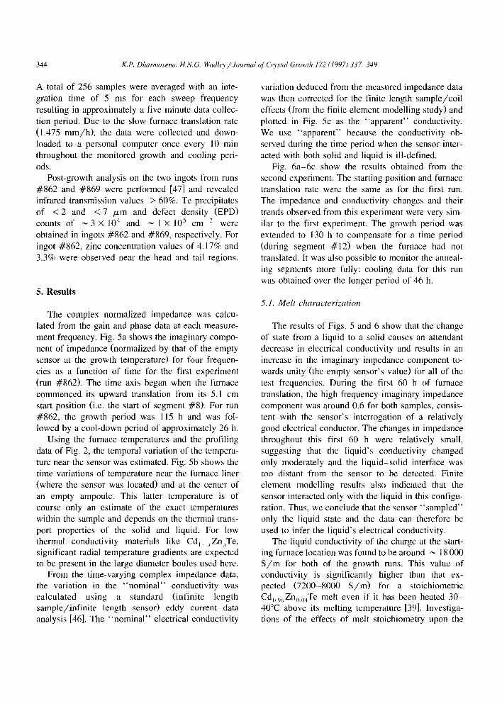
Fig. 5. (a) Measured impedance response at four frequencies for run #862 during crystal growth and cooling. (b) Furnace temperature variation during crystal growth and cooling. (c) The "apparent" conductivity variation during crystal growth and cooling.
A total of 256 samples were averaged with an inte- gration time of 5 ms for each sweep frequency resulting in approximately a five minute data collec- tion period. Due to the slow furnace translation rate (1.475 ram/h), the data were collected and down- loaded to a personal computer once every 10 rain throughout the monitored growth and cooling peri- ods.
Post-growth analysis on the two ingots from runs #862 and #869 were performed [47] and revealed infrared transmission values > 60%. Te precipitates of < 2 and < 7 /.Lm and defect density (EPD) counts of ~ 3 × 10⁴ and ~ l × 105 cm 2 were obtained in ingots #862 and #869, respectively. For ingot #862, zinc concentration values of 4.17% and 3.3% were observed near the head and tail regions.
5. Results
The complex normalized impedance was calcu- lated from the gain and phase data at each measure- ment frequency. Fig. 5a shows the imaginary compo- nent of impedance (normalized by that of the empty sensor at the growth temperature) for four frequen- cies as a function of time for the first experiment (run #862). The time axis began when the furnace commenced its upward translation from its 5.1 cm start position (i.e. the start of segment #8). For run #862, the growth period was 115 h and was fol- lowed by a cool-down period of approximately 26 h.
Using the furnace temperatures and the profiling data of Fig. 2, the temporal variation of the tempera- ture near the sensor was estimated. Fig. 5b shows the time variations of temperature near the furnace liner (where the sensor was located) and at the center of an empty ampoule. This latter temperature is of course only an estimate of the exact temperatures within the sample and depends on the thermal trans- port properties of the solid and liquid. For low thermal conductivity materials like Cdi_~Zn.,Te, significant radial temperature gradients are expected to be present in the large diameter boules used here.
From the time-varying complex impedance data, the variation in the "nominal" conductivity was calculated using a standard (infinite length sample/infinite length sensor) eddy current data analysis [46]. The "nominal" electrical conductivity
variation deduced from the measured impedance data was then corrected for the finite length sample/coil effects (from the finite element modelling study) and plotted in Fig. 5c as the "apparent" conductivity. We use "apparent" because the conductivity ob- served during the time period when the sensor inter- acted with both solid and liquid is ill-defined.
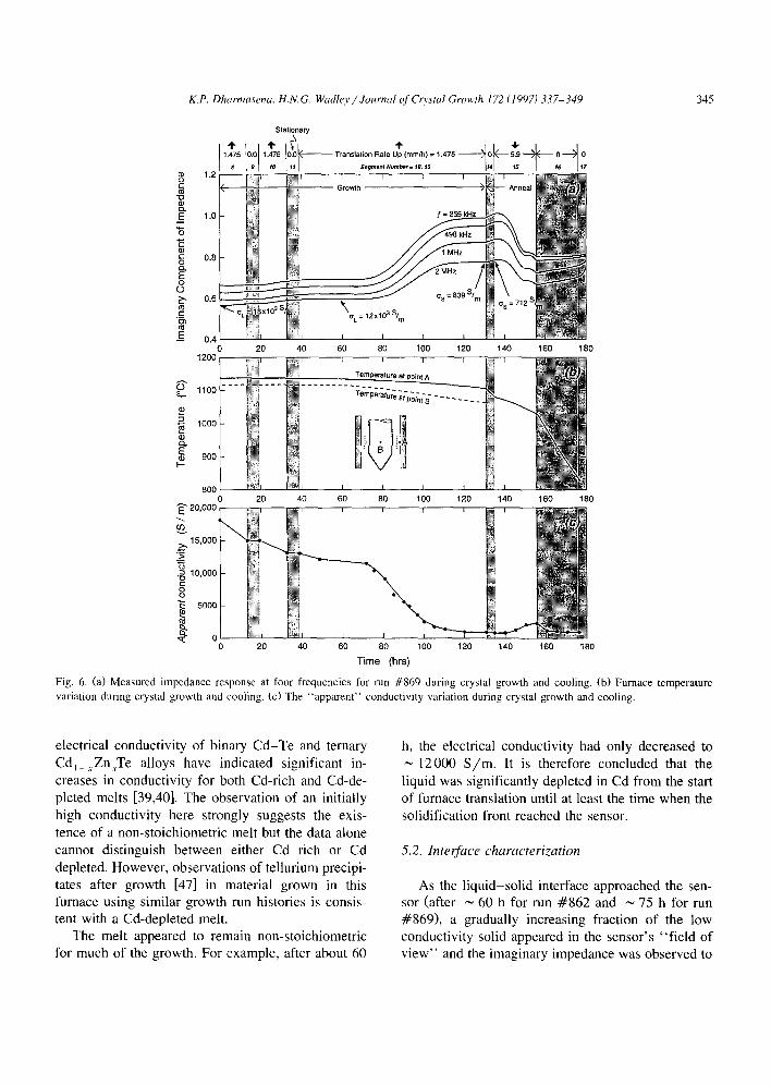
Fig. 6a-6c show the results obtained from the second experiment. The starting position and furnace translation rate were the same as for the first run. The impedance and conductivity changes and their trends observed from this experiment were very sim- ilar to the first experiment. The growth period was extended to 130 h to compensate for a time period (during segment #12) when the furnace had not translated. It was also possible to monitor the anneal- ing segments more fully; cooling data for this run was obtained over the longer period of 46 h.
5.1. Melt characterization
The results of Figs. 5 and 6 show that the change of state from a liquid to a solid causes an attendant decrease in electrical conductivity and results in an increase in the imaginary impedance component to- wards unity (the empty sensor's value) for all of the test frequencies. During the first 60 h of furnace translation, the high frequency imaginary impedance component was around 0.6 for both samples, consis- tent with the sensor's interrogation of a relatively good electrical conductor. The changes in impedance throughout this first 60 h were relatively small, suggesting that the liquid's conductivity changed only moderately and the liquid-solid interface was too distant from the sensor to be detected. Finite element modelling results also indicated that the sensor interacted only with the liquid in this configu- ration. Thus, we conclude that the sensor "sampled" only the liquid state and the data can therefore be used to infer the liquid's electrical conductivity.
The liquid conductivity of the charge at the start- ing furnace location was found to be around ~ 18 000 S / m for both of the growth runs. This value of conductivity is significantly higher than that ex- pected (7200-8000 S / m ) for a stoichiometric Cd0.96Zn0.04Te melt even if it has been heated 30- 40°C above its melting temperature [39]. Investiga- tions of the effects of melt stoichiometry upon the
K.P. Dha rmasena, H.N.G. Wadley / Journal of Crystal Growth 172 (1997) 337-349 345
Fig. 6. (a) Measured impedance response at four frequencies for run #869 during crystal growth and cooling. (b) Furnace temperature variation during crystal growth and cooling. (c) The "apparent" conductivity variation during crystal growth and cooling.
electrical conductivity of binary Cd-Te and ternary Cdj_~Zn~Te alloys have indicated significant in- creases in conductivity for both Cd-rich and Cd-de- pleted melts [39,40]• The observation of an initially high conductivity here strongly suggests the exis- tence of a non-stoichiometric melt but the data alone cannot distinguish between either Cd rich or Cd depleted. However, observations of tellurium precipi- tates after growth [47] in material grown in this furnace using similar growth run histories is consis- tent with a Cd-depleted melt.
The melt appeared to remain non-stoichiometric for much of the growth. For example, after about 60
h, the electrical conductivity had only decreased to ~ 12000 S/re . It is therefore concluded that the liquid was significantly depleted in Cd from the start of furnace translation until at least the time when the solidification front reached the sensor.
5.2. Interface characterization
As the liquid-solid interface approached the sen- sor (after ~ 6 0 h for run #862 and ~ 7 5 h f o r r u n #869), a gradually increasing fraction of the low conductivity solid appeared in the sensor's "field of view" and the imaginary impedance was observed to
rise for all of the frequencies measured, Figs. 5a and 6a. This was consistent with the behavior predicted using finite element modelling in which the greatest change of impedance occurs when the interface passes roughly through the center of the sensor [44]. The impedance data exhibited inflection points around 84 h after the start of furnace translation for run #862 and therefore roughly indicated the time of passage of the solid-liquid interface through the central region of the sensor. A time delay in the occurrence of the inflection point was observed in the second experiment (run #869). This was caused in part by the unintended time interval during which the furnace had not translated in segment #12. As a result, the interface appeared to have passed through the sensor after about 92 h (Fig. 6a). As the interface moved upwards away from the sensor, a decreasing fraction of the liquid and an increasing fraction of the solid were sampled, and the impedance ap- proached an asymptote determined by the conductiv- ity of the solid material.
The time at which the inflection point was ob- served has been predicted to depend on the interface location (relative to the sensor, h), its curvature (defined by a convexity parameter, 0 = Z/D, where Z is the axial displacement of the interface at the center relative to its position near the crucible wall, and D is the crucible diameter), and the test fre- quency [44]. The modelling study indicated that for intermediate frequencies, the time at which the in- flection point would be observed increases as the curvature changes from convex to flat, to concave. The modelling study revealed that the inflection points at higher frequencies became more indepen- dent of the interface shape and converged to a position that corresponded to near alignment of the outer edge of the interface with the sensor's mid- point. This phenomenon potentially enables the (in- terface shape independent) determination of the loca- tion and thus the growth rate of the interface. Once the time at which the interface was located at the center of the sensor was determined (h = 0), the relative large shifting of the inflection points at lower frequencies could then be used to estimate the shape of the interface (convex, concave or flat).
Fig. 7a and 7b show the frequency dependence of the inflection point time for runs #862 and #869, respectively. From the high frequency data, the time
80 - f - umace t r ans l a t i on ra te . . . . . . . . . . . . . . . . . .
7 0
6 0 i i i i r i J i ] i i i i i J i l l i b i i i , , i
10 105 106 10
Frequency (Hz)
Fig. 7. (a) Frequency dependence of the time appearance of the inflection point for run #862. (b) Frequency dependence of the time appearance of the inflection point for run #869.
at which the interface was located at the center of the sensor was found to be ~ 8 4 and ~ 9 2 h for run #862 and #869, respectively. If it is assumed that there is no delay in nucleation upon the start of translation, that the interface was flat, and that the movement of the interface (i.e. the growth rate) equalled the furnace translation rate, the time taken for the interface to reach the position of the sensor would be 66 h for the first experiment (run #862) and 81 h for the second (run #869). These are
significantly less than those measured (84 and 92 h respectively). The difference in the estimated and actual times could be due to (1) a growth rate not equal to the furnace translation rate, (2) a non-planar interface shape and (3) a delay in the onset of nucleation as a result of liquid supercooling. If the third possibility is discounted and we assume a shape with the convexity deduced below, the eddy current observed times for the passage of the interface through the sensor imply actual growth rates of 1.105 m m / h for the first experiment and 1.244 m m / h for the second. In previous experimental work with CdTe, growth rates of less than 35% of the translation rate have been reported [48]. The rates of 1.105 and 1.244 m m / h are less than the furnace translation rate (1.475 ram/h) and so solidification occurred lower in the furnace than anticipated.
Having determined the moment when the inter- face was located at the sensor's center, it is possible to use the result from the previous modelling study [44], to determine the interfacial curvature. Fig. 8 plots the position of the inflection point (relative to the interface location) against frequency for the two experiments, compared with the calculations done for the three interfaces in the modelling study [44]. It is apparent from this data that the interface curvature lay between the convex and flat cases modelled. The low frequency data for both growth runs was similar
15.0
1 0 0
8 = - 0 .333
~ 5.0
0.0
9 = 0 . 0
- 5 . 0 - o.
~" 8 = + 0 . 3 3 3 ~10~0
. . . . . . . . J . . . . . . . . I
Run #869
Run #862
-0.333 ! "So[~d I
- 1 5 . 0 ~ 10 10 5 10 6 10 7
F r e q u e n c y ( H z )
Fig. 8. Comparisons of experimental and calculated variations of the inflection point position with frequency.
indicating a convexity of about 0.167. Small differ- ences in the high frequency (small skin depth) eddy current behavior of the samples are indicative of a greater flattening of the interface near the ampoule wall for run #869. The recovery of a more exact shape of the interface requires a detailed multifre- quency inverse analysis of the impedance data.
Previous modelling work has shown that for ma- terial systems with liquid : solid thermal conductivity ratios (kJk~) greater than one, the interface shape is concave in the presence of a uniform temperature gradient. However, the interface could be made con- vex by reducing the temperature gradient above the interface and/or increasing the temperature gradient below the interface [48-50]. Evidence here of a non-stoichiometric melt suggests solidification oc- curs at a lower temperature than the 1099-1100°C associated with the liquidus of stoichiometric Cdo.095Zn0.045Te. The drop in melt temperature must move the interface upwards within the furnace into the region of shallower temperature gradients and therefore tends to make the interface more convex [51,52]. The lower than expected solidification tem- perature and the convex interface shape should have resulted in the interface moving past the sensor sooner than was assumed in our initial estimation of the growth rate (based on a flat interface propagating at the furnace translation rate). However, the multi- frequency inflection point analysis, Fig. 7, indicated a longer than expected time for the interface to reach the sensor. The most likely explanation for this is an initial delay in the onset of nucleation associated with liquid supercooling. An eddy current sensor placed at the ampoule tip could resolve this impor- tant issue [53].
5.3. Solid state annealing/cooling
Proper post-growth annealing/cooling assists in the homogenization of the Zn distribution and con- trols the dislocation density and the concentration of Te precipitates. The dislocation density and number of precipitates in a grown boule are affected by the cooling rate and the overall cooling period. During cool down, the impedance data collected from the eddy current sensor can be used to evaluate the conductivity of the cooling crystal and assess its potential for characterizing some aspects of post- growth phenomena.
For the first experiment, a solid conductivity of 923 S / m was observed at the end of growth (seg- ment #13), which further decreased to 791 S / m during a four hour stationary furnace segment (# 14) when the furnace zone temperatures in zones 2 through 4 were reduced by approximately 48°C. In the next segment (#15), the furnace was moved down to an annealing position, while the tempera- tures in zones 2 through 5 were decreased further by approximately 53°C. During these two segments, the temperatures in zones 1, 5 and 6 were maintained at 825, 1020 and 800°C, respectively. Data analyzed from the second experiment (run #869) revealed similar results. In this case, a post-growth conductiv- ity of 839 S / m was observed, which decreased to 712 S / m during the initial four hour cooling period (segment # 14).
An anomalous increase in sample conductivity has been detected during segment #15 when the furnace was moved to its annealing position. In conductivity experiments performed with samples having different Zn contents in a quasi-steady state furnace, a slight anomalous increase in conductivity after solidification was initially detected (i.e. within 40°C of solidification) for Cd0.%Zn0.04Te and was then followed by a gradual decrease in conductivity with temperature during the remaining cool down [39]. Modelling studies of the Zn segregation has revealed concentrations varying from ~ 5.8% (near the first to freeze region) to 2.8% (near the top of the boule) [25]. One possible explanation for the rise in conductivity during post-growth cool down is the homogenization of Zn by diffusion, which results in a more uniform concentration closer to 4% with an increased conductivity. In run #869, with the fur- nace stationary, segment #16 allowed a controlled furnace cool down to 825°C during which time a gradual decrease in conductivity was observed con- sistent with the decrease in temperature.
6. Summary
Detailed experiments have been conducted with an eddy current sensor in a vertical Bridgman fur- nace to better understand the CdZnTe growth pro- cess and to obtain information about the solid-liquid interface. From the measured impedance data, the
sensor has demonstrated the capability of providing significant new information about the melt composi- tion and has revealed that growth occurred from a non-stoichiometric (probably) Cd-depleted melt. An analysis of the high frequency data has enabled the interface's location to be deduced and has revealed that the growth rates were lower than the furnace translation rate so that solidification occurred in a colder section of the furnace where the temperature gradient was steeper than anticipated. Lower fre- quency data revealed that growth occurred with a less than ideal convex interface shape. Post-growth monitoring of the cooling process has enabled the electrical conductivity data of the solid to be moni- tored. An "anomalous" increase in conductivity was observed as the temperature was decreased from the solidification temperature.
Acknowledgements
This work has been performed as a part of the research of the Infrared Materials Producibility Pro- gram conducted by a consortium that includes John- son Matthey Electronics, Texas Instruments, I I -VI Inc., Loral, the University of Minnesota and the University of Virginia. We are grateful for the many helpful discussions with our colleagues in these or- ganizations. We would also like to thank Art Socha of Johnson Matthey Electronics for providing data from the post-growth characterization of the ingots. The consortium work has been supported by ARPA/CMO under contract MDA972-91-C-0046 monitored by Raymond Balcerak.
References
[1] S. Sen and J.E. Stannard, Mater. Res. Soc. Symp. Proc. 302 (1993) 391.
[2] W.E. Tennant, C.A. Cockrum, J.B. Gilpin, M.A. Kinch, M.B. Reine and R.P. Ruth, J. Vac. Sci. Technol. B 10 (1992) 1359.
[12] S. Sen, W.H. Konkel, S.J. Tighe, L.G. Bland, S.R. Sharma and R.E. Taylor, J. Crystal Growth 86 (1988) 111.
[13] P. Brunet, A. Katty, D. Schneider, A. Tromson-Carli and R. Triboulet, Mater. Sci. Eng. B 16 (1993) 44.
[14] P. Cheuvart, U. El-Hanani, D. Schneider and R. Triboulet, J. Crystal Growth 101 (1990) 270.
[15] K.Y. Lay, D. Nichols, S. McDevitt, B.E. Dean and C.J. Johnson, J. Crystal Growth 86 (1988) 118.
[16] A.A. Khan, W.P. Allred, B. Dean, S. Hooper, J.E. Hawkey and C.J. Johnson, J. Electron. Mater. 15 (1986) 181.
[17] A. Socha, personal communication, 1993. [18] C.K. Ard, personal communication, 1993. [19] P.-K. Liao, personal communication, 1993. [20] P. Capper, J.E. Harris, E.S. O'Keefe and C.L. Jones, Adv.
Neugebauer and H.F. Schaake, J. Electron. Mater. 24 (1995) 505.
[22] A.B. Bollong, P.W. Norton, H.F. Schaake, C.K. Ard, N. Wereley and H.N.G. Wadley, Proc. IRIS Specialty Group on Infrared Materials, Moffet Field, CA, 1992.
[23] M. Pfeiffer and M. Muhlberg, J. Crystal Growth 118 (1992) 269.
[24] S. Kuppurao, S. Brandon and J.J. Derby, J. Crystal Growth 155 (1995) 93.
[25] S. Kuppurao, S. Brandon and J.J. Derby, J. Crystal Growth 155 (1995) 102.
[26] S. Kuppurao, S. Brandon and J.J. Derby, J. Crystal Growth 158 (1996) 459.
[27] Q. Xiao, S. Kuppurao and J.J. Derby, J. Crystal Growth 167 (1996) 292.
[28] H.F. Schaake, personal communication, 1993. [29] D.J. Larson, R.P. Silberstein, D. DiMarzio, F.C. Carlson, D.
Gillies, G. Long, M. Dudley and J. Wu, Semicond. Sci. Technol. 8 (1993) 911.
[30] H.N.G. Wadley and W.E. Eckhart, Jr., J. Metals, Oct. (1989) 10.
[31] H.S. Goldberg, in: Proc. Syrup. Intelligent Processing of Materials, Eds. H.N.G. Wadley and W.E. Eckhart, Jr. (1990) p. 83.
[32] D.E. Witter, in: Proc. Symp. Intelligent Processing of Materi- als, Eds. H.N.G. Wadley and W.E. Eckhart, Jr. (1990) p. 91.
[33] H.N.G. Wadley and K.P. Dharmasena, J. Crystal Growth 130 (1993) 553.