EDUCATIONAL APPLICATIONS OF PARTIAL RECONFIGURATION OF FPGAS By Maysam Sarfaraz A Thesis Submitted to the Faculty of the University of Tennessee at Chattanooga in Partial Fulfillment of the Requirements for the Degree of Master of Science in Electrical Engineering The University of Tennessee at Chattanooga Chattanooga, Tennessee May 2011
Transcript
EDUCATIONAL APPLICATIONS OF PARTIAL RECONFIGURATION
OF FPGAS
By
Maysam Sarfaraz
A Thesis Submitted to the Faculty of the
University of Tennessee at Chattanooga in Partial Fulfillment of the Requirements
for the Degree of Master of Science in Electrical Engineering
The University of Tennessee at Chattanooga Chattanooga, Tennessee
May 2011
ii
To the Graduate Council: I am submitting herewith a thesis written by Maysam Sarfaraz entitled “Educational Applications of Partial Reconfiguration of FPGAs” I have examined the final electronic copy of this thesis for form and content and recommend that it be accepted in partial fulfillment of the requirements for the degree of Master of Science, with a major in Electrical Engineering.
Dr. Stephen Craven
Major Professor We have read this thesis and recommend its acceptance:
Dr. Ahmed Eltom Dr. Raziq Yaqub Accepted for the Council:
Dr. Jerald Ainsworth Dean of the Graduate School
(Original Signatures are on file with official student records.)
iii
ABSTRACT The use of partial reconfiguration (PR) in reconfigurable systems such as Field
Programming Gate Arrays (FPGAs) has gained a lot of attention during the past ten
years. Recently, Xilinx has released the first commercially available PR implementation
for its FPGAs. However, there is a lack of educational tools for PR instruction. In
addition, the design and implantation of PR on FPGAs can be beneficial compared with
the current communications tools within academia. This thesis presents the design and
simulation of several basic modulation schemes within Simulink and System Generator
for educational applications in communications classes. In addition, the implementation
process of creating and testing additional partial bitstreams will take a few minutes rather
than a few hours, which make this reconfigurable system a suitable system for
educational applications. Furthermore, each modulation scheme can be implemented
without any use of Hardware Description Language (HDL), embedded, and software
development design. After implementing these models on an FPGA the results of these
implementations are analyzed and compared with the simulation results. The results
demonstrate the proper implementation of these PR designs on FPGAs.
iv
ACKNOWLEDGEMENTS
This thesis was written under the direction and supervision of Dr. Stephen
Craven. I would personally like to thank Dr. Stephen Craven as my advisor for his
patient guidance throughout the course of my thesis at the University of Tennessee at
Chattanooga. My appreciations also go to the committee members of this thesis, Dr.
Ahmed Eltom and Dr. Raziq Yaqub.
v
TABLE OF COTETS
ABSTRACT....................................................................................................................... iii
ACKNOWLEDGEMENT ................................................................................................. iv
TABLE OF CONTENTS.....................................................................................................v
LIST OF TABLES.............................................................................................................vii
LIST OF FIGURES...........................................................................................................viii
LIST OF ABBREVIATIONS............................................................................................ xi
CHAPTER
I. INTRODUCTION............................................................................................... 1
Advantages of Reconfigurable Systems.............................................................. 1 Advantages of Partial Reconfiguration ............................................................... 2 Existing Educational and Research Projects ....................................................... 3 Thesis Goals and Objectives ............................................................................... 4 Thesis Overview.................................................................................................. 5
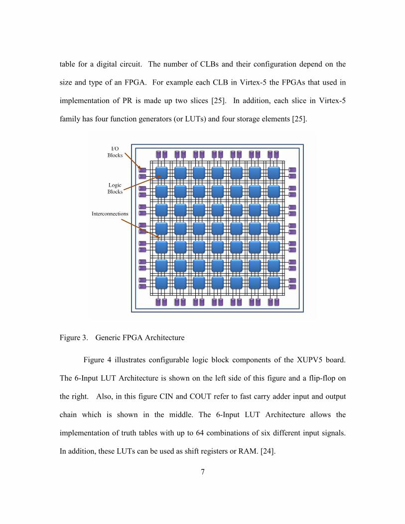
II. BACKGROUND................................................................................................. 6
FPGA Architecture and Technology................................................................... 6 Partial Reconfigurations in FPGAs ..................................................................... 8 FPGA Design Tools ............................................................................................ 9
III. DESIGNS AND METHODS ............................................................................ 11
Modulation in Communication Systems ........................................................... 11 Simulation within Matlab / Simulink ................................................................ 13 System Generator Design Process..................................................................... 23
IV. RESULTS AND DISCUSSION........................................................................ 27
Partial Reconfiguration Implementation Process .............................................. 29 Results of PR Implementation on the FPGA .................................................... 34
vi
V. CONCLUSIONS AND RECOMMENDATIONS............................................ 45
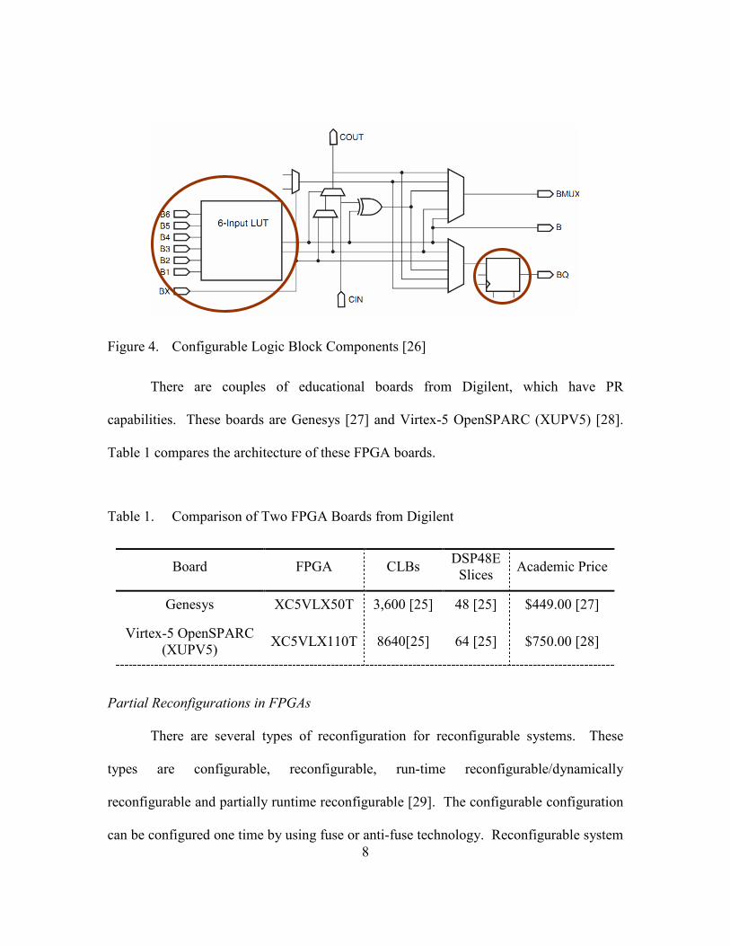
Figure 5. AM Demodulator using an Envelope Detector in the Time Domain (right) and its Circuit Configuration (left) ............................................................. 13
Figure 6. Block Diagram of Coherent Detector or Synchronous Demodulator ......... 14
Figure 7. AM Modulation and Demodulation within Simulink ................................. 15
Figure 8. Simulation Results of AM Modulation in Simulink (a) Input Sine Signal (b) Method 1 Modulation (c) Method 2 Modulation ........................................ 16
Figure 9. Simulation Results of AM Modulation in Simulink (a) Method 1 Demodulation (b) Method 2 Demodulation (c) Method 3 Demodulation (d) Method 1 Demodulation.............................................................................. 16
Figure 10. AM Modulation and Demodulation of an Audio Signal in Simulink ......... 17
Figure 11. Simulation Results of AM Modulation of an Audio Signal in Simulink (a) Input Audio Signal (b) Audio Signal after Modulation (c) Recovered Audio Signal after Demodulation........................................................................... 18
Figure 12. Frequency Spectrum of an Audio Signal after Modulation (a) and Demodulation (b) for AM Modulation........................................................ 18
Figure 13. DSB-SC Modulation and Demodulation within Simulink.......................... 19
Figure 14. Simulation Results of DSB-SC Modulation in Simulink (a) Input Sine Signal (b) Method 1 Modulation (c) Method 2 Modulation ....................... 20
Figure 16. DSB-SC Modulation and Demodulation of an Audio Signal in Simulink 21
Figure 17. Simulation Results of DSB-SC Modulation of an Audio Signal in Simulink (a) Input Audio Signal (b) Audio Signal after Modulation (c) Recovered Audio Signal after Demodulation................................................................ 22
Figure 18. Frequency Spectrum of an Audio Signal after Modulation (a) and Demodulation (b) for DSB-SC.................................................................... 22
Figure 19. AM Modulation and Demodulation of a Sine Wave in System Generator 24
Figure 20. Simulation Results of AM Modulation in System Generator (a) Input Sine Signal (b) Signal after Modulation (c) Recovered Signal after Demodulation 24
Figure 21. DSB-SC Modulation and Demodulation of a Sine Wave in System Generator ..................................................................................................... 25
Figure 22. Simulation Results of DSB-SC Modulation in System Generator (a) Input Sine Signal (b) Signal after Modulation (c) Recovered Signal after Demodulation .............................................................................................. 25
Figure 23. Representation of PR Implementation on Virtex-5 (XUPV5) Board ......... 28
Figure 24. Defining the Reconfigurable Regions ......................................................... 32
Figure 25. Process of Changing Partial Bits through HyperTerminal.......................... 34
Figure 27. DSB-SC Modulation Process ...................................................................... 36
Figure 28. Input Signal and Output Results of Modulated Signal (DSB-SC Modulation) on the FPGA (1) Input Signal (2) Output Signal.................... 36
Figure 29. Output Results of Modulated Signal (DSB-SC Modulation) on the FPGA (a) 200ms Sec/Div (b) 5ms Sec/Div............................................................ 37
Figure 30. AM Modulation Block Diagram in System Generator ............................... 38
Figure 31. Output Results of Modulated Signal (AM Modulation) on the FPGA (1) Input Signal (2) Output Signal .................................................................... 38
Figure 32. Output Results of Modulated Signal (AM Modulation) on the FPGA (1) Input Audio Signal (2) Output Audio Signal .............................................. 39
x
Figure 33. Entire DSB-SC Modulation and Demodulation on a Same Module.......... 40
Figure 34. Output Results of DSB-SC Modulation on the FPGA (1) Input Signal (2) Output Signal............................................................................................... 40
Figure 35. Output Results of DSB-SC Modulation on the FPGA (1) Input Audio Signal (2) Output Audio Signal .............................................................................. 41
Figure 36. Entire AM Modulation and Demodulation on a Same RP......................... 41
Figure 37. Output Result of AM Modulation on the FPGA (1) Input Signal (2) Output Signal........................................................................................................... 42
Figure 38. Output Result of AM Modulation on the FPGA (1) Input Signal (2) Output Signal........................................................................................................... 43
Figure 39. DSB-SC Demodulator (Radio Receiver) in System Generator ................. 43
Figure 40. Output Result of DSB-SC Demodulation on the FPGA (1) Input Signal (2) Output Signal............................................................................................... 44
Figure 41. Output Result of DSB-SC Demodulation on the FPGA (1) Input Audio Signal (2) Output Audio Signal................................................................... 44
xi
LIST OF ABBREVIATIOS
AM Amplitude Modulation ASIC Application-specific integrated circuit BEE Berkeley Emulation Engine CLB Configurable Logic Block CPLD Complex Programmable Logic Device CPU Central processing units
DSB-SC Double SideBand-Suppressed Carrier DSP Digital Signal Processing EDK Embedded Development Kit FM Frequency Modulation FPGA Field Programming Gate Array
HDL Hardware Description Language
IC Integrated Circuit
ICAP Internal Configuration Access Port
LAB Logic Array Blocks
MATLAB Matrix Laboratory
OSSIE Open-Source SCA Implementation Embedded
PM Phase Modulation
xii
PR Partial Reconfiguration
RP Reconfigurable Partition
SCA Software Communications Architecture
SDR Software Defined Radio
SDK Software Development Kit
WARP Wireless Open Access Research Platform
XST Xilinx Synthesis Technology
1
CHAPTER I
ITRODUCTIO
Nowadays, reconfigurable systems such as Field Programming Gate Arrays
(FPGAs) are becoming popular for different applications in areas such as defense,
automotive, broadcasting, high performance computing and data storage, wired
communications, wireless communication, etc. This fact provides great opportunities for
research and educational communities to enhance and create more efficient ways to
leverage the use of these reconfigurable devices. One of the capabilities of these systems
is partial reconfiguration (PR) in which allow designers to overcome lack of resources of
FPGAs. This thesis looks into the advantages of partial reconfiguration capabilities of
FPGAs and leverages its usage in educational and research applications.
Advantages of Reconfigurable Systems
There are several reconfigurable systems in the market. FPGAs are the most
common reconfigurable systems that used among all other reconfigurable systems. The
FPGAs usually are compared to Application-Specific Integrated Circuits (ASICs). ASIC
is an Integrated Circuit (IC) for a specific purpose, and its hardware configuration cannot
change after its production. They are more expensive to design compared with FPGAs.
However, they can operate at higher frequencies with lower power consumption
compared with FPGAs.
2
FPGAs give an opportunity to the user to change the hardware reconfiguration
unlike the ASIC. This capability can avoid series of delays due to hardware conflicts [1].
For example, an operation can be delayed due to lack of certain hardware resources such
as DSP block in an ASIC. Moreover, this reconfigurable capability made these devices
an ideal tool for teaching digital design in academia. In addition, FPGAs have a fast and
cheap implementation time versus ASIC designs.
There are several companies that produce FPGAs in the market. Some of these
companies are Xilinx [2], Altera [3], Lattice [4], Actel [5]. In addition, several
educational and evaluation kits are available from different vendors such as Avnet [6]
and Digilent [7] for Xilinx FPGAs.
Advantages of Partial Reconfiguration
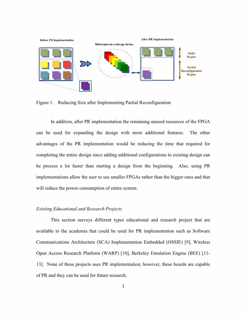
Partial reconfiguration helps to reduce cost and board space, providing a
flexibility to change a portion of the system dynamically without shutting down the entire
system [8]. Figure 1 illustrates how the use of PR will reduce the implementation size of
the design on the FPGAs. This figure illustrates an FPGA with a design that three
partitions of that are dedicated for static regions and the rest of the FPGA can be used for
PR implementation. The left portion of this figure shows this FPGA without PR
implementation. This portion can hold only few different designs within partial
reconfiguration region of the FPGA. However, after PR implementation (right portion of
the figure) a lot of additional designs can be stored outside of the FPGA and swapped if
there is need for change during operation of the FPGA.
3
Figure 1. Reducing Size after Implementing Partial Reconfiguration
In addition, after PR implementation the remaining unused resources of the FPGA
can be used for expanding the design with more additional features. The other
advantages of the PR implementation would be reducing the time that required for
completing the entire design since adding additional configurations to existing design can
be process a lot faster than starting a design from the beginning. Also, using PR
implementations allow the user to use smaller FPGAs rather than the bigger ones and that
will reduce the power consumption of entire system.
Existing Educational and Research Projects
This section surveys different types educational and research project that are
available to the academia that could be used for PR implementation such as Software
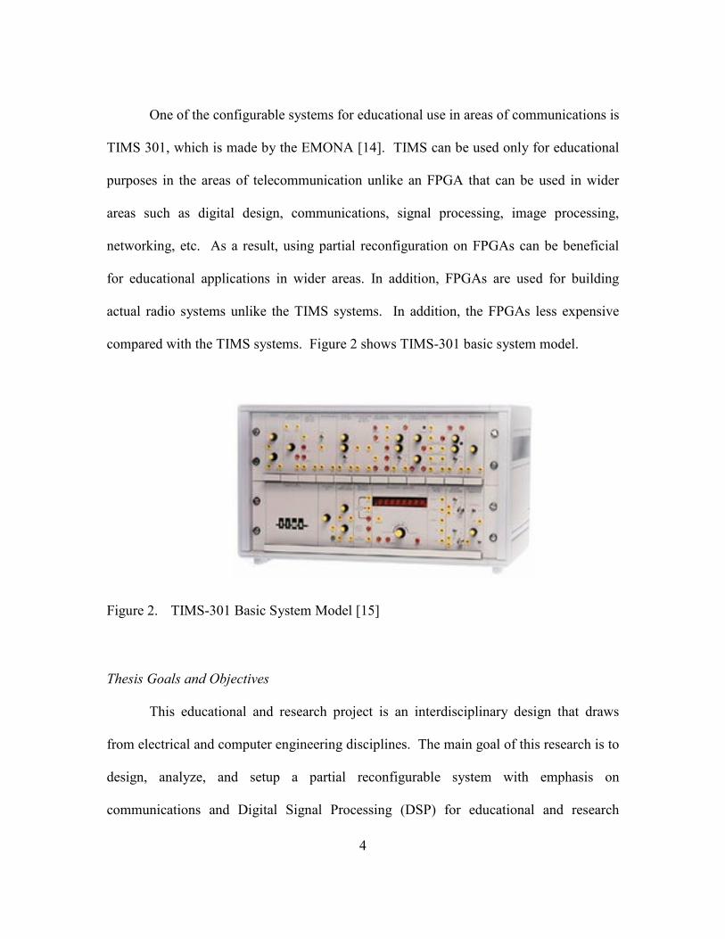
There are couples of educational boards from Digilent, which have PR
capabilities. These boards are Genesys [27] and Virtex-5 OpenSPARC (XUPV5) [28].
Table 1 compares the architecture of these FPGA boards.
Table 1. Comparison of Two FPGA Boards from Digilent
Board FPGA CLBs DSP48E
Slices Academic Price
Genesys XC5VLX50T 3,600 [25] 48 [25] $449.00 [27]
Virtex-5 OpenSPARC (XUPV5)
XC5VLX110T 8640[25] 64 [25] $750.00 [28]
Partial Reconfigurations in FPGAs
There are several types of reconfiguration for reconfigurable systems. These
types are configurable, reconfigurable, run-time reconfigurable/dynamically
reconfigurable and partially runtime reconfigurable [29]. The configurable configuration
can be configured one time by using fuse or anti-fuse technology. Reconfigurable system
9
can be erasing and programmed over and over. Run-time reconfigurable on other hand,
allows the reconfiguration of the system during its operation [29]. Finally, the partial
reconfiguration allows reconfiguration of portion of hardware while the static part is
operational [29]. PR can be used in wide variety of applications such as image
processing, Software Define Radio (SDR), encryption, etc.
The concept of partial reconfiguration in reconfigurable system has gained a lot of
attentions within academia during past few years. However, the partial reconfiguration
never been used for educational applications. Xilinx recently released the first
commercially available PR implantation for its FPGAs [8]. This implementation
supported for Virtex-4, Virtex-5, and Virtex-6 FPGAs. In addition, Xilinx has several
tutorials for this PR implementation [30]. However, at this point these tutorials are not
covering a detail PR implementation in the area of communications. Using partial
reconfiguration in communications classes allow the user to design, build, implement,
and test communication modules in a few minutes rather than a few hours on an FPGA.
FPGA Design Tools
The current version of Xilinx ISE design suite tools is version 13.1 [31]. The ISE
consists of several tools such as PlanAhead [32] for design analysis, ISE project manager
as a Synthesizer, ISim [33] as a simulator, Embedded Development Kit (EDK) [34], [35]
for embedded designs, Software Development Kit (SDK) [34], [35] for software
applications targeting soft and embedded processors within FPGAs, System Generator
[36] for DSP applications, etc. In this section, the ISE design tools is discussed since the
10
Xilinx provided these tools to universities free of charge for educational and research
applications.
11
CHAPTER III
DESIGS AD METHODS
This chapter looks into several simulation results within Simulink and System
Generator. First, the theory behind some of the most common modulations such as AM
and Double SideBand-Suppressed Carrier (DSB-SC) modulations is presented. Next
these modulations were built and tested within Simulink. Next, the audio signal was
imported to the Simulink and the simulation result was analyzed before implementation
of the design within System Generator. Finally, these designs were implemented within
System Generator for educational applications.
Modulation in Communication Systems
Communications system can transmit and receive analog or digital signals.
Analog modulation can be characterized as Amplitude Modulation (AM), Frequency
Modulation (FM), or Phase Modulation (PM). In these modulations the information or
baseband signal will be attached to corresponding properties of carrier signal, for
example in AM modulation the information is attached to the carrier amplitude [37].
This section covers two modulation schemes. These modulations are AM and DSB-SC
modulations. First, AM modulation is discussed then looked into DSB-SC modulation for
educational applications. In order to analyze AM modulation first a message ( )m t and a
12
carrier wave ( )c t are defined. These waves are illustrated in Equation 1 [38]. In this
equation, mA is m message signal amplitude, cA is carrier signal amplitude, mf is
message signal frequency, and cf is carrier signal frequency.
( ) cos(2 )m mm t A f tπ= ,
( ) cos(2 )c cc t A f tπ= (1)
Now the AM modulated wave ( )s t is defined by [38]
( ) [1 ( )]cos(2 )c a cs t A k m t f tπ= + (2)
In Equation 2 the ak is called the amplitude sensitivity. In order to detect
envelope of modulated wave ( )s t properly and avoid envelope distortion the amplitude
of ( )ak m t should be less than one.
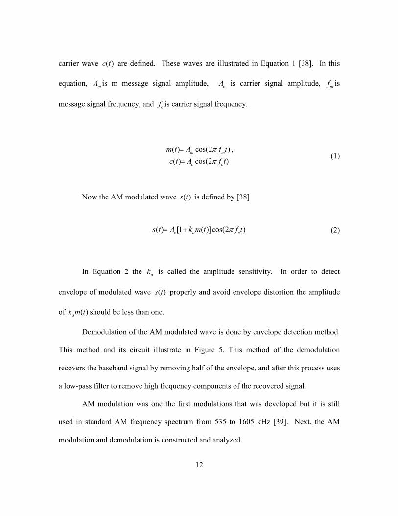
Demodulation of the AM modulated wave is done by envelope detection method.
This method and its circuit illustrate in Figure 5. This method of the demodulation
recovers the baseband signal by removing half of the envelope, and after this process uses
a low-pass filter to remove high frequency components of the recovered signal.
AM modulation was one the first modulations that was developed but it is still
used in standard AM frequency spectrum from 535 to 1605 kHz [39]. Next, the AM
modulation and demodulation is constructed and analyzed.
13
Figure 5. AM Demodulator using an Envelope Detector in the Time Domain (right) and its Circuit Configuration (left) [37]
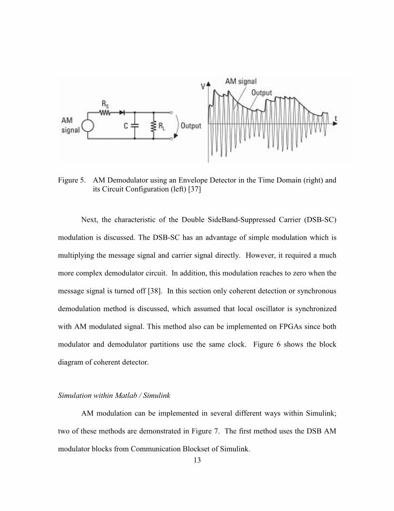
Next, the characteristic of the Double SideBand-Suppressed Carrier (DSB-SC)
modulation is discussed. The DSB-SC has an advantage of simple modulation which is
multiplying the message signal and carrier signal directly. However, it required a much
more complex demodulator circuit. In addition, this modulation reaches to zero when the
message signal is turned off [38]. In this section only coherent detection or synchronous
demodulation method is discussed, which assumed that local oscillator is synchronized
with AM modulated signal. This method also can be implemented on FPGAs since both
modulator and demodulator partitions use the same clock. Figure 6 shows the block
diagram of coherent detector.
Simulation within Matlab / Simulink
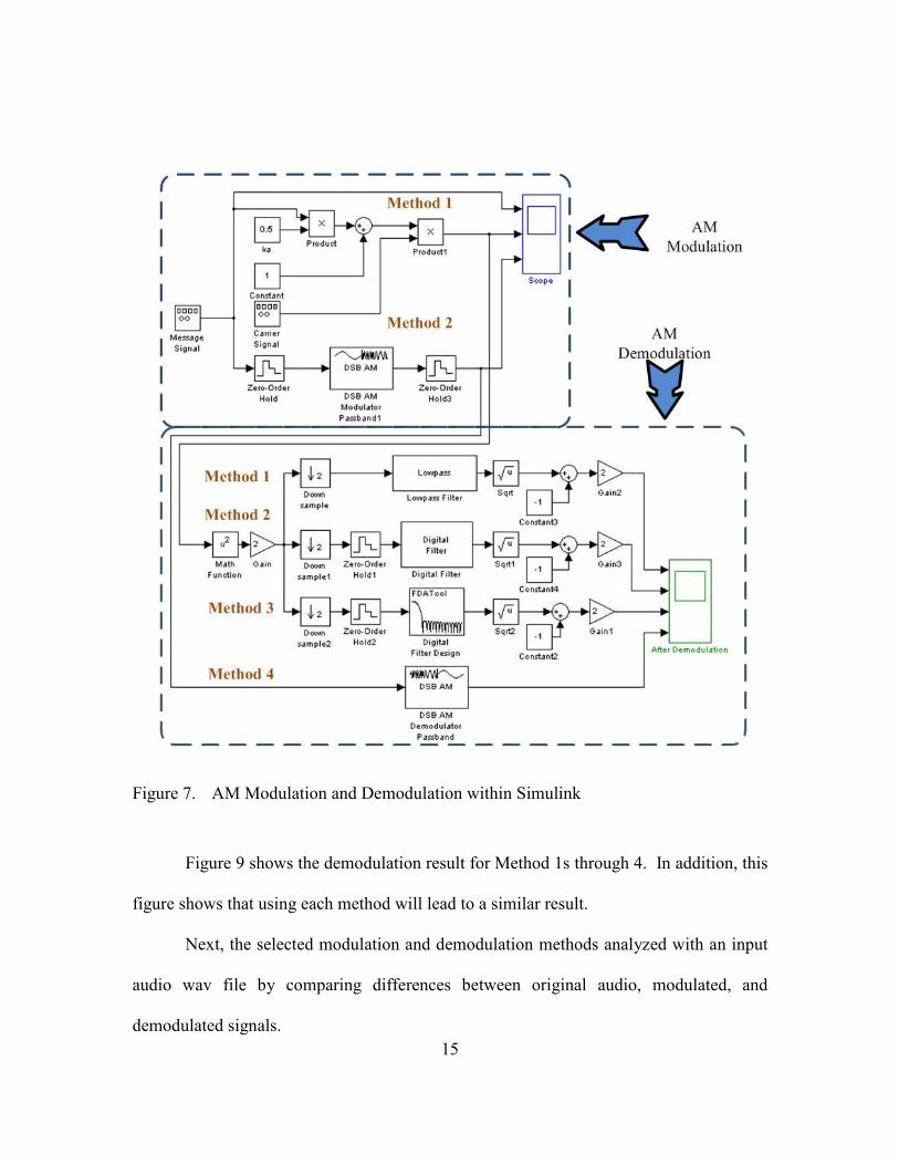
AM modulation can be implemented in several different ways within Simulink;
two of these methods are demonstrated in Figure 7. The first method uses the DSB AM
modulator blocks from Communication Blockset of Simulink.
14
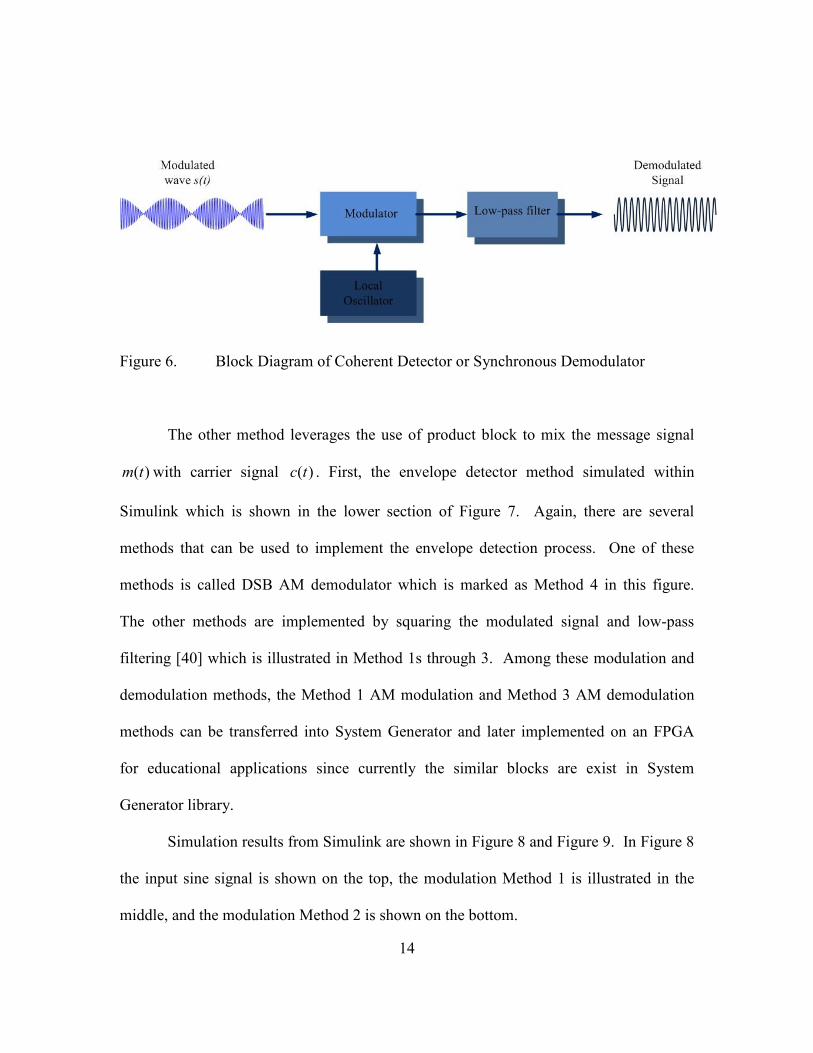
Figure 6. Block Diagram of Coherent Detector or Synchronous Demodulator
The other method leverages the use of product block to mix the message signal
( )m t with carrier signal ( )c t . First, the envelope detector method simulated within
Simulink which is shown in the lower section of Figure 7. Again, there are several
methods that can be used to implement the envelope detection process. One of these
methods is called DSB AM demodulator which is marked as Method 4 in this figure.
The other methods are implemented by squaring the modulated signal and low-pass
filtering [40] which is illustrated in Method 1s through 3. Among these modulation and
demodulation methods, the Method 1 AM modulation and Method 3 AM demodulation
methods can be transferred into System Generator and later implemented on an FPGA
for educational applications since currently the similar blocks are exist in System
Generator library.
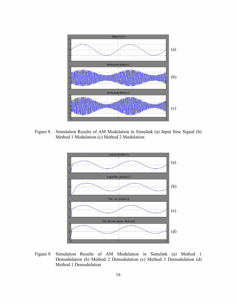
Simulation results from Simulink are shown in Figure 8 and Figure 9. In Figure 8
the input sine signal is shown on the top, the modulation Method 1 is illustrated in the
middle, and the modulation Method 2 is shown on the bottom.
15
Figure 7. AM Modulation and Demodulation within Simulink
Figure 9 shows the demodulation result for Method 1s through 4. In addition, this
figure shows that using each method will lead to a similar result.
Next, the selected modulation and demodulation methods analyzed with an input
audio wav file by comparing differences between original audio, modulated, and
demodulated signals.
16
Figure 8. Simulation Results of AM Modulation in Simulink (a) Input Sine Signal (b) Method 1 Modulation (c) Method 2 Modulation
Figure 9. Simulation Results of AM Modulation in Simulink (a) Method 1 Demodulation (b) Method 2 Demodulation (c) Method 3 Demodulation (d) Method 1 Demodulation
(a)
(b)
(c)
(d)
(a)
(b)
(c)
17
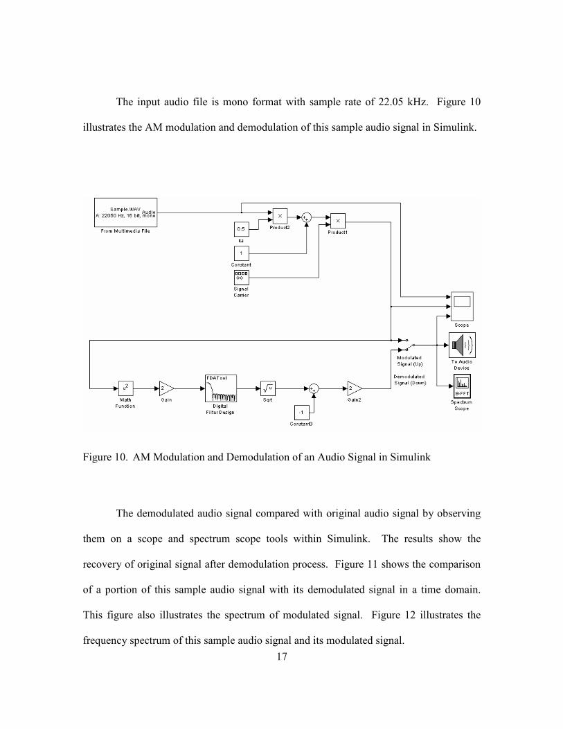
The input audio file is mono format with sample rate of 22.05 kHz. Figure 10
illustrates the AM modulation and demodulation of this sample audio signal in Simulink.
Figure 10. AM Modulation and Demodulation of an Audio Signal in Simulink
The demodulated audio signal compared with original audio signal by observing
them on a scope and spectrum scope tools within Simulink. The results show the
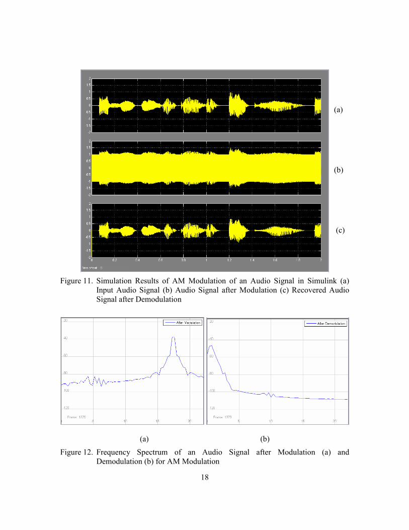
recovery of original signal after demodulation process. Figure 11 shows the comparison
of a portion of this sample audio signal with its demodulated signal in a time domain.
This figure also illustrates the spectrum of modulated signal. Figure 12 illustrates the
frequency spectrum of this sample audio signal and its modulated signal.
18
Figure 11. Simulation Results of AM Modulation of an Audio Signal in Simulink (a) Input Audio Signal (b) Audio Signal after Modulation (c) Recovered Audio Signal after Demodulation
(a) (b)
Figure 12. Frequency Spectrum of an Audio Signal after Modulation (a) and Demodulation (b) for AM Modulation
(a)
(b)
(c)
19
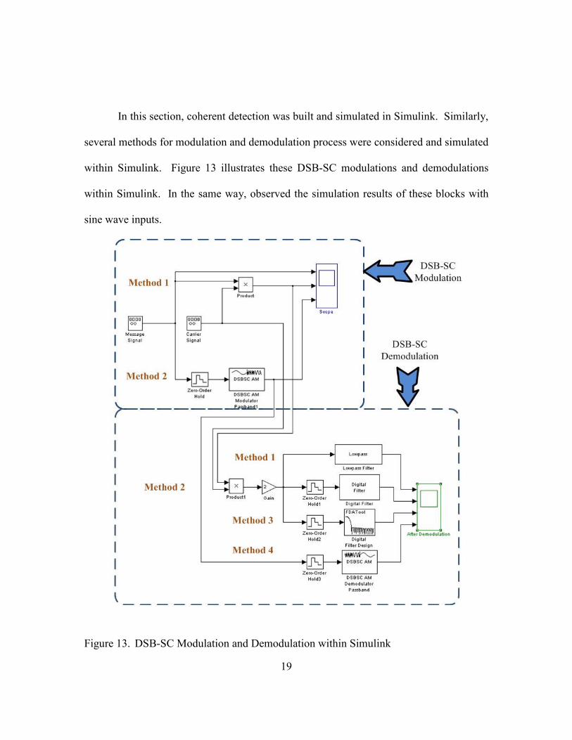
In this section, coherent detection was built and simulated in Simulink. Similarly,
several methods for modulation and demodulation process were considered and simulated
within Simulink. Figure 13 illustrates these DSB-SC modulations and demodulations
within Simulink. In the same way, observed the simulation results of these blocks with
sine wave inputs.
Figure 13. DSB-SC Modulation and Demodulation within Simulink
20
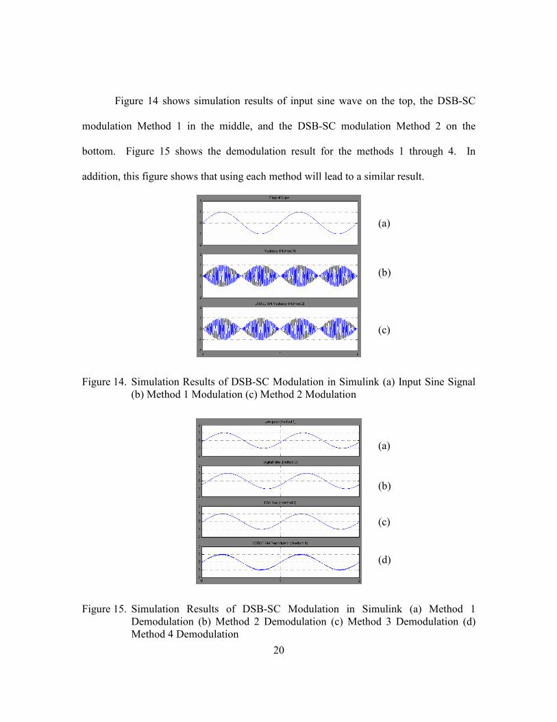
Figure 14 shows simulation results of input sine wave on the top, the DSB-SC
modulation Method 1 in the middle, and the DSB-SC modulation Method 2 on the
bottom. Figure 15 shows the demodulation result for the methods 1 through 4. In
addition, this figure shows that using each method will lead to a similar result.
Figure 14. Simulation Results of DSB-SC Modulation in Simulink (a) Input Sine Signal (b) Method 1 Modulation (c) Method 2 Modulation
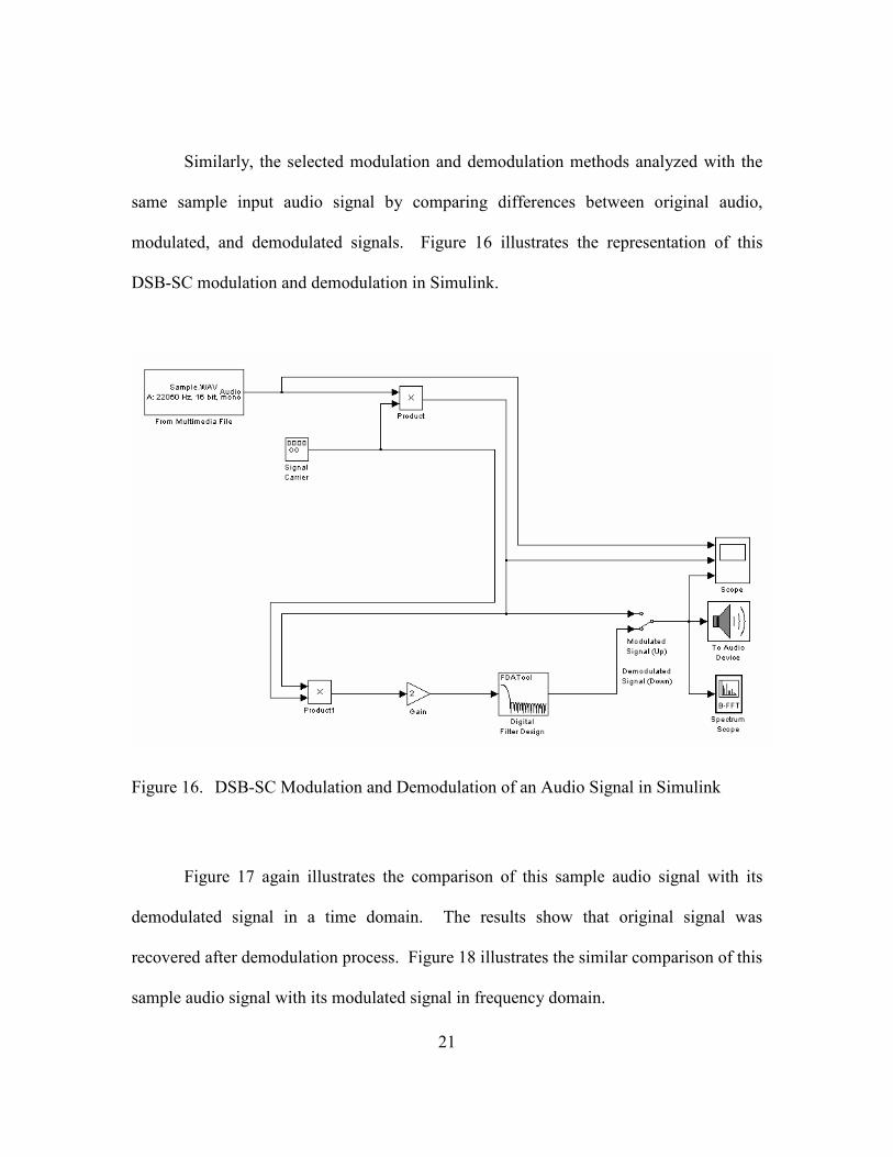
Similarly, the selected modulation and demodulation methods analyzed with the
same sample input audio signal by comparing differences between original audio,
modulated, and demodulated signals. Figure 16 illustrates the representation of this
DSB-SC modulation and demodulation in Simulink.
Figure 16. DSB-SC Modulation and Demodulation of an Audio Signal in Simulink
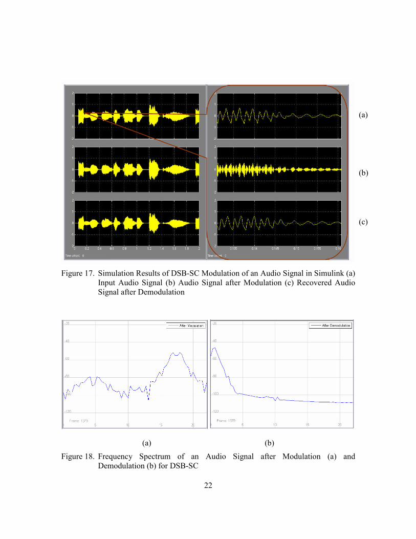
Figure 17 again illustrates the comparison of this sample audio signal with its
demodulated signal in a time domain. The results show that original signal was
recovered after demodulation process. Figure 18 illustrates the similar comparison of this
sample audio signal with its modulated signal in frequency domain.
22
Figure 17. Simulation Results of DSB-SC Modulation of an Audio Signal in Simulink (a) Input Audio Signal (b) Audio Signal after Modulation (c) Recovered Audio Signal after Demodulation
(a) (b)
Figure 18. Frequency Spectrum of an Audio Signal after Modulation (a) and Demodulation (b) for DSB-SC
(a)
(b)
(c)
23
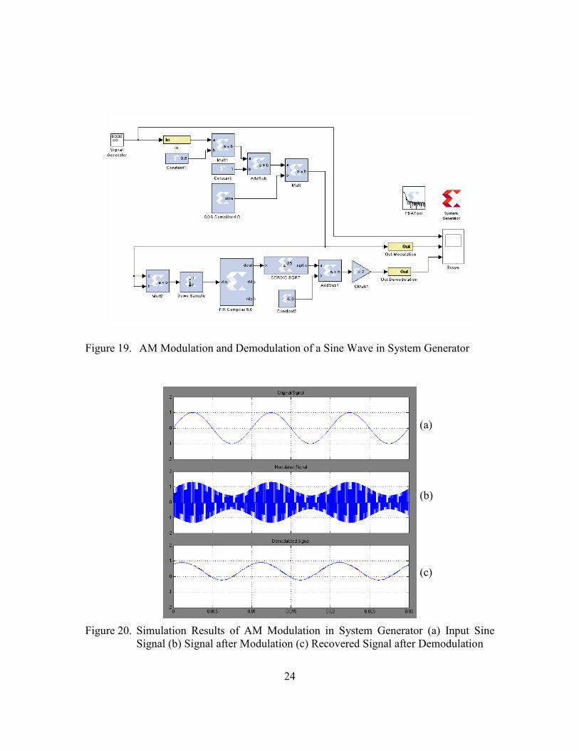
System Generator Design Process
This section covers the System Generator in details. System Generator is a useful
tool for designers with no back ground in Hardware Description Languages (HDLs).
This capability allows the designer to reduce design times, which is a suitable feature for
the educational applications. In this step the entire AM modulator using envelope
detector is built in System Generator which is shown in Figure 19. This figure shows that
System Generator uses two different types of blocks. Some of these blocks such as
Scope are directly imported to System Generator from Simulink and other blocks
provided by Xilinx.
In order to simulate the behavior of an FPGA the user should build each
modulation scheme within In and Out Xilinx blocks. System Generator does not provide
as many as blocks like Simulink; therefore, the designer must map his design from
Simulink modules to System Generator modules. For example System Generator does
not have Square block within its library; however, the user instead can use Mult Xilinx
block to get the square of a signal. The other Xilinx block that is used in this figure is
CORDIC SQRT which is similar to Sqrt block of Simulink which is shown in Figure 10.
Figure 20 shows System Generator simulation results of input sine wave on the
top, the AM modulation in the middle, and the recovered signal after demodulation
process on the bottom.
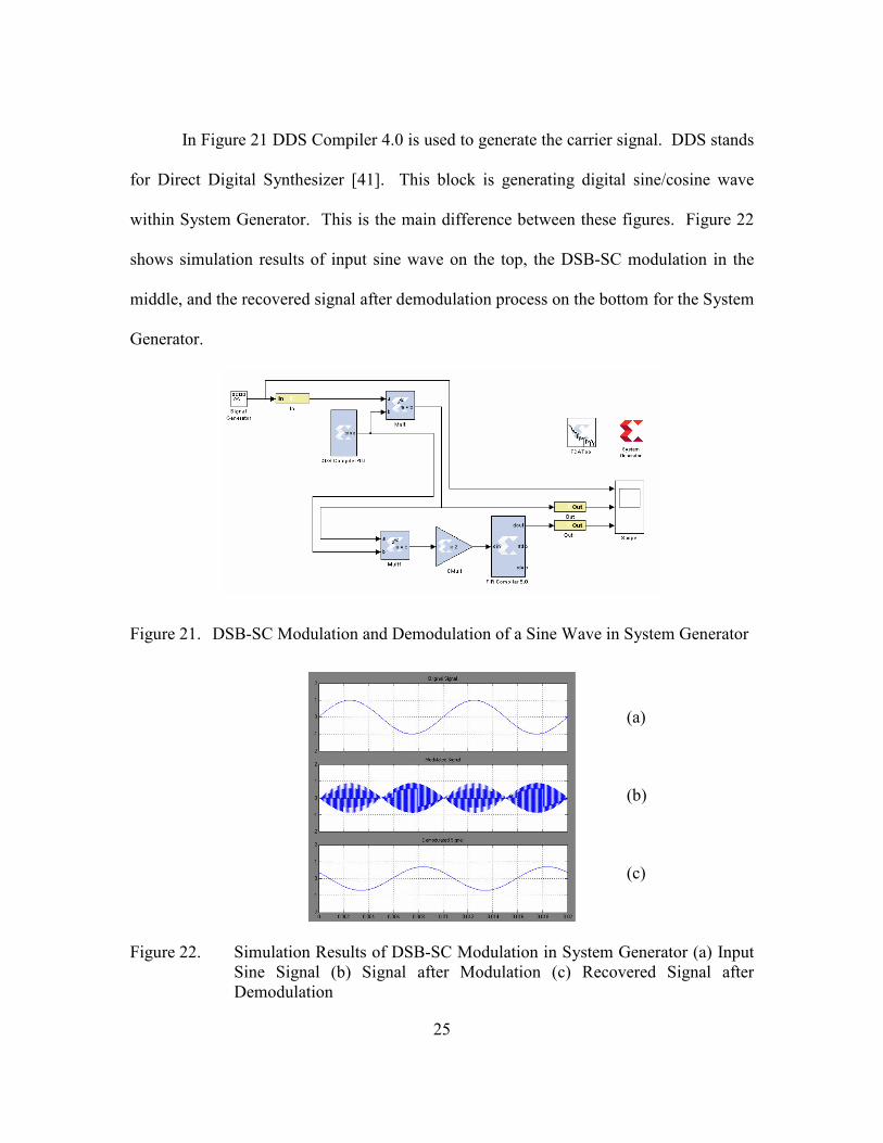
In the next step, the entire DSB-SC modulation is built in System Generator
which is shown in Figure 21. This figure has a lot of similarities to Figure 16 which is
showing the Simulink version of this modulation.
24
Figure 19. AM Modulation and Demodulation of a Sine Wave in System Generator
Figure 20. Simulation Results of AM Modulation in System Generator (a) Input Sine Signal (b) Signal after Modulation (c) Recovered Signal after Demodulation
(a)
(b)
(c)
25
In Figure 21 DDS Compiler 4.0 is used to generate the carrier signal. DDS stands
for Direct Digital Synthesizer [41]. This block is generating digital sine/cosine wave
within System Generator. This is the main difference between these figures. Figure 22
shows simulation results of input sine wave on the top, the DSB-SC modulation in the
middle, and the recovered signal after demodulation process on the bottom for the System
Generator.
Figure 21. DSB-SC Modulation and Demodulation of a Sine Wave in System Generator
Figure 22. Simulation Results of DSB-SC Modulation in System Generator (a) Input Sine Signal (b) Signal after Modulation (c) Recovered Signal after Demodulation
(a)
(b)
(c)
26
In the next chapter, these modules are implemented on an FPGA and the output of
the FPGA is tested and compared to the simulation results in System Generator and
Simulink.
27
Chapter IV
RESULTS AD DISCUSSIO
This chapter analyzes the performance of the implemented designs on an FPGA.
In addition, it describes how these designs were enhanced by modifying them. This
chapter shows that several design tools such as System Generator, and PlanAhead from
Xilinx are required at the same time in order to complete entire PR implementation
process. As mentioned earlier, System Generator is needed for designing and
implementing DSP and communications designs. This chapter first shows the process of
implementing partial reconfiguration through PlanAhead and finally validates the
successful PR implementation on XUPV5 board for educational applications in
communications classes.
In the previous chapters it was mentioned that Xilinx has several tutorials on
partial reconfigurations [30]. However, none of these tutorials address using of partial
reconfiguration for educational applications in communications classes. One of these
tutorials describes the implementation of PR of an audio filter on FPGAs. During the
process of PR implementation of a modulation and demodulation majority of the
embedded system design and parts of the software components were borrowed from
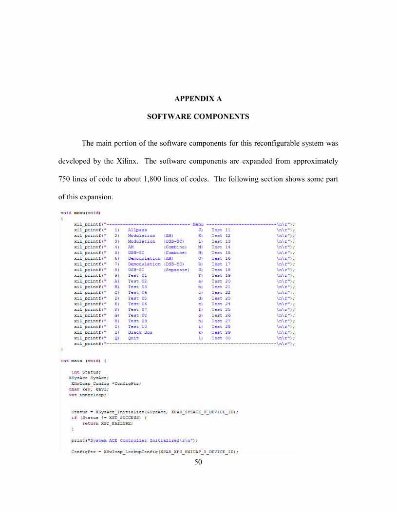
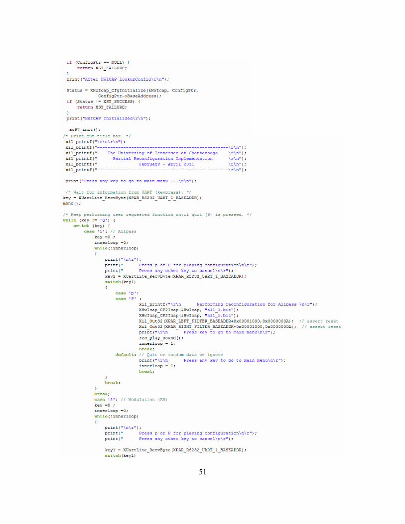
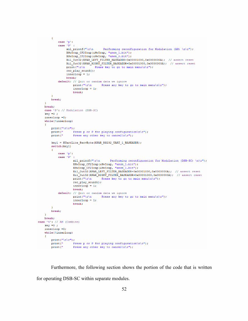
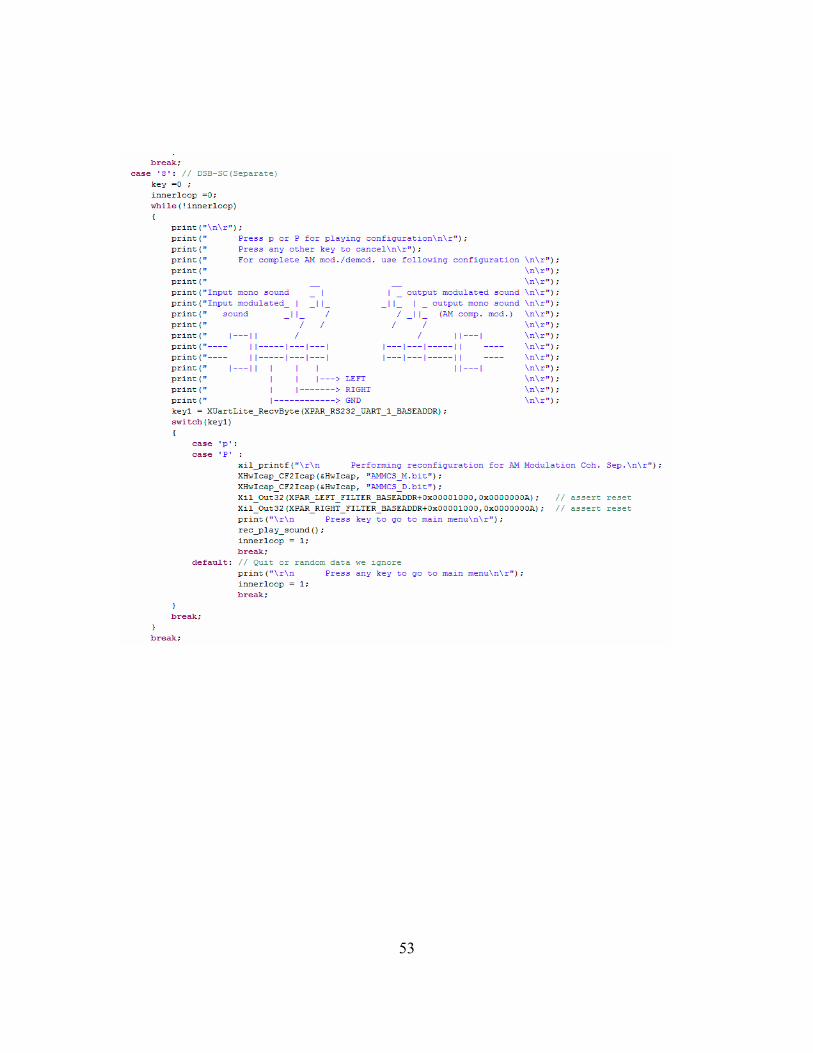
Xilinx tutorial. The software for this reconfigurable system was expanded from
approximately 750 lines of code to about 1,800 lines of code. The original portions of the
design are responsible for driving of audio chip on XUPV5 board and allowing the access
28
to Compact Flash memory card through Internal Configuration Access Port (ICAP) port.
ICAP allows writing software for an embedded processor (MicroBlaze) to modify the
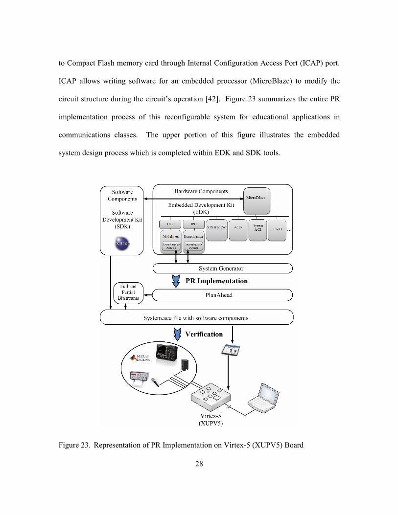
circuit structure during the circuit’s operation [42]. Figure 23 summarizes the entire PR
implementation process of this reconfigurable system for educational applications in
communications classes. The upper portion of this figure illustrates the embedded
system design process which is completed within EDK and SDK tools.
Figure 23. Representation of PR Implementation on Virtex-5 (XUPV5) Board
29
In addition, this figure shows that the netlist files for each reconfigurable partition
(RP) are generated by System Generator then the entire PR implantation process is
completed within PlanAhead. Also, after generating partial bitstreams and System ACE
file, they are transferred into a Compact Flash memory card for implementation on the
FPGA. System ACE stands for System Advanced Configuration Environment [43].
System ACE was developed by Xilinx to provide a cost saving alternative over
traditional PROMs by using Compact Flash memory cards [43]. The verification process
is done by observing that each partial bitstreams can swap on the FPGA without delaying
the operation of the board. In addition, a function generator is used for transmitting signal
through the system and observing the output signals through oscilloscope. In one part of
this process, the Simulink tool is used for modulating the signal and FPGA is used to act
as receiver by demodulating the signal. Next, the entire PR implementation process
describes in the following sections.
Partial Reconfiguration Implementation Process
The netlist files for each RP are generated within System Generator. In order to
create a PR design within PlanAhead it is required to have partial reconfiguration license
which was provided by Xilinx free of charge to universities for research and educational
applications. The following steps are required to generate partial bitstreams and System
ACE file for an FPGA [30]. This process is implemented for this reconfigurable system.
The users only need to follow some of these steps for their educational applications,
which are described in the next section.
30
(1) Setting-up PlanAhead
The first step is selecting PR option at the beginning of each PR project within
PlanAhead. Next the specific FPGA on the board is selected which is xc5vlx110tff1136-
1 for XUPV5 board.
(2) Selecting Top-level Netlist and Constraint file
In this step, the user should select the top netlist and constraint files of this design
that was generated by embedded design tool.
(3) Defining Reconfigurable Partitions
After selecting the top netlist, the next step is defining reconfigurable partitions
by right clicking on the instance and selecting Set Partition option.
(4) Adding Reconfigurable Modules
Next step is adding reconfigurable partitions for this design by right clicking on
the partition and selecting Add Reconfigurable Module. Next, the user should select
those netlist files that were generated by System Generator as the top level netlist for this
reconfigurable module.
(5) Defining RP Regions
In this step, the RP regions are defined. This process is part of a floorplanning
which refers to using AREA_GROUP constraints for controlling the design placement on
31
an FPGA [44]. Using AREA_GROUP constraints allows the user to keep all associated
logic with a partition concentrated in one area. This process will reduce the risk of
routing conflict, improve runtime, and improve timing results [44]. In PlanAhead the
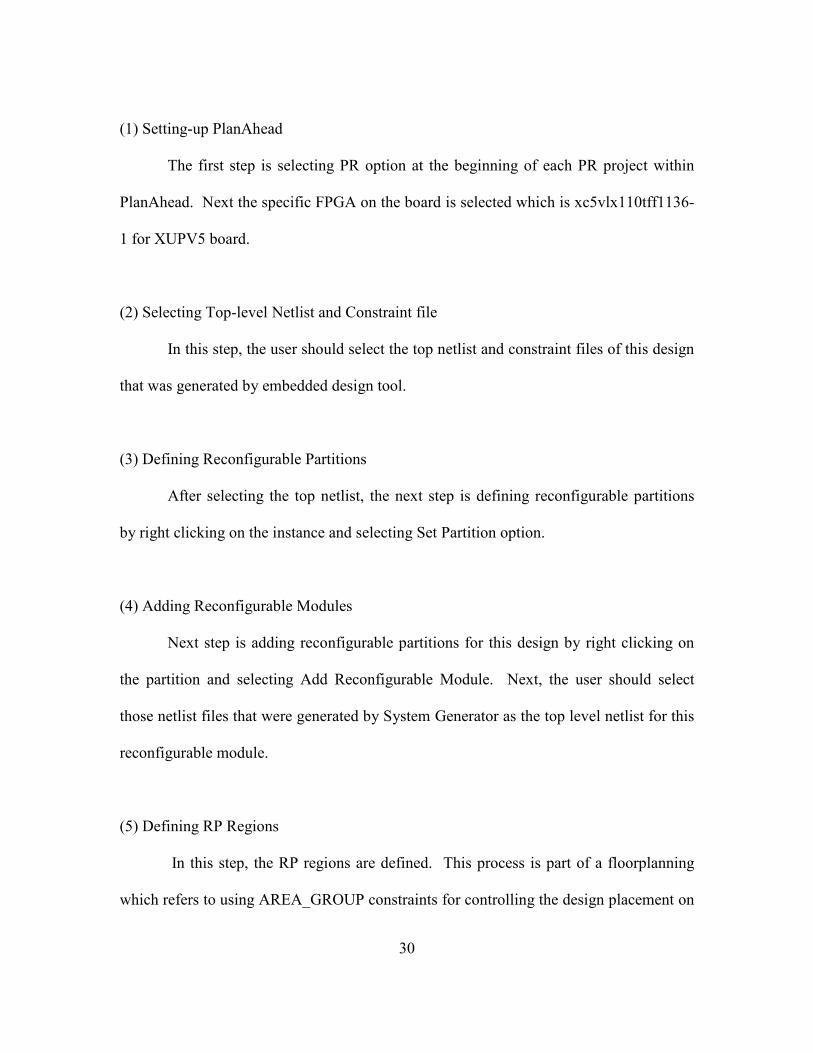
AREA_GROUP constraints are defined by a Pblock. Figure 24 shows the process of
defining the reconfigurable regions. In this figure, the Pblock size should be set under
the Physical Constraints pane. After right clicking in this pane and selecting Set Pblock
Size the user will be able to draw a rectangular shape for each RP.
In addition, PlanAhead will provide estimate of required resources for Pblock s of
each RP. The user should provide enough resources in this section by viewing physical
resource estimates for each partition in order complete the PR implementation
successfully. After saving the reconfigurable regions configuration will automatically
will save within the constraints file (system.ucf). These configurations can be edited and
updated within constraints file as well.
(6) Running Design Rule Checker
PlanAhead has option for catching the partial reconfiguration design issues at this
stage of implementation which is called Design Rule Checker (DRC).
(7) Creating Configuration
In this step, first implementation configuration is created by setting a new
synthesis strategy by using Xilinx Synthesis Technology (XST) tool. XST is part of ISE
Design Suite allowing synthesis of an HDL design. At this point the user can assign a
32
name to this configuration and select the appropriate partitions for it and then create it by
right clicking this configuration in Design Runs tab and selecting the Launch Runs. After
creating the first configuration (active configuration), this configuration should be
promoted to set the static logic of the design for entire PR implementation process.
Figure 24. Defining the Reconfigurable Regions
(8) Creating Additional Configurations
In this step, after promoting the first configuration, the additional configurations
can be generated by selecting Create Multiple Runs option under tools. In order to ensure
that the static regions and all other configurations interfaces all consistent, the user should
33
run the Verify Configuration option by right clicking on Configuration pane in
PlanAhead.
(9) Verifying PR Implementation
In this step, after verifying the configurations, the bitstreams can be generated by
right clicking on all of these configurations in Design Runs tab and selecting the Generate
Bitsteam option.
(10) Generating Bitstream Files and Image Files
In this step, the image file is created and implemented on the FPGA. This PR
design is using embedded soft (MicroBlaze) processor; therefore, the hardware bitstream
file must be merged with the software components. The main core of the software
components for this design is already created in the SDK. At this point, if there is need
for updating the software components that can be finalized by lunching SDK tool within
EDK and update the software components.
After updating the software components, these software components should
merge with the hardware bitstream. This process cannot be implemented within GUI of
PlanAhead and the user Xilinx bash shell will allow merging these components. The bash
shell can be access from EDK or SDK tools.
Finally, the partial bitstreams and system.ace files are copied on a compact flash
card for implantation on the XUPV5 board. In addition, if there is a need to add more
configurations later, they can be added at any time after completing the main PR project.
34
In order to add additional configurations, the user should only follow the following steps.
These steps are adding a new reconfigurable module, creating additional multiple runs,
selecting the Lunch Runs, and finally creating partial bitstreams for the new
configurations which makes this reconfigurable system a suitable system to use for
educational or research applications in communications classes.
Results of PR Implementation on the FPGA
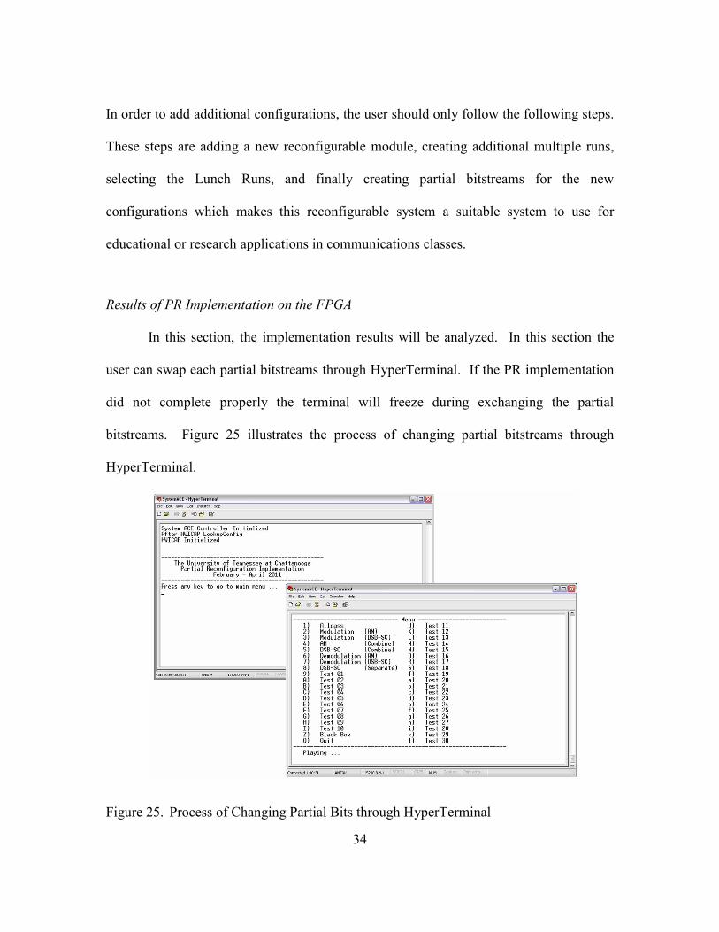
In this section, the implementation results will be analyzed. In this section the
user can swap each partial bitstreams through HyperTerminal. If the PR implementation
did not complete properly the terminal will freeze during exchanging the partial
bitstreams. Figure 25 illustrates the process of changing partial bitstreams through
HyperTerminal.
Figure 25. Process of Changing Partial Bits through HyperTerminal
35
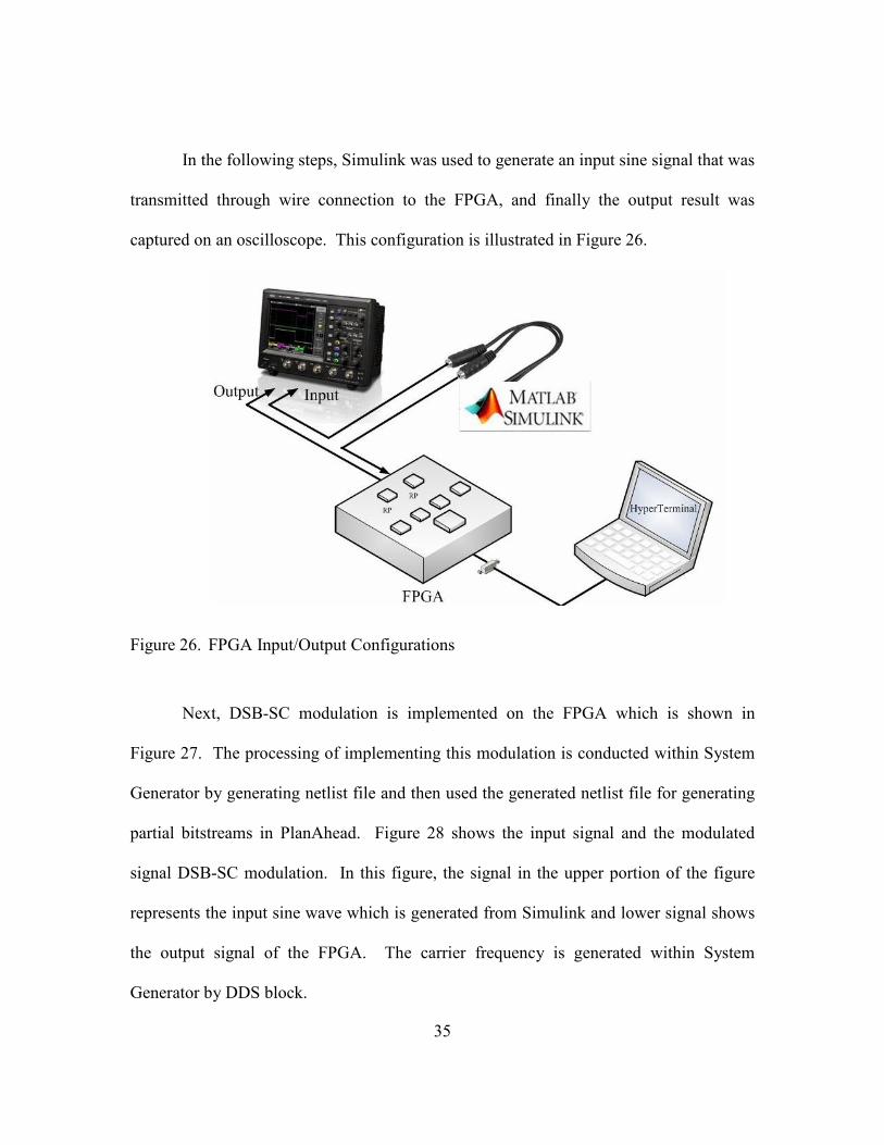
In the following steps, Simulink was used to generate an input sine signal that was
transmitted through wire connection to the FPGA, and finally the output result was
captured on an oscilloscope. This configuration is illustrated in Figure 26.
Figure 26. FPGA Input/Output Configurations
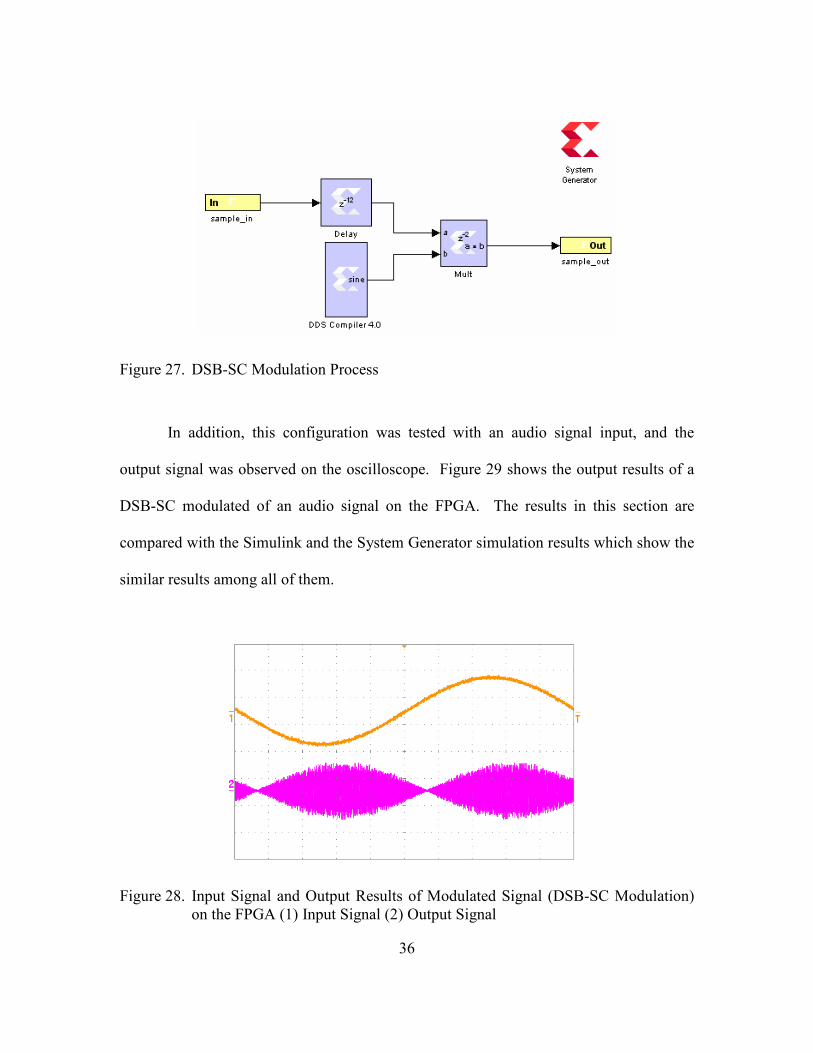
Next, DSB-SC modulation is implemented on the FPGA which is shown in
Figure 27. The processing of implementing this modulation is conducted within System
Generator by generating netlist file and then used the generated netlist file for generating
partial bitstreams in PlanAhead. Figure 28 shows the input signal and the modulated
signal DSB-SC modulation. In this figure, the signal in the upper portion of the figure
represents the input sine wave which is generated from Simulink and lower signal shows
the output signal of the FPGA. The carrier frequency is generated within System
Generator by DDS block.
36
Figure 27. DSB-SC Modulation Process
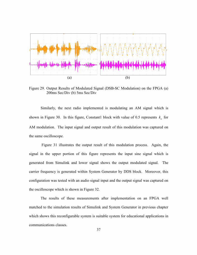
In addition, this configuration was tested with an audio signal input, and the
output signal was observed on the oscilloscope. Figure 29 shows the output results of a
DSB-SC modulated of an audio signal on the FPGA. The results in this section are
compared with the Simulink and the System Generator simulation results which show the
similar results among all of them.
Figure 28. Input Signal and Output Results of Modulated Signal (DSB-SC Modulation) on the FPGA (1) Input Signal (2) Output Signal
37
(a) (b)
Figure 29. Output Results of Modulated Signal (DSB-SC Modulation) on the FPGA (a) 200ms Sec/Div (b) 5ms Sec/Div
Similarly, the next radio implemented is modulating an AM signal which is
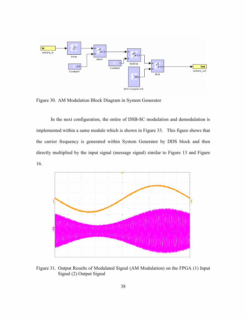
shown in Figure 30. In this figure, Constant1 block with value of 0.5 represents ak for
AM modulation. The input signal and output result of this modulation was captured on
the same oscilloscope.
Figure 31 illustrates the output result of this modulation process. Again, the
signal in the upper portion of this figure represents the input sine signal which is
generated from Simulink and lower signal shows the output modulated signal. The
carrier frequency is generated within System Generator by DDS block. Moreover, this
configuration was tested with an audio signal input and the output signal was captured on
the oscilloscope which is shown in Figure 32.
The results of these measurements after implementation on an FPGA well
matched to the simulation results of Simulink and System Generator in previous chapter
which shows this reconfigurable system is suitable system for educational applications in
communications classes.
38
Figure 30. AM Modulation Block Diagram in System Generator
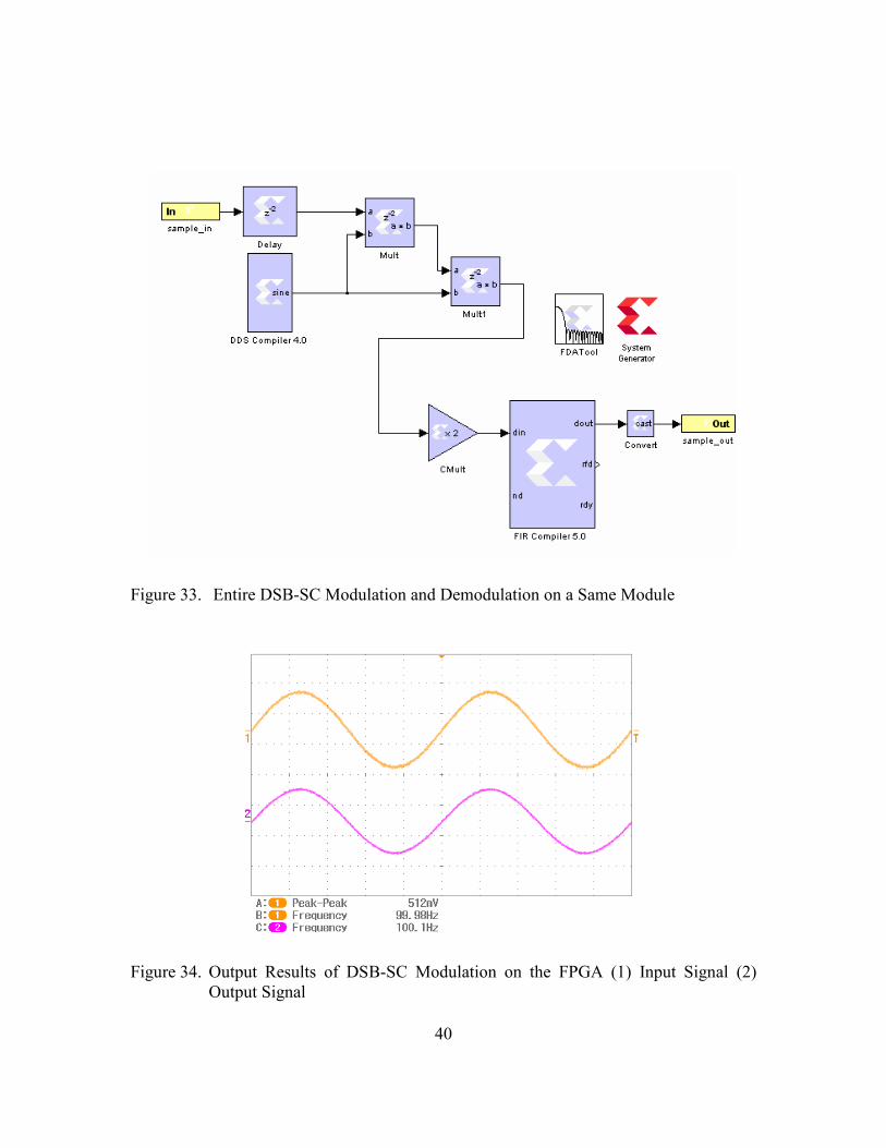
In the next configuration, the entire of DSB-SC modulation and demodulation is
implemented within a same module which is shown in Figure 33. This figure shows that
the carrier frequency is generated within System Generator by DDS block and then
directly multiplied by the input signal (message signal) similar to Figure 13 and Figure
16.
Figure 31. Output Results of Modulated Signal (AM Modulation) on the FPGA (1) Input Signal (2) Output Signal
39
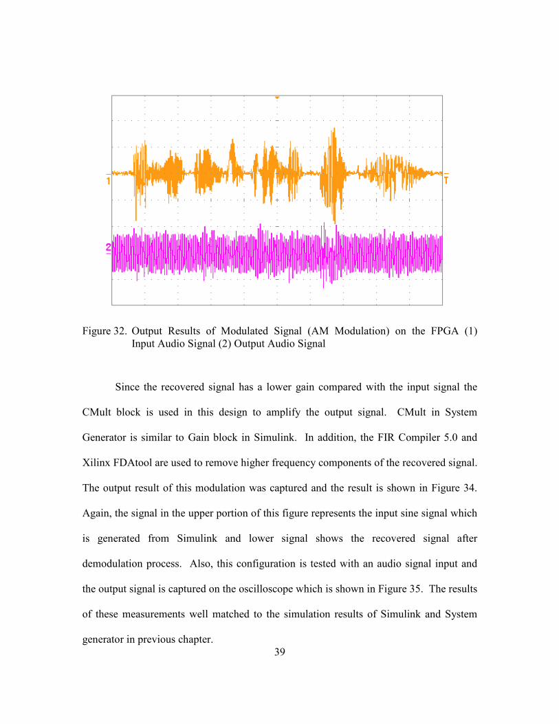
Figure 32. Output Results of Modulated Signal (AM Modulation) on the FPGA (1) Input Audio Signal (2) Output Audio Signal
Since the recovered signal has a lower gain compared with the input signal the
CMult block is used in this design to amplify the output signal. CMult in System
Generator is similar to Gain block in Simulink. In addition, the FIR Compiler 5.0 and
Xilinx FDAtool are used to remove higher frequency components of the recovered signal.
The output result of this modulation was captured and the result is shown in Figure 34.
Again, the signal in the upper portion of this figure represents the input sine signal which
is generated from Simulink and lower signal shows the recovered signal after
demodulation process. Also, this configuration is tested with an audio signal input and
the output signal is captured on the oscilloscope which is shown in Figure 35. The results
of these measurements well matched to the simulation results of Simulink and System
generator in previous chapter.
40
Figure 33. Entire DSB-SC Modulation and Demodulation on a Same Module
Figure 34. Output Results of DSB-SC Modulation on the FPGA (1) Input Signal (2) Output Signal
41
Figure 35. Output Results of DSB-SC Modulation on the FPGA (1) Input Audio Signal (2) Output Audio Signal
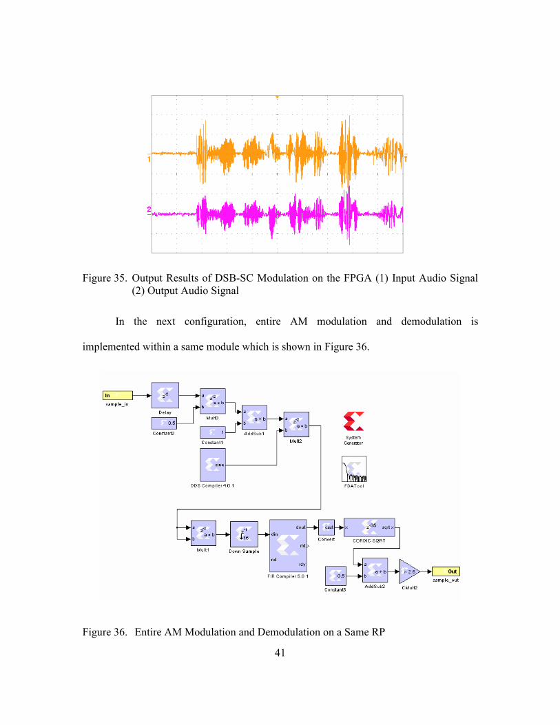
In the next configuration, entire AM modulation and demodulation is
implemented within a same module which is shown in Figure 36.
Figure 36. Entire AM Modulation and Demodulation on a Same RP
42
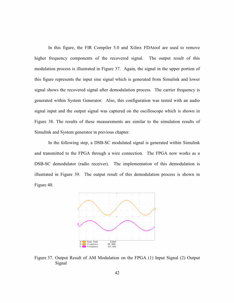
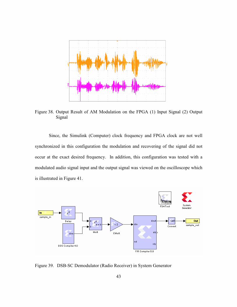
In this figure, the FIR Compiler 5.0 and Xilinx FDAtool are used to remove
higher frequency components of the recovered signal. The output result of this
modulation process is illustrated in Figure 37. Again, the signal in the upper portion of
this figure represents the input sine signal which is generated from Simulink and lower
signal shows the recovered signal after demodulation process. The carrier frequency is
generated within System Generator. Also, this configuration was tested with an audio
signal input and the output signal was captured on the oscilloscope which is shown in
Figure 38. The results of these measurements are similar to the simulation results of
Simulink and System generator in previous chapter.
In the following step, a DSB-SC modulated signal is generated within Simulink
and transmitted to the FPGA through a wire connection. The FPGA now works as a
DSB-SC demodulator (radio receiver). The implementation of this demodulation is
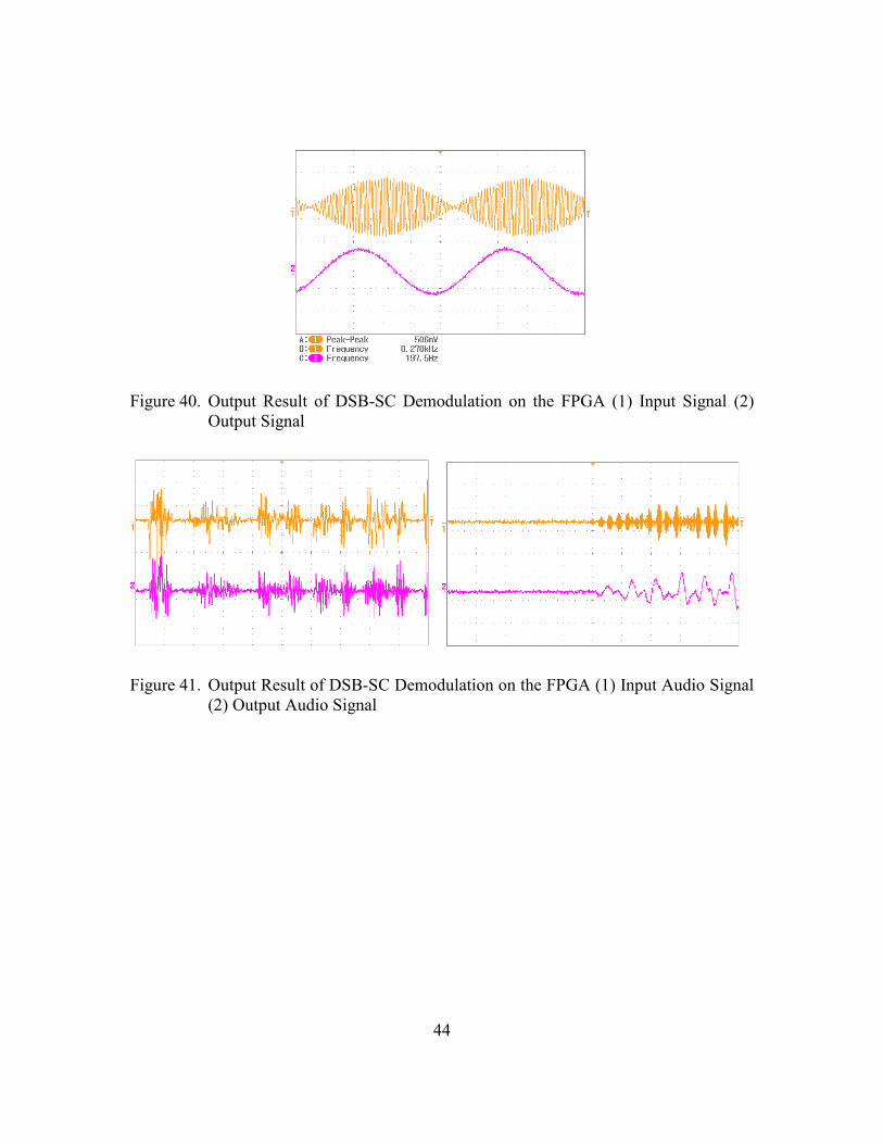
illustrated in Figure 39. The output result of this demodulation process is shown in
Figure 40.
Figure 37. Output Result of AM Modulation on the FPGA (1) Input Signal (2) Output Signal
43
Figure 38. Output Result of AM Modulation on the FPGA (1) Input Signal (2) Output Signal
Since, the Simulink (Computer) clock frequency and FPGA clock are not well
synchronized in this configuration the modulation and recovering of the signal did not
occur at the exact desired frequency. In addition, this configuration was tested with a
modulated audio signal input and the output signal was viewed on the oscilloscope which
is illustrated in Figure 41.
Figure 39. DSB-SC Demodulator (Radio Receiver) in System Generator
44
Figure 40. Output Result of DSB-SC Demodulation on the FPGA (1) Input Signal (2) Output Signal
Figure 41. Output Result of DSB-SC Demodulation on the FPGA (1) Input Audio Signal (2) Output Audio Signal
45
Chapter V
COCLUSIOS AD RECOMMEDATIOS
Conclusions
The objective of this thesis was to design, simulate, and implement partial
reconfigurable system for educational purposes on FPGAs. This objective was met by
investigating and modeling several designs within Simulink simulation tool. These
designs later were transferred and analyzed within System Generator, then implemented
within a PR design and finally implemented on a FPGA. After comparing the
simulations’ results of several modulation schemes on Simulink and System Generator to
the actual PR implementation on an FPGA, the results show that PR implementation was
done properly. Furthermore, the PR implementation shows that the additional
configurations can be design and implemented on an FPGA in few minutes rather than
few hours compared with the entire design implementation process. This capability will
make the PR implementation a useful tool for under graduate students in several of their
classes such as communications, digital signal processing, digital design, etc.
Future Recommendations
The current PR implementation does not take advantage of Tool Command
Language (Tcl). The PR implementation can be automated with use of Tcl commands
and reduce the time that is required to implement additional configurations. Also, due to
46
lack of additional XUPV5 Virtex board at the University of Tennessee at Chattanooga,
the performance of this partial reconfiguration was evaluated only on one XUPV5 Virtex
board. For the future work, these designs can be implemented and verified using several
FPGA boards. Another recommendation would be expanding these PR design in other
areas with SDR systems such as wireless network design.
47
REFERECES
[1] M. Lanzagorta, S. Bique, and R. Rosenberg, Introduction to Reconfigurable
Supercomputing. Morgan & Claypool Publishers, 2010.