86
EE 330 Lecture 36 Digital Circuit Design • Basic Logic Gates • Properties of Logic Families • Characterization of CMOS Inverter • One device sizing strategy • Multiple-input gates
EE 330
Lecture 36
Digital Circuit Design
• Basic Logic Gates
• Properties of Logic Families
• Characterization of CMOS Inverter
• One device sizing strategy
• Multiple-input gates

Exam 3 Friday April 13
Review session: Thursday 6pm

Rink includes effects of all loading
Must recalculate if any change in loading
Analysis systematic and rather simple
Formalization of cascade circuit analysis working
from load to input:
OUT 3 OUT 2
IN 1 2 3
1
IN
V V VV
V V V V
V
V
V1 Rin1
Vin
RS
Stage 1
Rin3
Stage 3Vout
RLRin2
Stage 2
V1 V3V2
Review from Last Lecture

High-gain amplifier
VIN
VOUT
Q1
VDD
VEE
IB
VIN
VOUT
Q1
mV
0
-gA
g
gmVBEVBE
iB
gπg0VIN
VOUT
8000AFV
t
V 200VA -
V 25mV
This gain is very large !
And no design parameters affect the gain
Review from Last Lecture

Current Sources/Mirrors
Q0
VCC
R
Q1
AE0 AE1
I1I0 I1
Current SinkKey Block
Biasing Circuit
Review from Last Lecture

Current Sources/Mirrors Summary
n-channel Current Mirror
M0 M1
W0,L0
Iout
Iin
W1,L1Q0
Q1
AE1
IOU T
I0
AE0
npn Current Mirror
01out in
0 1
LWI = I
W L
E1out in
E0
AI = I
A
Review from Last Lecture
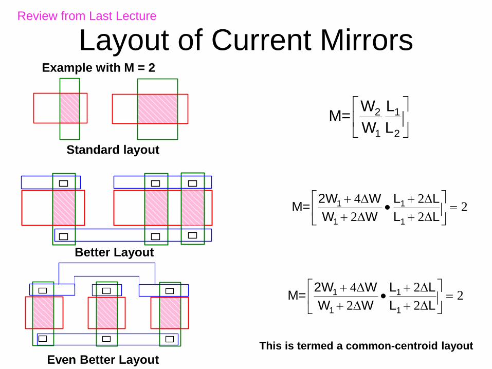
Layout of Current MirrorsExample with M = 2
2 1
1 2
W LM=
W L
Standard layout
Better Layout
4 22
2 21 1
1 1
2W W L LM=
W W L L
Even Better Layout
4 22
2 21 1
1 1
2W W L LM=
W W L L
This is termed a common-centroid layout
Review from Last Lecture
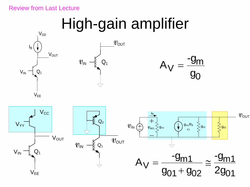
High-gain amplifier
VIN
VOUT
Q1
VDD
VEE
IB
VIN
VOUT
Q1 mV
0
-gA
g
VIN
VOUTQ1
Q2
VIN
VOUT
Q1
VEE
VCC
VYY gm1VB
E1VBE1
iB
gπ1g01 g02VIN
VOUT
m1 m1V
01 02 01
-g -gA
g g 2g
Review from Last Lecture
End of basic analog
Start of basic digital
Digital Circuit Design
• Hierarchical Design
• Basic Logic Gates
• Properties of Logic Families
• Characterization of CMOS
Inverter
• Static CMOS Logic Gates
– Ratio Logic
• Propagation Delay
– Simple analytical models
– Elmore Delay
• Sizing of Gates
• Propagation Delay with
Multiple Levels of Logic
• Optimal driving of Large
Capacitive Loads
• Power Dissipation in Logic
Circuits
• Other Logic Styles
• Array Logic
• Ring Oscillators
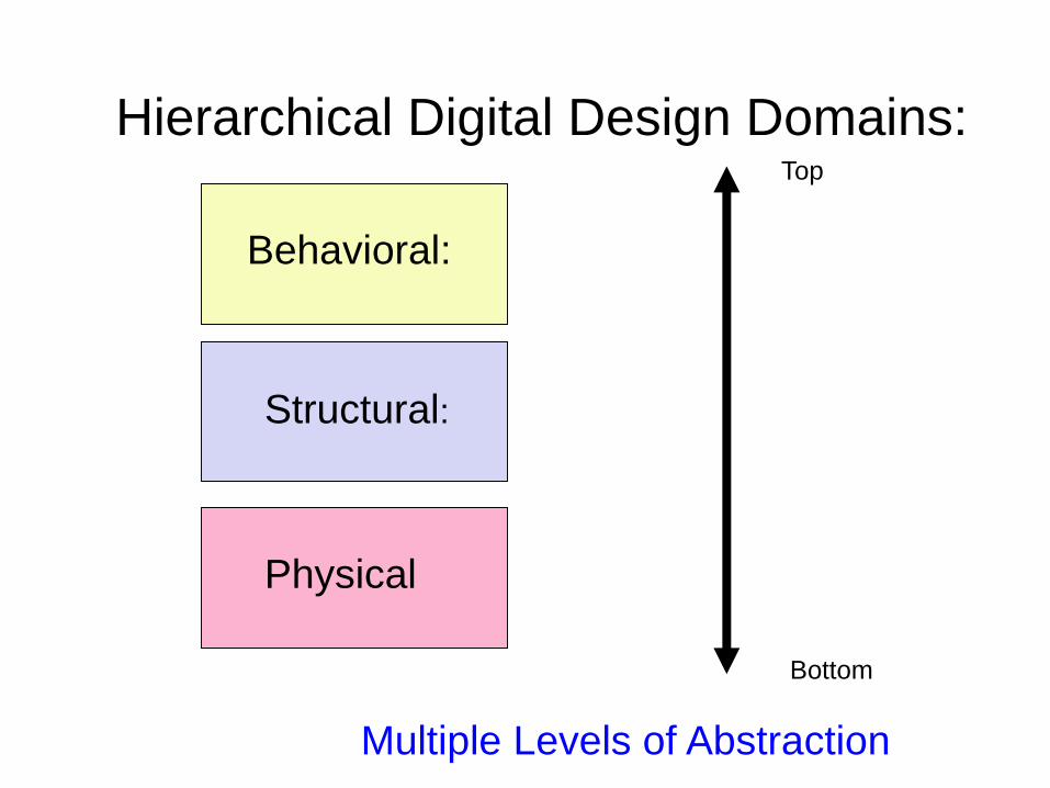
Hierarchical Digital Design Domains:
Behavioral:
Structural:
Top
Bottom
Physical
Multiple Levels of Abstraction

Hierarchical Digital Design Domains:
Behavioral:
Structural:
Top
Bottom
Physical Bott
om
Up D
esig
n
Top D
ow
n D
esig
n
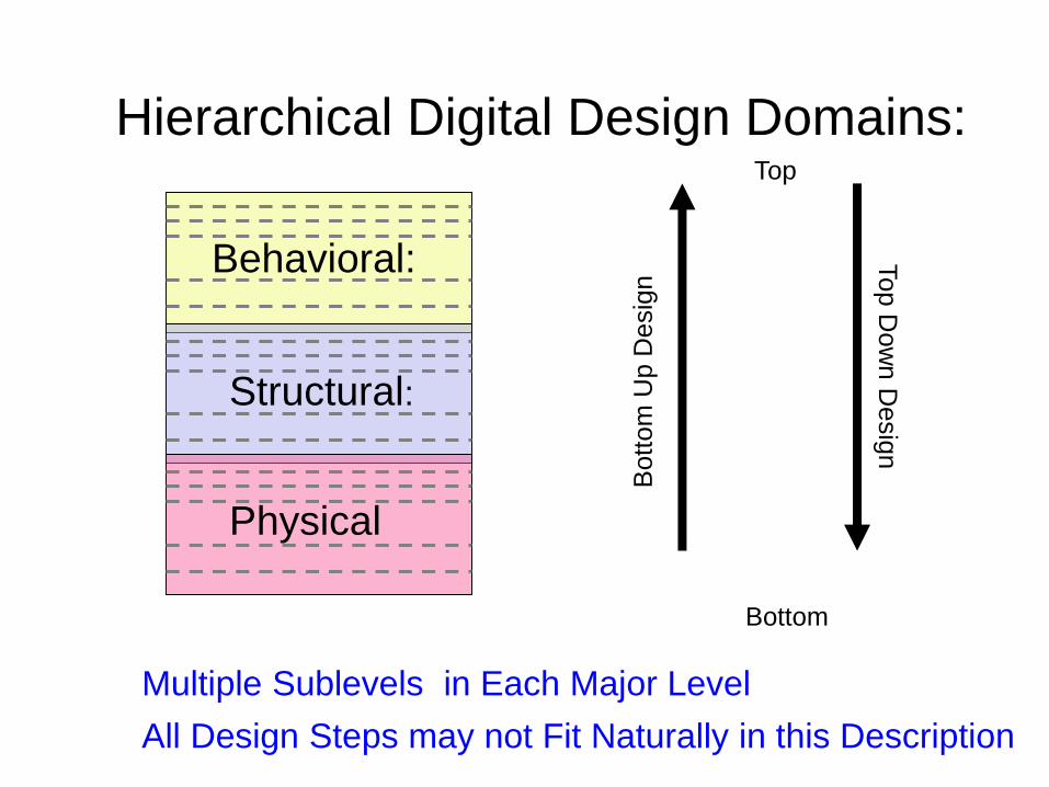
Hierarchical Digital Design Domains:Top
BottomB
ott
om
Up D
esig
n
Top D
ow
n D
esig
n
Behavioral:
Structural:
Physical
Multiple Sublevels in Each Major Level
All Design Steps may not Fit Naturally in this Description

Behavioral : Describes what a system does or what it should do
Structural : Identifies constituent blocks and describes how these
blocks are interconnected and how they interact
Physical : Describes the constituent blocks to both the
transistor and polygon level and their physical
placement and interconnection
Hierarchical Digital Design Domains:
Multiple representations often exist at any level or sublevel
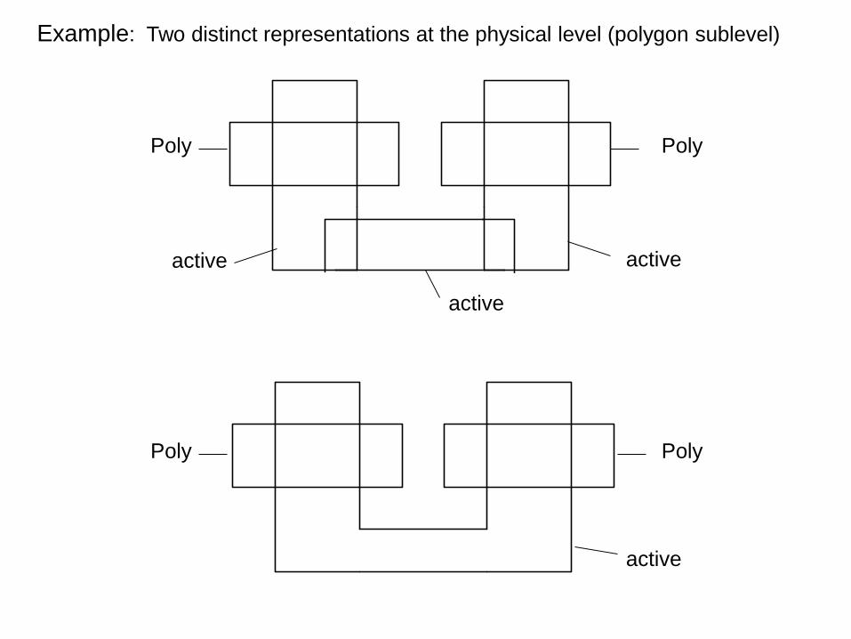
Example: Two distinct representations at the physical level (polygon sublevel)
Poly Poly
active
active
active
Poly Poly
active

Example: Two distinct representations at physical level (schematic sublevel)
W 4L
W 4
L 1
W 8
L 2
W1, LW2, L W1 + W2, L

Example: Two distinct representations at the structural/behavioral level (gate
sublevel)
A
B
C
A
B
C
cA
B
C A B
AB BA
In each domain, multiple levels of abstraction are generally used.
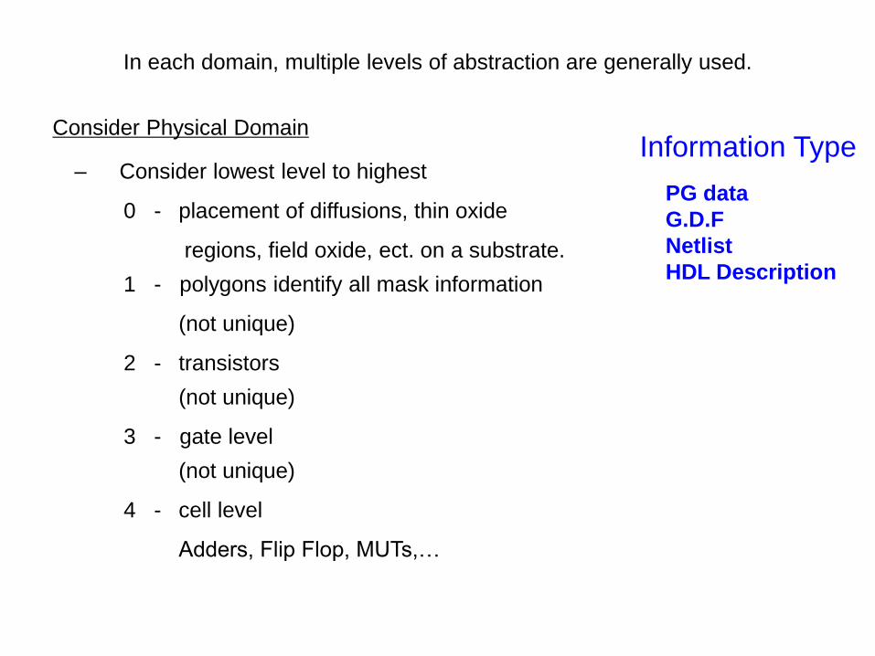
Consider Physical Domain
– Consider lowest level to highest
0 - placement of diffusions, thin oxide
regions, field oxide, ect. on a substrate.
1 - polygons identify all mask information
(not unique)
2 - transistors
(not unique)
3 - gate level
(not unique)
4 - cell level
Adders, Flip Flop, MUTs,…
PG data
G.D.F
Netlist
HDL Description
Information Type

Structural Level:
– DSP
– Blocks (Adders, Memory, Registers, etc.
– Gates
– Transistor
HDL
Netlists
Information Type
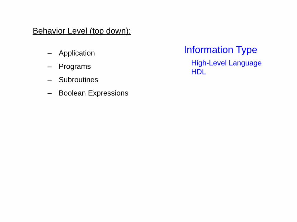
Behavior Level (top down):
– Application
– Programs
– Subroutines
– Boolean Expressions
High-Level Language
HDL
Information Type
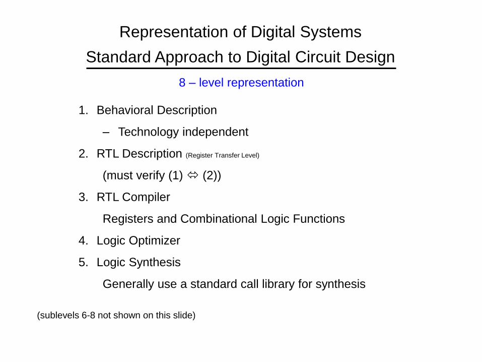
Representation of Digital Systems
Standard Approach to Digital Circuit Design
1. Behavioral Description
– Technology independent
2. RTL Description (Register Transfer Level)
(must verify (1) (2))
3. RTL Compiler
Registers and Combinational Logic Functions
4. Logic Optimizer
5. Logic Synthesis
Generally use a standard call library for synthesis
(sublevels 6-8 not shown on this slide)
8 – level representation
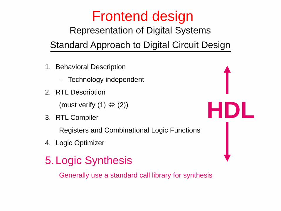
Representation of Digital Systems
Standard Approach to Digital Circuit Design
1. Behavioral Description
– Technology independent
2. RTL Description
(must verify (1) (2))
3. RTL Compiler
Registers and Combinational Logic Functions
4. Logic Optimizer
5.Logic Synthesis
Generally use a standard call library for synthesis
HDL
Frontend design

6.Place and Route
(physically locates all gates and registers and
interconnects them)
7. Layout Extraction
• DRC
• Back Annotation
8. Post Layout simulation
May necessitate a return to a higher level in the
design flow
Logic synthesis, though extensively used, often is not as efficient nor as
optimal for implementing some important blocks or some important
functions
These applications generally involve transistor level logic circuit design that
may combine one or more different logic design styles
Backend design
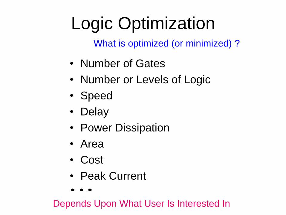
Logic Optimization
• Number of Gates
• Number or Levels of Logic
• Speed
• Delay
• Power Dissipation
• Area
• Cost
• Peak Current
What is optimized (or minimized) ?
Depends Upon What User Is Interested In
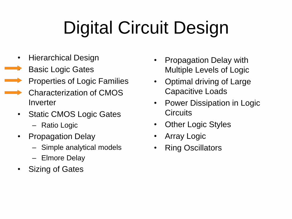
Digital Circuit Design
• Hierarchical Design
• Basic Logic Gates
• Properties of Logic Families
• Characterization of CMOS
Inverter
• Static CMOS Logic Gates
– Ratio Logic
• Propagation Delay
– Simple analytical models
– Elmore Delay
• Sizing of Gates
• Propagation Delay with
Multiple Levels of Logic
• Optimal driving of Large
Capacitive Loads
• Power Dissipation in Logic
Circuits
• Other Logic Styles
• Array Logic
• Ring Oscillators
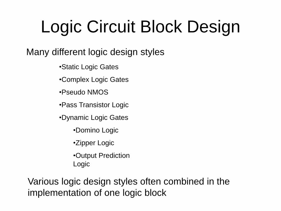
Logic Circuit Block Design
Many different logic design styles
•Static Logic Gates
•Complex Logic Gates
•Pseudo NMOS
•Pass Transistor Logic
•Dynamic Logic Gates
•Domino Logic
•Zipper Logic
•Output Prediction
Logic
Various logic design styles often combined in the
implementation of one logic block

The basic logic gates
X
X
Y
Y
Y
Y
Y
Y
Y
Y
A
A
A
A
A
A
B
B
B
B
B
B
XY
XY
BAY
BAY
BAY
BAY
BAY
BAY
AOIA
B
C
D
OAIA
B
C
D
Y
Y
A1
An
Y
A1
An
Y
A1
AnY
A1
AnY
DCBAY
DCBAY
n21 ...AAAY
n21 ...AAAY
n21 ...AAAY
n21 ...AAAY
Question: How many basic gates exist and how many of these are useful?

The set of NOR gates is complete
Any combinational logic function can be realized with only multiple-input NOR gates
The set of NAND gates is completeAny combinational logic function can be realized with
only multiple-input NOR gates
Performance of the BASIC gates is critical!
The basic logic gates

The basic logic gates
It suffices to characterize the inverter of a logic
family and then express the performance of
other gates in that family in terms of the
performance of the inverter.
What characteristics are required and desirable for an inverter to form the
basis for a useful logic family?

Desirable and/or Required Logic
Family Characteristics
1. High and low logic levels must be uniquely
distinguishable (even in a long cascade)
2. Capable of driving many loads (good fanout)
3. Fast transition times (but in some cases, not
too fast)
4. Good noise margins (low error probabilities)
5. Small die area
6. Low power consumption
7. Economical process requirements
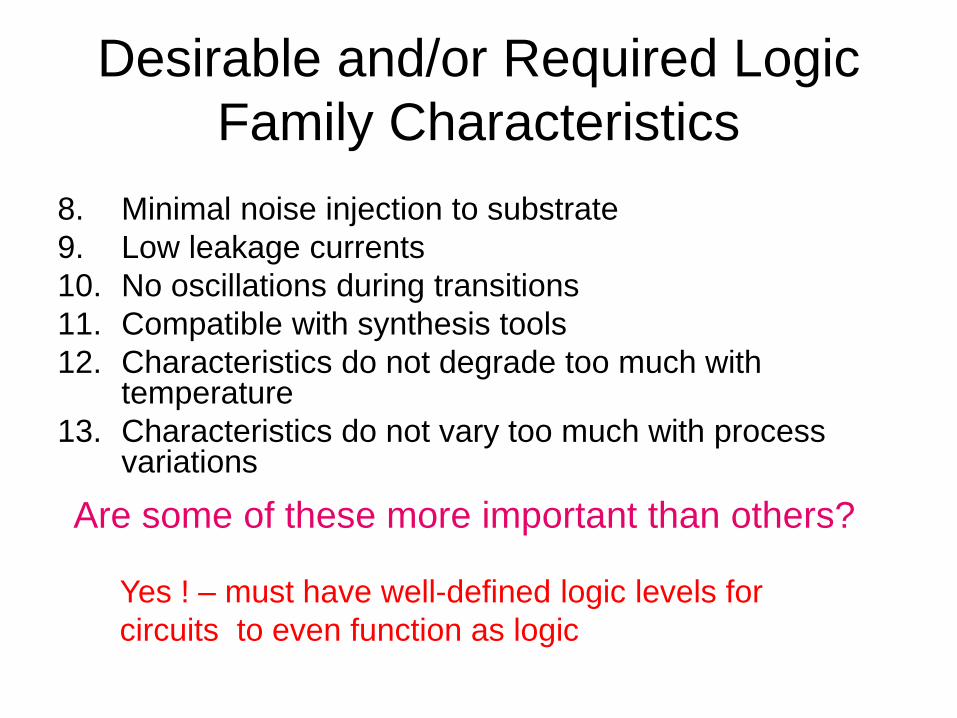
Desirable and/or Required Logic
Family Characteristics
8. Minimal noise injection to substrate
9. Low leakage currents
10. No oscillations during transitions
11. Compatible with synthesis tools
12. Characteristics do not degrade too much with temperature
13. Characteristics do not vary too much with process variations
Are some of these more important than others?
Yes ! – must have well-defined logic levels for
circuits to even function as logic

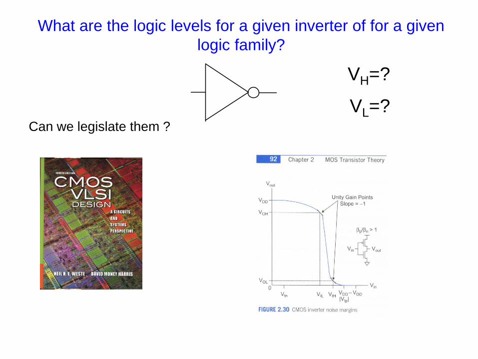
What are the logic levels for a given inverter of for a given
logic family?
VH=? VL=?
Can we legislate them ?• Some authors choose to simply define a value for them
• Simple and straightforward approach
• But what if the circuit does not interpret them the same way
they are defined !!

What are the logic levels for a given inverter of for a given
logic family?
VH=?
VL=?Can we legislate them ?
World’s most widely used electronics text
What are the logic levels for a given inverter of for a given
logic family?
VH=?
VL=?Can we legislate them ?

What are the logic levels for a given inverter of for a given
logic family?
VH=? VL=?
Can we legislate them ?• Some authors choose to define them based upon specific features of inverter
• Analytical expressions may be complicated
• But what if the circuit does not interpret them the same way they are defined !!
VOUT
VIN
VL VH
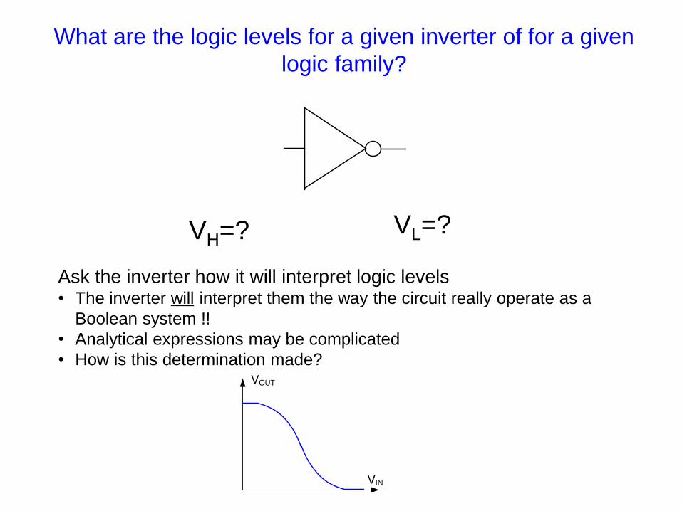
What are the logic levels for a given inverter of for a given
logic family?
VH=? VL=?
Ask the inverter how it will interpret logic levels• The inverter will interpret them the way the circuit really operate as a
Boolean system !!
• Analytical expressions may be complicated
• How is this determination made?VOUT
VIN
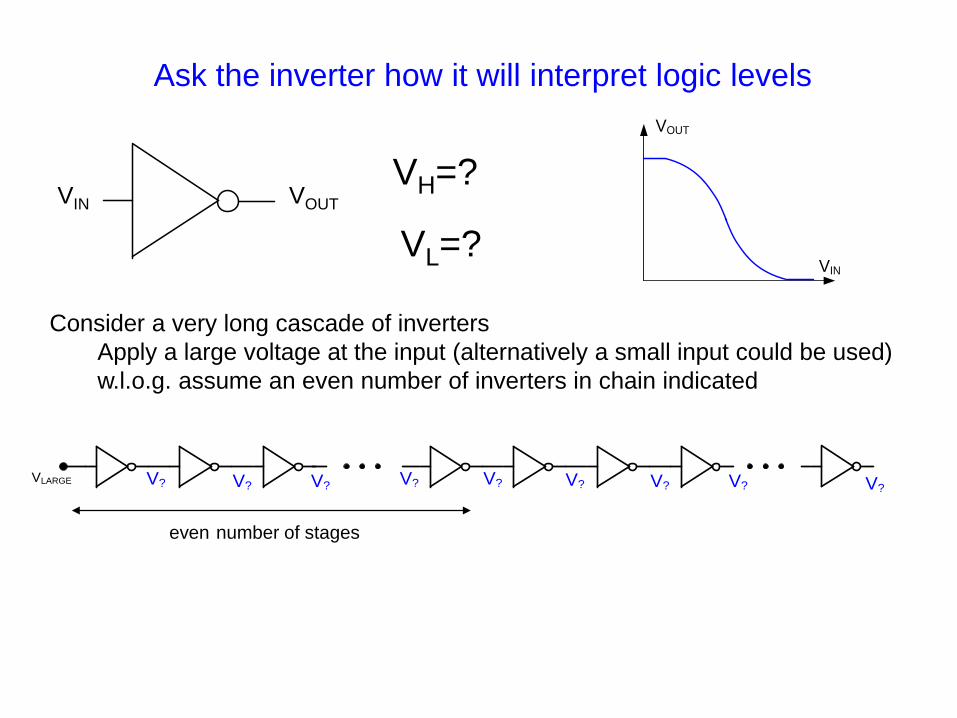
Ask the inverter how it will interpret logic levels
VH=?
VL=?
VOUT
VIN
VIN VOUT
VLARGE V? V?V? V?V?V? V? V? V?
Consider a very long cascade of inverters
Apply a large voltage at the input (alternatively a small input could be used)
w.l.o.g. assume an even number of inverters in chain indicated
even number of stages

Ask the inverter how it will interpret logic levels
VH=?
VL=?
VOUT
VIN
VIN VOUT
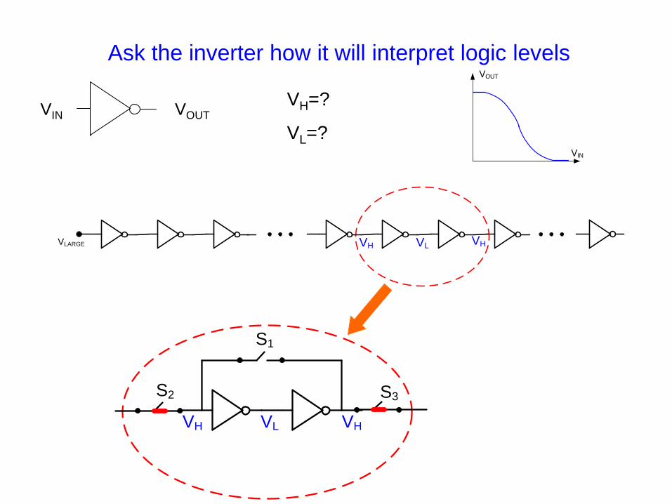
VLARGE VH VHVL VLVLV? V? V? VL VHor
Consider a very long cascade of inverters
Apply a large voltage at the input (alternatively a small input could be used)
w.l.o.g. assume an even number of inverters in chain indicated
even number of stages
If logic levels are to be maintained, the voltage at the end of this even
number of stages must be VH, that of the next must be VL, the next VH, etc.
until the start of the cascade is approached
Ask the inverter how it will interpret logic levels
VH=?
VL=?
VOUT
VIN
VIN VOUT
VLARGE VH VHVL
S1
S2 S3
VH VHVL
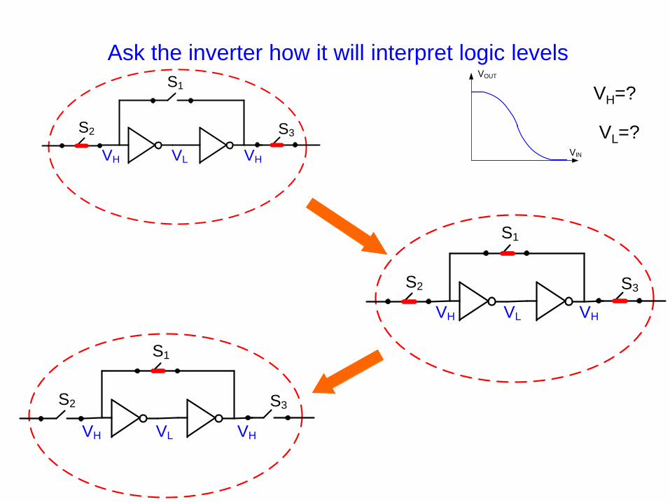
Ask the inverter how it will interpret logic levels
VH=?
VL=?
VOUT
VIN
S1
S2 S3
VH VHVL
S1
S2 S3
VH VHVL
S1
S2 S3
VH VHVL

Ask the inverter how it will interpret logic levels
VH=?
VL=?
VOUT
VIN
S1
S2 S3
VH VHVL
• Two inverter loop
• Very useful circuit !
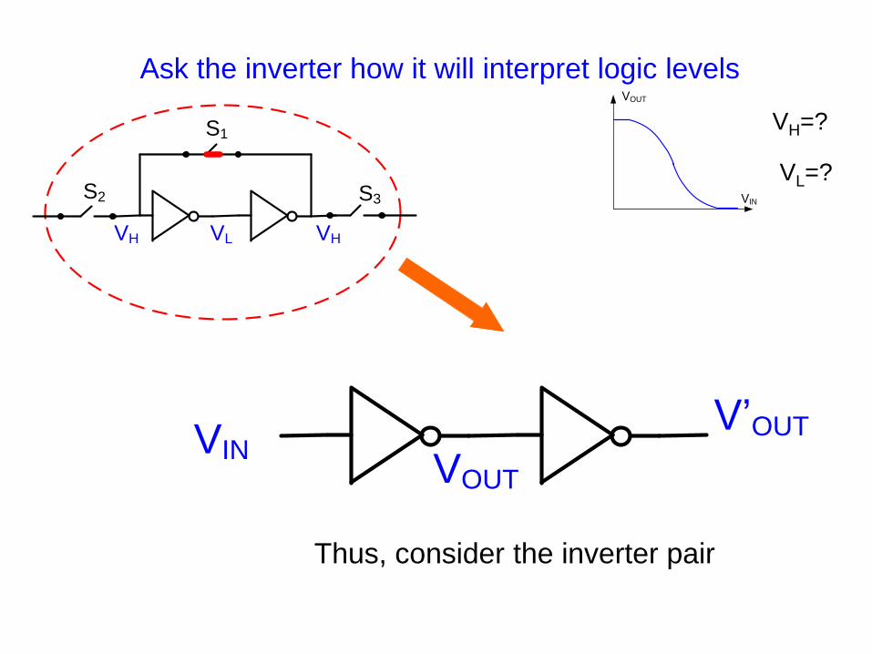
Ask the inverter how it will interpret logic levels
VH=?
VL=?
VOUT
VIN
S1
S2 S3
VH VHVL
VINVOUT
V’OUT
Thus, consider the inverter pair

Ask the inverter how it will interpret logic levels
VH=?
VL=?
VOUT
VIN
VINVOUT
V’OUT
Inverter pair
V’OUT
VIN
VH and VL will be on the intersection of the transfer
characteristics of the inverter pair (IPTC) and the V’OUT=VIN
line
V’OUT=VIN
VH and VL often termed the “1” and “0” states

Ask the inverter how it will interpret logic levels
VINVOUT
V’OUT
Inverter pair
V’OUT
VIN
VL VHVTRIP
When V’OUT=VIN, VH and VL are stable operating points, VTRIP is a
quasi-stable operating point
Observe: slope of IPTC is greater than 1 at VTRIP and less than 1 at VH and VL

Observation
VINVOUT
V’OUT
V’OUT
VIN
VL VHVTRIP
1
1
When VOUT=VIN for the inverter, V’OUT is also equal to VIN . Thus the intersection
point for VOUT=VIN in the inverter transfer characteristics (ITC) is also an intersection
point for V’OUT=VIN in the inverter-pair transfer characteristics (IPTC)
VOUT
VIN
VTRIP
1
1
Implication: Inverter characteristics can be used directly to obtain VTRIP

Logic Family Characteristics
What are the logic levels for a given inverter of for a given logic family?
What properties of an inverter are necessary for it to be useful for building a
two-level logic family?
The inverter-pair transfer characteristics must have three unique
intersection points with the V’OUT = VIN line
The two extreme intersection points of the inverter-pair transfer
characteristics with the V’OUT = VIN line
Can we legislate VH and VL for a logic family ?
What other properties of the inverter are desirable?
Reasonable separation between VH and VL (enough separation so that
noise does not cause circuit to interpret level incorrectly)
H L
TRIP
V +VV
2 (to provide adequate noise immunity and process insensitivity)
No!
V’OUT
VIN
VL VHVTRIP
1
1

What happens near the quasi-stable
operating point?
S2
S1 S1
S2
S1 S1
S1
X Y
S2 closed and X=Y=VTRIP
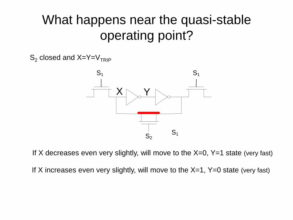
What happens near the quasi-stable
operating point?
S2
S1 S1
S1
X Y
S2 closed and X=Y=VTRIP
If X decreases even very slightly, will move to the X=0, Y=1 state (very fast)
If X increases even very slightly, will move to the X=1, Y=0 state (very fast)
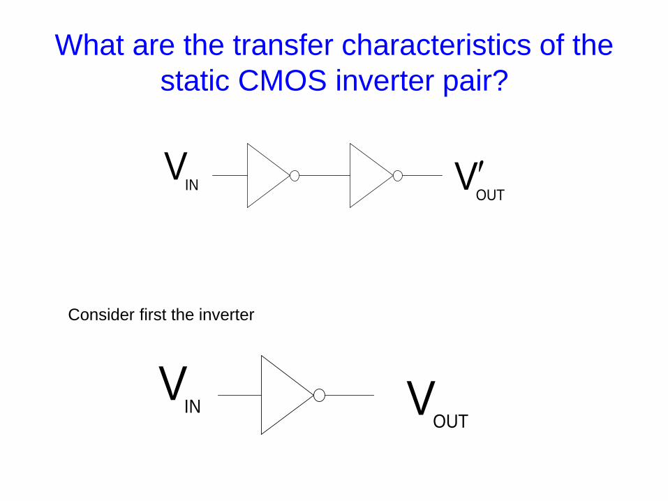
What are the transfer characteristics of the
static CMOS inverter pair?
INV
OUTV
INV
OUTV
Consider first the inverter
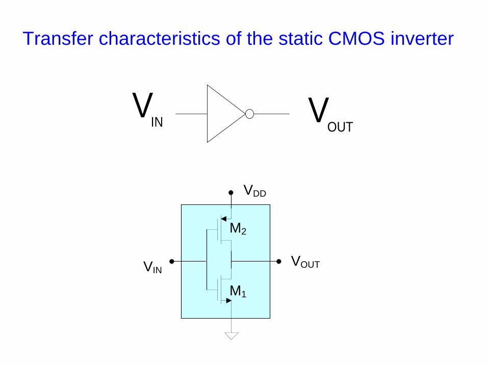
Transfer characteristics of the static CMOS inverter
INV
OUTV
M1
M2
VDD
VINVOUT
Transfer characteristics of the static CMOS inverter
M1
M2
VDD
VINVOUT
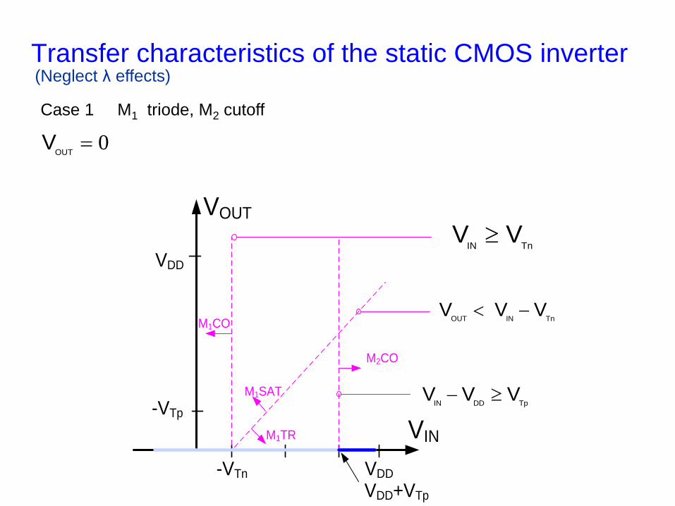
Case 1 Vin is so high that M1 triode, M2 cutoff
OUT1
D1 n OXn IN Tn OUT
1
VWI μ C V V V
L 2
GS1 Tn DS1 GS1 TnV V V V V
0D2I
0 OUT1
n OXn IN Tn OUT
1
VWμ C V V V
L 2
0OUT
V
GS2 TpV V
Equating ID1 and –ID2 we
obtain:
It can be shown that setting the first product term to 0 will not verify, thus
valid for:
IN Tn OUT IN TnV V V V V
IN DD TpV V V
thus, valid for:
(Neglect λ effects)
IN Tn OUT IN TnV V V V V
IN DD TpV V V
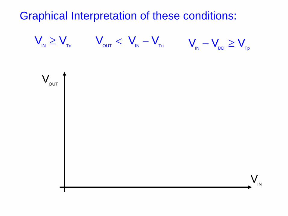
Graphical Interpretation of these conditions:
OUTV
INV
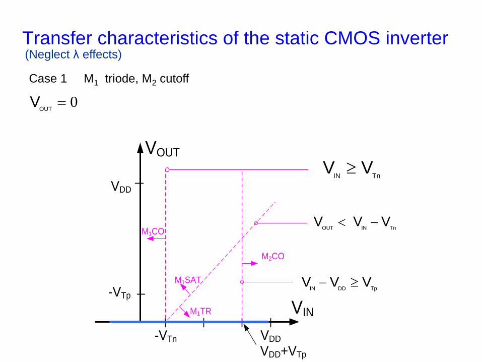
Transfer characteristics of the static CMOS inverter
Case 1 M1 triode, M2 cutoff
0OUT
V
OUT IN TnV V V
IN DD TpV V V
IN TnV V
VDD
VDD
VIN
VOUT
-VTp
-VTn
VDD+VTp
M2CO
M1CO
M1TR
M1SAT
(Neglect λ effects)
Transfer characteristics of the static CMOS inverter
Case 1 M1 triode, M2 cutoff
0OUT
V
OUT IN TnV V V
IN DD TpV V V
IN TnV V
VDD
VDD
VIN
VOUT
-VTp
-VTn
VDD+VTp
M2CO
M1CO
M1TR
M1SAT
(Neglect λ effects)
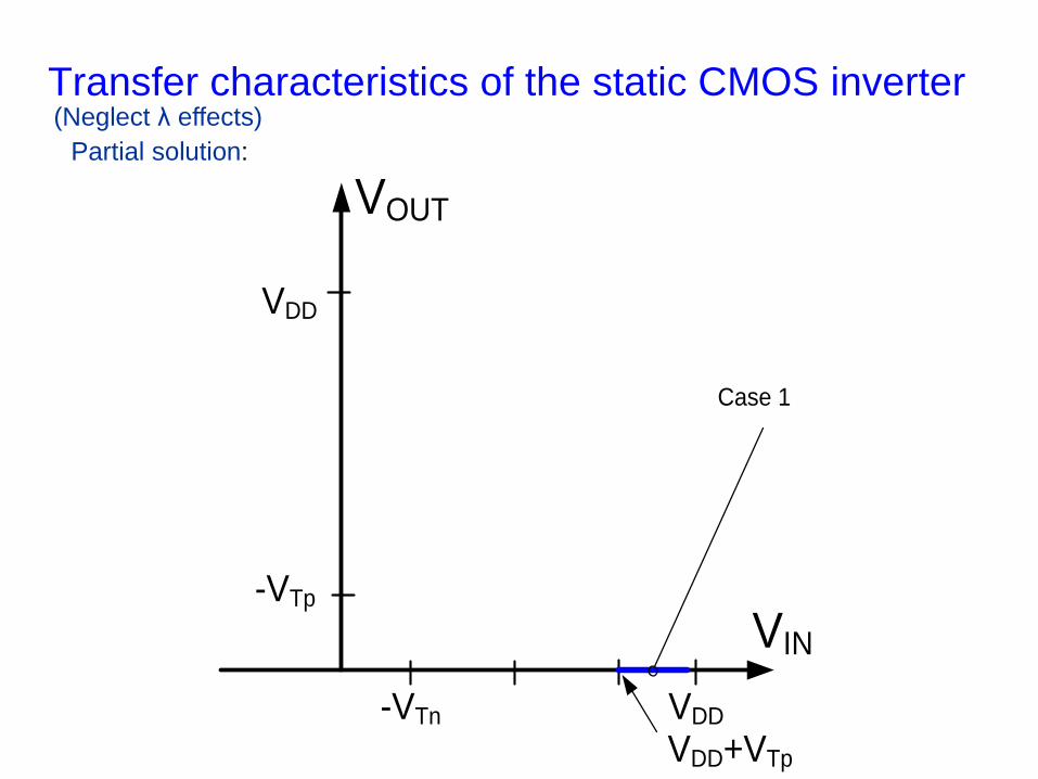
Transfer characteristics of the static CMOS inverter
VDD
VDD
VIN
VOUT
-VTp
-VTn
VDD+VTp
Case 1
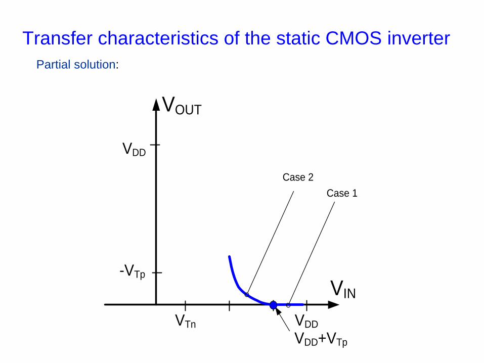
Partial solution:
(Neglect λ effects)
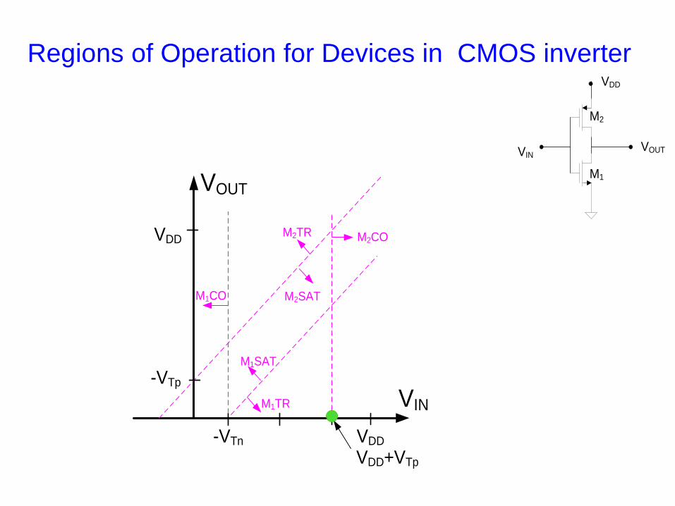
Regions of Operation for Devices in CMOS inverter
VDD
VDD
VIN
VOUT
-VTp
-VTn
VDD+VTp
M2CO
M1CO
M1TR
M2TR
M2SAT
M1SAT
M1
M2
VDD
VINVOUT

Transfer characteristics of the static CMOS inverter
Case 2 M1 triode, M2 sat
VDD
VDD
VIN
VOUT
-VTp
VTn
VDD+VTp
M2CO
M1CO
M1TR
M2TR
M2SAT
M1SAT
(Neglect λ effects)
M2: Square law ID
M1: like a resistor
: square law Vout

Transfer characteristics of the static CMOS inverter
M1
M2
VDD
VINVOUT
Case 2 M1 triode, M2 sat
OUT1
D1 n OXn IN Tn OUT
1
VWI μ C V V V
L 2
GS1 Tn DS1 GS1 TnV V V V V GS2 Tp DS2 GS2 T2
V V V V -V
Equating ID1 and –ID2 we obtain:
valid for:
IN Tn OUT IN TnV V V V V
IN DD Tp OUT DD IN DD TpV V V V -V V -V -V
thus, valid for:
2
p OXp 2
D2 IN DD Tp
2
μ C WI V V V
2 L
2
p OXp OUT2 1
IN DD Tp n OXn IN Tn OUT
2 1
μ C VW WV V V μ C V V V
2 L L 2
(Neglect λ effects)
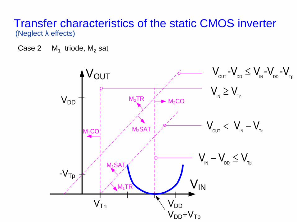
Transfer characteristics of the static CMOS inverter
Case 2 M1 triode, M2 sat
VDD
VDD
VIN
VOUT
-VTp
VTn
VDD+VTp
M2CO
M1CO
M1TR
M2TR
M2SAT
M1SAT
IN TnV V
OUT IN TnV V V
IN DD TpV V V
OUT DD IN DD TpV -V V -V -V
(Neglect λ effects)

Transfer characteristics of the static CMOS inverter
Case 2 M1 triode, M2 sat
VDD
VDD
VIN
VOUT
-VTp
VTn
VDD+VTp
M2CO
M1CO
M1TR
M2TR
M2SAT
M1SAT
IN TnV V
OUT IN TnV V V
IN DD TpV V V
OUT DD IN DD TpV -V V -V -V
(Neglect λ effects)
Transfer characteristics of the static CMOS inverter
VDD
VDD
VIN
VOUT
-VTp
VTn
VDD+VTp
Case 1
Case 2
Partial solution:
Transfer characteristics of the static CMOS inverter
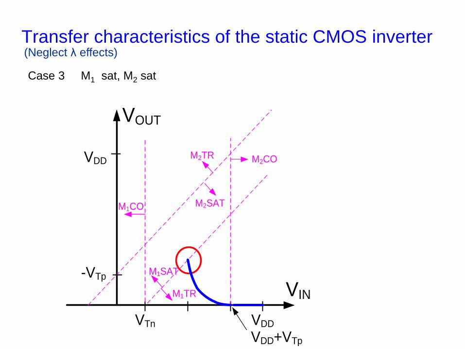
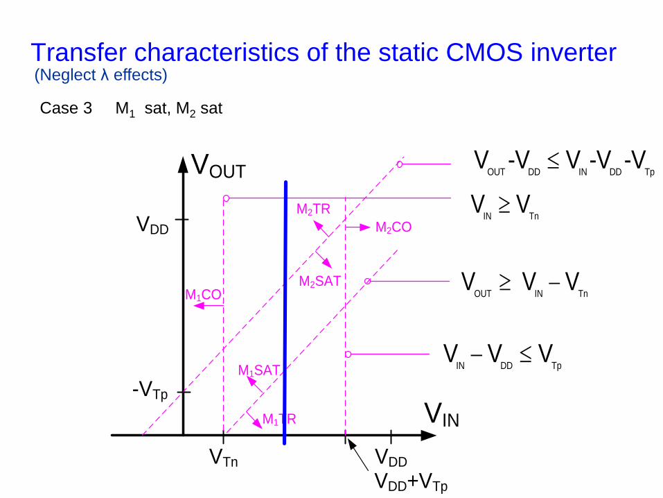
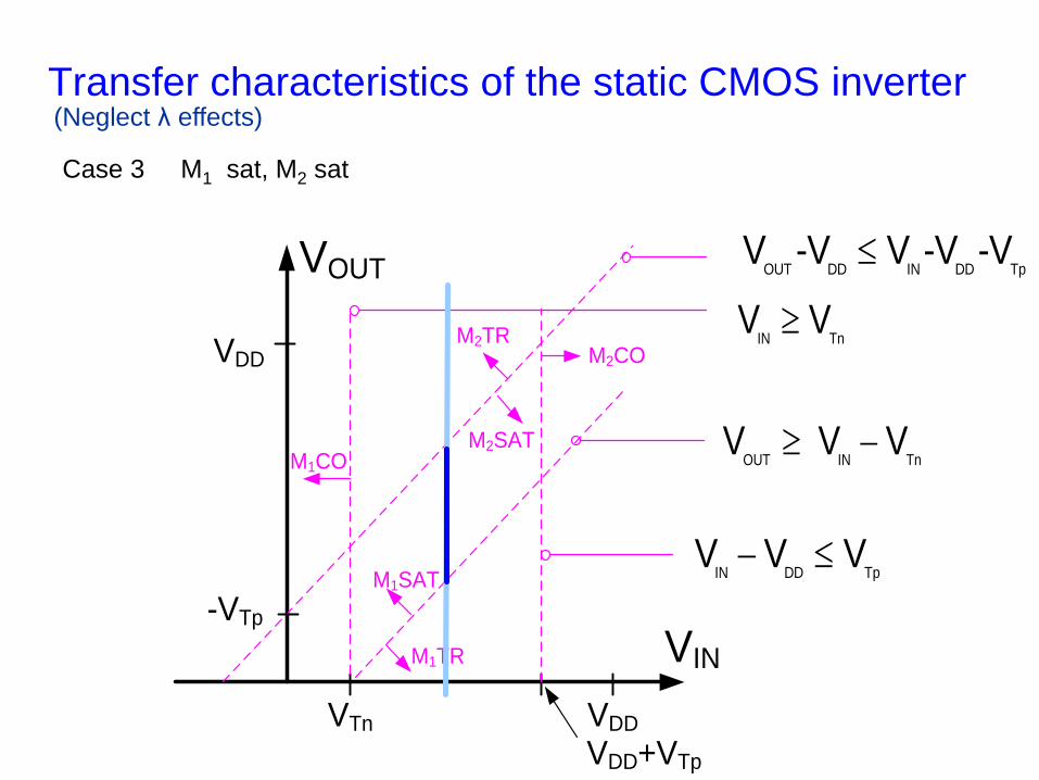
Case 3 M1 sat, M2 sat
VDD
VDD
VIN
VOUT
-VTp
VTn
VDD+VTp
M2CO
M1CO
M1TR
M2TR
M2SAT
M1SAT
(Neglect λ effects)
Transfer characteristics of the static CMOS inverter
M1
M2
VDD
VINVOUT
Case 3 M1 sat, M2 sat
2
2n OXn 1
D1 IN Tn
1
μ C WI V V
L
Equating ID1 and –ID2 we obtain:
2
p OXp 2
D2 IN DD Tp
2
μ C WI V V V
2 L
2 2
p OXp n OXn2 1
IN DD Tp IN Tn
2 1
μ C μ CW WV V V V V
2 L 2 L
p OXp n OXn2 1
DD Tp IN IN Tn
2 1
μ C μCW WV +V V V V
2 L 2 L
p OXpn OXn 1 2
Tn DD Tp
1 2
IN
p OXpn OXn 1 2
1 2
μ Cμ C W WV V +V
2 L 2 LV
μ Cμ C W W
2 L 2 L
Which can be rewritten as:
Which can be simplified to:
This is a vertical line
(Neglect λ effects)
Transfer characteristics of the static CMOS inverter
M1
M2
VDD
VINVOUT
Case 3 M1 sat, M2 sat
p OXpn OXn 1 2
Tn DD Tp
1 2
IN
p OXpn OXn 1 2
1 2
μ Cμ C W WV V +V
2 L 2 LV
μ Cμ C W W
2 L 2 L
Since this can be simplified to:OXn OXp OX
C C =C
p1 2
Tn DD Tp
1 n 2
IN
p1 2
1 n 2
μW WV V +V
L μ LV
μW W
L μ L
GS1 Tn DS1 GS1 TnV V V V V
valid for:
GS2 Tp DS2 GS2 T2V V V V -V
thus, valid for:
IN Tn OUT IN TnV V V V V IN DD Tp OUT DD IN DD Tp
V V V V -V V -V -V
(Neglect λ effects)
Transfer characteristics of the static CMOS inverter
Case 3 M1 sat, M2 sat
VDD
VDD
VIN
VOUT
-VTp
VTn
VDD+VTp
M2CO
M1CO
M1TR
M2TR
M2SAT
M1SAT
IN TnV V
OUT IN TnV V V
IN DD TpV V V
OUT DD IN DD TpV -V V -V -V
(Neglect λ effects)
Transfer characteristics of the static CMOS inverter
Case 3 M1 sat, M2 sat
VDD
VDD
VIN
VOUT
-VTp
VTn
VDD+VTp
M2CO
M1CO
M1TR
M2TR
M2SAT
M1SAT
IN TnV V
OUT IN TnV V V
IN DD TpV V V
OUT DD IN DD TpV -V V -V -V
(Neglect λ effects)
Transfer characteristics of the static CMOS inverter
VDD
VDD
VIN
VOUT
-VTp
VTn
VDD+VTp
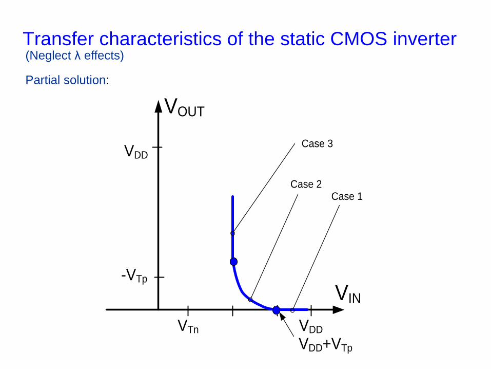
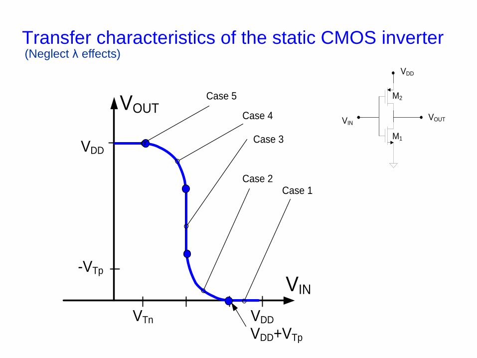
Case 1Case 2
Case 3
Partial solution:
(Neglect λ effects)
Transfer characteristics of the static CMOS inverter
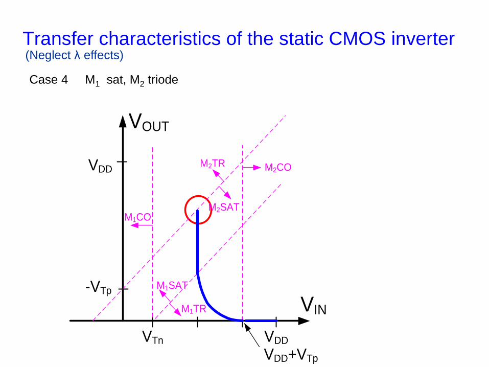
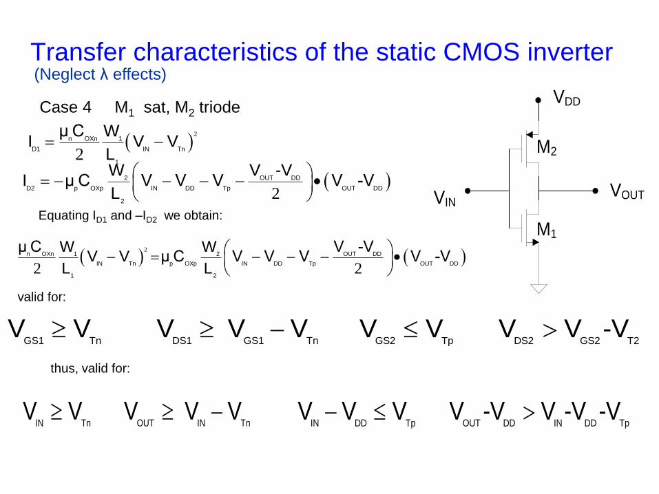
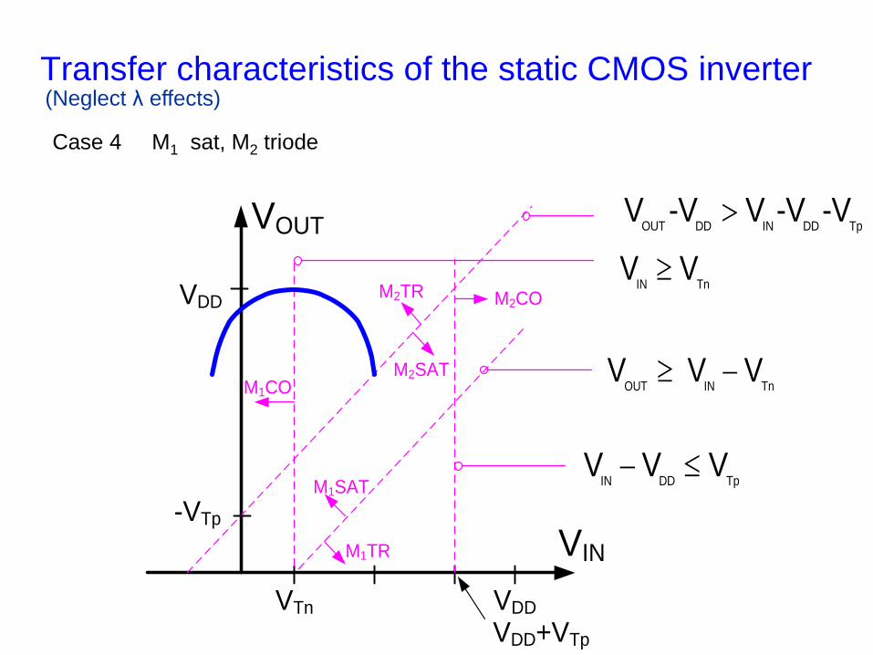
Case 4 M1 sat, M2 triode
VDD
VDD
VIN
VOUT
-VTp
VTn
VDD+VTp
M2CO
M1CO
M1TR
M2TR
M2SAT
M1SAT
(Neglect λ effects)
Transfer characteristics of the static CMOS inverter
M1
M2
VDD
VINVOUT
Case 4 M1 sat, M2 triode
2
2n OXn 1
D1 IN Tn
1
μ C WI V V
L
GS1 Tn DS1 GS1 TnV V V V V
GS2 Tp DS2 GS2 T2V V V V -V
Equating ID1 and –ID2 we obtain:
valid for:
IN Tn OUT IN TnV V V V V
IN DD Tp OUT DD IN DD TpV V V V -V V -V -V
thus, valid for:
2
OUT DD2
D2 p OXp IN DD Tp OUT DD
2
V -VWI μ C V V V V -V
L
2
2 2n OXn OUT DD1 2
IN Tn p OXp IN DD Tp OUT DD
1 2
μ C V -VW WV V μ C V V V V -V
L L
(Neglect λ effects)
Transfer characteristics of the static CMOS inverter
Case 4 M1 sat, M2 triode
VDD
VDD
VIN
VOUT
-VTp
VTn
VDD+VTp
M2CO
M1CO
M1TR
M2TR
M2SAT
M1SAT
IN TnV V
OUT IN TnV V V
IN DD TpV V V
OUT DD IN DD TpV -V V -V -V
(Neglect λ effects)

Transfer characteristics of the static CMOS inverter
Case 4 M1 sat, M2 triode
VDD
VDD
VIN
VOUT
-VTp
VTn
VDD+VTp
M2CO
M1CO
M1TR
M2TR
M2SAT
M1SAT
IN TnV V
OUT IN TnV V V
IN DD TpV V V
OUT DD IN DD TpV -V V -V -V
(Neglect λ effects)

Transfer characteristics of the static CMOS inverter
VDD
VDD
VIN
VOUT
-VTp
VTn
VDD+VTp
Case 1Case 2
Case 3
Case 4
Partial solution:
(Neglect λ effects)
Transfer characteristics of the static CMOS inverter
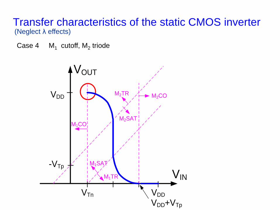
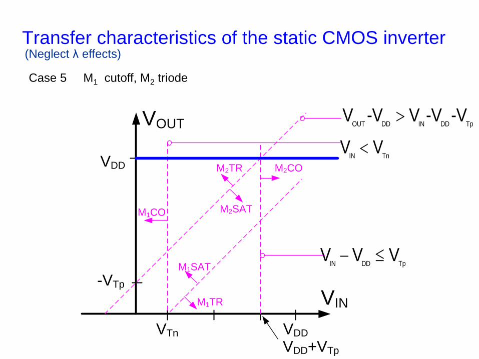
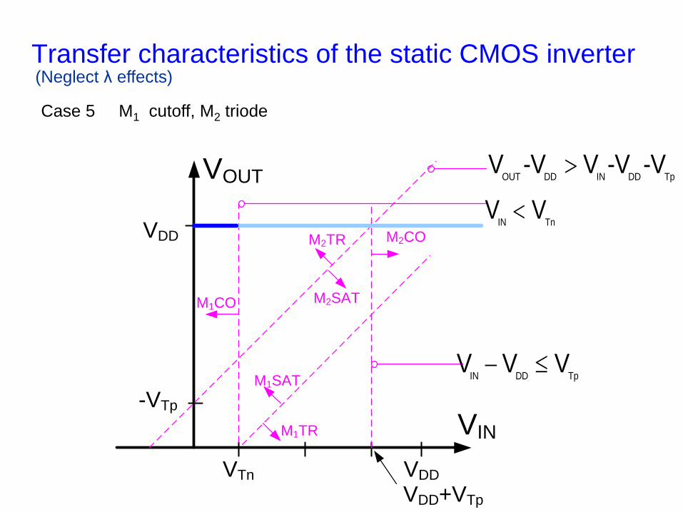
Case 4 M1 cutoff, M2 triode
VDD
VDD
VIN
VOUT
-VTp
VTn
VDD+VTp
M2CO
M1CO
M1TR
M2TR
M2SAT
M1SAT
(Neglect λ effects)
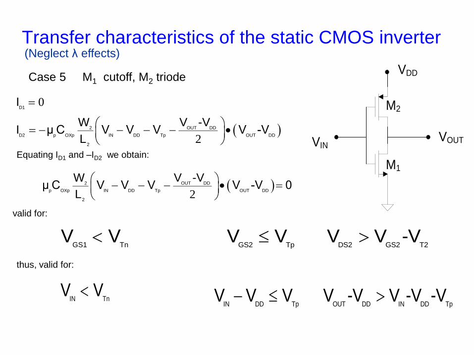
Transfer characteristics of the static CMOS inverter
M1
M2
VDD
VINVOUT
Case 5 M1 cutoff, M2 triode
0D1I
GS1 TnV V
GS2 Tp DS2 GS2 T2V V V V -V
Equating ID1 and –ID2 we obtain:
valid for:
IN TnV V
IN DD Tp OUT DD IN DD TpV V V V -V V -V -V
thus, valid for:
2
OUT DD2
D2 p OXp IN DD Tp OUT DD
2
V -VWI μ C V V V V -V
L
2
OUT DD2
p OXp IN DD Tp OUT DD
2
V -VWμ C V V V V -V 0
L
(Neglect λ effects)
Transfer characteristics of the static CMOS inverter
Case 5 M1 cutoff, M2 triode
VDD
VDD
VIN
VOUT
-VTp
VTn
VDD+VTp
M2CO
M1CO
M1TR
M2TR
M2SAT
M1SAT
IN TnV V
IN DD TpV V V
OUT DD IN DD TpV -V V -V -V
(Neglect λ effects)
Transfer characteristics of the static CMOS inverter
Case 5 M1 cutoff, M2 triode
VDD
VDD
VIN
VOUT
-VTp
VTn
VDD+VTp
M2CO
M1CO
M1TR
M2TR
M2SAT
M1SAT
IN TnV V
IN DD TpV V V
OUT DD IN DD TpV -V V -V -V
(Neglect λ effects)
Transfer characteristics of the static CMOS inverter
VDD
VDD
VIN
VOUT
-VTp
VTn
VDD+VTp
Case 1Case 2
Case 3
Case 4
Case 5
(Neglect λ effects)
M1
M2
VDD
VINVOUT

Transfer characteristics of the static CMOS inverter
VDD
VDD
VIN
VOUT
-VTp
VTn
VDD+VTp
(Neglect λ effects)
Transfer characteristics of the static CMOS inverter
VDD
VDD
VIN
VOUT
-VTp
VTn
VDD+VTp
VTRIP
1
1
(Neglect λ effects)
1
p 2 1
Tn DD Tp
n 1 2
IN
p 2 1
n 1 2
μ W LV V +V
μ W LV
μ W L
μ W L
From Case 3 analysis:
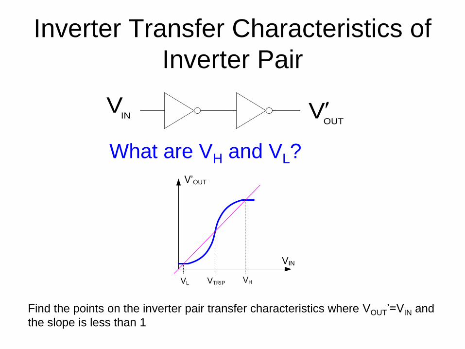
Inverter Transfer Characteristics of
Inverter Pair
INV
OUTV
What are VH and VL?
Find the points on the inverter pair transfer characteristics where VOUT’=VIN and
the slope is less than 1
V’OUT
VIN
VL VHVTRIP
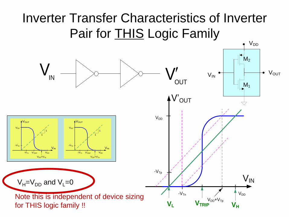
Inverter Transfer Characteristics of Inverter
Pair for THIS Logic Family
INV
OUTV
VDD
VDD
VIN
VOUT
-VTp
-VTn
VDD+VTp
VTRIP
1
1
VDD
VDD
VIN
VOUT
-VTp
-VTn
VDD+VTp
VTRIP
1
1
VDD
VDD
VIN
V’OUT
-VTp
-VTn
VDD+VTp
VL VHVTRIP
VH=VDD and VL=0
Note this is independent of device sizing
for THIS logic family !!
M1
M2
VDD
VINVOUT

Sizing of the Basic CMOS Inverter
M1
M2
VDD
VINVOUT
How should M1 and M2 be sized?
How many degrees of freedom are there in the design of the inverter?
The characteristic that device sizes do not need to be used to
establish VH and VL logic levels is a major advantage of this type of
logic
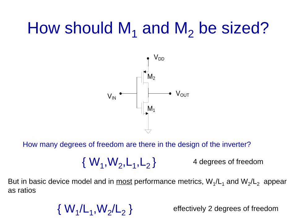
How should M1 and M2 be sized?
M1
M2
VDD
VINVOUT
How many degrees of freedom are there in the design of the inverter?
{ W1,W2,L1,L2 } 4 degrees of freedom
But in basic device model and in most performance metrics, W1/L1 and W2/L2 appear
as ratios
{ W1/L1,W2/L2 } effectively 2 degrees of freedom

How should M1 and M2 be sized?
M1
M2
VDD
VINVOUT
{ W1,W2,L1,L2 } 4 degrees of freedom
How are W1 and W2 chosen?
{ W1,W2} effectively 2 degrees of freedom
Usually pick L1=L2=Lmin
Depends upon what performance parameters are most important for a given
application!

How should M1 and M2 be sized?
M1
M2
VDD
VINVOUT
One popular sizing strategy:
1. Pick W1=WMIN to minimize area of M1
2. Pick W2 to set trip-point at VDD/2
pick L1=L2=Lmin
VDD
VDD
VIN
VOUT
-VTp
VTn
VDD+VTp
VTRIP
1
1
1
p 2
Tn DD Tp
n 1
OUT IN TRIP
p 2
n 1
μ WV V +V
μ WV =V V
μ W
μ W
Observe Case 3 provides expression for VTRIP
Thus, at the trip point,
2n
p
DD 2
1
μV W, if
W μ
End of Lecture 36


