Updated By: Robert Buckley Page 1 of 23 Updated: 12/21/2017 EE 330 Spring 2018 Lab 1: Cadence® Custom IC design tools – Setup, Schematic capture and simulation Table of Contents Objective.......................................................................................................................................... 2 1. Setup............................................................................................................................................ 2 Set Bash Shell for the account .................................................................................................... 2 2. Starting Cadence Custom IC tool and creating libraries .............................................................. 3 Creating a new library ................................................................................................................. 5 Creating a new cell and a cell view ............................................................................................. 7 3. Schematic Capture....................................................................................................................... 9 Instantiating the components ..................................................................................................... 9 Connecting the components ..................................................................................................... 11 Adding labels ............................................................................................................................. 11 Editing object properties........................................................................................................... 12 Adding comments ..................................................................................................................... 13 4. Simulating a circuit .................................................................................................................... 14 Setting up the simulations ........................................................................................................ 14 Setting up the outputs .............................................................................................................. 15 Running the simulation and viewing the results....................................................................... 15 5: Inverter Simulation with Verilog HDL inside ModelSim ............................................................ 16
Transcript
Updated By: Robert Buckley Page 1 of 23 Updated: 12/21/2017
EE 330 Spring 2018 Lab 1: Cadence® Custom IC design tools – Setup, Schematic capture and simulation
Table of Contents Objective.......................................................................................................................................... 2
Set Bash Shell for the account Bash shell is normally the default shell, so this step is normally unnecessary. So first you
should check what shell your terminal is using. To do this open the terminal and use the command echo $0
The ‘echo’ command will print whatever you type after it to the terminal. If you type ‘echo hello world’ it will type “hello world” as the output in the terminal. By adding a ‘$’ in front of something it becomes a variable, which can be set in scripts or on the terminal with other commands. The variable ‘$0’ is the shell you are currently using. If the output is not
bash
You will need to follow these steps, Login to http://www.asw.iastate.edu Click on: Manage user “Net-ID” Click on: Set your login shell (Unix/Linux) Select: “/bin/bash” Click on: Update Shell Click on: logout
Updated By: Robert Buckley Page 4 of 23 Updated: 12/21/2017
Note: As discussed above, when you type a program name into the terminal it starts the
program. ‘virtuoso’ is aliased to the full path name to the program. The ‘&’ after the command
means that the program is opened in the background, so you can still use the terminal you
opened it in for other commands. If you want to see the full path name used when you use the
command use,
which virtuoso
The ‘which’ command looks through the filesystem to inform you what version of a program you
are using and where it is.
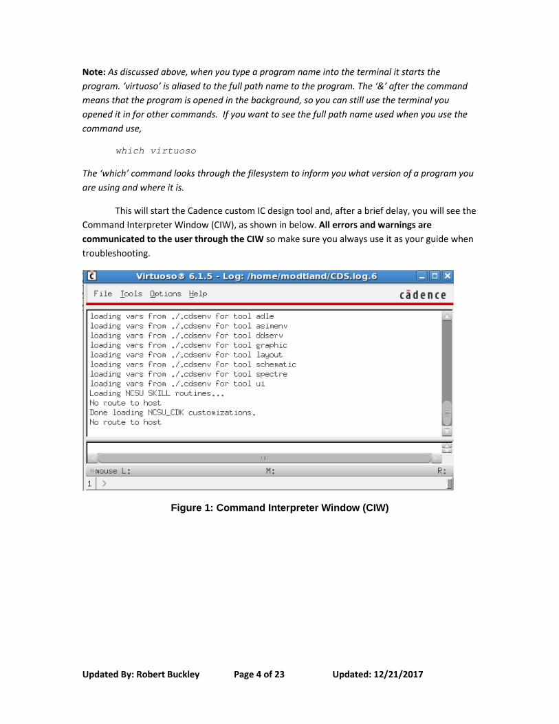
This will start the Cadence custom IC design tool and, after a brief delay, you will see the
Command Interpreter Window (CIW), as shown in below. All errors and warnings are
communicated to the user through the CIW so make sure you always use it as your guide when
troubleshooting.
Figure 1: Command Interpreter Window (CIW)
Updated By: Robert Buckley Page 5 of 23 Updated: 12/21/2017
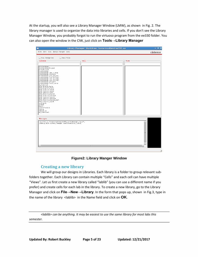
At the startup, you will also see a Library Manager Window (LMW), as shown in Fig. 2. The
library manager is used to organize the data into libraries and cells. If you don't see the Library
Manager Window, you probably forgot to run the virtuoso program from the ee330 folder. You
can also open the window in the CIW, just click on Tools→Library Manager
Figure2: Library Manger Window
Creating a new library We will group our designs in Libraries. Each library is a folder to group relevant sub-
folders together. Each Library can contain multiple “Cells” and each cell can have multiple
“Views”. Let us first create a new library called “lablib” (you can use a different name if you
prefer) and create cells for each lab in the library. To create a new library, go to the Library
Manager and click on File→New→Library. In the form that pops up, shown in Fig.3, type in
the name of the library <lablib> in the Name field and click on OK.
<lablib> can be anything. It may be easiest to use the same library for most labs this
semester.
Updated By: Robert Buckley Page 6 of 23 Updated: 12/21/2017
Figure 3 : Form to create a new library
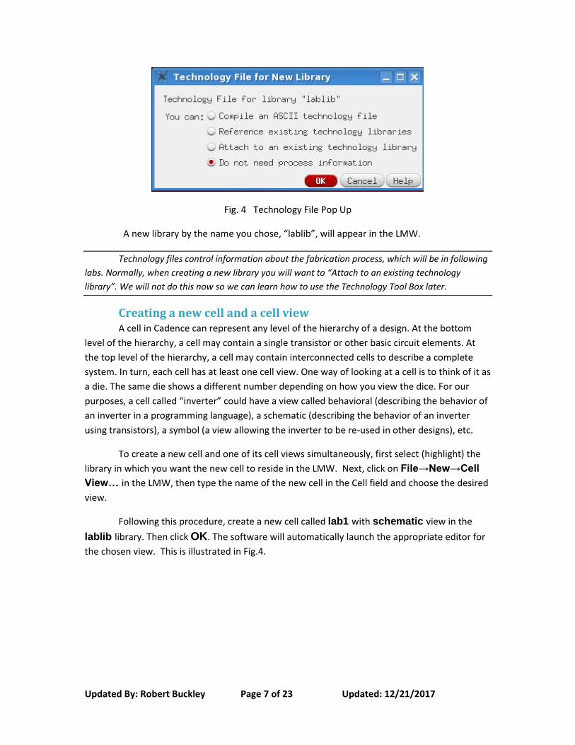
A Technology File window will pop up. For the library you just created, select “Do not need
process information” as shown in Fig. 4 and then click OK.
Updated By: Robert Buckley Page 7 of 23 Updated: 12/21/2017
Fig. 4 Technology File Pop Up
A new library by the name you chose, “lablib”, will appear in the LMW.
Technology files control information about the fabrication process, which will be in following
labs. Normally, when creating a new library you will want to “Attach to an existing technology
library”. We will not do this now so we can learn how to use the Technology Tool Box later.
Creating a new cell and a cell view A cell in Cadence can represent any level of the hierarchy of a design. At the bottom
level of the hierarchy, a cell may contain a single transistor or other basic circuit elements. At
the top level of the hierarchy, a cell may contain interconnected cells to describe a complete
system. In turn, each cell has at least one cell view. One way of looking at a cell is to think of it as
a die. The same die shows a different number depending on how you view the dice. For our
purposes, a cell called “inverter” could have a view called behavioral (describing the behavior of
an inverter in a programming language), a schematic (describing the behavior of an inverter
using transistors), a symbol (a view allowing the inverter to be re-used in other designs), etc.
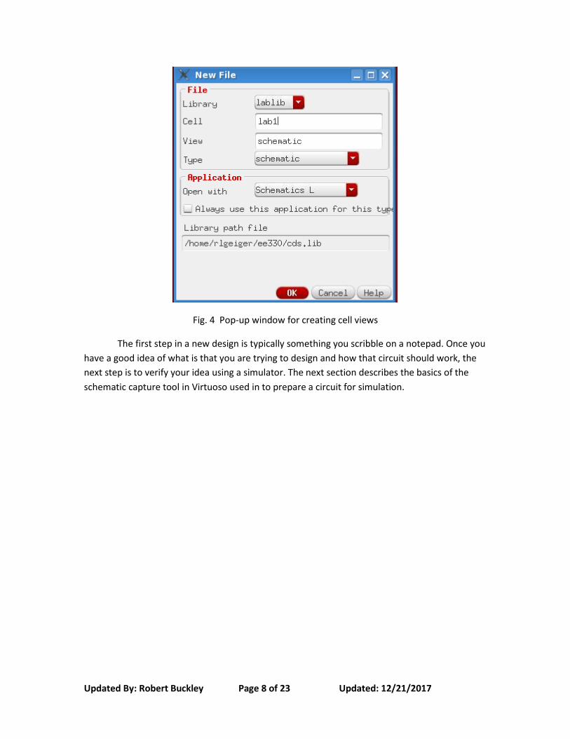
To create a new cell and one of its cell views simultaneously, first select (highlight) the
library in which you want the new cell to reside in the LMW. Next, click on File→New→Cell
View… in the LMW, then type the name of the new cell in the Cell field and choose the desired
view.
Following this procedure, create a new cell called lab1 with schematic view in the
lablib library. Then click OK. The software will automatically launch the appropriate editor for
the chosen view. This is illustrated in Fig.4.
Updated By: Robert Buckley Page 8 of 23 Updated: 12/21/2017
Fig. 4 Pop-up window for creating cell views
The first step in a new design is typically something you scribble on a notepad. Once you
have a good idea of what is that you are trying to design and how that circuit should work, the
next step is to verify your idea using a simulator. The next section describes the basics of the
schematic capture tool in Virtuoso used in to prepare a circuit for simulation.
Updated By: Robert Buckley Page 9 of 23 Updated: 12/21/2017
3. Schematic Capture To practice schematic capture, we will enter the circuit shown in the Pre-lab section.
You should already have the schematic editor window open editing the schematic view of the
cell lab1. The first step is to instantiate all the required components.
Instantiating the components To place all the components in the schematic window, click on menu item
Create→Instance. You will see two windows popping up on the screen (shown below):
“Component browser” and “Add Instance”.
In the “Component Browser”, change the library to “analogLib” and click on “Flatten” to
see all the cells without categorization. Now find the resistor cell and click on it (The resistor cell
is called res). Notice how the “Add Instance” form changes to reflect the selection of resistor
with a default value of 1K. Change the value of the resistor to 10K. Do not click in the Schematic
window yet! Just move your cursor over an empty space in the schematic window. You will see a
yellow colored resistor “floating” with the cursor. If you click anywhere in the window, a copy of
the resistor will be placed. Try it. If you need a component at a different orientation, click on
“Rotate”, “Sideways”, or “Upside Down” in the “Add Instance” form.
You can use icons from the icon bar on the schematic window for common editing tasks.
Hover the mouse pointer over an icon to determine what it is. As practice, locate the “instance” icon.
Updated By: Robert Buckley Page 10 of 23 Updated: 12/21/2017
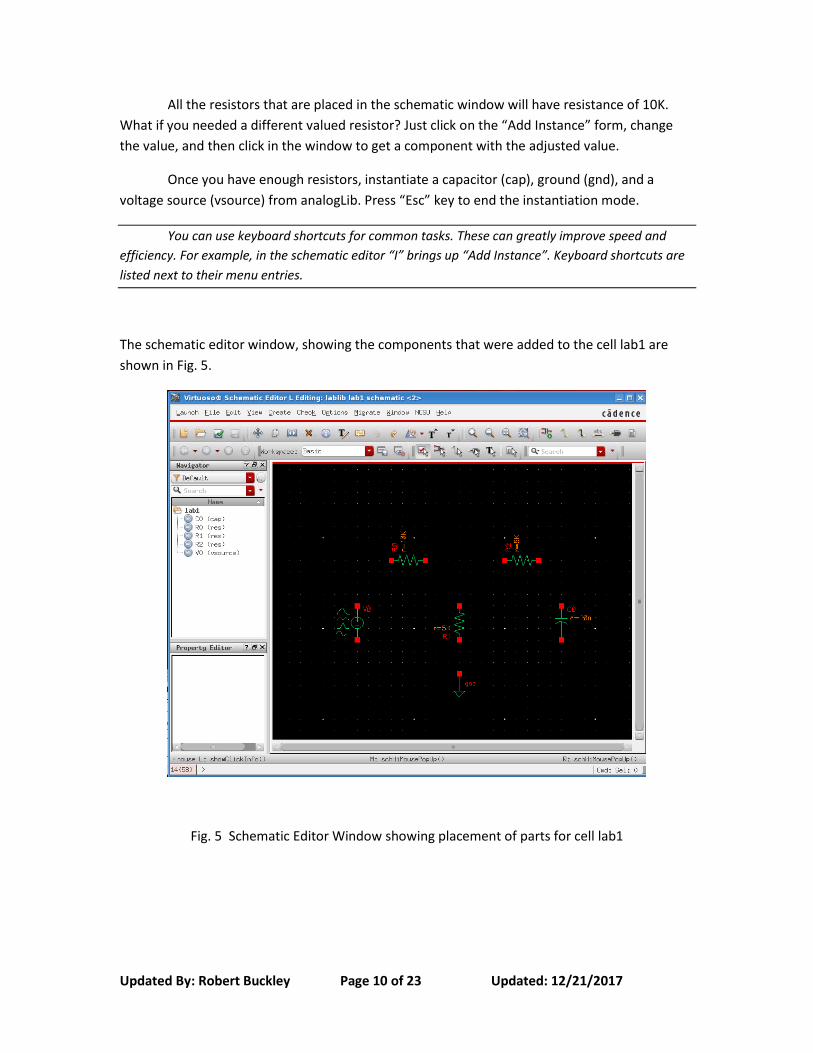
All the resistors that are placed in the schematic window will have resistance of 10K.
What if you needed a different valued resistor? Just click on the “Add Instance” form, change
the value, and then click in the window to get a component with the adjusted value.
Once you have enough resistors, instantiate a capacitor (cap), ground (gnd), and a
voltage source (vsource) from analogLib. Press “Esc” key to end the instantiation mode.
You can use keyboard shortcuts for common tasks. These can greatly improve speed and
efficiency. For example, in the schematic editor “I” brings up “Add Instance”. Keyboard shortcuts are
listed next to their menu entries.
The schematic editor window, showing the components that were added to the cell lab1 are
shown in Fig. 5.
Fig. 5 Schematic Editor Window showing placement of parts for cell lab1
Updated By: Robert Buckley Page 11 of 23 Updated: 12/21/2017
Connecting the components There are two ways to interconnect components. First, use the menu entry
Create→Wire (narrow) to get into the wiring mode (You could also have pressed the shortcut
“w” key or clicked on the Add-Wire (narrow) icon). When in wiring mode, click on the red
terminal of a component to start one end of the wire (you do not need to keep the button
down). Now click on the other component’s terminal where you want the connection to
terminate. If you make a mistake and want to quit the wiring mode, press the “Escape” key on
the keyboard. You can undo the last action by pressing “u”.
The second way to add wiring is to first bring the mouse pointer over the red terminal of
a component’s terminal. While clicking and holding the mouse button, drag you mouse and you
will see a wire started. You can let go of the button now and the wiring will continue. Hit
“Escape” anytime to cancel. Unlike the first method, the wiring mode automatically terminates
with the completion of one connection.
Complete wiring the circuit. To make sure there are no floating components or
connection problems, we need to “Check and Save” the design. Click on the icon or the “Check
and Save” entry from the “File” menu. Check the CIW window to make sure the design was
saved without errors.
Adding labels As you wire the components together, every net is automatically assigned a name such
as net1, net2, etc. These names are fine for the software but are not easy for us to remember.
Adding labels to wires helps us to interact with the tools more efficiently. To add a label to a
wire, click on the menu item Create→Wire Name (or use shortcut “l”). In the form, type vIn
vMid vOut. Bring your mouse pointer into the schematic window. If you do not see the
“floating” vIn attached to your cursor, you first need to click on the title bar of the schematic
window to make it active. Now you should see the vIn attached to the mouse pointer. Click your
mouse pointer on the net you wish to call vIn. Note how the next label from the list you typed in
the form appears once you have placed the first label. This is a convenient way of adding
multiple labels without having to go back and forth between the form and the schematic
window.
Labels provide functionality in addition to being visual aids: connectivity. If two
unconnected nets have the same name, they are considered to be electrically connected. This
feature can allow you to create schematics with less clutter but can also be a source of mistakes.
Use the capability of labels to create connectivity judiciously or your schematics may actually
become less readable.
Updated By: Robert Buckley Page 12 of 23 Updated: 12/21/2017
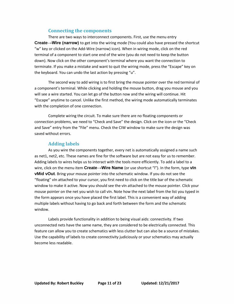
Fig. 6 Schematic showing interconnected components and net labels
Editing object properties What if you made a typing mistake when creating labels or need to modify the value of
a component? You can make the required changes by clicking on the object to select it and then
clicking Edit→Properties→Objects (find the shortcut for this if you don’t want to click three
menu levels every time!).
For practice, let us modify the properties of the voltage source component, vsource. The
vsource component is capable of generating a variety of stimuli.
Tip: It is possible, and often perferable, to use other sources from analogLib, such as vdc
for dc only and vsin for sine waves. vsource has multiple options, so it is used here to be able to
switch between them easily.
Bring up the properties form for vsource. In the next section, we will run dc, ac, and
transient simulations. For those simulations to work, we need to provide appropriate input
stimuli.
− For DC simulation, In the “DC voltage” box, type 1. This dc voltage is used to compute the
quiescent operating point of the circuit. Click on apply (at the top of the form). This is the input
for dc analysis.
− For ac analysis input, find the entry “Display small signal params” and turn the option on. The
form will update to display new form fields. Add 1V in the “AC magnitude. This input value will
be used for the AC analysis.
− For transient analysis, you need to choose the “Source type” field to the type you need. Enter
all the applicable entries and click on OK.
The vsource component is now configured for simulations. Click on “Check and save” to
save your design. Correct any errors or warnings before proceeding further.
Updated By: Robert Buckley Page 13 of 23 Updated: 12/21/2017
Always click “check and save” before running a simulation. Changing anything in
the schematic will make the simulation fail unless a “check and save” is run.
Save often. Cadence tools have a tendency to crash, although this occurs more
often with more complex designs. Using “save” instead of “check and save” will save
whatever you are currently working on without a pop-up box pointing out errors and
possibly not saving.
Adding comments It is good practice to add comments to the schematics. Click on
Create→Note→Text… and fill out the form. The comments are useful reminders to yourself
about the particular schematic and can also provide instructions for others if you share your
schematics.
Updated By: Robert Buckley Page 14 of 23 Updated: 12/21/2017
4. Simulating a circuit Once the schematic capture is complete, we can simulate the circuit to test if it
performs according to the design. To do this, we must first open the Analog Design Environment
(ADE) window. To open the ADE window, click on
Launch→ADE L
After opening the ADE window, go to
Setup → Simulator/Directory/Host
and set the Project Directory path to
/local/[username]/cadence/simulation
This way when you are running a simulation then the simulation data will be stored on
the /local/ rather than eating up your account space. It is also highly recommended to keep on
deleting the old simulation data from time to time so that everyone can have enough /local/
space.
The ADE window is used to select a simulator as well as set up all the options and
simulations for the simulator. The default simulator is in ADE is a simulator called Spectre from
Cadence. It has the same capabilities as Spice with enhancements introduced by Cadence. You
can choose a different simulator by clicking on Setup→Simulator/Directory/Host… menu
item. We will use Spectre for this lab and for most of our analog simulations.
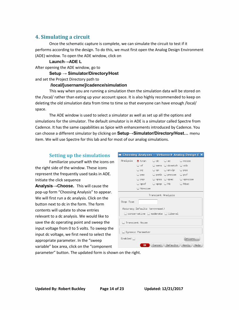
Setting up the simulations Familiarize yourself with the icons on
the right side of the window. These icons
represent the frequently used tasks in ADE.
Initiate the click sequence
Analysis→Choose. This will cause the
pop-up form “Choosing Analysis” to appear.
We will first run a dc analysis. Click on the
button next to dc in the form. The form
contents will update to show entries
relevant to a dc analysis. We would like to
save the dc operating point and sweep the
input voltage from 0 to 5 volts. To sweep the
input dc voltage, we first need to select the
appropriate parameter. In the “sweep
variable” box area, click on the “component
parameter” button. The updated form is shown on the right.
Updated By: Robert Buckley Page 15 of 23 Updated: 12/21/2017
To select the dc input voltage of the vsource, click on “Select component” and then click on
vsource in the schematics window. In the new form that pops up, click on the first entry, dc, to
choose the dc voltage of the vsource. You would follow a similar procedure to sweep other
parameter of a source, if desired.
Next, enter the range of sweep in the start and stop boxes. Click on Apply for all these
changes to take effect. This completes the dc analysis setup. Click OK to close the form and
return to ADE.
We did not specify a step size for the dc analysis. The step size is automatically chosen since
the “sweep type” is set to automatic. If the step size is too large you can chance the sweep type for
more finite control.
Setting up the outputs We need to tell the simulator which node voltages we are interested in plotting once
the simulation is complete. To choose which signals to plot, click on the menu item
Outputs→To be Plotted →Select on Schematics. The bottom of the ADE tells you to
select the outputs you want plotted. Clicking on a net or a label selects voltage of the net to be
plotted. Find the schematics window and click on the three labels we added earlier. Once done,
press the escape key to get out of this selection mode.
By default, only the voltages in the circuit are saved. To be able to save and plot waveform of
a current, click on Outputs->Save all… in ADE and turn on the option “selected” for “Save device
currents (currents)”. To plot the current flowing into a device terminal, click on the red terminal (red
square on components). If you see a circle around that terminal, the current will be plotted.
Running the simulation and viewing the results Now that we have set up which type of analysis we want to run and which outputs we
are interested in, let us run the simulation. Click on the green arrow icon to run the simulation.
Once the simulation is complete, a waveform viewer window will come up with the plots of the
outputs you selected in the previous step. Once again, familiarize yourself with the icons in the
waveform viewer for common operations you need to perform on the waveforms.
Updated By: Robert Buckley Page 16 of 23 Updated: 12/21/2017
5: ModelSim Introduction Throughout this course, we will be using Verilog to simulate and design digital circuits
and systems. This will be extremely useful in the final project, and will have a homework
question each week. Verilog is common simulation software for digital designers in industry and
has many features that will not be used in this class (EE 465 is the class to take if you are
interested in digital VLSI). Follow the steps below for running ModelSim, creating an inverter
behavioral file in Verilog HDL, creating a testbench, and finally running a simple simulation.
1. First, download ModelSim Environment Setup Script from the class website and place it in
the ‘Home’ (~/) directory. In a terminal, enter the command below to source the path of the
ModelSim software.
source ~/EE330ModelsimEnvironment.sh
Source will use the file you specify to attempt to extract information to be able to run another
program. Once the script finishes running, you can now run ModelSim by typing:
vsim &
At this point you should create a directory to hold all Verilog code you write for this class. We
suggest changing directory into ee330, “cd ~/ee330”, and running
mkdir verilog
‘mkdir’ is short for “make directory” and is how you create a directory in the terminal. Move to
this directory (cd verilog) and run the command to start modelsim (vsim &). This will save
work you do in your newly made verilog folder.
Updated By: Robert Buckley Page 17 of 23 Updated: 12/21/2017
2. Once ModelSim opens, the next step is to create a new project
• Click on File, then New, then choose Project on the drop down menu
• Enter your project name (this does not affect anything, “myVerilog” would work)
• Choose your project location (Use the directory created above, “~/ee330/verilog”)
• The default library name should be work.
• Click OK.
3. You will be asked if want to create the project directory.
• Click OK button
4. Next you will be presented with the Add Items to Project Dialog. While you can use this
dialog to create new source files or add existing ones, we will not be using this option for
this lab. We’ll add source files later so just click on the Close button
Updated By: Robert Buckley Page 18 of 23 Updated: 12/21/2017
5. You now have a project by the name of “myVerilog”.
6. Now we want to add a new file to our project.
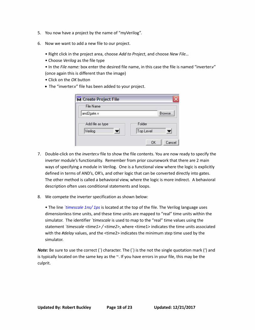
• Right click in the project area, choose Add to Project, and choose New File…
• Choose Verilog as the file type
• In the File name: box enter the desired file name, in this case the file is named “inverter.v”
(once again this is different than the image)
• Click on the OK button
The “inverter.v” file has been added to your project.
7. Double-click on the inverter.v file to show the file contents. You are now ready to specify the
inverter module’s functionality. Remember from prior coursework that there are 2 main
ways of specifying a module in Verilog. One is a functional view where the logic is explicitly
defined in terms of AND’s, OR’s, and other logic that can be converted directly into gates.
The other method is called a behavioral view, where the logic is more indirect. A behavioral
description often uses conditional statements and loops.
8. We compete the inverter specification as shown below:
• The line `timescale 1ns/ 1ps is located at the top of the file. The Verilog language uses
dimensionless time units, and these time units are mapped to “real” time units within the
simulator. The identifier `timescale is used to map to the “real” time values using the
statement `timescale <time1> / <time2>, where <time1> indicates the time units associated
with the #delay values, and the <time2> indicates the minimum step time used by the
simulator.
Note: Be sure to use the correct (`) character. The (`) is the not the single quotation mark (‘) and
is typically located on the same key as the ~. If you have errors in your file, this may be the
culprit.
Updated By: Robert Buckley Page 19 of 23 Updated: 12/21/2017
• The inverter module is also declared using module inverter(); and endmodule, but the ports
are left for us to define.
• Be sure to save the changes to the inverter.v file by clicking on File and choosing Save.
`timescale 1ns/1ps
module inverter (Vin, Vout);
input Vin;
output Vout;
wire Vout;
assign Vout = ~Vin;
endmodule
9. We also want to add a testbench and again follow Steps 6 – 8 to add “inverter_tb.v”. Then
we add the functionality of the testbench module as shown below.
`timescale 1ns/1ps
module inverter_tb();
reg A;
wire B;
inverter inv( .Vin(A), .Vout(B) );
initial
begin
A = 1'b0;
end
always
#20 A <= ~A;
endmodule
Updated By: Robert Buckley Page 20 of 23 Updated: 12/21/2017
Code Explained
`timescale 1ns/1ps : sets how long an operation lasts. This is used later in the #20 A <= ~A line, which means every 20 timescale interval set A to equal not A.
module [Name](Parameters); the [Name] is the actual name of the device, to be referenced by other devices. The Parameters are all inputs and outputs, things that can be accessed by other devices.
Input Vin; Defines Vin as an input, which means another Verilog module can control what this is.
output Vout; Defines Vin as an output, which means another Verilog module can use it as an input.
wire Vout; Defines Vout as a wire in adition to an output. This allows it to work with the assign statement.
assign Vout = ~Vin; This sets Vout to equal not Vin at all times. reg A; This sets A as a register, which means it can be controlled using statements
later, such as; initial
begin
A = 1'b0;
end : initial sets the initial state of things inside of it, in this case the register A being
set to 0. Because A is 1 bit long A = [bits]’b[inary]0, if A were 4 bits it would be A = 4’b0000.
The ‘begin’ and ‘end’ work like parenthesize in other programs, they allow multiple lines to
be controlled by the ‘initial’ above. always
#20 A <= ~A; always@(event) causes what is inside the always statement to
occure when the event occurs. always@(posedge Clock) will cause whatever is in it to happen
when a signal called Clock becomes positive from negative. If ‘always’ has no @ statement it
happens whenever any signal changes in the code. The #20 A <= ~A means every 20
timescales A becomes not A (10, 01).
Endmodule : designates the end of the program.
Notice that the inputs of the inverter module are now defined differently. The inputs of inverter.v are given values (like applying a bias from a voltage source on a real test bench to a circuit on a breadboard) and the outputs are observed to see if they match expectations. More detailed testbenches can be written and the skill of writing good testbenches is heavily desired. Often the testbench takes longer to write and requires more skill than the actual module, and thus a good testbench will be thorough but efficient to reduce wasted resources. 10. After saving both “inverter.v” and “inverter_tb.v”, we want to check the syntax of both files.
• Click on the Compile Menu and select Compile All
• If the syntax was correct, a checkmark will appear next to each file
• If the syntax was incorrect, the window at the bottom will list the individual errors.
11. Now it’s time to simulate the design.
• Click on the Simulate menu and choose Start Simulation
• Expand the selection for the work library by click on the + symbol on the left.
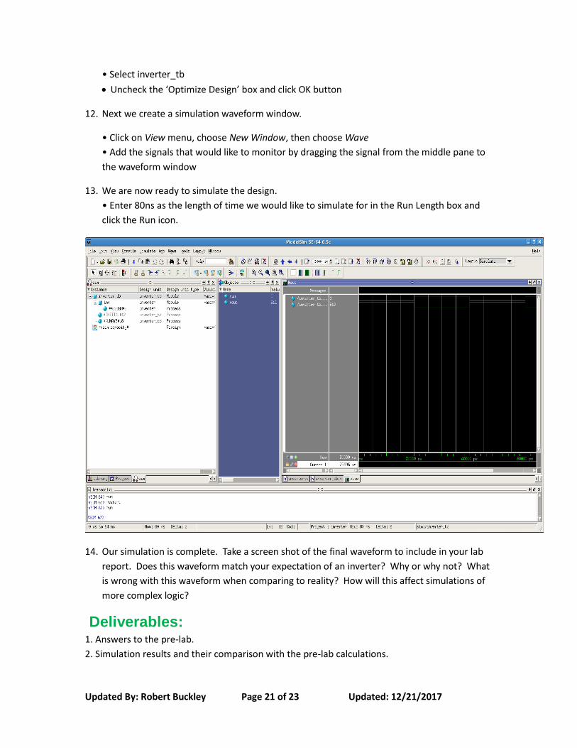
Updated By: Robert Buckley Page 21 of 23 Updated: 12/21/2017
• Select inverter_tb
Uncheck the ‘Optimize Design’ box and click OK button
12. Next we create a simulation waveform window.
• Click on View menu, choose New Window, then choose Wave
• Add the signals that would like to monitor by dragging the signal from the middle pane to
the waveform window
13. We are now ready to simulate the design.
• Enter 80ns as the length of time we would like to simulate for in the Run Length box and
click the Run icon.
14. Our simulation is complete. Take a screen shot of the final waveform to include in your lab
report. Does this waveform match your expectation of an inverter? Why or why not? What
is wrong with this waveform when comparing to reality? How will this affect simulations of
more complex logic?
Deliverables: 1. Answers to the pre-lab.
2. Simulation results and their comparison with the pre-lab calculations.
Updated By: Robert Buckley Page 22 of 23 Updated: 12/21/2017
Appendix A: Basic UNIX commands
This appendix introduces some basic commonly used UNIX commands. The following
notation is used: words in the fixed width font are commands you need to type exactly,
words in the italic font are to be substituted with appropriate words for your intended purpose,
and words within square brackets [ ] are optional. Unix command as well as file names are case-
sensitive.
gedit filename
Opens the file filename if it exists. If the file filename does not exist, a new file
by that name is created. Instead of gedit, you can use any text editor of your choice.
Some popular editors include vi, pico, emacs, etc.
ls -l [ directory ]
Lists the contents of the directory. If no directory name is supplied, contents of the
current directory are listed.
cp source_file target_file
Copies the source_file to a new file named target_file.
mv old_filename new_filename
Moves/renames the old_filename to new_filename. If the target new_filename includes
a path, the file is renamed and moved to that path. It can also be used to rename
directory.
rm trash_file
Removes/deletes the unwanted trash_file. Note that file removed cannot be
"undeleted", so make sure you know what you are going to delete.
mkdir new_directory
Makes a new subdirectory named new_directory within the current directory.
cd [directory]
Change current directory to the given directory. If no directory name is provided, the
current directory will change to user's home directory.
pwd
Shows the present working directory
Updated By: Robert Buckley Page 23 of 23 Updated: 12/21/2017
rmdir trash_directory
Remove/delete the unwanted trash_directory.
man command
Show the manual of the command. You can learn more detail about any given command
using man, e.g. man ls shows all available options and functionalities for ls
command.
more filename
Shows the contents of a file one screen at a time.
ps
Shows the currently running processes.
A couple of useful special symbols
~
The symbol ~ is used to denote the user’s home directory. If the complete path of the
home directory happens to be / home/username/ , then using ~ represents that
complete string. For example, if you want to look at the contents of a file in your home
directory, the following commands produce the same result
more /home/username/myfile
more ~/myfile
&
When launching a program that opens in a new window, placing an “&” at the end of
the command line allows the user to keep access to the command line, i.e., the “&”
instructs the program to run in the background.
These are just a few shell commands you need to know to get started. You are encouraged and
advised to learn other UNIX commands on your own, as they will increase your productivity, i.e.,