28
© Mark Redekopp, All rights reserved EE 357 Unit 10a (Embedded) Systems Programming Overview

© Mark Redekopp, All rights reserved
EE 357 Unit 10a
(Embedded) Systems Programming
Overview

© Mark Redekopp, All rights reserved
System Programming Issues
• Embedded systems programming have different design
requirements than general purpose computers like PC‟s
– I/O – Electro-mechanical devices, communication devices, etc.
– Real-Time systems – Calculations need to be able to keep pace
with inputs / outputs
• Hard Real Time – Must meet timing or computation is pointless– Anti-lock Braking System
• Soft Real Time – Should usually meet timing– MPEG/MP3 decoding can lose a sample or frame occasionally
– Limited Memory – Limited data and program memory sizes
– Reliability – Embedded software is hard to update
– Power Modes – Often allow programmer to put processor or
components into low-power mode
– Tool Chain – Development for target system on a host PC

© Mark Redekopp, All rights reserved
Embedded Devel. Tool Chain
• Develop code, using cross-platform
development tools (compiler, etc.) on host PC
• Download and run on target system
• Ethernet or serial connection to host PC for
debugger output
Ethernet or serial
debug connection
Actual
embedded
system I/O
Intel/AMD Platform
Coldfire Platform

© Mark Redekopp, All rights reserved
System Board
Multi-chip system vs. Microcontrollers (µC)
• Embedded systems often include a few chips
on a single board (proc., mem., I/O chip)
• Microcontroller combines processor, RAM,
Program ROM (usually FLASH), and I/O all on
a single chipsingle chipSingle Chip (uC)
Processor
RAM
ROM(Program
Store)
I/O Pins
I/O Pins(Timers,
Serial
Port, etc.)
General Purpose I/O pins
can control a wide variety
of sensors, actuators,
displays, etc.
Proc. +
Custom
Logic
RAM
I/O Interface
Chip
System Bus
(Addr., Data.,
Ctrl.)

© Mark Redekopp, All rights reserved
Embedded Processor Vendors
• Freescale (formerly Motorola)– HC08 Line (8-bit Microcontrollers)
• Inexpensive, low end (4 KB of ROM / 256 bytes RAM)
– Coldfire/68K (32-bit Microcontrollers)• Higher clock rates
• 512 KB FLASH ROM / 64 KB RAM
• Uses 68000/Coldfire ISA
– PowerPC [PPC] (General Purpose Processor Core)• Can be licensed as IP for custom designs or purchase actual chips
• Microchip PIC Microcontrollers– Mid- to Low-End / Popular with Hobbyists
• Atmel– High performance, RISC core microcontrollers
• ARM– License their processor cores to other design companies
– Very popular in commercial products (used in Apple‟s iPOD, etc.)

© Mark Redekopp, All rights reserved
MCF 52259 Core
• Coldfire V2 Core with ISA_A
• 8 MHz bus clock
• Memory– 64 KB RAM: used to hold data variables
– 512 KB ROM: stores program code • Not like a PC where we have a hard drive
• Usually Flash EEPROM is used
• Integrated I/O

© Mark Redekopp, All rights reserved
Integrated I/O Peripherals
• General Purpose (GP) I/O pins
– Pins can be used to take digital inputs from other chips/buttons or produce digital outputs to chips/LEDs
• Serial Ports/UART‟s/USB
– Universal Asynchronous Receiver/Transmitter (RS-232) serial ports
– USB
• Analog-to-Digital Converts
– Convert on-board sensor values (voltages) to digital numbers that can be processed
• Pulse Width Modulation (PWM)
– Can modulate different frequency signals
– Essentially is a form of Digital-Analog Conversion (DAC)
• Timers
– Keep track of time and/or external events and generate interrupts
• IIC / SPI Serial Protocols
– Interchip serial (one-bit at a time) communications protocols
• Ethernet Controller

© Mark Redekopp, All rights reserved
Memory Map
• 512KB Flash ROM
• 64 KB RAM
• I/O Control/Status Registers
• Memory map is programmable
via Base Address Registers
(BAR‟s)
– FLASHBAR = FLASH start
address
– VBR = Vector Table start
address
– RAMBAR = RAM start addr.
– IPSBAR = I/O Peripherals
start addr.
© Mark Redekopp, All rights reserved
Programming I/O Peripherals
• All I/O peripherals use the bits in specific
control/status registers to control their operation
and provide feedback info to the system
– These registers are mapped to physical addresses in
the system address space
– We can use a pointer in C to access them
• Many I/O peripherals have the ability to generate
an interrupt on a specific event (timer done, data
transfer complete, etc.)
You MUST read, reference, then re-read the MCF52259 Reference You MUST read, reference, then re-read the MCF52259 Reference
Manual (posted on Blackboard). It describes and shows register
definitions for all I/O peripherals.
© Mark Redekopp, All rights reserved
MCF52259 I/O Pin Usage
• MCF52259 comes in a 144-pin package of
which 96 pins can be used for programmable I/O
– 96 pins are broken into groups called “ports”
• All pins can be used for “general purpose I/O”
(GPIO) or for an alternative integrated I/O
peripheral (ADC, UART, PWM, etc.)
– GPIO simply means we can use software to output a
binary value on a pin or to use the pin as an input and
read the binary value present at a pin
– Breakdown of pins to ports is based on the alternate
integrated I/O function

© Mark Redekopp, All rights reserved
Alternate Port/Pin Functions
• Port DD[7:0]
• Port TA[3:0]
– Input Capture Timers
– PWM
• Port TD[3:0]
– PWM
• Port TC[3:0]
– DMA Timers
– PWM
• Port TE,TF,TG[7:0]
– Mini-FlexBus
• Port UA[3:0], UB[3:0],
UC[3:0]
– UART Port A, B, C
• Port AN[7:0]
– Analog to Digital
• Port NQ[7,5,3,1]
– External Interrupts
• Port AS[1:0], QS[6:5,3:0]
– IIC, QSPI
• Port TI,TJ,TH[7:0]
– Ethernet, USB

© Mark Redekopp, All rights reserved
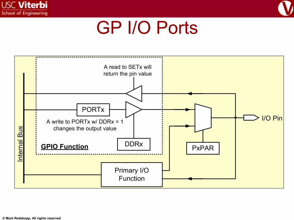
GP I/O Ports
• Pins can be used for their primary I/O function (A-to-D,
UART, etc.) or as GPIO
• GPIO allows pins to be used as programmable digital
inputs and outputs– Outputs: Can connect pin to drive other digital circuits
– Inputs: Can read current values of pins to control your software
• Control Registers– Pin Assignment Register (PxxPAR): 1 = Primary Function / 0 = GPIO
– Data Direction Register (DDRxx): 1 = Output / 0 = Input
– Port Data Register (PORTxx): Data to be output to pins if used as GPIO
output
– SETxx: Address used to read pin values

© Mark Redekopp, All rights reserved
GPIO Registers
Full 8-bit Ports Less-Than 8-bit Ports
Port xx Reg. (PORTAN)
If output, data bits to be placed on I/O
pins
PORT
xx7
PORT
xx6
PORT
xx5
PORT
xx4
PORT
xx3
PORT
xx2
PORT
xx0
PORT
xx1
PORT
xx3
PORT
xx2
PORT
xx0
PORT
xx1
Port xx Reg. (PORTTC)
If output, data bits to be placed on I/O
pins
DDR XX Reg. (DDRAN)
1 = Output, 0 = Input
DDRx
x7
DDRx
x6
DDRx
x5
DDRx
x4
DDRx
x3
DDRx
x2
DDRx
x0
DDRx
x1
DDRx
x3
DDRx
x2
DDRx
x0
DDRx
x1
DDR xx Reg. (DDRTC)
1 = Output, 0 = Input
SET xx Reg. (SETAN)
(Read Only)
SETxx
7
SETxx
6
SETxx
5
SETxx
4
SETxx
3
SETxx
2
SETxx
0
SETxx
1
SETxx
3
SETxx
2
SETxx
0
SETxx
1
SET xx Reg. (SETTC)
(Read Only)
© Mark Redekopp, All rights reserved
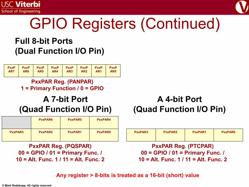
GPIO Registers (Continued)Full 8-bit Ports
(Dual Function I/O Pin)
PxxPAR Reg. (PANPAR)
1 = Primary Function / 0 = GPIO
PxxP
AR7
PxxP
AR6
PxxP
AR5
PxxP
AR4
PxxP
AR3
PxxP
AR2
PxxP
AR0
PxxP
AR1
A 7-bit Port
(Quad Function I/O Pin)
A 4-bit Port
(Quad Function I/O Pin)
PxxPAR Reg. (PQSPAR)
00 = GPIO / 01 = Primary Func. /
10 = Alt. Func. 1 / 11 = Alt. Func. 2
PxxPAR Reg. (PTCPAR)
00 = GPIO / 01 = Primary Func. /
10 = Alt. Func. 1 / 11 = Alt. Func. 2
PxxPAR6 PxxPAR5 PxxPAR4
PxxPAR3 PxxPAR2 PxxPAR1 PxxPAR0 PxxPAR3 PxxPAR2 PxxPAR1 PxxPAR0
Any register > 8-bits is treated as a 16-bit (short) value
© Mark Redekopp, All rights reserved
GP I/O Ports
DDRx
PORTx
I/O Pin
Inte
rna
l B
us
PxPAR
Primary I/O
Function
GPIO Function
A read to SETx will
return the pin value
A write to PORTx w/ DDRx = 1
changes the output value

© Mark Redekopp, All rights reserved
Programming GPIO
• At initialization…
– Set PxxPAR registers to
appropriate function (i.e.
GPIO)
– Set DDRxx registers for
appropriate direction
• During program
execution…
– Outputs: Assign values to
PORTxx registers
– Inputs: Use SETxx as an
input value in a statement
void main()
{
int x;
MCF_GPIO_PTCPAR = 0x00;
MCF_GPIO_PNQPAR = 0x00;
MCF_GPIO_DDRTC = 0x0f;
MCF_GPIO_DDRNQ = 0x00;
while (1){
x = MCF_GPIO_SETNQ & 0x80;
if(x != 0)
MCF_GPIO_PORTTC = 0x0a;
else
MCF_GPIO_PORTTC = 0x05;
}
}
A single push-button connected to
port NQ[7] and 4 LED‟s connected
to port TC[3:0]
© Mark Redekopp, All rights reserved
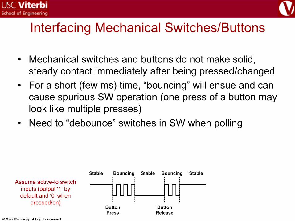
Interfacing Mechanical Switches/Buttons
• Mechanical switches and buttons do not make solid,
steady contact immediately after being pressed/changed
• For a short (few ms) time, “bouncing” will ensue and can
cause spurious SW operation (one press of a button may
look like multiple presses)
• Need to “debounce” switches in SW when polling
Stable Bouncing Stable Bouncing Stable
Button
Press
Button
Release
Assume active-lo switch
inputs (output „1‟ by
default and „0‟ when
pressed/on)

© Mark Redekopp, All rights reserved
C Preprocessor
• Before compilation of your code, the
preprocessor makes a pass through
your code looking for and handling
compiler directives such as #include
and #define (similar to how the
assembler converts assembler
directives)
– #include “source_file”
• Inserts “source_file” at that point in the code
– #define is used to define macros
(find/replace patterns)
Preprocessor
Compiler
Assembler
Linker
© Mark Redekopp, All rights reserved
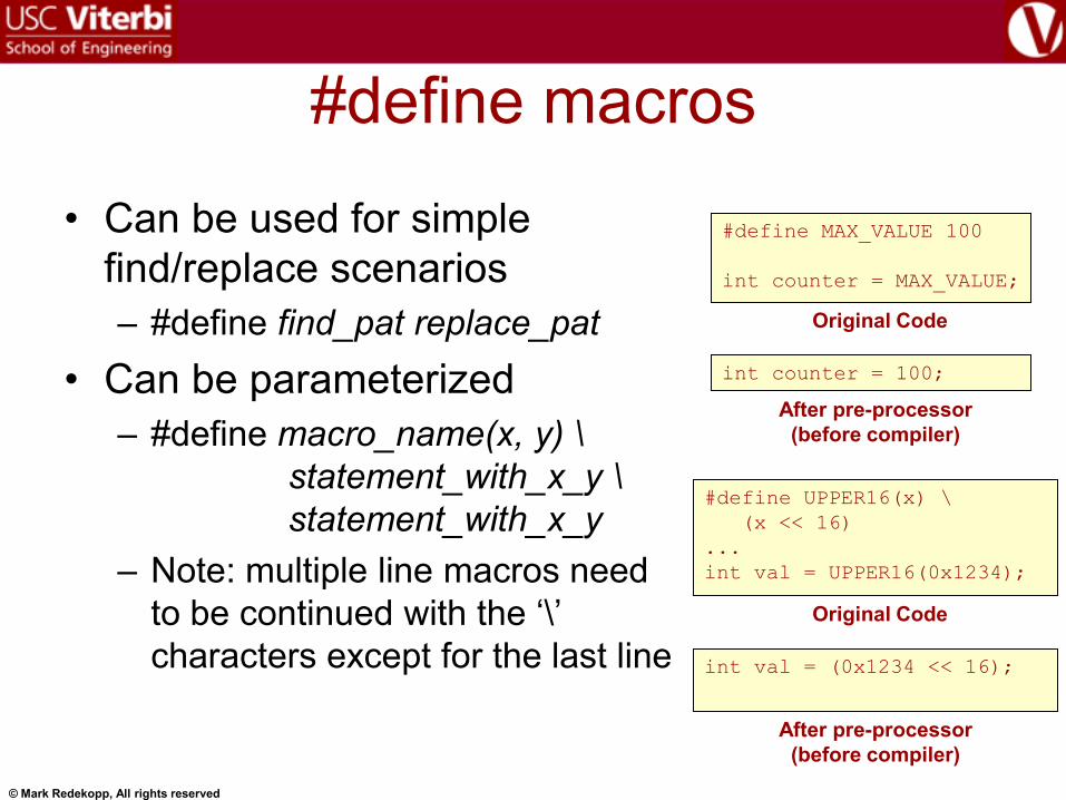
#define macros
• Can be used for simple
find/replace scenarios
– #define find_pat replace_pat
• Can be parameterized
– #define macro_name(x, y) \
statement_with_x_y \
statement_with_x_y
– Note: multiple line macros need
to be continued with the „\‟
characters except for the last line
#define MAX_VALUE 100
int counter = MAX_VALUE;
int counter = 100;
Original Code
After pre-processor
(before compiler)
#define UPPER16(x) \
(x << 16)
...
int val = UPPER16(0x1234);
int val = (0x1234 << 16);
Original Code
After pre-processor
(before compiler)

© Mark Redekopp, All rights reserved
Pointers
• A variable that holds the
address (pointer) to
another variable
– „*‟ in declaration indicates
you want a pointer
– „*‟ in code indicates you
want the value pointed to
by the pointer
– „&‟ evaluates to the
address of a variable
int x = 5;
int *ptr;
ptr = &x;
Initialization Code
*ptr = *ptr + x + 2;
Operation Code
00000005
00000000
20008014
Memory
ptr
x
0000000c
00000000
20008014
Memory
ptr
x
0x20008014
0x20008018
0x2000801c
0x20008014
0x20008018
0x2000801c

© Mark Redekopp, All rights reserved
Typing
• All variables have to be given types
to help the compiler know how
much memory to allocate
• When assigning a constant the
compiler knows how many bits and
how to extend a constant based
the type/size of the variable the
constant is assigned to
Declaration Type Size
char, unsigned char, uint8 1-byte = 8-bits
short, unsigned short, uint16 2-bytes = 16-bits
int, unsigned int, long, unsigned long, uint32 4-bytes = 32-bits
A pointer (char *, short *, int *) 4-bytes = 32-bits
int x = -1;
uint16 y = 5;
char *z = 0xfe0;
Initialization Code
Initialization Code
X = 0xffffffff
(sign extend to 32-bits)
Y = 0x0005
(zero-extend to 16-bits)
Z = 0x00000fe0
(zero-extend to 32-bits)

© Mark Redekopp, All rights reserved
Hard-Coded Pointers & Casting
• We can use hard-coded addresses as
pointers (all our I/O registers are at
specific registers) but we must cast it so
the compiler knows what type/size variable
it is pointing to
*(0x40001084) = -1; // should we extend to 8, 16, 32-bits
* (uint8 *)0x40001084 = 5; // zero-extend to 8-bits
* (int *)0x40001084 = -1; // sign-extend to 32-bits

© Mark Redekopp, All rights reserved
Volatile Types
• When accessing memory-mapped I/O registers
we need to use the “volatile” keyword type
• “Volatile” indicates the value should not be
saved in a processor register, but always read
from memory
– Needed so we always get the latest value and don‟t
keep looking at an old copy
// loop until status bit is 1
while( *(volatile uint8 *)0x4000108C == 0);
// stauts bit must now be 1 so go get the data
val = *(volatile uint8 *)0x40001088;
D0
status
data
0x4000108C
0x40001088
Without “volatile”
declaration, „status‟
can be read to D0
and D0 used by the
while loop

© Mark Redekopp, All rights reserved
Register Mnemonics (#defines)
• All I/O registers have mnemonic definitions in
header files included via “support_common.h”– #define MCF_GPIO_DDRTC (*(vuint8*)(&__IPSBAR[0x100023]))
– #define MCF_GPIO_PTCPAR (*(vuint8*)(&__IPSBAR[0x100057]))
• What do these macros translate to (given __IPSBAR =
0x400000000)
– MCF_GPIO_DDRTC =>
– MCF_GPIO_PTCPAR =>
• We can use these names like variable names
– MCF_GPIO_DDRTC = 0x0f;
– MCF_GPIO_PTCPAR = 0xaa;

© Mark Redekopp, All rights reserved
Bit Manipulation in C
• Bitwise Logical Operators: & (AND), | (OR), ~ (NOT), ^ (XOR)
• To change a bit without affecting others we can use masks (bit
patterns)
– Mask for bit 3 => #define MASK_BIT3 0x08
• To set bit 3 without affecting others use OR
– ioreg = ioreg | MASK_BIT3;
• To clear bit 3 without affecting others use AND
– ioreg = ioreg & (~MASK_BIT3);
• To isolate bit 3 to make a decision use AND
– x = ioreg & MASK_BIT3;
• To flip bit 3 (to opposite val.) without affecting others use an XOR
– ioreg = ioreg ^ MASK_BIT3;
An I/O Register (ioreg)
7 6 5 4 3 2 1 0

© Mark Redekopp, All rights reserved
Examples
#defines in MCF52259_GPIO.h• #define MCF_GPIO_DDRTC_DDRTC3 (0x8)
• #define MCF_GPIO_DDRTC_DDRTC2 (0x4)
• #define MCF_GPIO_PTCPAR_PTCPAR3(x) (((x)&0x3)<<0x6)
Register Initialization (what do these evaluate to?)• MCF_GPIO_DDRTC = 0 | MCF_GPIO_DDRTC_DDRTC3
| MCF_GPIO_DDRTC_DDRTC2;
= 0 | 0x08 | 0x04 = 0x0c
• MCF_GPIO_PTCPAR = MCF_GPIO_PTCPAR |
MCF_GPIO_PTCPAR_PTCPAR3(1);
= MCF_GPIO_PTCPAR | 0x40;
PTCPAR
00 = GPIO / 01 = Primary Func. /
10 = Alt. Func. 1 / 11 = Alt. Func. 2
PxxPAR3 PxxPAR2 PxxPAR1 PxxPAR0
7 6 5 4 3 2 1 0
DDR
xx3
DDR
xx2
DDR
xx0
DDR
xx1
DDRTC
1 = Output, 0 = Input
7 6 5 4 3 2 1 0
© Mark Redekopp, All rights reserved
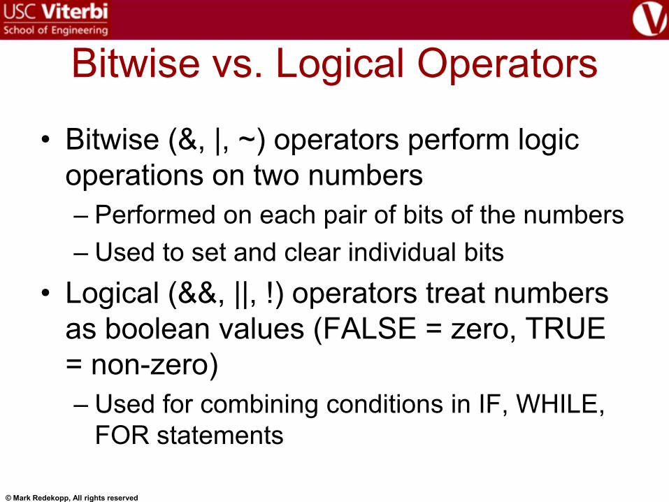
Bitwise vs. Logical Operators
• Bitwise (&, |, ~) operators perform logic
operations on two numbers
– Performed on each pair of bits of the numbers
– Used to set and clear individual bits
• Logical (&&, ||, !) operators treat numbers
as boolean values (FALSE = zero, TRUE
= non-zero)
– Used for combining conditions in IF, WHILE,
FOR statements

© Mark Redekopp, All rights reserved
Bitwise vs. Logical Operator Examples
a = 0xf0; b = 0x0f;
y = 0; z = 0;
if (a && b) y = 1;
if (a & b) z = 1;
Example 1
// enter IF statement if REG[0]=1
#define STAT_BIT0 0x01
if((REG & STAT_BIT0) == STAT_BIT0)
{ ... }
Example 2
// enter IF statement if REGA[7]=1 AND REGB[2]=0
if((REGA & 0x80) && !(REGB & 0x04))
{ ... }
Example 3
What will the final
values of y and z be?


