24
EE 4345 – Semiconductor Electronics Design Project – Spring 2002 Kevin Bradford Corey Clark Carlos Garcia Guillaume Gbetibouo Eric Goebel Fariba Pouya
EE 4345 – Semiconductor Electronics
Design Project – Spring 2002
Kevin Bradford
Corey Clark
Carlos Garcia
Guillaume Gbetibouo
Eric Goebel
Fariba Pouya
ANALOG BiCMOS
What is BiCMOS?
BiCMOS technology combinesBipolar and CMOS transistors onto asingle integrated circuit where theadvantages of both can be utilized.
• Power dissipation• Noise margin• Packing density• The ability to integrate large comples
functions with high yields
• Switching speed• Currents drive per unit area• Noise perfomance• Analog capability• Input/output speed
• Improved speed over CMOS• Lower power dissipation than Bipolar• Flexible input/outputs• High performance analog• Latch up immunity
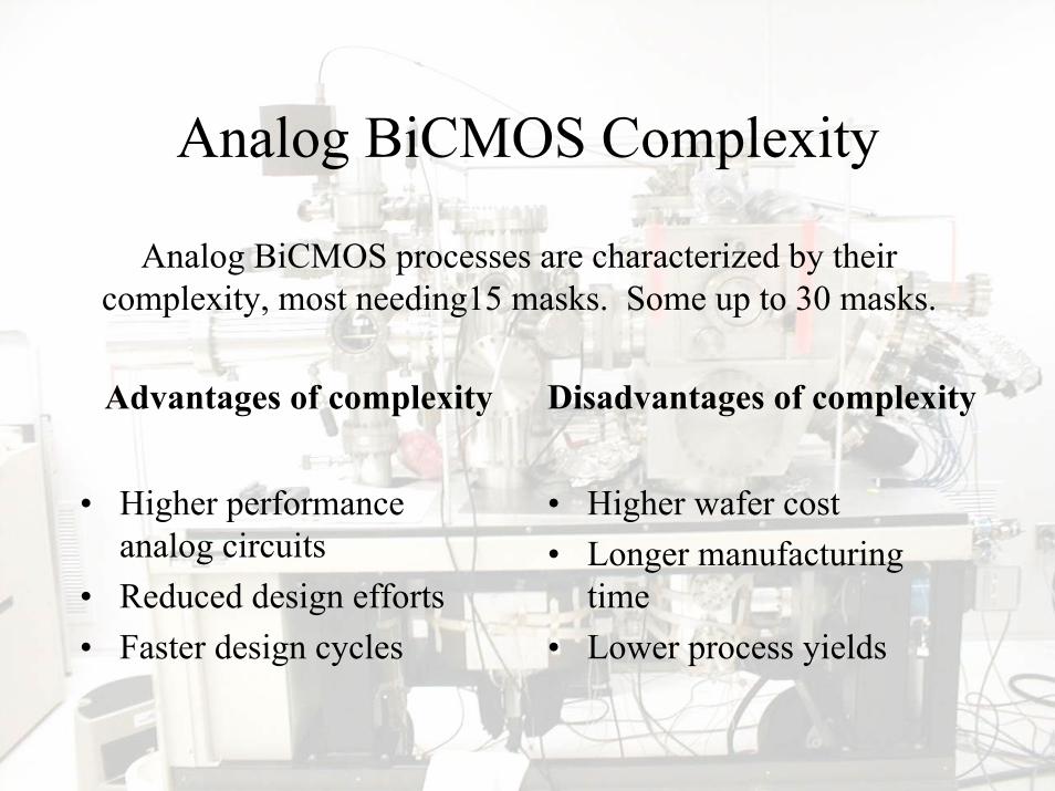
• Higher performanceanalog circuits
• Reduced design efforts• Faster design cycles
• Higher wafer cost• Longer manufacturing
time• Lower process yields
Analog BiCMOS processes are characterized by theircomplexity, most needing15 masks. Some up to 30 masks.
Advantages of complexity Disadvantages of complexity
BiCMOS technologies have tended to evolve from CMOSprocesses in order to obtain the highest CMOSperformance possible.
The bipolar processing steps have been added to the coreCMOS flow to realize the desired device characteristics.
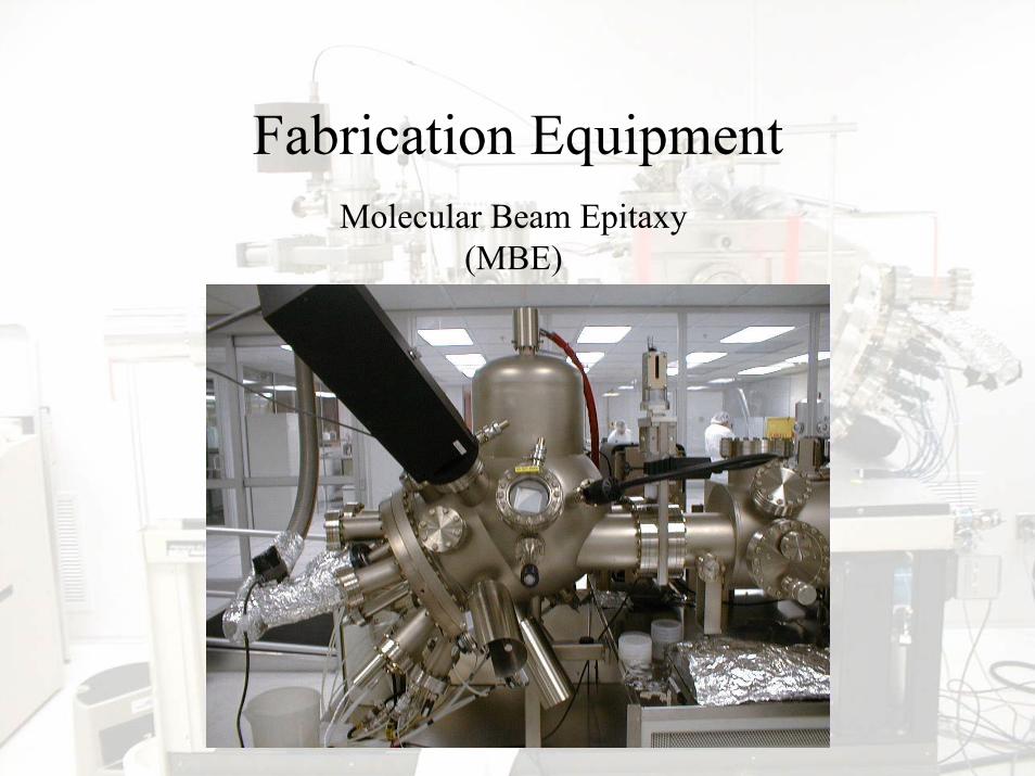
Molecular Beam Epitaxy(MBE)
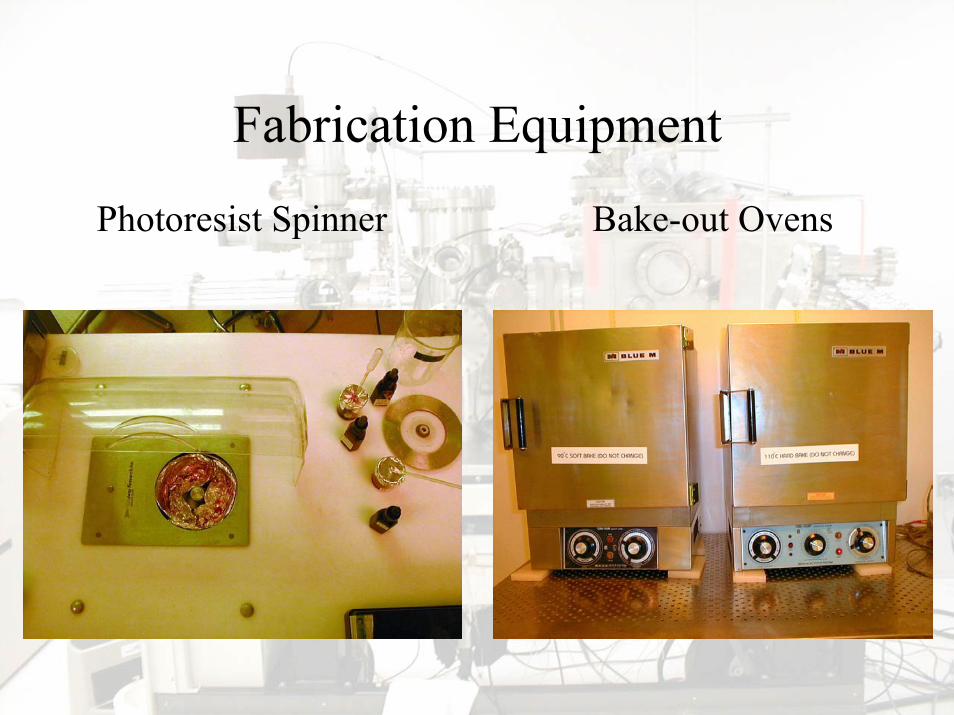
Photoresist Spinner Bake-out Ovens
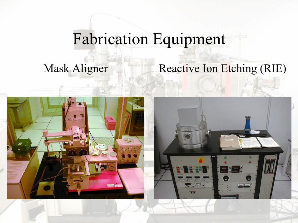
Mask Aligner Reactive Ion Etching (RIE)
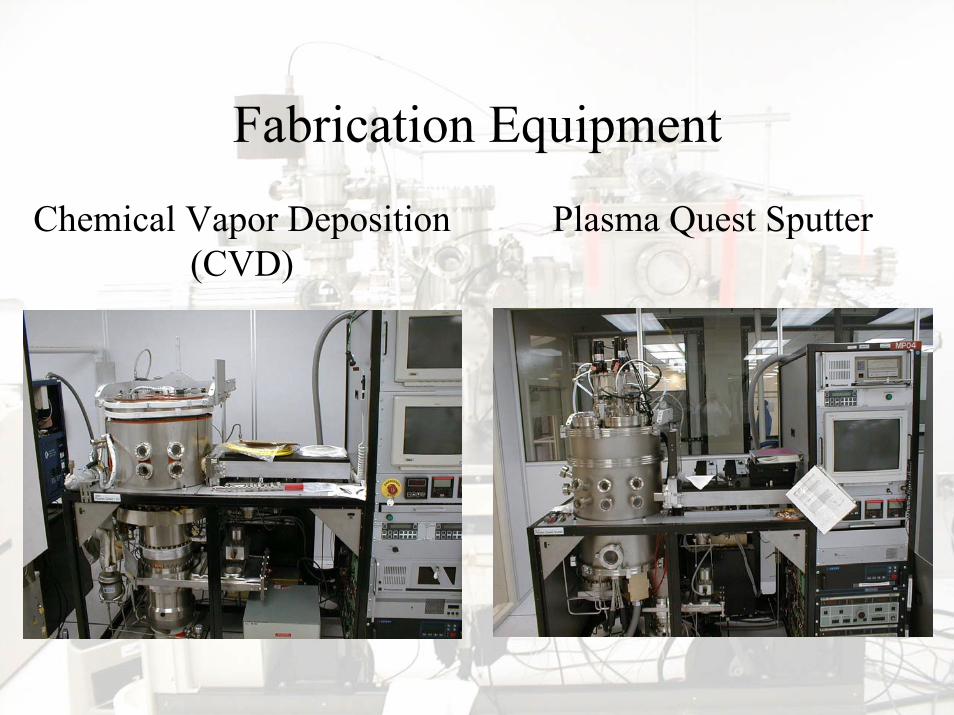
Chemical Vapor Deposition(CVD)
Plasma Quest Sputter
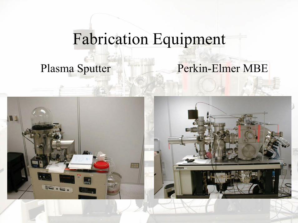
Plasma Sputter Perkin-Elmer MBE
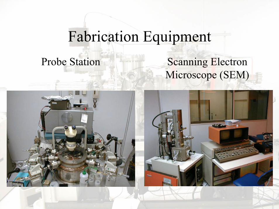
Probe Station Scanning ElectronMicroscope (SEM)
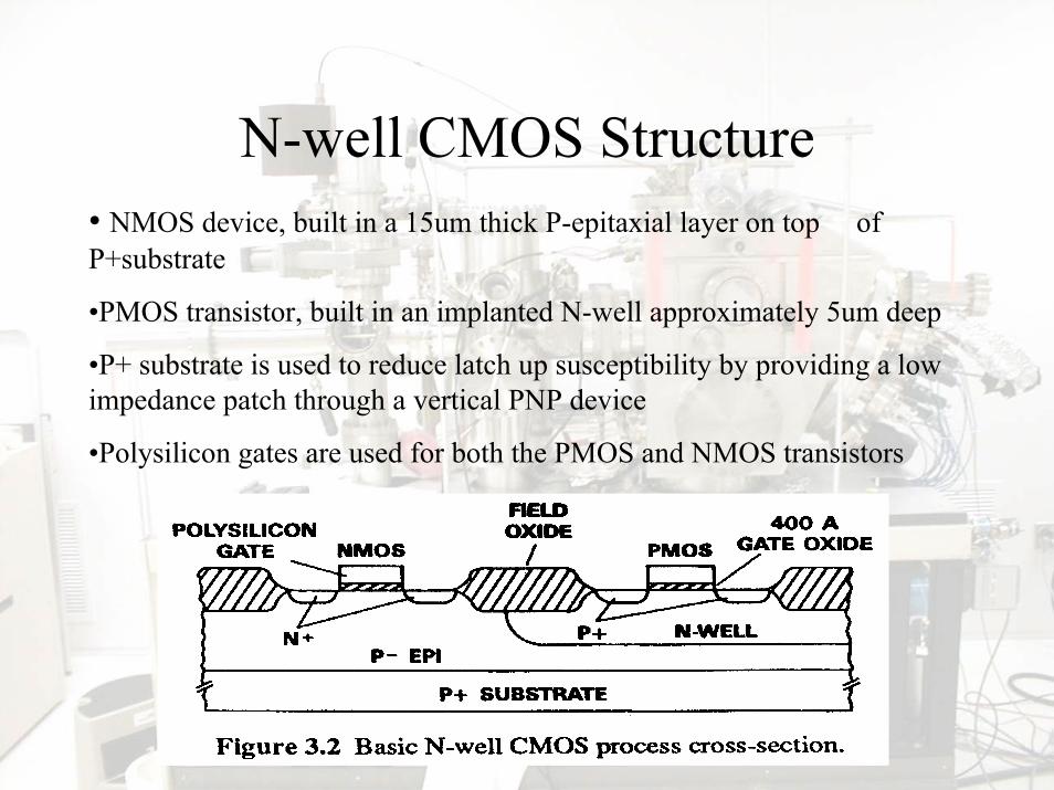
• NMOS device, built in a 15um thick P-epitaxial layer on top ofP+substrate
•PMOS transistor, built in an implanted N-well approximately 5um deep
•P+ substrate is used to reduce latch up susceptibility by providing a lowimpedance patch through a vertical PNP device
•Polysilicon gates are used for both the PMOS and NMOS transistors
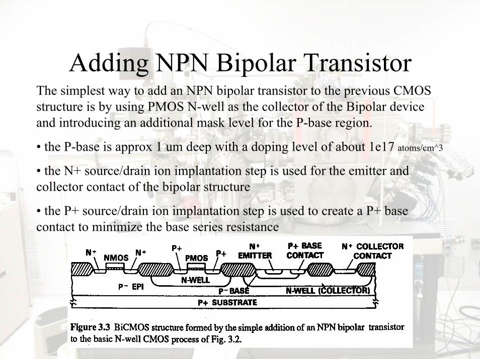
The simplest way to add an NPN bipolar transistor to the previous CMOSstructure is by using PMOS N-well as the collector of the Bipolar deviceand introducing an additional mask level for the P-base region.
• the P-base is approx 1 um deep with a doping level of about 1e17 atoms/cm^3
• the N+ source/drain ion implantation step is used for the emitter andcollector contact of the bipolar structure
• the P+ source/drain ion implantation step is used to create a P+ basecontact to minimize the base series resistance
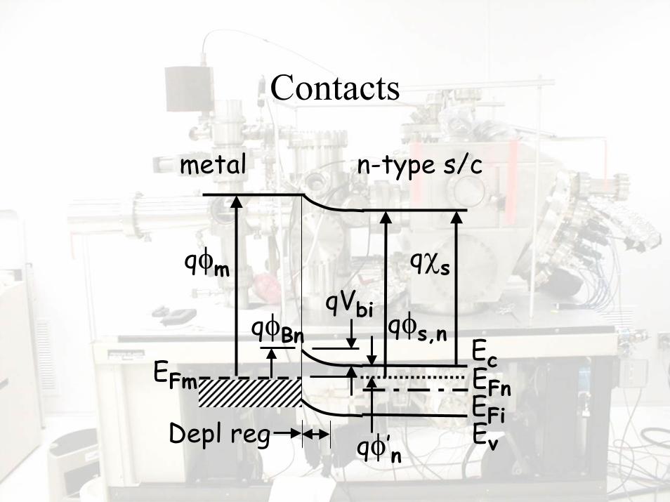
EFn
Ec
EvEFi
q�s,n
q�s
n-type s/c
q�m
EFm
metal
q�BnqVbi
q�’nDepl reg
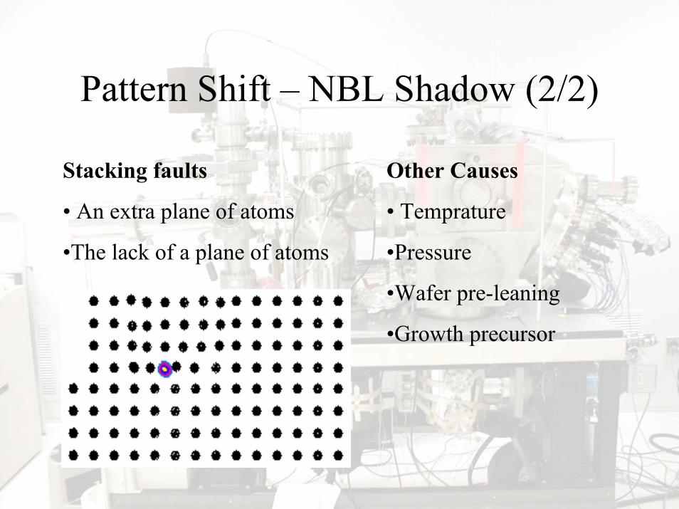
Stacking faults
• An extra plane of atoms
•The lack of a plane of atoms
Other Causes
• Temprature
•Pressure
•Wafer pre-leaning
•Growth precursor
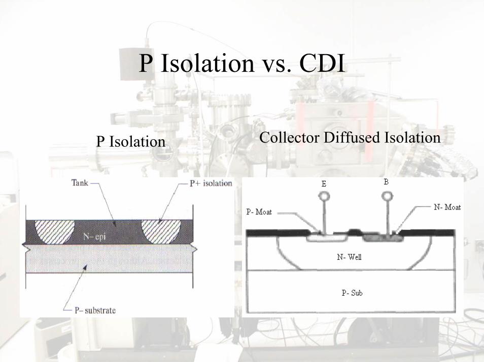
Collector Diffused IsolationP Isolation
• Key factor in determining overall circuit performance anddensity
• Collector Diffused Isolation (CDI)– N-well used to form collector of NPN transistor– Base and emitter consist of successive counterdoping of
the well.– CDI transistors
• Saturate prematurely• Limits low-voltage operation• Complicates device modeling• Causes undesired substrate injection
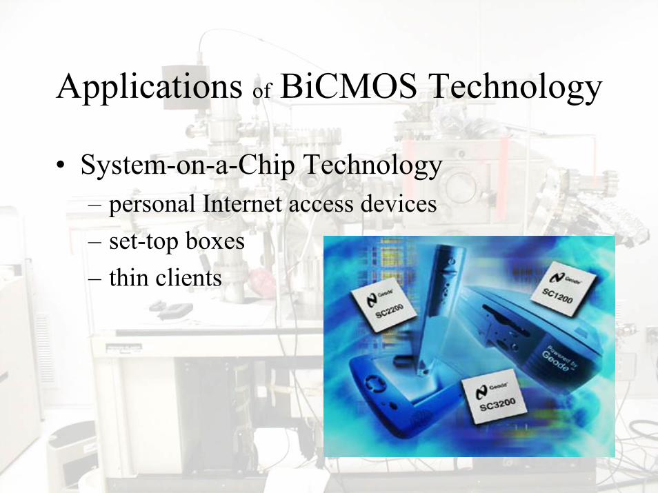
• System-on-a-Chip Technology– personal Internet access devices– set-top boxes– thin clients
of
• Carter, Ronald. “Lecture 9 – EE 5342” UTA • Cheung, Nathan “ Lecture 17 – EE 143” UC Berkeley • http: //et.nmso.edu/ETCLASSES/vlsi/files/CRYSTAL.HTM • Hastings, Alan “The Art of Analog Layout”, Prentice Hall, New Jersey,
2001 • Campbell, Stephen A. , “The Science and Engineering of
Microelectronic Fabrication”, Oxford University Press, New York,2001
• Alvarez, Antonio, “BiCMOS Technology and Applications”, PrenticeHall, New Jersey, 2001


