35
EE 5340 Semiconductor Device Theory Lecture 4 - Fall 2009 Professor Ronald L. Carter [email protected] http://www.uta.edu/ronc
| Date post: | 31-Dec-2015 |
| Category: |
Documents |
| Upload: | marcia-barker |
| View: | 46 times |
| Download: | 2 times |
EE 5340Semiconductor Device TheoryLecture 4 - Fall 2009
Professor Ronald L. [email protected]
http://www.uta.edu/ronc

L 04 Sept 04
First Assignment
• Send e-mail to [email protected]– On the subject line, put “5340 e-mail”– In the body of message include
• email address: ______________________• Your Name*: _______________________• Last four digits of your Student ID: _____
* Your name as it appears in the UTA Record - no more, no less
2

L 04 Sept 04
Second Assignment
• Please print and bring to class a signed copy of the document appearing at
http://www.uta.edu/ee/COE%20Ethics%20Statement%20Fall%2007.pdf
3
L 04 Sept 04
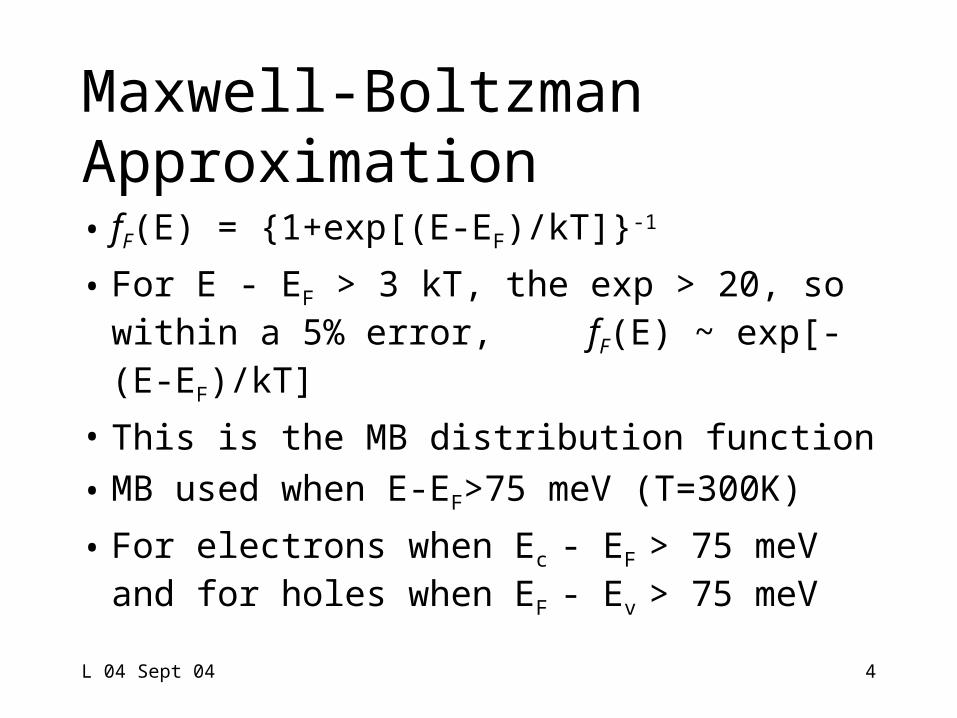
Maxwell-BoltzmanApproximation• fF(E) = {1+exp[(E-EF)/kT]}-1
• For E - EF > 3 kT, the exp > 20, so within a 5% error, fF(E) ~ exp[-(E-EF)/kT]
• This is the MB distribution function
• MB used when E-EF>75 meV (T=300K)
• For electrons when Ec - EF > 75 meV and for holes when EF - Ev > 75 meV
4
L 04 Sept 04
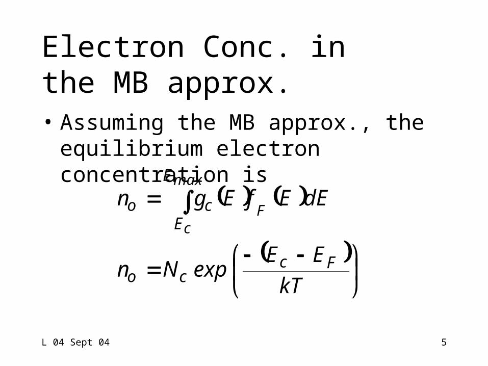
Electron Conc. inthe MB approx.• Assuming the MB approx., the
equilibrium electron concentration is
kTEE
expNn
dEEfEgn
Fcco
E
Eco F
max
c
5
L 04 Sept 04
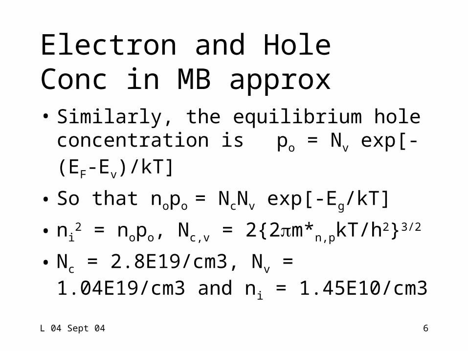
Electron and HoleConc in MB approx• Similarly, the equilibrium hole
concentration ispo = Nv exp[-(EF-Ev)/kT]
• So that nopo = NcNv exp[-Eg/kT]
• ni2 = nopo, Nc,v = 2{2m*n,pkT/h2}3/2
• Nc = 2.8E19/cm3, Nv = 1.04E19/cm3 and ni = 1.45E10/cm3
6
L 04 Sept 04
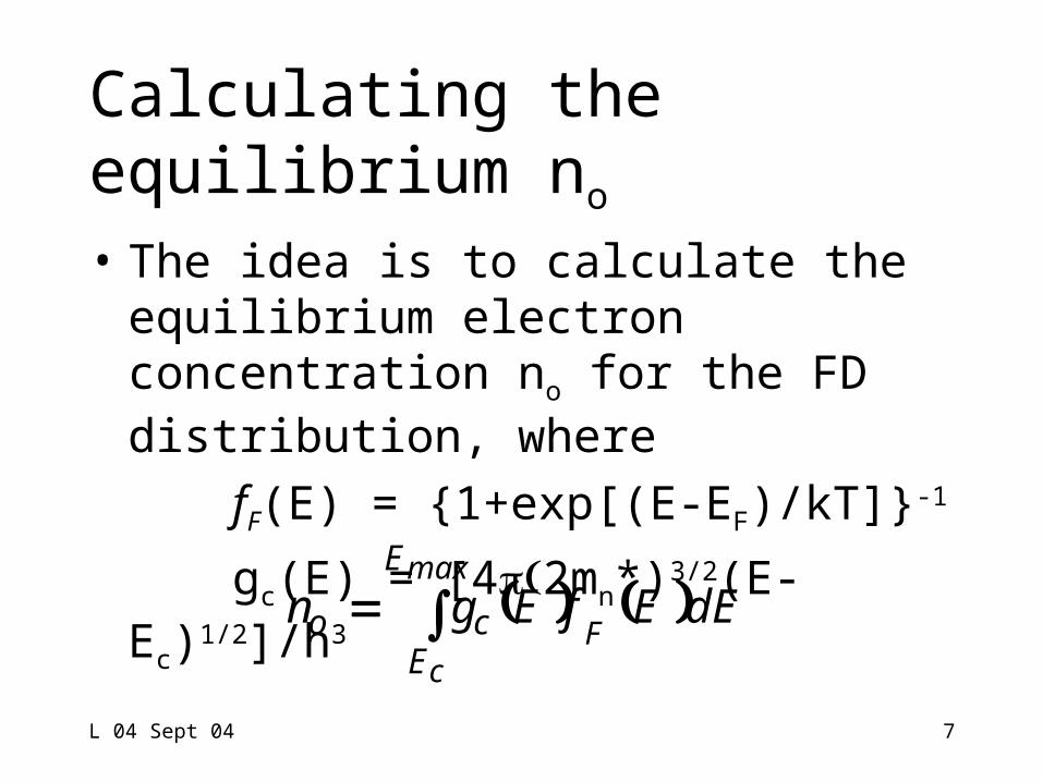
Calculating theequilibrium no
• The idea is to calculate the equilibrium electron concentration no for the FD distribution, where
fF(E) = {1+exp[(E-EF)/kT]}-1
gc(E) = [42mn*)3/2(E-Ec)1/2]/h3
dEEfEgnF
max
c
E
Eco
7
L 04 Sept 04
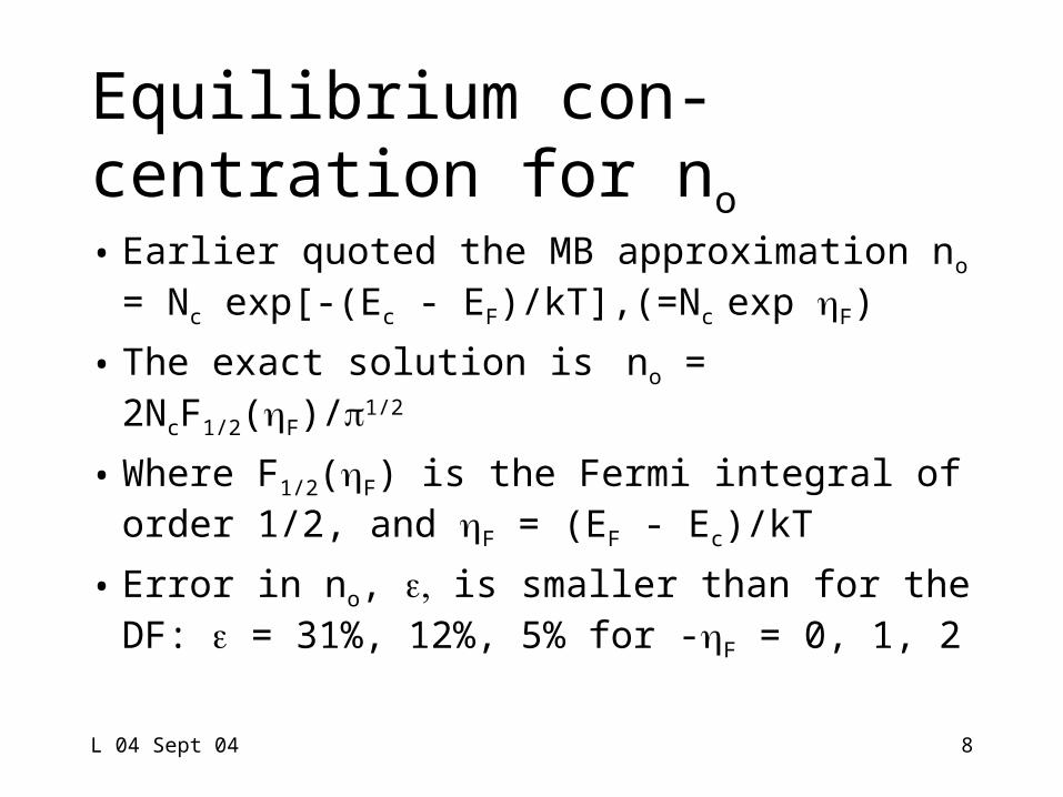
Equilibrium con-centration for no
• Earlier quoted the MB approximation no = Nc exp[-(Ec - EF)/kT],(=Nc exp F)
• The exact solution is no = 2NcF1/2(F)/1/2
• Where F1/2(F) is the Fermi integral of order 1/2, and F = (EF - Ec)/kT
• Error in no, is smaller than for the DF: = 31%, 12%, 5% for -F = 0, 1, 2
8
L 04 Sept 04
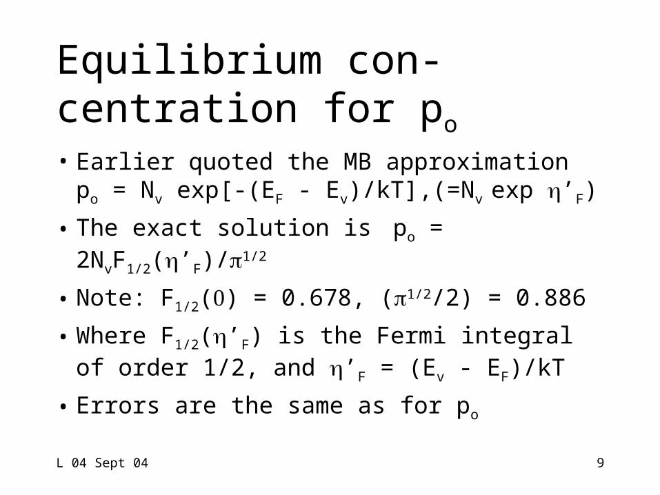
Equilibrium con-centration for po
• Earlier quoted the MB approximation po = Nv exp[-(EF - Ev)/kT],(=Nv exp ’F)
• The exact solution is po = 2NvF1/2(’F)/1/2
• Note: F1/2() = 0.678, (1/2/2) = 0.886
• Where F1/2(’F) is the Fermi integral of order 1/2, and ’F = (Ev - EF)/kT
• Errors are the same as for po
9
L 04 Sept 04
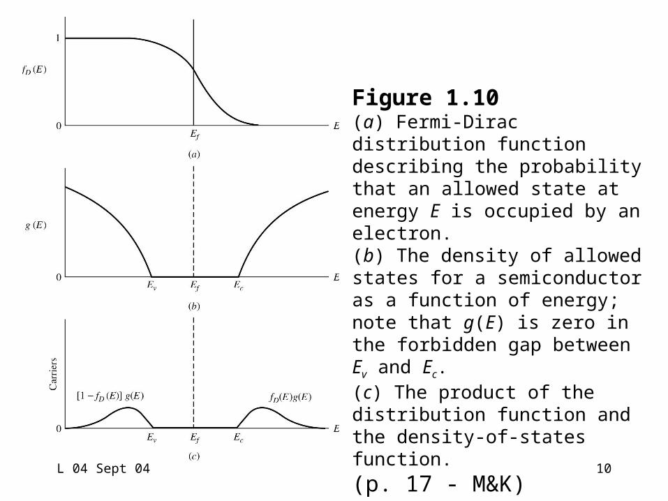
Figure 1.10 (a) Fermi-Dirac distribution function describing the probability that an allowed state at energy E is occupied by an electron. (b) The density of allowed states for a semiconductor as a function of energy; note that g(E) is zero in the forbidden gap between Ev and Ec.(c) The product of the distribution function and the density-of-states function. (p. 17 - M&K)
10
L 04 Sept 04
Degenerate andnondegenerate cases• Bohr-like doping model assumes no
interaction between dopant sites• If adjacent dopant atoms are within 2
Bohr radii, then orbits overlap
• This happens when Nd ~ Nc (EF ~ Ec), or when Na ~ Nv (EF ~ Ev)
• The degenerate semiconductor is defined by EF ~/> Ec or EF ~/< Ev
11
L 04 Sept 04
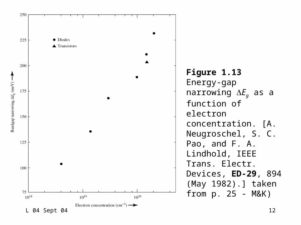
Figure 1.13 Energy-gap narrowing Eg as a function of electron concentration. [A. Neugroschel, S. C. Pao, and F. A. Lindhold, IEEE Trans. Electr. Devices, ED-29, 894 (May 1982).] taken from p. 25 - M&K)
12
L 04 Sept 04
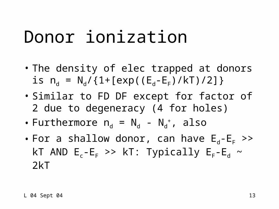
Donor ionization
• The density of elec trapped at donors is nd = Nd/{1+[exp((Ed-EF)/kT)/2]}
• Similar to FD DF except for factor of 2 due to degeneracy (4 for holes)
• Furthermore nd = Nd - Nd+, also
• For a shallow donor, can have Ed-EF >> kT AND Ec-EF >> kT: Typically EF-Ed ~ 2kT
13
L 04 Sept 04
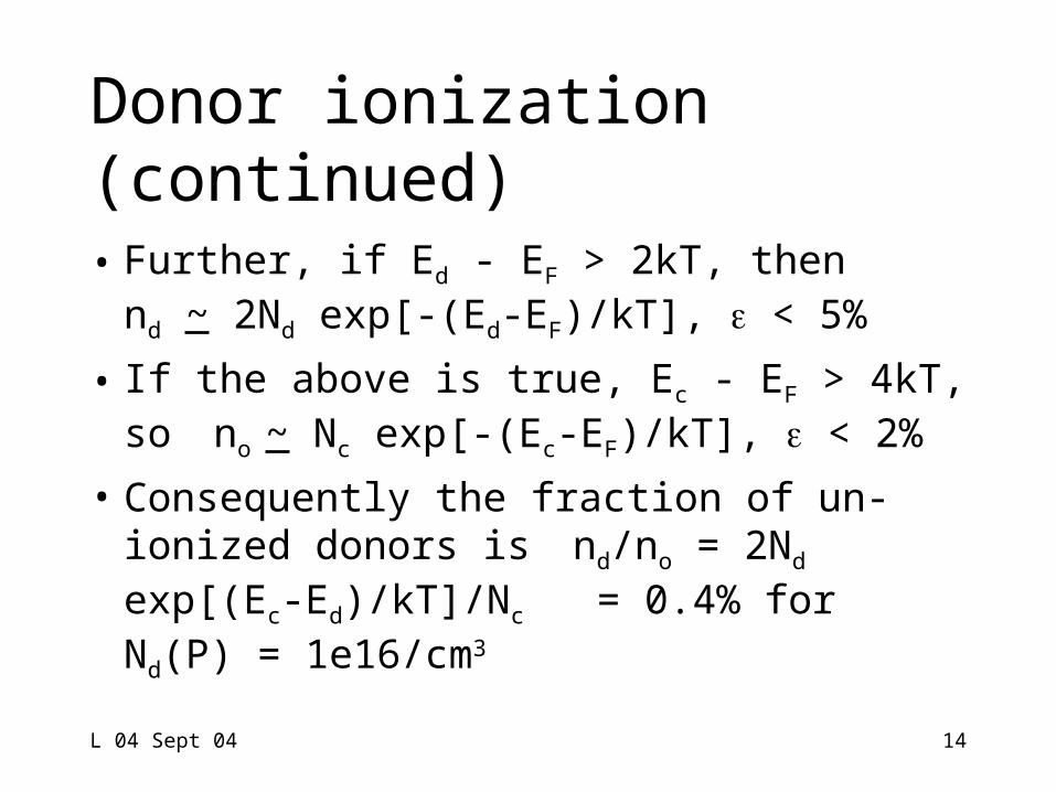
Donor ionization(continued)• Further, if Ed - EF > 2kT, then
nd ~ 2Nd exp[-(Ed-EF)/kT], < 5%
• If the above is true, Ec - EF > 4kT, sono ~ Nc exp[-(Ec-EF)/kT], < 2%
• Consequently the fraction of un-ionized donors is nd/no = 2Nd exp[(Ec-Ed)/kT]/Nc = 0.4% for Nd(P) = 1e16/cm3
14
L 04 Sept 04
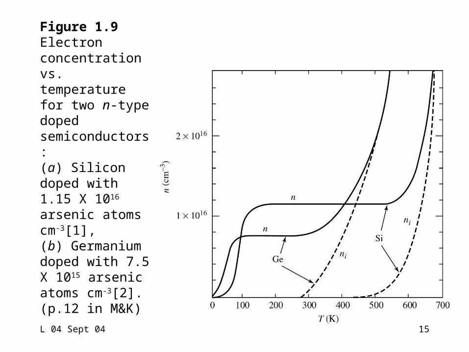
Figure 1.9 Electron concentration vs. temperature for two n-type doped semiconductors:(a) Silicon doped with 1.15 X 10¹⁶ arsenic atoms cm-3[1], (b) Germanium doped with 7.5 X 10¹⁵ arsenic atoms cm-3[2]. (p.12 in M&K)
15
L 04 Sept 04
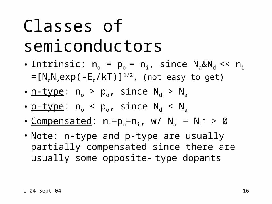
Classes ofsemiconductors• Intrinsic: no = po = ni, since Na&Nd << ni
=[NcNvexp(-Eg/kT)]1/2, (not easy to get)
• n-type: no > po, since Nd > Na
• p-type: no < po, since Nd < Na
• Compensated: no=po=ni, w/ Na- = Nd
+ > 0
• Note: n-type and p-type are usually partially compensated since there are usually some opposite- type dopants
16
L 04 Sept 04
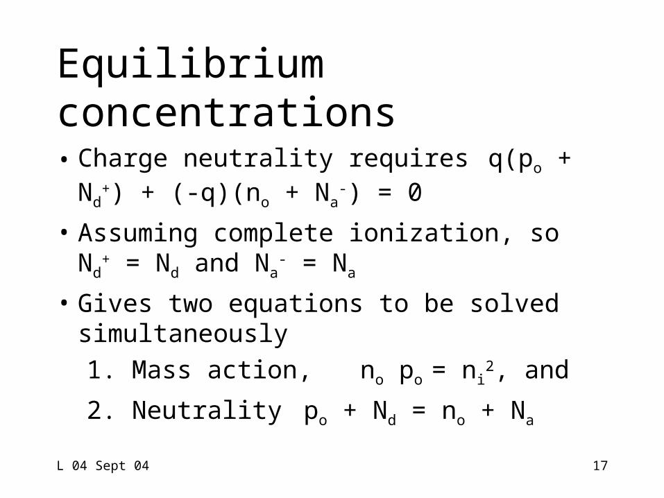
Equilibriumconcentrations• Charge neutrality requires
q(po + Nd+) + (-q)(no + Na
-) = 0
• Assuming complete ionization, so Nd
+ = Nd and Na- = Na
• Gives two equations to be solved simultaneously
1. Mass action, no po = ni2, and
2. Neutrality po + Nd = no + Na
17
L 04 Sept 04 18
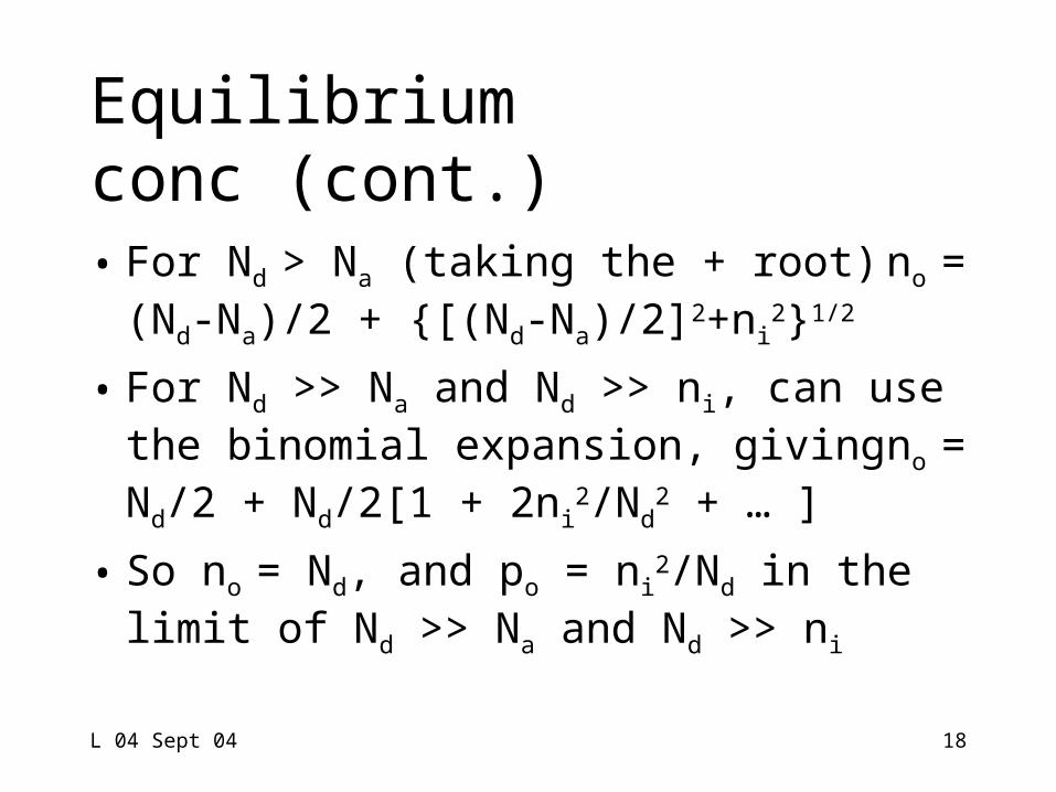
Equilibriumconc (cont.)• For Nd > Na (taking the + root) no
= (Nd-Na)/2 + {[(Nd-Na)/2]2+ni2}1/2
• For Nd >> Na and Nd >> ni, can use the binomial expansion, giving
no = Nd/2 + Nd/2[1 + 2ni2/Nd
2 + … ]
• So no = Nd, and po = ni2/Nd in the limit
of Nd >> Na and Nd >> ni

L 04 Sept 04 19
Examplecalculations• For Nd = 3.2E16/cm3, ni = 1.4E10/cm3
no = Nd = 3.2E16/cm3
po = ni2/Nd , (po is always ni
2/no)
= (1.4E10/cm3)2/3.2E16/cm3
= 6.125E3/cm3 (comp to ~1E23 Si)
• For po = Na = 4E17/cm3,
no = ni2/Na = (1.4E10/cm3)2/4E17/cm3
= 490/cm3
L 04 Sept 04 20
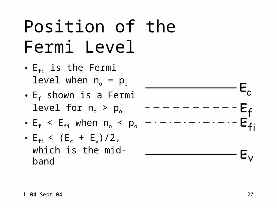
Position of theFermi Level• Efi is the Fermi level
when no = po
• Ef shown is a Fermi level for no > po
• Ef < Efi when no < po
• Efi < (Ec + Ev)/2, which is the mid-band
L 04 Sept 04 21
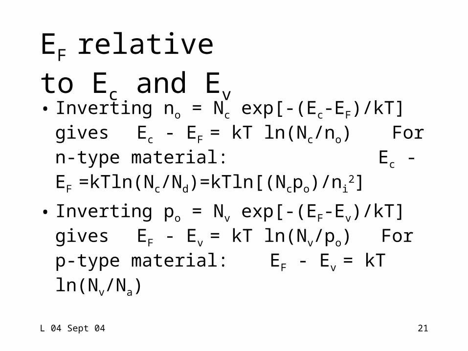
EF relative to Ec and Ev• Inverting no = Nc exp[-(Ec-EF)/kT] gives
Ec - EF = kT ln(Nc/no) For n-type material: Ec - EF
=kTln(Nc/Nd)=kTln[(Ncpo)/ni2]
• Inverting po = Nv exp[-(EF-Ev)/kT] gives EF - Ev = kT ln(Nv/po) For p-type material: EF - Ev = kT ln(Nv/Na)
L 04 Sept 04 22
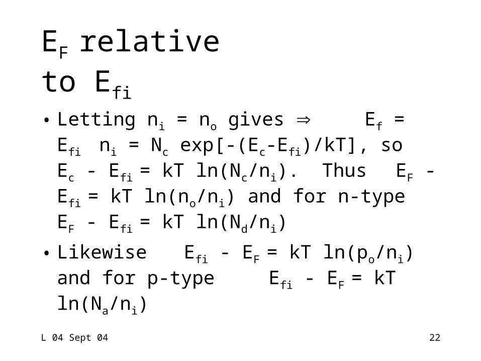
EF relative to Efi
• Letting ni = no gives Ef = Efi ni = Nc exp[-(Ec-Efi)/kT], so Ec - Efi = kT ln(Nc/ni). Thus EF - Efi = kT ln(no/ni) and for n-type EF - Efi = kT ln(Nd/ni)
• Likewise Efi - EF = kT ln(po/ni) and for p-type Efi - EF = kT ln(Na/ni)
L 04 Sept 04 23
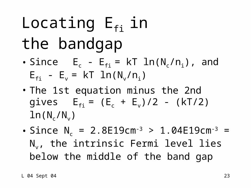
Locating Efi in the bandgap • Since
Ec - Efi = kT ln(Nc/ni), andEfi - Ev = kT ln(Nv/ni)
• The 1st equation minus the 2nd givesEfi = (Ec + Ev)/2 - (kT/2) ln(Nc/Nv)
• Since Nc = 2.8E19cm-3 > 1.04E19cm-3 = Nv, the intrinsic Fermi level lies below the middle of the band gap
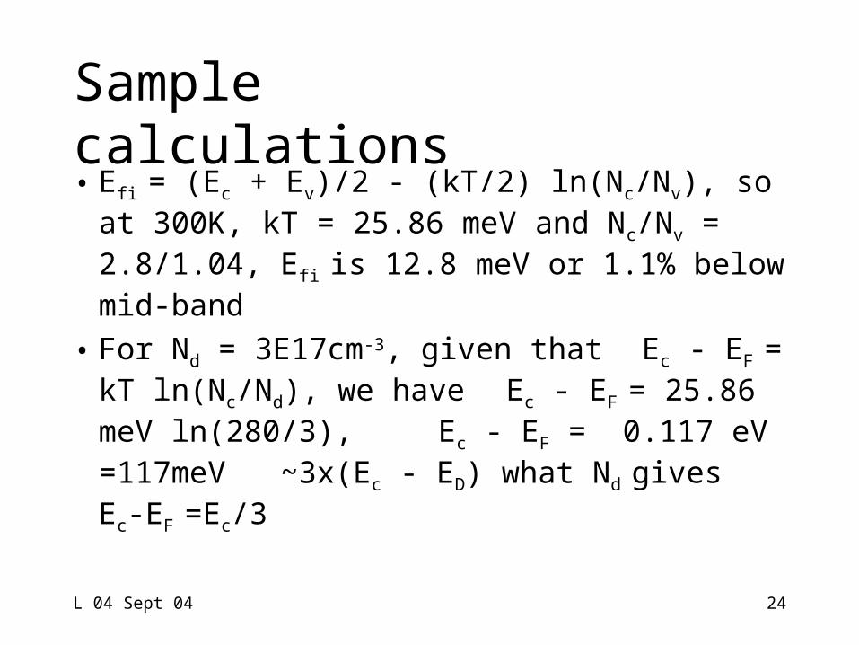
L 04 Sept 04 24
Samplecalculations• Efi = (Ec + Ev)/2 - (kT/2) ln(Nc/Nv), so at
300K, kT = 25.86 meV and Nc/Nv = 2.8/1.04, Efi is 12.8 meV or 1.1% below mid-band
• For Nd = 3E17cm-3, given that Ec - EF = kT ln(Nc/Nd), we have Ec - EF
= 25.86 meV ln(280/3), Ec - EF = 0.117 eV =117meV ~3x(Ec - ED) what Nd
gives Ec-EF =Ec/3
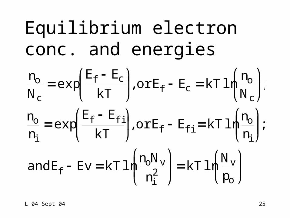
L 04 Sept 04 25
Equilibrium electronconc. and energies
o
v2i
vof
i
ofif
fif
i
o
c
ocf
cf
c
o
pN
lnkTn
NnlnkTEvE and
;nn
lnkTEE or ,kT
EEexp
nn
;Nn
lnkTEE or ,kT
EEexp
Nn
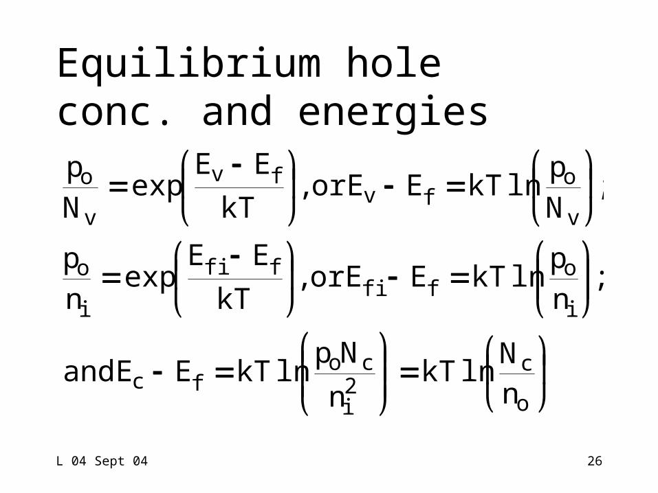
L 04 Sept 04 26
Equilibrium hole conc. and energies
o
c2i
cofc
i
offi
ffi
i
o
v
ofv
fv
v
o
nN
lnkTn
NplnkTEE and
;np
lnkTEE or ,kT
EEexp
np
;Np
lnkTEE or ,kT
EEexp
Np
L 04 Sept 04 27
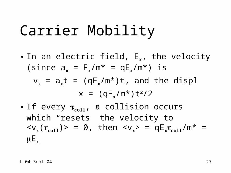
Carrier Mobility
• In an electric field, Ex, the velocity (since ax = Fx/m* = qEx/m*) is
vx = axt = (qEx/m*)t, and the displ
x = (qEx/m*)t2/2
• If every coll, a collision occurs which “resets” the velocity to <vx(coll)> = 0, then <vx> = qExcoll/m* = Ex
L 04 Sept 04 28
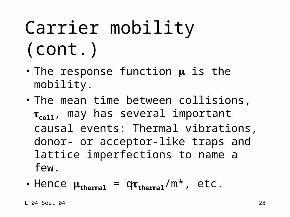
Carrier mobility (cont.)• The response function is the
mobility.• The mean time between collisions,
coll, may has several important causal events: Thermal vibrations, donor- or acceptor-like traps and lattice imperfections to name a few.
• Hence thermal = qthermal/m*, etc.
L 04 Sept 04 29
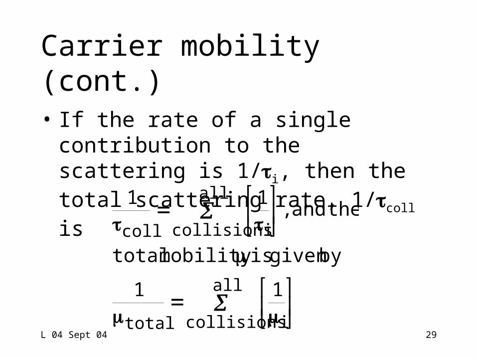
Carrier mobility (cont.)• If the rate of a single contribution
to the scattering is 1/i, then the total scattering rate, 1/coll is
all
collisions itotal
all
collisions icoll
11
by given is mobility total
the and , 11
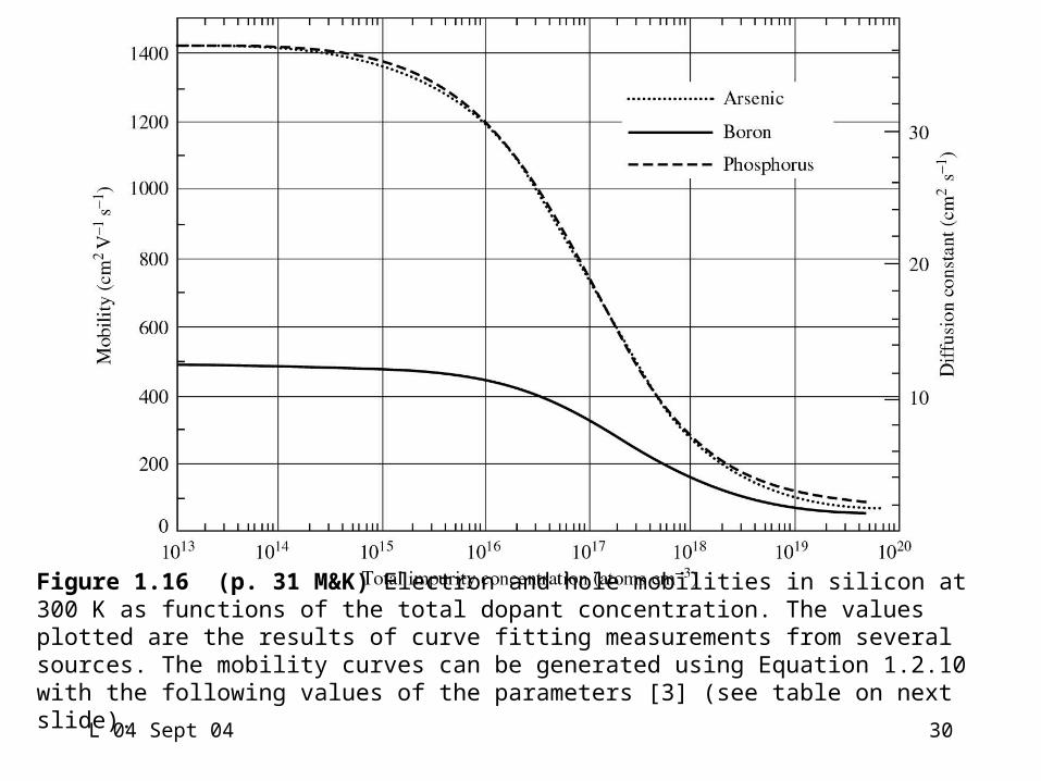
Figure 1.16 (p. 31 M&K) Electron and hole mobilities in silicon at 300 K as functions of the total dopant concentration. The values plotted are the results of curve fitting measurements from several sources. The mobility curves can be generated using Equation 1.2.10 with the following values of the parameters [3] (see table on next slide).
L 04 Sept 04 30
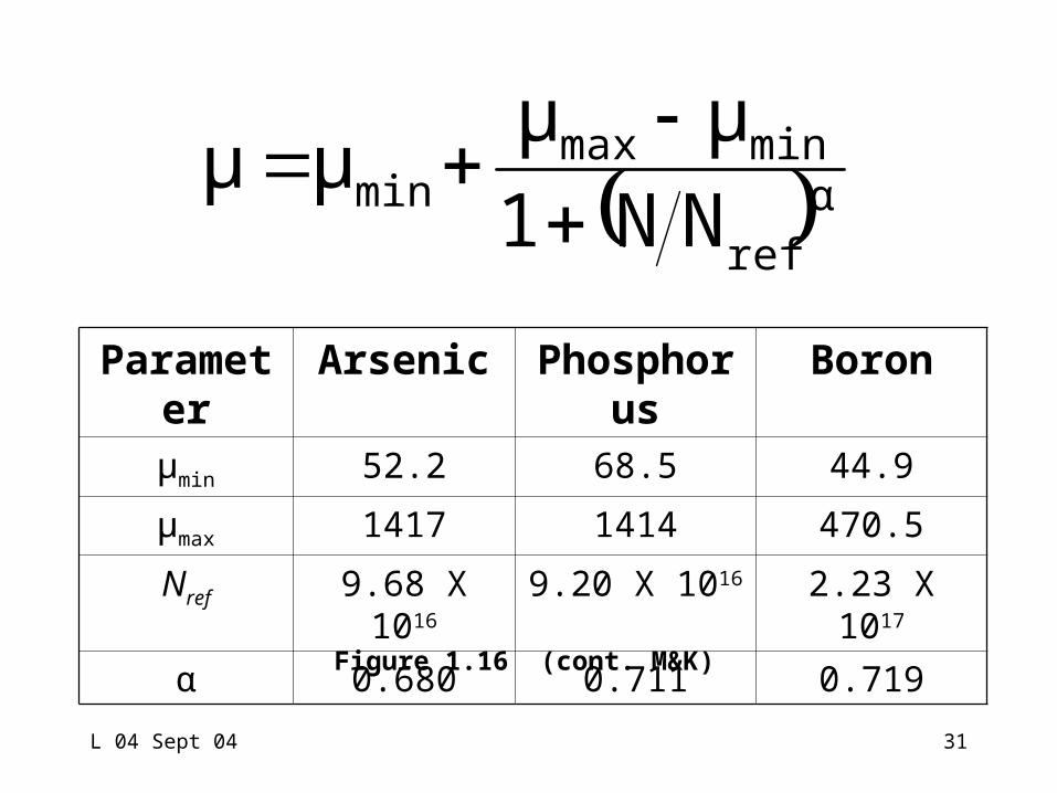
Figure 1.16 (cont. M&K)
Parameter Arsenic Phosphorus Boronμmin 52.2 68.5 44.9
μmax 1417 1414 470.5
Nref 9.68 X 10¹⁶ 9.20 X 10¹⁶ 2.23 X 10¹⁷
α 0.680 0.711 0.719
L 04 Sept 04 31
αμμ
μμref
minmaxmin NN1
L 04 Sept 04 32
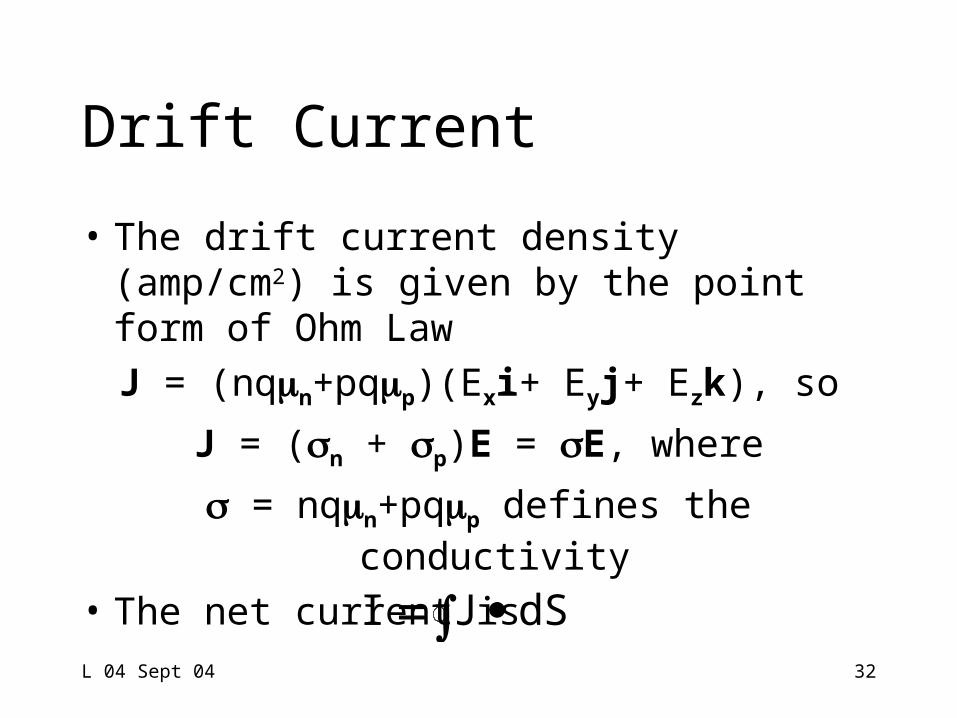
Drift Current
• The drift current density (amp/cm2) is given by the point form of Ohm LawJ = (nqn+pqp)(Exi+ Eyj+ Ezk), so
J = (n + p)E = E, where
= nqn+pqp defines the conductivity
• The net current is SdJI
L 04 Sept 04 33
Net silicon extrresistivity (cont.)• Since = (nqn + pqp)-1, and
n > p, ( = q/m*) we have
p > n
• Note that since1.6(high conc.) < p/n < 3(low conc.), so
1.6(high conc.) < n/p < 3(low conc.)
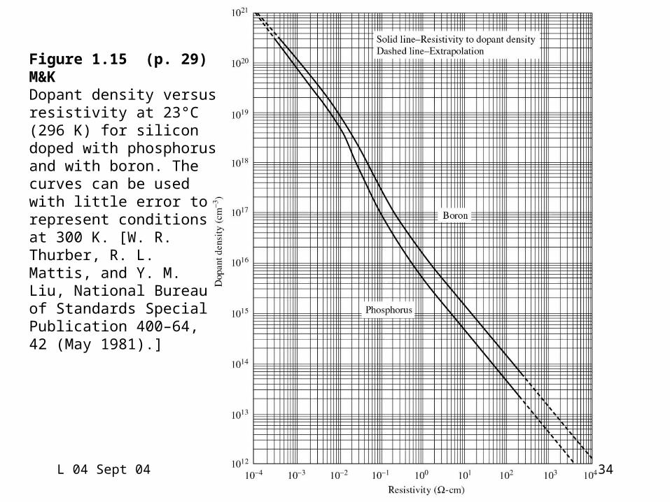
Figure 1.15 (p. 29) M&K Dopant density versus resistivity at 23°C (296 K) for silicon doped with phosphorus and with boron. The curves can be used with little error to represent conditions at 300 K. [W. R. Thurber, R. L. Mattis, and Y. M. Liu, National Bureau of Standards Special Publication 400–64, 42 (May 1981).]
L 04 Sept 04 34
L 04 Sept 04
References
*Fundamentals of Semiconductor Theory and Device Physics, by Shyh Wang, Prentice Hall, 1989.
**Semiconductor Physics & Devices, by Donald A. Neamen, 2nd ed., Irwin, Chicago.
M&K = Device Electronics for Integrated Circuits, 3rd ed., by Richard S. Muller, Theodore I. Kamins, and Mansun Chan, John Wiley and Sons, New York, 2003.
35


