EE3101 LAB REPORT EXP#6 06 DEC 2006 _______________________________________________________________________ High-frequency Behavior of Bi-Polar Junction Transistors Matt xxxxx Student ID : xxxxxxx 10/2/06 – 10/16/06 Abstract In this experiment we will measure the input and output of various BJT- based amplifiers to determine the value of the BJT’s internal components, such as and which are included in the -1-
High-frequency Behavior of Bi-Polar Junction Transistors
Matt xxxxx Student ID : xxxxxxx
10/2/06 – 10/16/06
Abstract
In this experiment we will measure the input and output of various BJT-based amplifiers to determine the value of the BJT’s internal components, such as and which are included in the hybrid-π small signal model. We will also investigate the effects of different amplifier designs on the midband gain and bandwidth of the circuit. We will show that the product of gain and bandwidth of amplifier designs is a constant value. This experiment is important because we will learn about the internal components of the BJT and the different designs of amplifiers that utilize the BJT.
IntroductionIn previous experiments, we looked at how the BJT can be used in amplification and current
mirroring applications; these were for medium to low frequency situations where the high frequency effects of the BJT were not eminent.
The focus of this experiment is the analysis of BJT-based amplifiers, and how the hybrid –π model describes the BJT in these situations. This model is well suited for small signal analysis and accounts for the internal capacitances of the BJT at high frequencies. During transistor operation, electric fields build up within the BJT and create intrinsic capacitances; we can see these capacitances represented as capacitors in our hybrid- π model
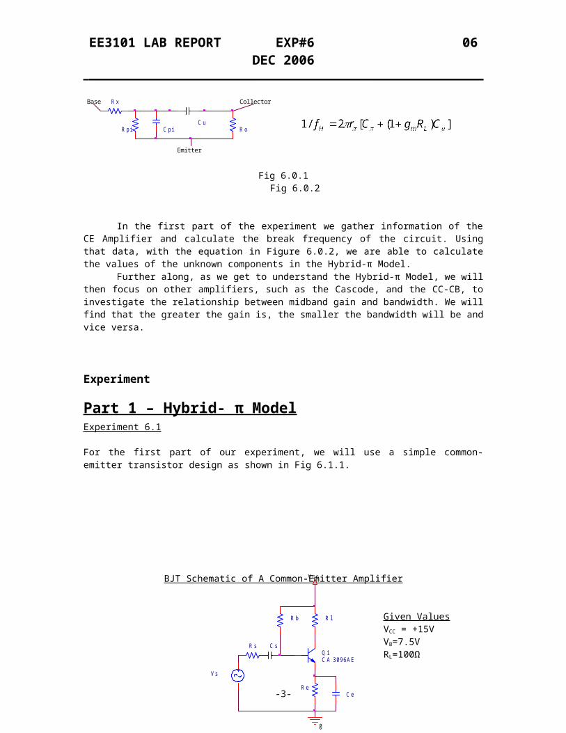
In this experiment we measure and calculate the components of the hybrid-π model (Figure 6.0.1) of the BJT which is commonly used to analyze the response of small signal inputs of a circuit at various frequencies, especially at high frequencies. The capacitance effect in the BJT does not show much effect at low frequencies, because they work as an open circuit. However, as the frequency may increase these capacitances work as a low-pass filter, which results in a decrease of the current or voltage gain. The break frequency, same as cutoff frequency, is calculated at the -3dB value of the max gain, which is the value of
. The relationship between the cutoff frequency and the components of the Hybrid-π Model is
given in Figure 6.0.2
R x
C p i
CollectorBase
R o
Emitter
C uR p i
Fig 6.0.1 Fig 6.0.2
In the first part of the experiment we gather information of the CE Amplifier and calculate the break frequency of the circuit. Using that data, with the equation in Figure 6.0.2, we are able to calculate the values of the unknown components in the Hybrid-π Model.
Further along, as we get to understand the Hybrid-π Model, we will then focus on other amplifiers, such as the Cascode, and the CC-CB, to investigate the relationship between midband gain and bandwidth. We will find that the greater the gain is, the smaller the bandwidth will be and vice versa.
Experiment
Part 1 – Hybrid- π ModelExperiment 6.1
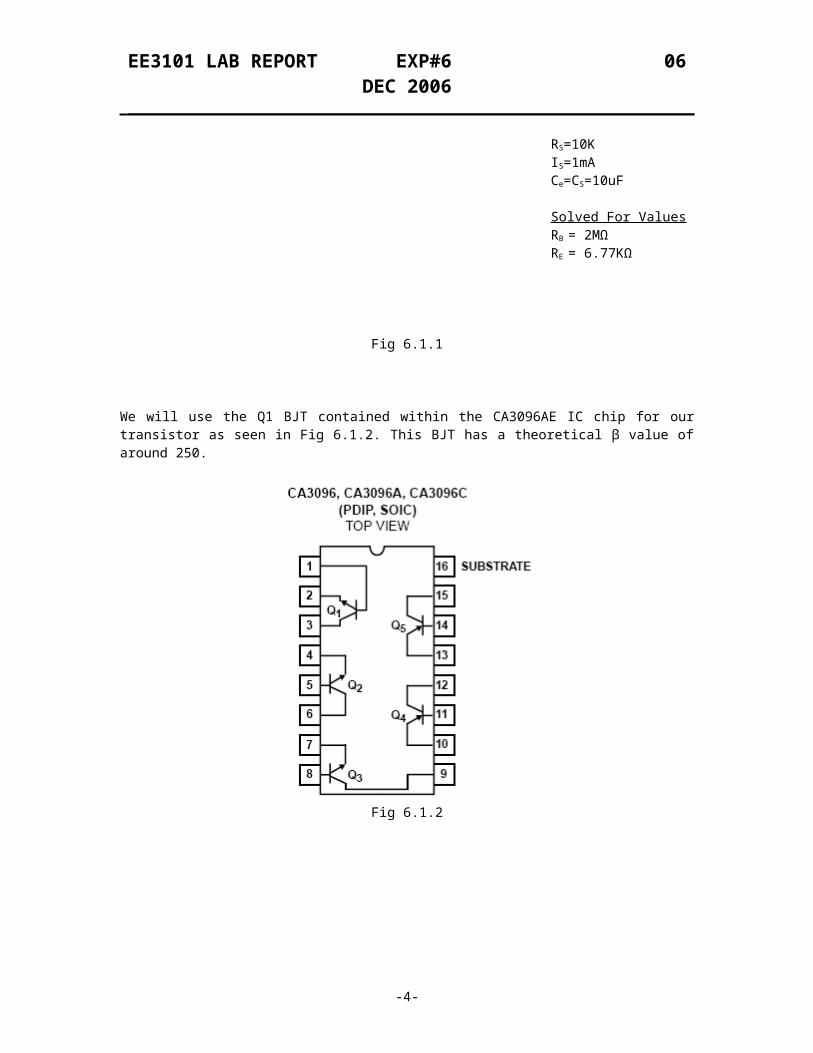
For the first part of our experiment, we will use a simple common-emitter transistor design as shown in Fig 6.1.1.
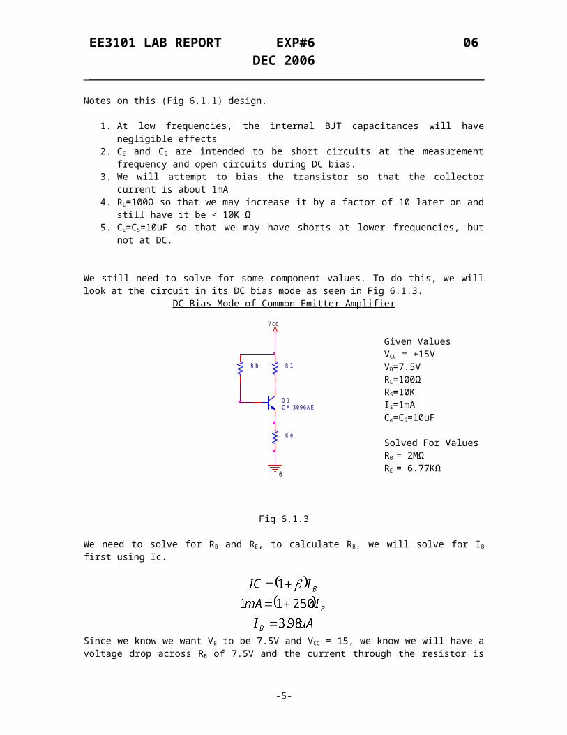
Given ValuesVCC = +15VVB=7.5VRL=100ΩRS=10KIS=1mACe=CS=10uF
Solved For ValuesRB = 2MΩRE = 6.77KΩ
Fig 6.1.1
We will use the Q1 BJT contained within the CA3096AE IC chip for our transistor as seen in Fig 6.1.2. This BJT has a theoretical β value of around 250.
1. At low frequencies, the internal BJT capacitances will have negligible effects2. CE and CS are intended to be short circuits at the measurement frequency and open circuits during
DC bias.3. We will attempt to bias the transistor so that the collector current is about 1mA4. RL=100Ω so that we may increase it by a factor of 10 later on and still have it be < 10K Ω5. CE=CS=10uF so that we may have shorts at lower frequencies, but not at DC.
We still need to solve for some component values. To do this, we will look at the circuit in its DC bias mode as seen in Fig 6.1.3.
DC Bias Mode of Common Emitter Amplifier
Given ValuesVCC = +15VVB=7.5VRL=100ΩRS=10KIS=1mACe=CS=10uF
Solved For ValuesRB = 2MΩRE = 6.77KΩ
Fig 6.1.3
We need to solve for RB and RE, to calculate RB, we will solve for IB first using Ic.
Since we know we want VB to be 7.5V and VCC = 15, we know we will have a voltage drop across RB of 7.5V and the current through the resistor is .
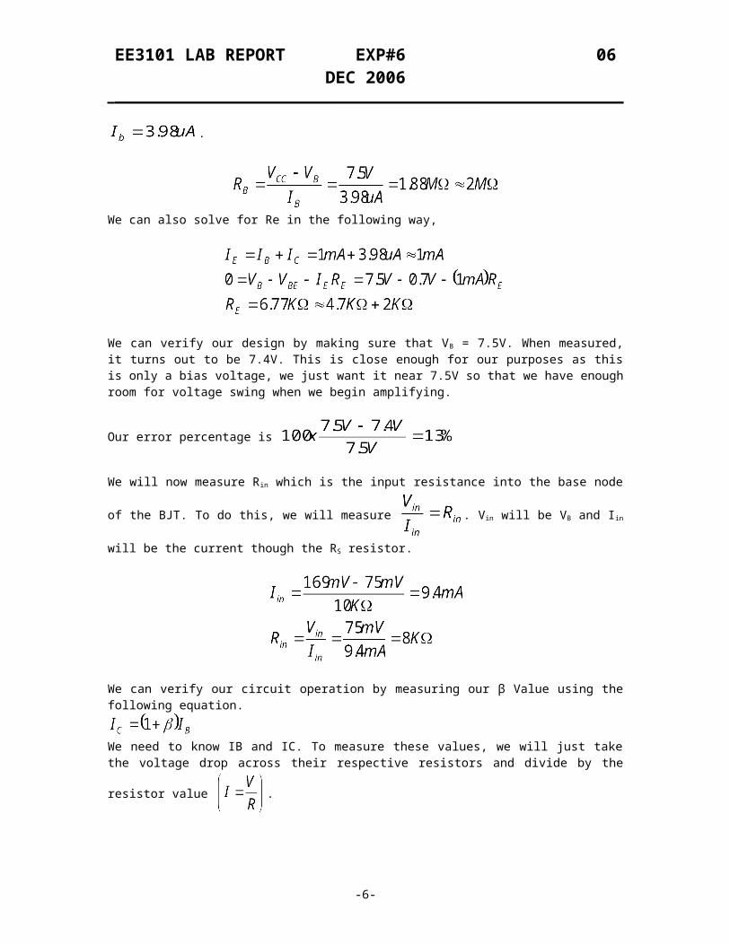
We can verify our design by making sure that VB = 7.5V. When measured, it turns out to be 7.4V. This is close enough for our purposes as this is only a bias voltage, we just want it near 7.5V so that we have enough room for voltage swing when we begin amplifying.
Our error percentage is
We will now measure Rin which is the input resistance into the base node of the BJT. To do this, we will
measure . Vin will be VB and Iin will be the current though the RS resistor.
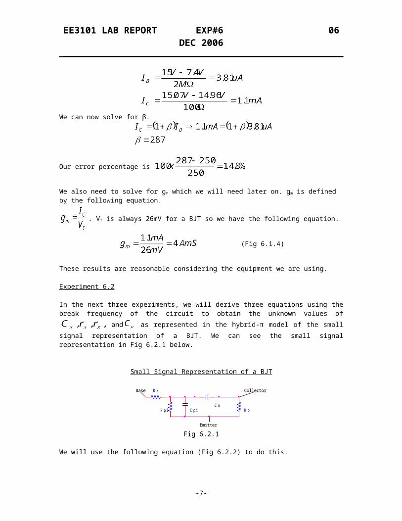
We can verify our circuit operation by measuring our β Value using the following equation.
We need to know IB and IC. To measure these values, we will just take the voltage drop across their
respective resistors and divide by the resistor value .
We can now solve for β.
Our error percentage is
We also need to solve for gm which we will need later on. gm is defined by the following equation.
. VT is always 26mV for a BJT so we have the following equation.
(Fig 6.1.4)
These results are reasonable considering the equipment we are using.
In the next three experiments, we will derive three equations using the break frequency of the circuit to obtain the unknown values of and as represented in the hybrid-π model of the small signal representation of a BJT. We can see the small signal representation in Fig 6.2.1 below.
Small Signal Representation of a BJT
R x
C p i
CollectorBase
R o
Emitter
C uR p i
Fig 6.2.1
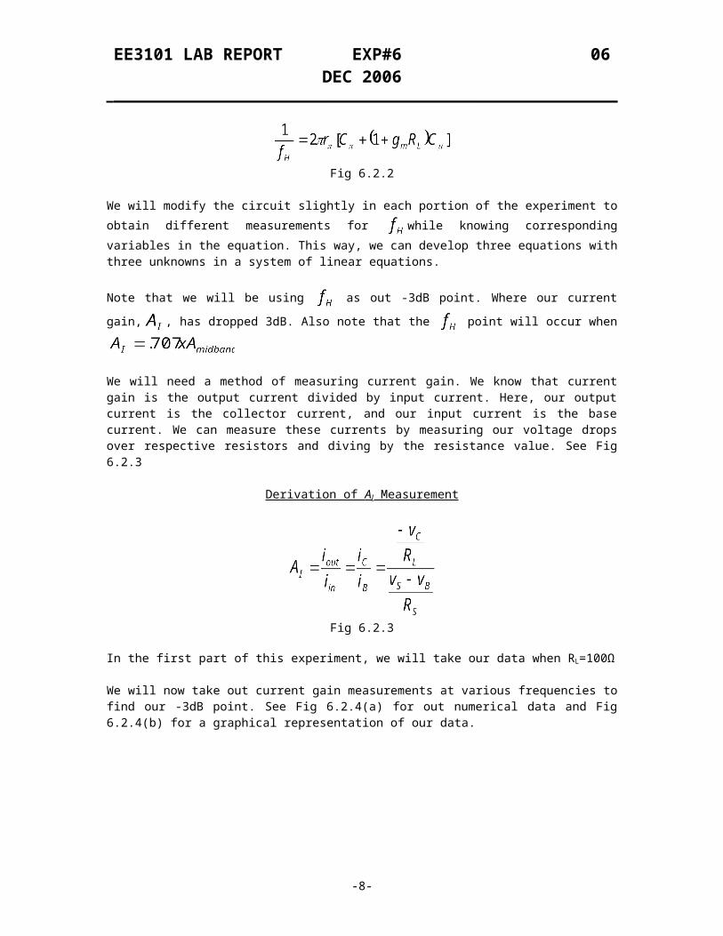
We will use the following equation (Fig 6.2.2) to do this.
Fig 6.2.2
We will modify the circuit slightly in each portion of the experiment to obtain different measurements for while knowing corresponding variables in the equation. This way, we can develop three equations with
three unknowns in a system of linear equations.
Note that we will be using as out -3dB point. Where our current gain, , has dropped 3dB. Also note
that the point will occur when
We will need a method of measuring current gain. We know that current gain is the output current divided by input current. Here, our output current is the collector current, and our input current is the base current. We can measure these currents by measuring our voltage drops over respective resistors and diving by the resistance value. See Fig 6.2.3
Derivation of A I Measurement
Fig 6.2.3
In the first part of this experiment, we will take our data when RL=100Ω
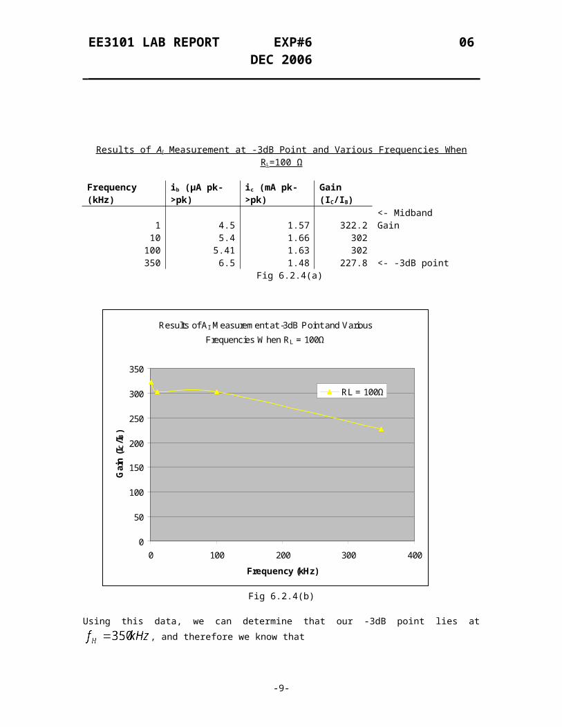
We will now take out current gain measurements at various frequencies to find our -3dB point. See Fig 6.2.4(a) for out numerical data and Fig 6.2.4(b) for a graphical representation of our data.
by plugging measured values into our equation in Fig 6.2.2.We will use Fig 6.2.5 later on when we solve for our unknowns.
Experiment 6.3
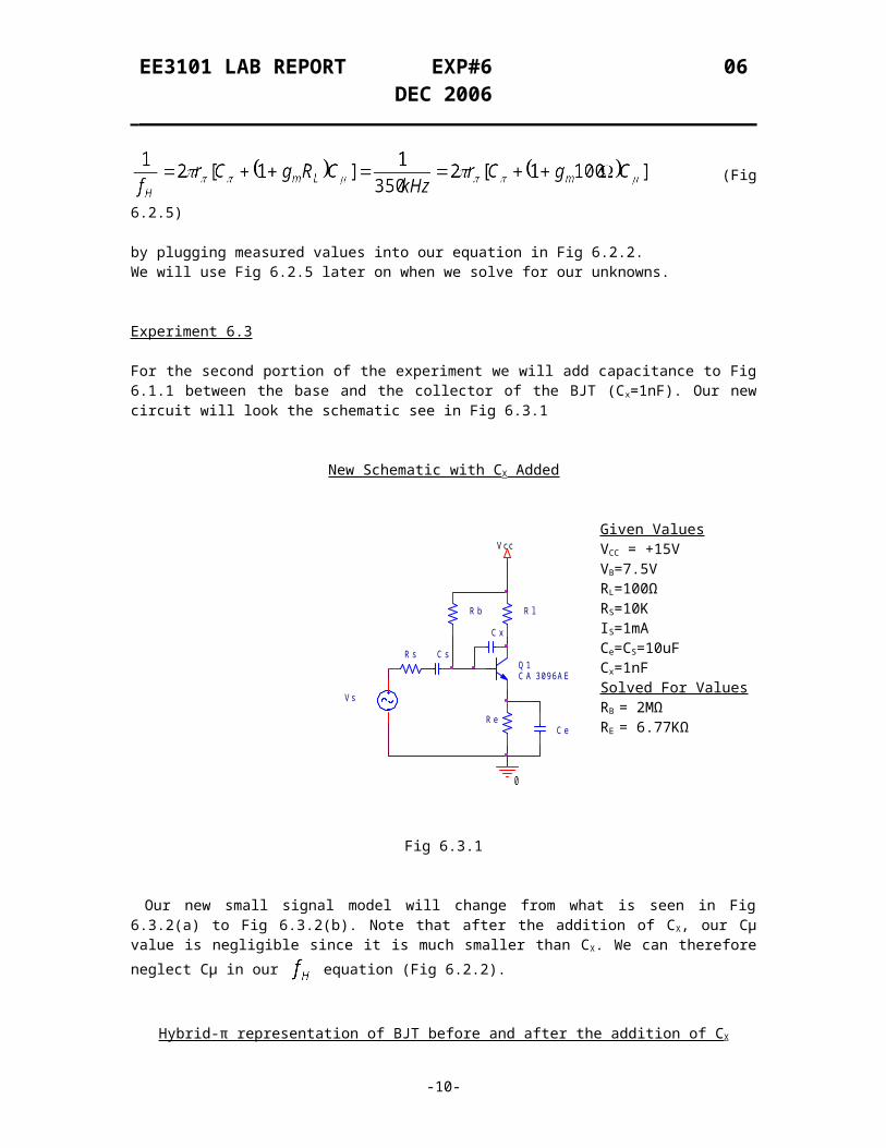
For the second portion of the experiment we will add capacitance to Fig 6.1.1 between the base and the collector of the BJT (Cx=1nF). Our new circuit will look the schematic see in Fig 6.3.1
New Schematic with CX Added
Given ValuesVCC = +15VVB=7.5VRL=100ΩRS=10KIS=1mACe=CS=10uFCx=1nFSolved For ValuesRB = 2MΩRE = 6.77KΩ
Fig 6.3.1
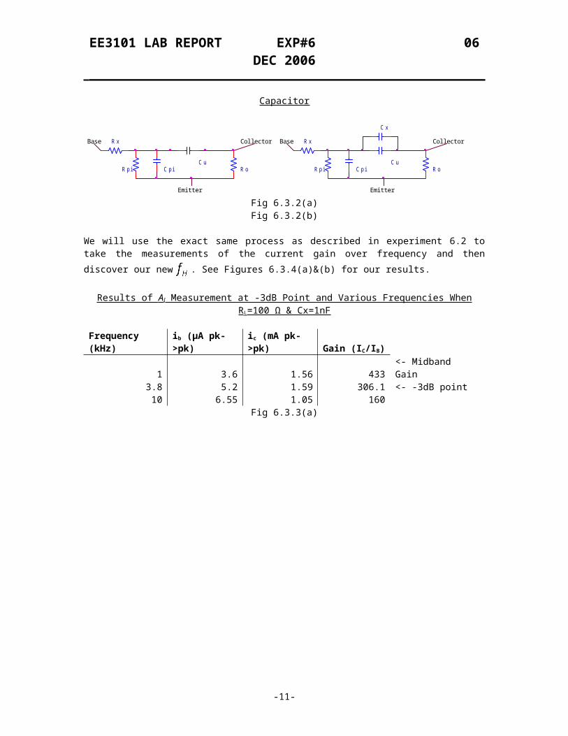
Our new small signal model will change from what is seen in Fig 6.3.2(a) to Fig 6.3.2(b). Note that after the addition of CX, our Cµ value is negligible since it is much smaller than CX. We can therefore neglect Cµ in our equation (Fig 6.2.2).
Hybrid-π representation of BJT before and after the addition of CX Capacitor
R x
C p i
CollectorBase
R o
Emitter
C uR p i
R x
C x
C p i
CollectorBase
R o
Emitter
C uR p i
Fig 6.3.2(a) Fig 6.3.2(b)
We will use the exact same process as described in experiment 6.2 to take the measurements of the current gain over frequency and then discover our new . See Figures 6.3.4(a)&(b) for our results.
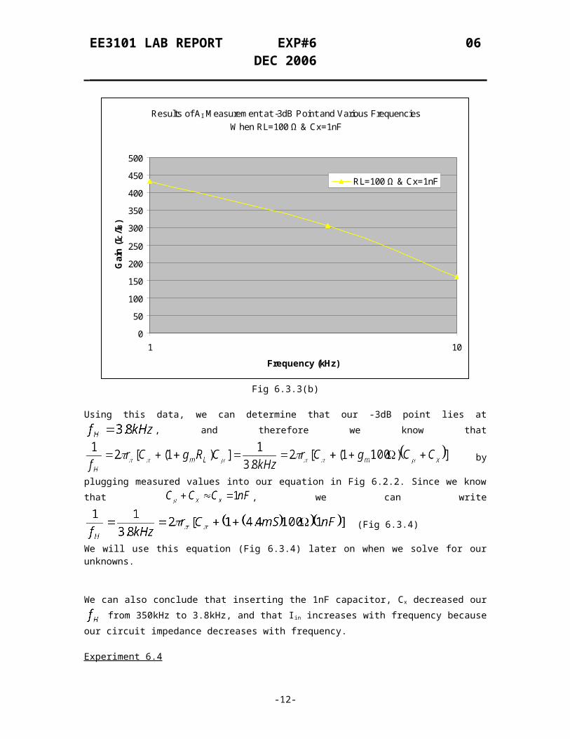
Results of A I Measurement at -3dB Point and Various Frequencies When RL=100 Ω & Cx=1nF
Frequency (kHz) ib (µA pk->pk) ic (mA pk->pk) Gain (IC/IB)1 3.6 1.56 433 <- Midband Gain
3.8 5.2 1.59 306.1 <- -3dB point10 6.55 1.05 160
Fig 6.3.3(a)
Results of AI Measurement at -3dB Point and Various Frequencies
When RL=100 Ω & Cx=1nF
0
50
100
150
200
250
300
350
400
450
500
1 10
Frequency (kHz)
Gai
n (
I C/I
B)
RL=100 Ω & Cx=1nF
Fig 6.3.3(b)
Using this data, we can determine that our -3dB point lies at , and therefore we know that
by plugging
measured values into our equation in Fig 6.2.2. Since we know that , we can write
(Fig 6.3.4)
We will use this equation (Fig 6.3.4) later on when we solve for our unknowns.
We can also conclude that inserting the 1nF capacitor, Cx decreased our from 350kHz to 3.8kHz, and that Iin increases with frequency because our circuit impedance decreases with frequency.
Experiment 6.4
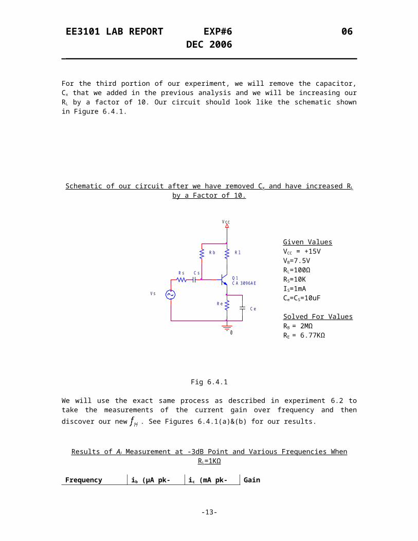
For the third portion of our experiment, we will remove the capacitor, Cx that we added in the previous analysis and we will be increasing our RL by a factor of 10. Our circuit should look like the schematic shown in Figure 6.4.1.
Schematic of our circuit after we have removed Cx and have increased RL by a Factor of 10.
Given ValuesVCC = +15VVB=7.5VRL=100ΩRS=10KIS=1mACe=CS=10uF
Solved For ValuesRB = 2MΩRE = 6.77KΩ
Fig 6.4.1
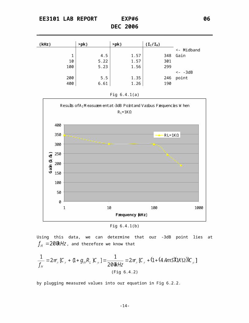
We will use the exact same process as described in experiment 6.2 to take the measurements of the current gain over frequency and then discover our new . See Figures 6.4.1(a)&(b) for our results.
Results of A I Measurement at -3dB Point and Various Frequencies When RL=1KΩ
Frequency (kHz) ib (µA pk->pk) ic (mA pk->pk) Gain (IC/IB)1 4.5 1.57 348 <- Midband Gain
Results of AI Measurement at -3dB Point and Various Frequencies When
RL=1KΩ
0
50
100
150
200
250
300
350
400
1 10 100 1000
Frequency (kHz)
Gai
n (
I C/I
B)
RL=1KΩ
Fig 6.4.1(b)
Using this data, we can determine that our -3dB point lies at , and therefore we know that
(Fig 6.4.2)
by plugging measured values into our equation in Fig 6.2.2.
We can conclude that increasing the load resistor, RL decreased our from 350kHz to 200kHz. This is most likely because increasing the load resistor will increase the input impedance and therefore slow the charging time of the capacitors. This reduces the gain because the capacitors cannot charge as quickly as before at higher frequencies.
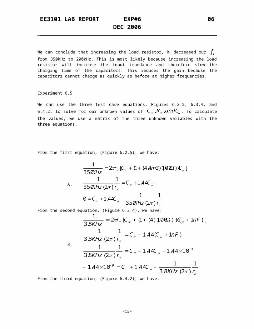
Experiment 6.5
We can use the three test case equations, Figures 6.2.5, 6.3.4, and 6.4.2, to solve for our unknown values of . To calculate the values, we use a matrix of the three unknown variables with the three
From the second equation, (Figure 6.3.4), we have:
B.
From the third equation, (Figure 6.4.2), we have:
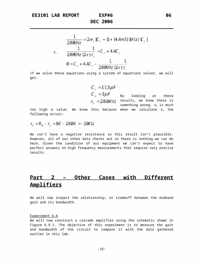
C.
If we solve these equations using a system of equations solver, we will get:
By looking at these results, we know there is something wrong. rπ is much too high a value. We know this because when we calculate rx the following occurs:
We can’t have a negative resistance so this result isn’t plausible. However, all of our other data checks out so there is nothing we can do here. Given the condition of our equipment we can’t expect to have perfect answers on high frequency measurements that require very precise results.
We will now inspect the relationship, or tradeoff between the midband gain and its bandwidth.
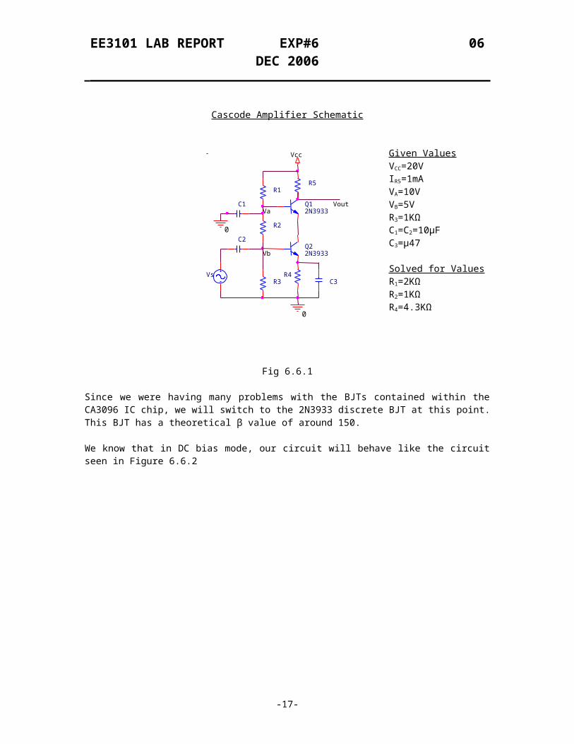
Experiment 6.6We will now construct a cascade amplifier using the schematic shown in Figure 6.6.1. The objective of this experiment is to measure the gain and bandwidth of the circuit to compare it with the data gathered earlier in this lab.
Cascode Amplifier Schematic
Given ValuesVCC=20VIR5=1mAVA=10VVB=5VR3=1KΩC1=C2=10µFC3=µ47
Solved for ValuesR1=2KΩR2=1KΩR4=4.3KΩ
Fig 6.6.1
Since we were having many problems with the BJTs contained within the CA3096 IC chip, we will switch to the 2N3933 discrete BJT at this point. This BJT has a theoretical β value of around 150.
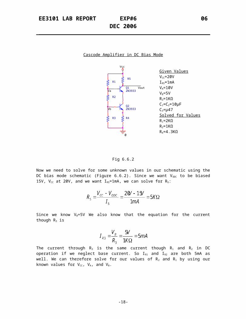
We know that in DC bias mode, our circuit will behave like the circuit seen in Figure 6.6.2
Given ValuesVCC=20VIR5=1mAVA=10VVB=5VR3=1KΩC1=C2=10µFC3=µ47Solved for ValuesR1=2KΩR2=1KΩR4=4.3KΩ
Fig 6.6.2
Now we need to solve for some unknown values in our schematic using the DC bias mode schematic (Figure 6.6.2). Since we want VODC to be biased 15V, VCC at 20V, and we want IR5=1mA, we can solve for R5:
Since we know VB=5V We also know that the equation for the current though R3 is
The current through R3 is the same current though R1 and R2 in DC operation if we neglect base current. So IR1 and IR2 are both 5mA as well. We can therefore solve for our values of R 2 and R1 by using our known values for VCC, VA, and VB.
Since the voltage at the emitter of Q2 is 5V-0.7V=4.3V, the current though R4 is 1mA during DC operation if we neglect base currents. This is because we are therefore assuming the entire right side of the amplifier has a current of 1mA.
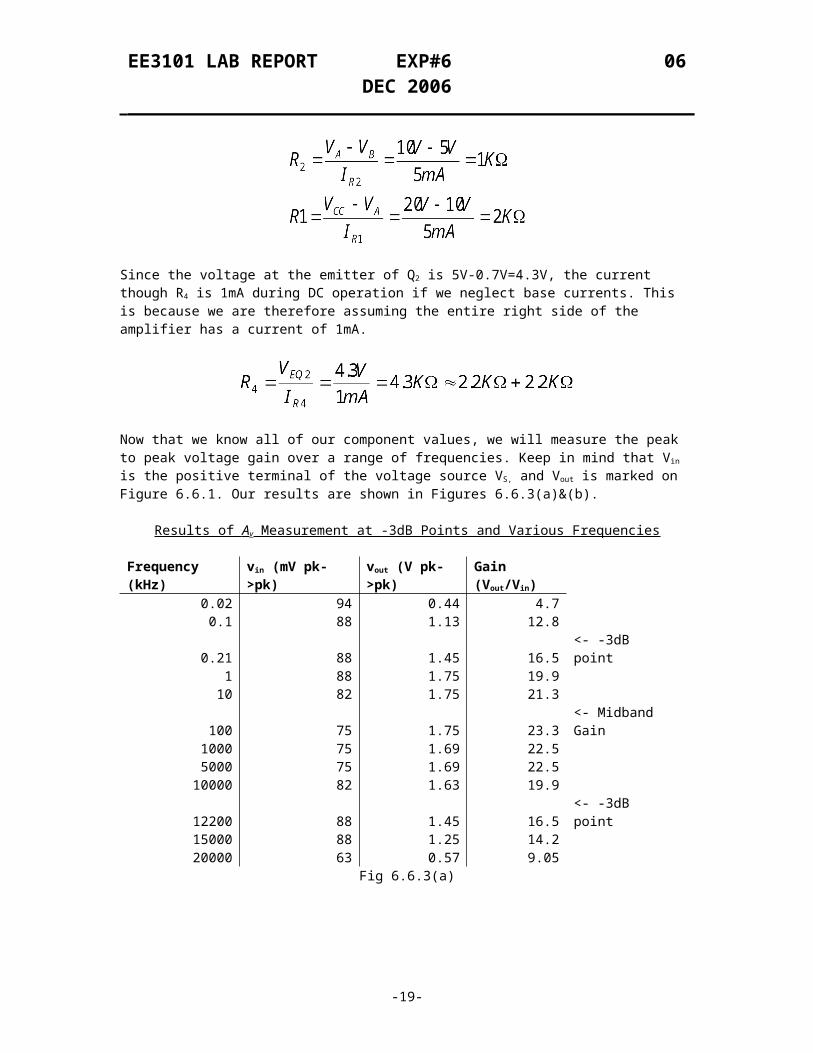
Now that we know all of our component values, we will measure the peak to peak voltage gain over a range
of frequencies. Keep in mind that Vin is the positive terminal of the voltage source VS, and Vout is marked on Figure 6.6.1. Our results are shown in Figures 6.6.3(a)&(b).
Results of A v Measurement at -3dB Points and Various Frequencies
Frequency (kHz) vin (mV pk->pk) vout (V pk->pk) Gain (Vout/Vin)0.02 94 0.44 4.7
We will now construct a CC-CB amplifier to compare with the previous cascade amplifier we analyzed in experiment 6.6. The schematic for the CC-CB amplifier is shown below in Figure 6.7.1.Note that we will be using the 2N3393 discrete transistors that were used in experiment 6.6.
CC-CB Amplifier Schematic
Given ValuesVCC = 15VVA=5VVB=5VVODC=10VICQ1=1mAIR5=1mAC1=C2=10µFC3=47µFSolved For ValuesR4=5KΩR2=5KΩR1=1MΩR3=1MΩIBQ1=IBQ2=6.6µA
Fig 6.7.1
We know that in DC bias mode, our circuit will behave like the circuit seen in Figure 6.7.2
CC-CB Amplifier in DC Bias ModeGiven ValuesVCC = 15VVA=5VVB=5VVODC=10VICQ1=1mAIR5=1mAC1=C2=10µFC3=47µFSolved For ValuesR4=5KΩR2=5KΩR1=1MΩR3=1MΩIBQ1=IBQ2=6.6µA
Fig 6.7.2Now we need to solve for some unknown values in our schematic using the DC bias mode schematic (Figure 6.7.2).
We know that VB=5V and IR5=1mA and therefore IR4=1mA if we neglect base current, so we can solve for the resistance of R4
We can also solve for R2 in the same fashion.
We also know that VBQ1 and VBQ2 are both 5V+.7V=5.7V because of VBE=.7V so we can solve for both R1
and R3 by first solving for IBQ1 and IBQ2.
We can now solve for R1 and R3.
We will now measure our peak to peak voltage gain over various frequencies just as we did in experiment 6.6. Once again, our input voltage is the positive terminal of VS and our Vout terminal is shown on Figure 6.7.1. Our results are shown in Figures 6.7.3(a)&(b).
Results of A v Measurement at -3dB Points and Various Frequencies
Frequency (kHz) vin (mV pk->pk) vout (V pk->pk) Gain (Vout/Vin)0.02 108 2.69 24.9
Results of Av Measurement at -3dB Points and Various Frequencies
0
20
40
60
80
100
120
0.01 0.1 1 10 100 1000 10000
Frequency (kHz)
Gai
n (
Vo
ut/V
in)
CC-CB Amplifier
Fig 6.7.3(b)Using this data, we can determine that our -3dB points lie at and , and
therefore we know that our bandwidth is we also know that our midband gain is 79.8 V/V.
Experiment 6.8
From the former experiments we can notice that the larger the gain will be, the smaller the bandwidth turns out to be. If we multiply our midband gain by out bandwidth, we can obtain a measurement called the gain-bandwidth product. This measurement is the relative effectiveness of the amplifier. Since we already know we can sacrifice one quality for the other, the gain-bandwidth product will tell the amount of both qualities we can have. Figure 6.8.1 is a set of the results of the previous experiments.
Previous Results and Calculated Gain-Bandwidth Products.Cascode CC-CB
Midband Gain 23.3 112.9Bandwidth 12.2M 1.31M
Gain-Bandwidth Product 284.2M 237.1MFig 6.8.1
Our percent deviation is
We can see that the gain-bandwidth product of the cascode amplifier was larger, this means that the cascade amplifier was slightly more efficient than the CC-CB amplifier. The main idea, however, is that even though the basic schematics of the circuit were different, we can see a similar trade off in gain and
First we calculated β as 287 of the common-emitter amplifier. We then obtained three equations relating the unknown values of the Hybrid-π Model and the cutoff frequencies that were gathered at the 3dB (70.7%) point through modifying the CE amplifier with three different composition. We added a capacitor parallel with to change the effect of the capacitance, and then changed the value of RL to see the effect of the load resistance and the break frequency. From a calculation using a matrix of the three equations, with the three unknown values, we got , , as a
result. The values of and seem to reasonable values, however, was bigger than expected. We know this because when we calculate rx it turns out to be a negative value (-20KΩ) which isn’t possible.
Next we measured the voltage gain of the cascode amplifier design and the CC-CB amplifier design. With the voltage gain we were able to calculate the break frequency of the amplifiers and the bandwidth of them. By comparing the data of the two, we were able to check the inverse proportional relationship between the midband gain and bandwidth. See Figure 6.8.1 for comparison of the two different amplifiers. With an amplifier that has a greater gain; it is hard to expect a large bandwidth. When designing an amplifier we must consider the trade off of the two core aspects within the amplifier.
We have successfully gathered the information on how to interpret the high frequency response of the Hybrid-π Model and characteristic of the model. This information should be used on further amplifiers’ analysis and designing projects to gather more accurate results.