EECS 16A Designing Information Devices and Systems I Fall 2017 Midterm 2 Midterm 2 Solution PRINT your student ID: PRINT AND SIGN your name: , (last name) (first name) (signature) PRINT your discussion section and GSI(s) (the one you attend): Name and SID of the person to your left: Name and SID of the person to your right: Name and SID of the person in front of you: Name and SID of the person behind you: 1. What do you enjoy most about EE16A? (1 Point) 2. What other courses are you taking this semester? (1 Point) Do not turn this page until the proctor tells you to do so. You may work on the questions above. EECS 16A, Fall 2017, Midterm 2 1
Transcript
EECS 16A Designing Information Devices and Systems IFall 2017 Midterm 2
Midterm 2 Solution
PRINT your student ID:
PRINT AND SIGN your name: ,(last name) (first name) (signature)
PRINT your discussion section and GSI(s) (the one you attend):
Name and SID of the person to your left:
Name and SID of the person to your right:
Name and SID of the person in front of you:
Name and SID of the person behind you:
1. What do you enjoy most about EE16A? (1 Point)
2. What other courses are you taking this semester? (1 Point)
Do not turn this page until the proctor tells you to do so. You may work on the questions above.
EECS 16A, Fall 2017, Midterm 2 1
PRINT your name and student ID:
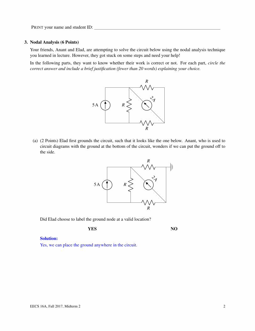
3. Nodal Analysis (6 Points)
Your friends, Anant and Elad, are attempting to solve the circuit below using the nodal analysis techniqueyou learned in lecture. However, they got stuck on some steps and need your help!
In the following parts, they want to know whether their work is correct or not. For each part, circle thecorrect answer and include a brief justification (fewer than 20 words) explaining your choice.
5A R
R
R
2A
(a) (2 Points) Elad first grounds the circuit, such that it looks like the one below. Anant, who is used tocircuit diagrams with the ground at the bottom of the circuit, wonders if we can put the ground off tothe side.
5A R
R
R
2A
Did Elad choose to label the ground node at a valid location?
YES NO
Solution:Yes, we can place the ground anywhere in the circuit.
EECS 16A, Fall 2017, Midterm 2 2
PRINT your name and student ID:
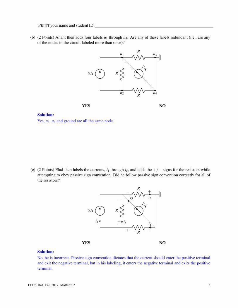
(b) (2 Points) Anant then adds four labels u1 through u4. Are any of these labels redundant (i.e., are anyof the nodes in the circuit labeled more than once)?
5A
u1
R
u2
R u3
u4R
2A
YES NO
Solution:Yes, u3, u4 and ground are all the same node.
(c) (2 Points) Elad then labels the currents, i1 through i5, and adds the +/− signs for the resistors whileattempting to obey passive sign convention. Did he follow passive sign convention correctly for all ofthe resistors?
5A
i1
R
−
+ i5
R− +
i2
R−+
i4
2A
i3
YES NO
Solution:No, he is incorrect. Passive sign convention dictates that the current should enter the positive terminaland exit the negative terminal, but in his labeling, it enters the negative terminal and exits the positiveterminal.
EECS 16A, Fall 2017, Midterm 2 3
PRINT your name and student ID:
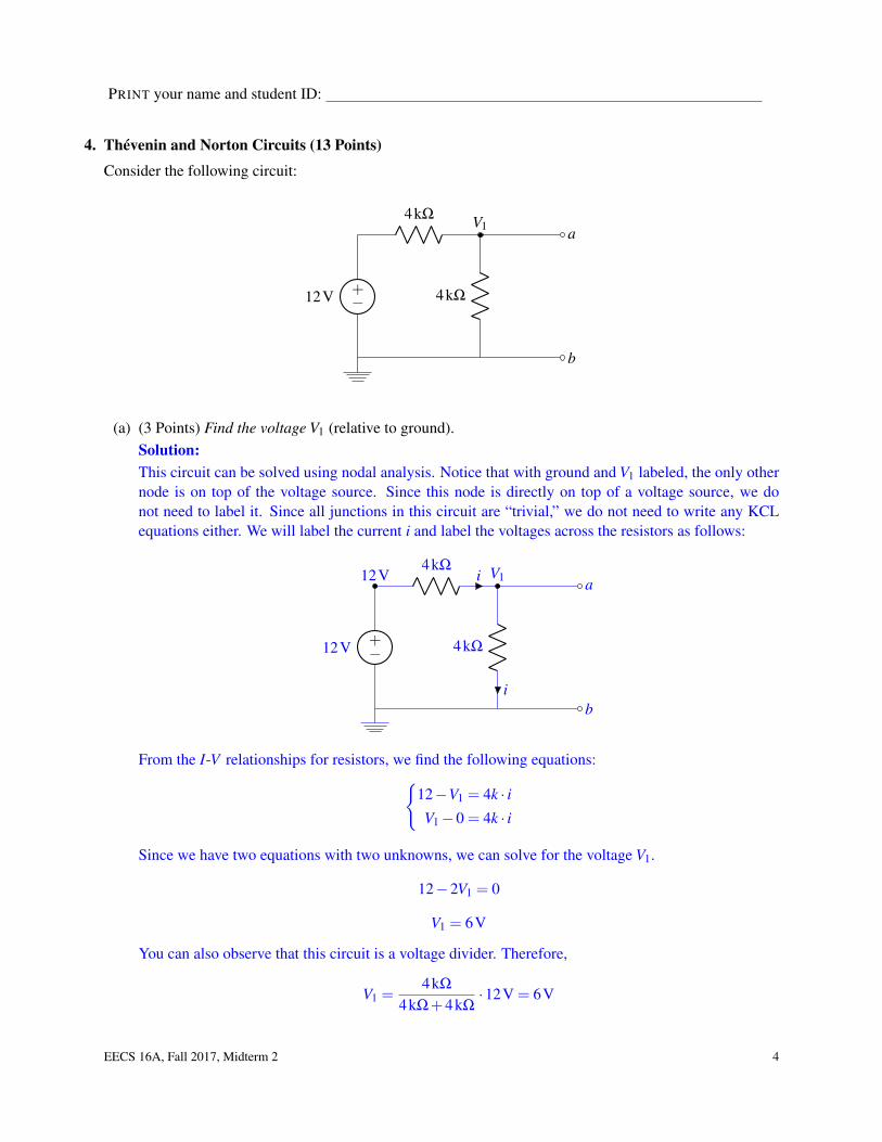
4. Thévenin and Norton Circuits (13 Points)
Consider the following circuit:
−+12V
4kΩ
4kΩ
V1 a
b
(a) (3 Points) Find the voltage V1 (relative to ground).Solution:This circuit can be solved using nodal analysis. Notice that with ground and V1 labeled, the only othernode is on top of the voltage source. Since this node is directly on top of a voltage source, we donot need to label it. Since all junctions in this circuit are “trivial,” we do not need to write any KCLequations either. We will label the current i and label the voltages across the resistors as follows:
12V
−+12V
4kΩi
4kΩ
i
V1 a
b
From the I-V relationships for resistors, we find the following equations:12−V1 = 4k · iV1−0 = 4k · i
Since we have two equations with two unknowns, we can solve for the voltage V1.
12−2V1 = 0
V1 = 6V
You can also observe that this circuit is a voltage divider. Therefore,
V1 =4kΩ
4kΩ+4kΩ·12V = 6V
EECS 16A, Fall 2017, Midterm 2 4
PRINT your name and student ID:
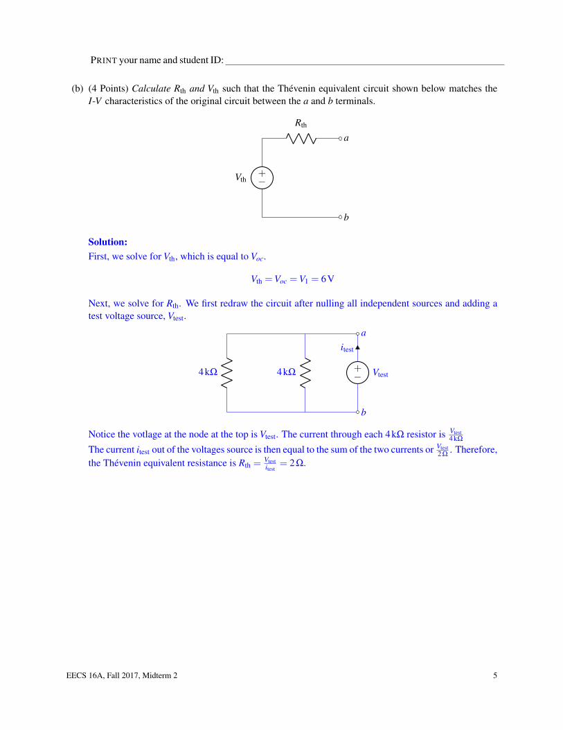
(b) (4 Points) Calculate Rth and Vth such that the Thévenin equivalent circuit shown below matches theI-V characteristics of the original circuit between the a and b terminals.
aRth
−+Vth
b
Solution:First, we solve for Vth, which is equal to Voc.
Vth =Voc =V1 = 6V
Next, we solve for Rth. We first redraw the circuit after nulling all independent sources and adding atest voltage source, Vtest.
a
4kΩ
b
4kΩ −+ Vtest
itest
Notice the votlage at the node at the top is Vtest. The current through each 4kΩ resistor is Vtest4kΩ
The current itest out of the voltages source is then equal to the sum of the two currents or Vtest2Ω
. Therefore,the Thévenin equivalent resistance is Rth =
Vtestitest
= 2Ω.
EECS 16A, Fall 2017, Midterm 2 5
PRINT your name and student ID:
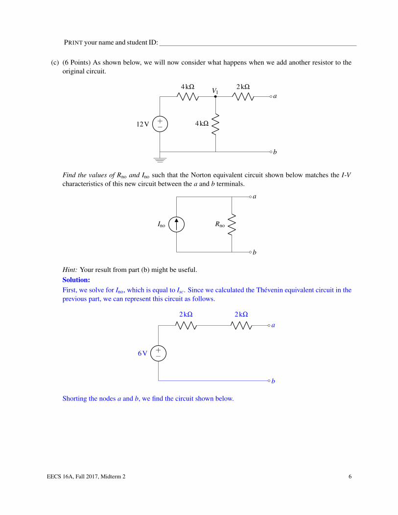
(c) (6 Points) As shown below, we will now consider what happens when we add another resistor to theoriginal circuit.
−+12V
4kΩ
4kΩ
V12kΩ
a
b
Find the values of Rno and Ino such that the Norton equivalent circuit shown below matches the I-Vcharacteristics of this new circuit between the a and b terminals.
a
b
Ino Rno
Hint: Your result from part (b) might be useful.Solution:First, we solve for Ino, which is equal to Isc. Since we calculated the Thévenin equivalent circuit in theprevious part, we can represent this circuit as follows.
a2kΩ2kΩ
−+6V
b
Shorting the nodes a and b, we find the circuit shown below.
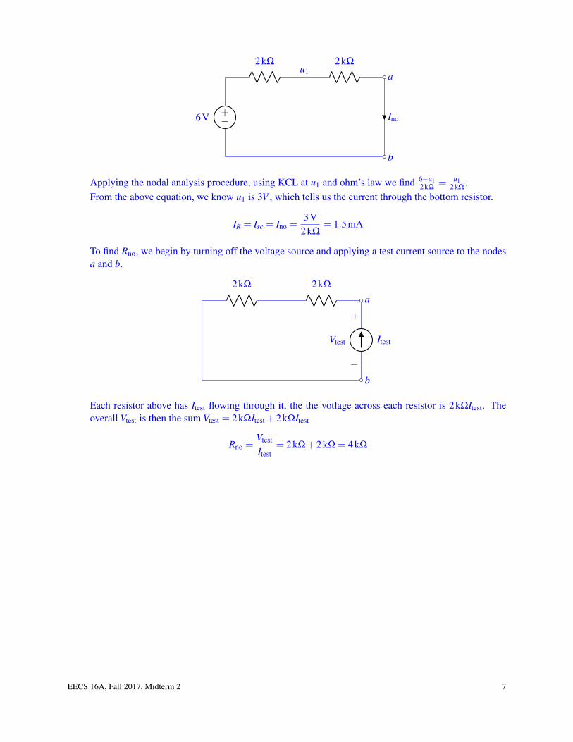
EECS 16A, Fall 2017, Midterm 2 6
a2kΩ
u12kΩ
−+6V
b
Ino
Applying the nodal analysis procedure, using KCL at u1 and ohm’s law we find 6−u12kΩ
= u12kΩ
.From the above equation, we know u1 is 3V , which tells us the current through the bottom resistor.
IR = Isc = Ino =3V
2kΩ= 1.5mA
To find Rno, we begin by turning off the voltage source and applying a test current source to the nodesa and b.
a2kΩ2kΩ
b
Itest
+
−
Vtest
Each resistor above has Itest flowing through it, the the votlage across each resistor is 2kΩItest. Theoverall Vtest is then the sum Vtest = 2kΩItest +2kΩItest
Rno =Vtest
Itest= 2kΩ+2kΩ = 4kΩ
EECS 16A, Fall 2017, Midterm 2 7
PRINT your name and student ID:
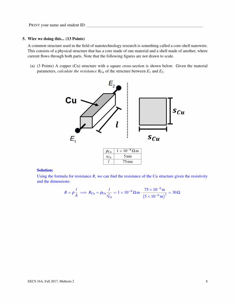
5. Wire we doing this... (13 Points)
A common structure used in the field of nanotechnology research is something called a core-shell nanowire.This consists of a physical structure that has a core made of one material and a shell made of another, wherecurrent flows through both parts. Note that the following figures are not drawn to scale.
(a) (3 Points) A copper (Cu) structure with a square cross-section is shown below. Given the materialparameters, calculate the resistance RCu of the structure between E1 and E2.
ρCu 1×10⁻⁸ ΩmsCu 5nml 75nm
Solution:Using the formula for resistance R, we can find the resistance of the Cu structure given the resistivityand the dimensions:
R = ρlA
=⇒ RCu = ρCul
s2Cu
= 1×10−8Ωm · 75×10−9 m(
5×10⁻⁹ m)2 = 30Ω
EECS 16A, Fall 2017, Midterm 2 8
PRINT your name and student ID:
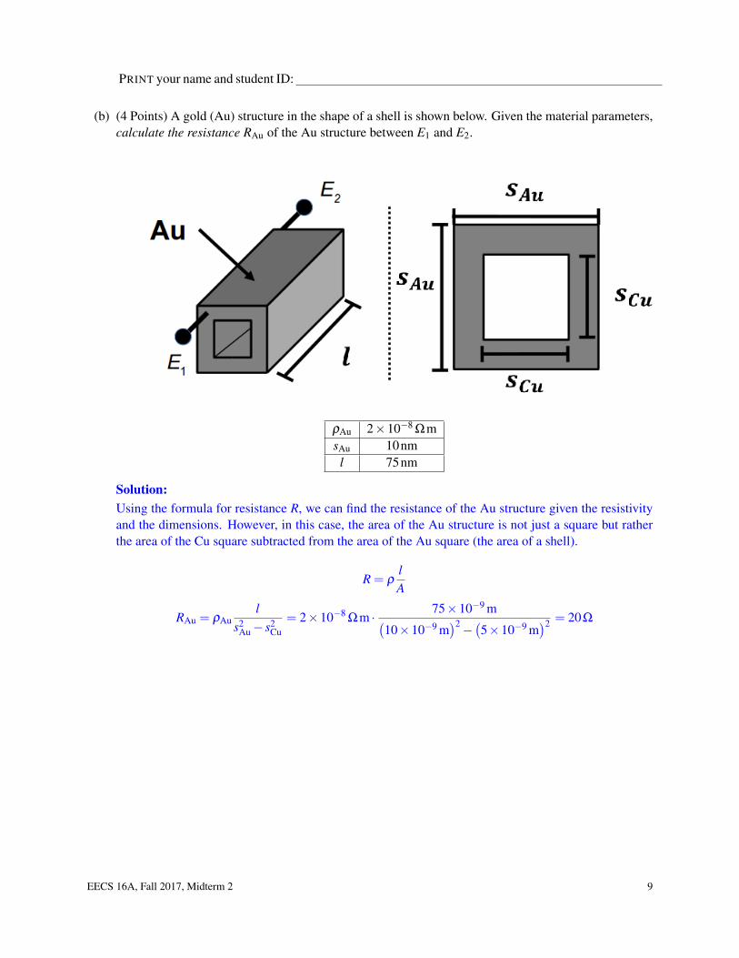
(b) (4 Points) A gold (Au) structure in the shape of a shell is shown below. Given the material parameters,calculate the resistance RAu of the Au structure between E1 and E2.
ρAu 2×10⁻⁸ ΩmsAu 10nml 75nm
Solution:Using the formula for resistance R, we can find the resistance of the Au structure given the resistivityand the dimensions. However, in this case, the area of the Au structure is not just a square but ratherthe area of the Cu square subtracted from the area of the Au square (the area of a shell).
R = ρlA
RAu = ρAul
s2Au− s2
Cu= 2×10−8
Ωm · 75×10−9 m(10×10−9 m
)2−(5×10⁻⁹ m
)2 = 20Ω
EECS 16A, Fall 2017, Midterm 2 9
PRINT your name and student ID:
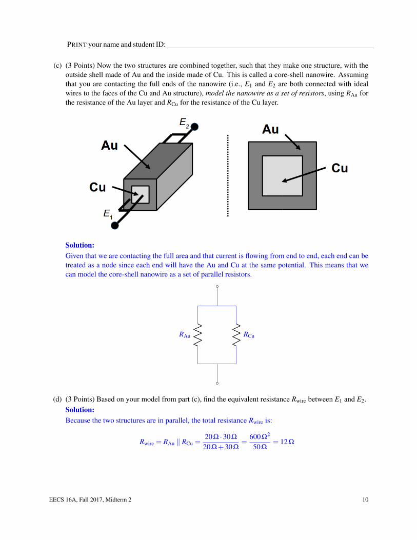
(c) (3 Points) Now the two structures are combined together, such that they make one structure, with theoutside shell made of Au and the inside made of Cu. This is called a core-shell nanowire. Assumingthat you are contacting the full ends of the nanowire (i.e., E1 and E2 are both connected with idealwires to the faces of the Cu and Au structure), model the nanowire as a set of resistors, using RAu forthe resistance of the Au layer and RCu for the resistance of the Cu layer.
Solution:Given that we are contacting the full area and that current is flowing from end to end, each end can betreated as a node since each end will have the Au and Cu at the same potential. This means that wecan model the core-shell nanowire as a set of parallel resistors.
RAu RCu
(d) (3 Points) Based on your model from part (c), find the equivalent resistance Rwire between E1 and E2.Solution:Because the two structures are in parallel, the total resistance Rwire is:
Rwire = RAu ‖ RCu =20Ω ·30Ω
20Ω+30Ω=
600Ω2
50Ω= 12Ω
EECS 16A, Fall 2017, Midterm 2 10
PRINT your name and student ID:
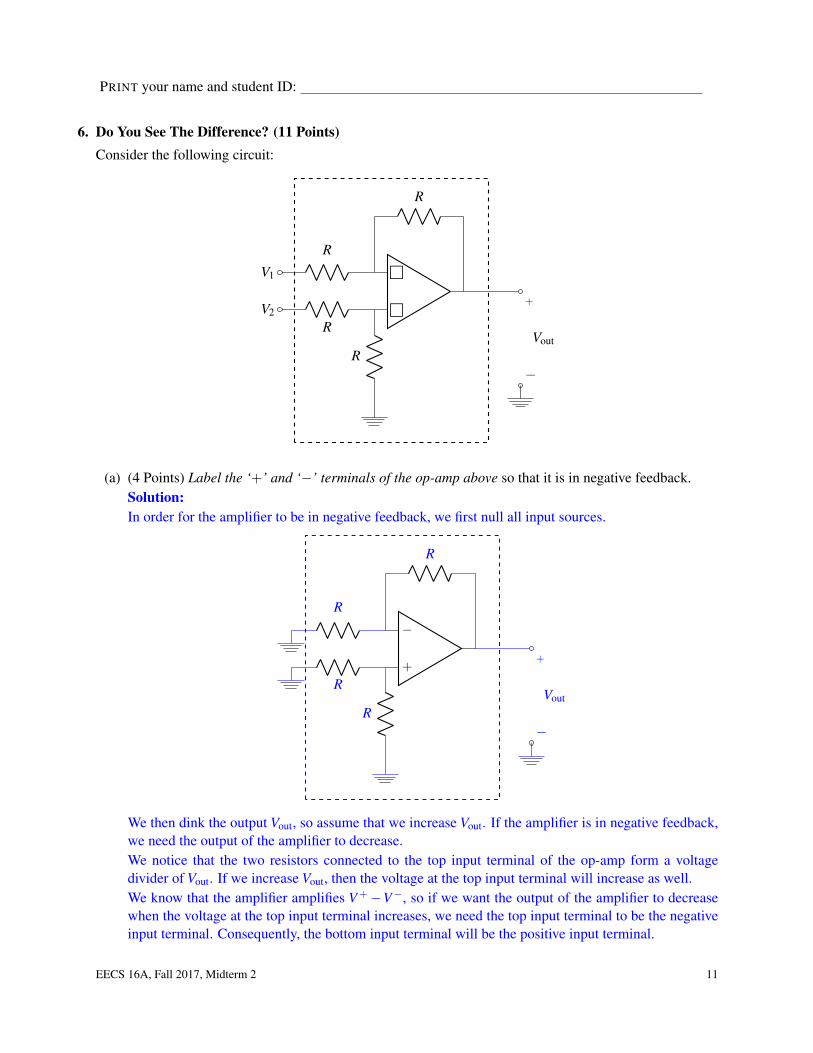
6. Do You See The Difference? (11 Points)Consider the following circuit:
RV2
R
R
V1
R
+
−
Vout
(a) (4 Points) Label the ‘+’ and ‘−’ terminals of the op-amp above so that it is in negative feedback.Solution:In order for the amplifier to be in negative feedback, we first null all input sources.
−
+
R
R
R
R
+
−
Vout
We then dink the output Vout, so assume that we increase Vout. If the amplifier is in negative feedback,we need the output of the amplifier to decrease.We notice that the two resistors connected to the top input terminal of the op-amp form a voltagedivider of Vout. If we increase Vout, then the voltage at the top input terminal will increase as well.We know that the amplifier amplifies V+−V−, so if we want the output of the amplifier to decreasewhen the voltage at the top input terminal increases, we need the top input terminal to be the negativeinput terminal. Consequently, the bottom input terminal will be the positive input terminal.
EECS 16A, Fall 2017, Midterm 2 11
−
+
RV2
R
R
V1
R
+
−
Vout
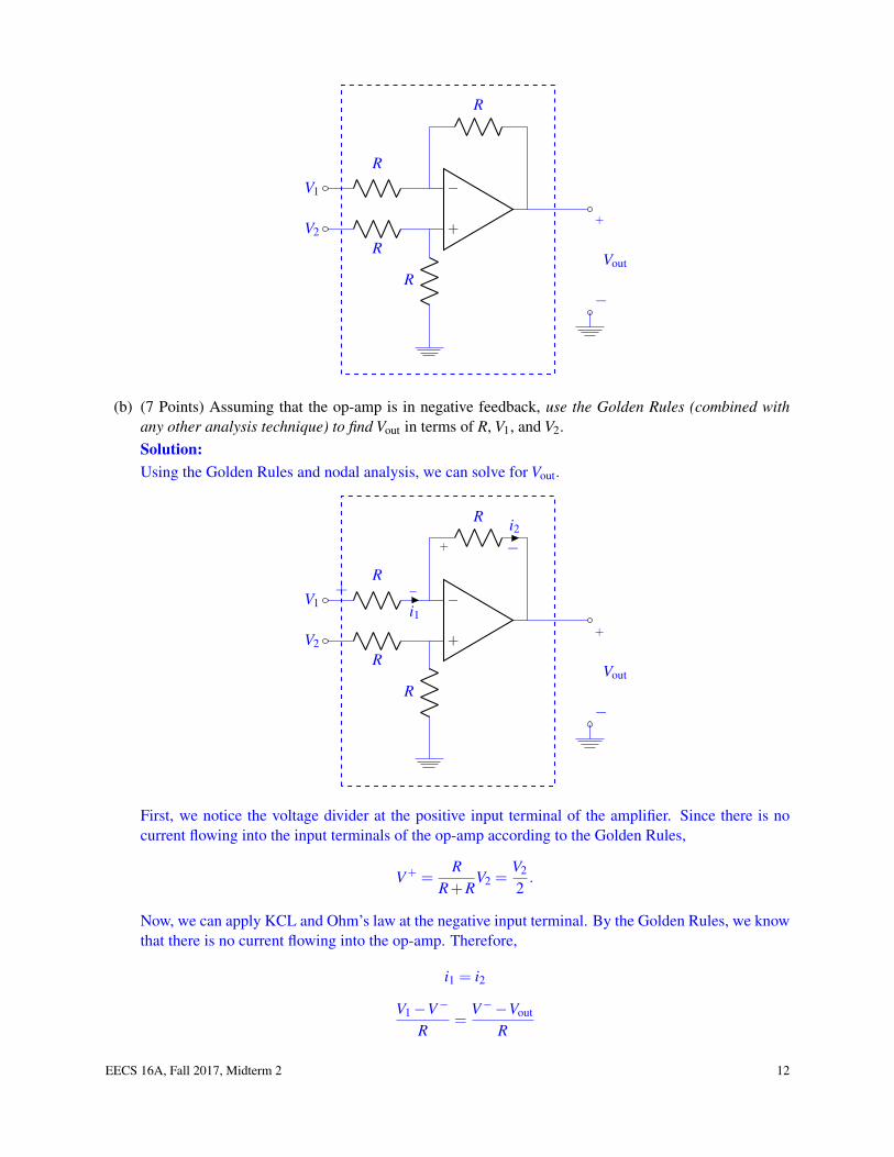
(b) (7 Points) Assuming that the op-amp is in negative feedback, use the Golden Rules (combined withany other analysis technique) to find Vout in terms of R, V1, and V2.Solution:Using the Golden Rules and nodal analysis, we can solve for Vout.
−
+
RV2
R
R−+
i1V1
R
+ −i2
+
−
Vout
First, we notice the voltage divider at the positive input terminal of the amplifier. Since there is nocurrent flowing into the input terminals of the op-amp according to the Golden Rules,
V+ =R
R+RV2 =
V2
2.
Now, we can apply KCL and Ohm’s law at the negative input terminal. By the Golden Rules, we knowthat there is no current flowing into the op-amp. Therefore,
i1 = i2
V1−V−
R=
V−−Vout
R
EECS 16A, Fall 2017, Midterm 2 12
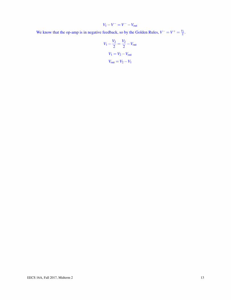
V1−V− =V−−Vout
We know that the op-amp is in negative feedback, so by the Golden Rules, V− =V+ = V22 .
V1−V2
2=
V2
2−Vout
V1 =V2−Vout
Vout =V2−V1
EECS 16A, Fall 2017, Midterm 2 13
PRINT your name and student ID:
7. A New Feature You Didn’t Even Know You Wanted! (14 Points)
An up-and-coming computer company, Orange Inc., is trying to design a touchscreen bar to incorporate intotheir new laptop, right above the keyboard. Let’s help them analyze their existing design to see where theirdesign has gone wrong!
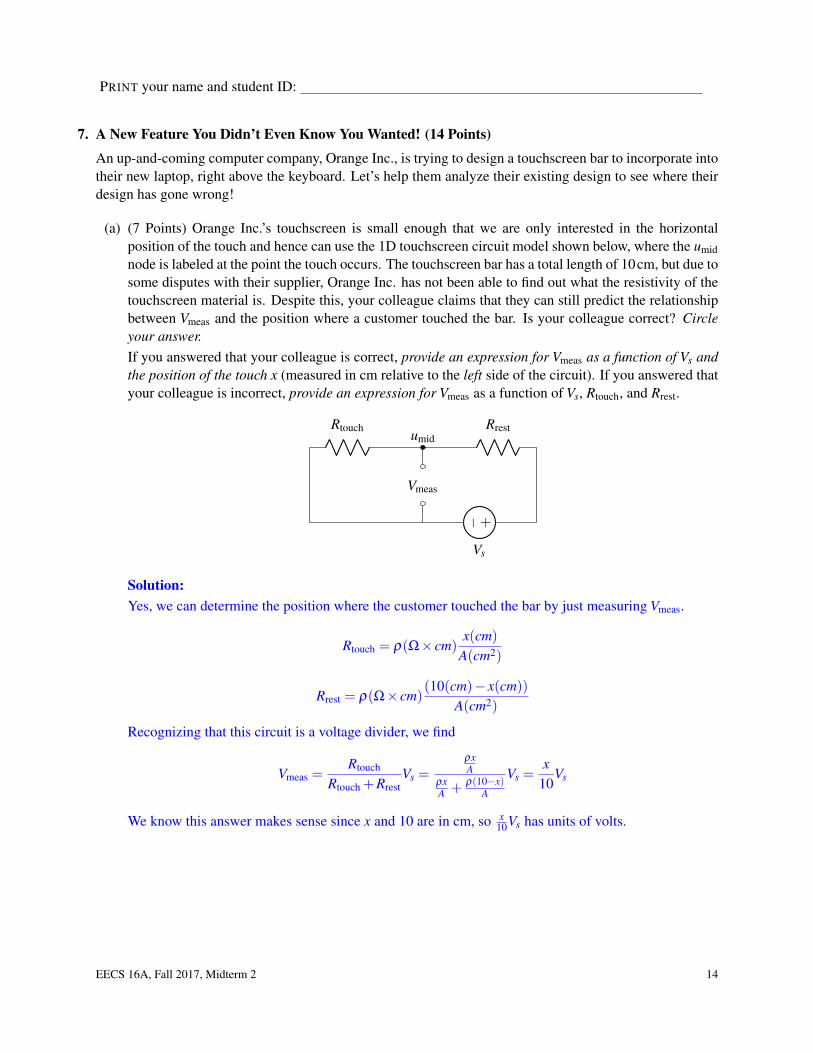
(a) (7 Points) Orange Inc.’s touchscreen is small enough that we are only interested in the horizontalposition of the touch and hence can use the 1D touchscreen circuit model shown below, where the umidnode is labeled at the point the touch occurs. The touchscreen bar has a total length of 10cm, but due tosome disputes with their supplier, Orange Inc. has not been able to find out what the resistivity of thetouchscreen material is. Despite this, your colleague claims that they can still predict the relationshipbetween Vmeas and the position where a customer touched the bar. Is your colleague correct? Circleyour answer.If you answered that your colleague is correct, provide an expression for Vmeas as a function of Vs andthe position of the touch x (measured in cm relative to the left side of the circuit). If you answered thatyour colleague is incorrect, provide an expression for Vmeas as a function of Vs, Rtouch, and Rrest.
− +
Vs
Rrestumid
Vmeas
Rtouch
Solution:Yes, we can determine the position where the customer touched the bar by just measuring Vmeas.
Rtouch = ρ(Ω× cm)x(cm)
A(cm2)
Rrest = ρ(Ω× cm)(10(cm)− x(cm))
A(cm2)
Recognizing that this circuit is a voltage divider, we find
Vmeas =Rtouch
Rtouch +RrestVs =
ρxA
ρxA + ρ(10−x)
A
Vs =x
10Vs
We know this answer makes sense since x and 10 are in cm, so x10Vs has units of volts.
EECS 16A, Fall 2017, Midterm 2 14
PRINT your name and student ID:
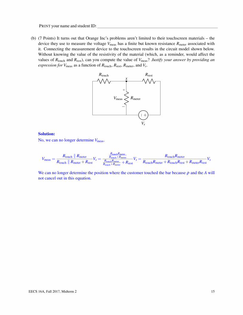
(b) (7 Points) It turns out that Orange Inc’s problems aren’t limited to their touchscreen materials – thedevice they use to measure the voltage Vmeas has a finite but known resistance Rmeter associated withit. Connecting the measurement device to the touchscreen results in the circuit model shown below.Without knowing the value of the resistivity of the material (which, as a reminder, would affect thevalues of Rtouch and Rrest), can you compute the value of Vmeas? Justify your answer by providing anexpression for Vmeas as a function of Rtouch, Rrest, Rmeter, and Vs.
− +
Vs
Rrestx
Rmeter
+
−
Vmeas
Rtouch
Solution:No, we can no longer determine Vmeas.
Vmeas =Rtouch ‖ Rmeter
Rtouch ‖ Rmeter +RrestVs =
RtouchRmeterRtouch+Rmeter
RtouchRmeterRtouch+Rmeter
+RrestVs =
RtouchRmeter
RtouchRmeter +RtouchRrest +RmeterRrestVs
We can no longer determine the position where the customer touched the bar because ρ and the A willnot cancel out in this equation.
EECS 16A, Fall 2017, Midterm 2 15
PRINT your name and student ID:
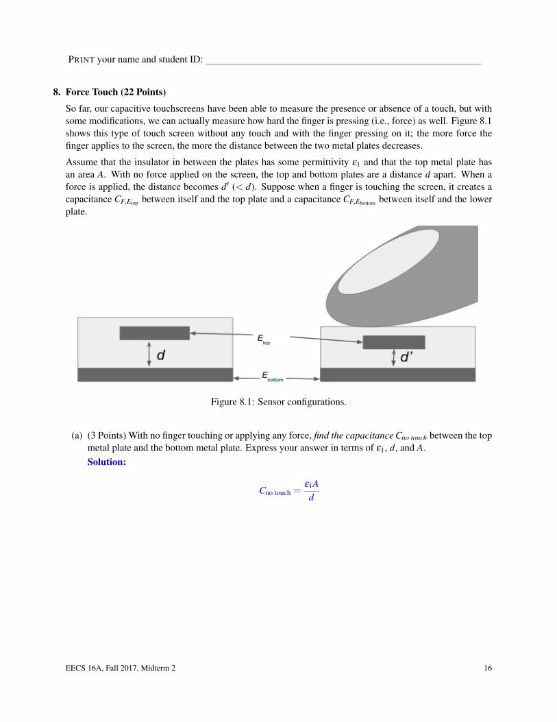
8. Force Touch (22 Points)
So far, our capacitive touchscreens have been able to measure the presence or absence of a touch, but withsome modifications, we can actually measure how hard the finger is pressing (i.e., force) as well. Figure 8.1shows this type of touch screen without any touch and with the finger pressing on it; the more force thefinger applies to the screen, the more the distance between the two metal plates decreases.
Assume that the insulator in between the plates has some permittivity ε1 and that the top metal plate hasan area A. With no force applied on the screen, the top and bottom plates are a distance d apart. When aforce is applied, the distance becomes d′ (< d). Suppose when a finger is touching the screen, it creates acapacitance CF,Etop between itself and the top plate and a capacitance CF,Ebottom between itself and the lowerplate.
Figure 8.1: Sensor configurations.
(a) (3 Points) With no finger touching or applying any force, find the capacitance Cno touch between the topmetal plate and the bottom metal plate. Express your answer in terms of ε1, d, and A.Solution:
Cno touch =ε1Ad
EECS 16A, Fall 2017, Midterm 2 16
PRINT your name and student ID:
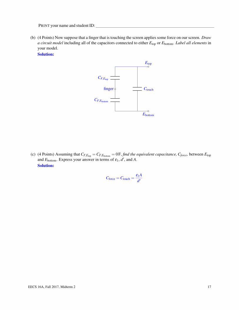
(b) (4 Points) Now suppose that a finger that is touching the screen applies some force on our screen. Drawa circuit model including all of the capacitors connected to either Etop or Ebottom. Label all elements inyour model.Solution:
CF,Etop
finger
CF,Ebottom
Ctouch
Etop
Ebottom
(c) (4 Points) Assuming that CF,Etop =CF,Ebottom = 0F, find the equivalent capacitance, Cforce, between Etopand Ebottom. Express your answer in terms of ε1, d′, and A.Solution:
Cforce =Ctouch =ε1Ad′
EECS 16A, Fall 2017, Midterm 2 17
PRINT your name and student ID:
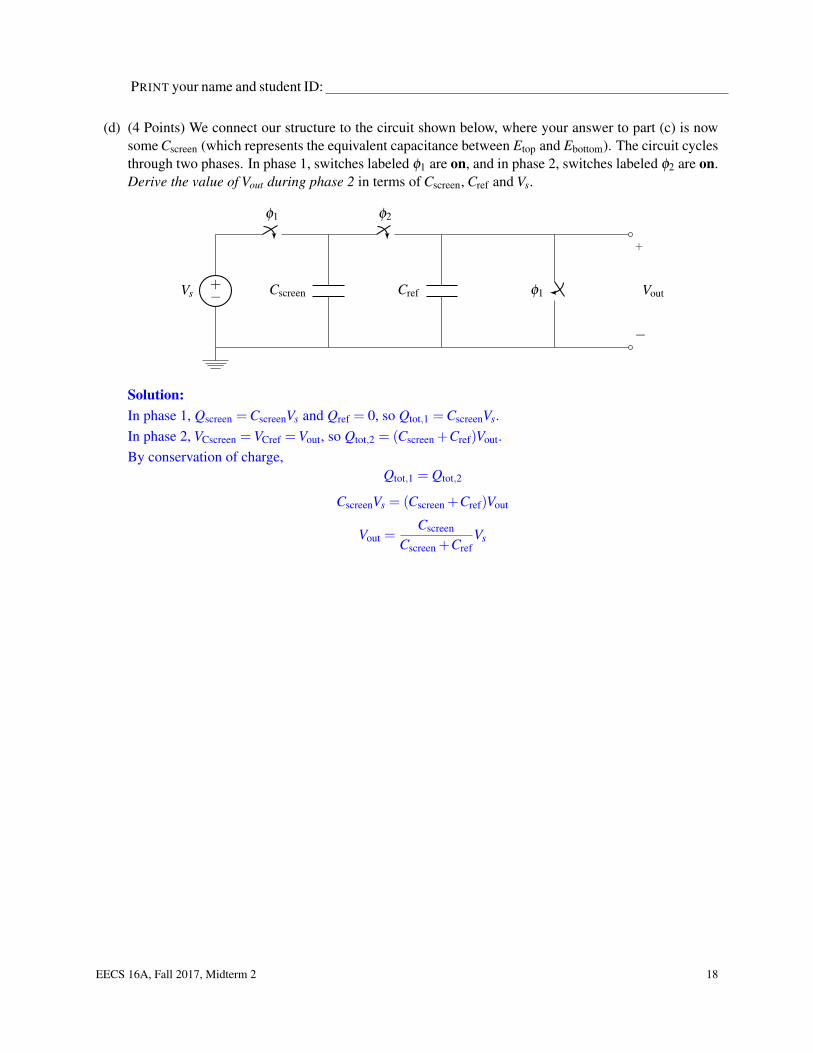
(d) (4 Points) We connect our structure to the circuit shown below, where your answer to part (c) is nowsome Cscreen (which represents the equivalent capacitance between Etop and Ebottom). The circuit cyclesthrough two phases. In phase 1, switches labeled φ1 are on, and in phase 2, switches labeled φ2 are on.Derive the value of Vout during phase 2 in terms of Cscreen, Cref and Vs.
−+Vs
φ1
Cscreen
φ2
Cref φ1
+
−
Vout
Solution:In phase 1, Qscreen =CscreenVs and Qref = 0, so Qtot,1 =CscreenVs.In phase 2, VCscreen =VCref =Vout, so Qtot,2 = (Cscreen +Cref)Vout.By conservation of charge,
Qtot,1 = Qtot,2
CscreenVs = (Cscreen +Cref)Vout
Vout =Cscreen
Cscreen +CrefVs
EECS 16A, Fall 2017, Midterm 2 18
PRINT your name and student ID:
(e) (7 Points) In the previous circuit, if the finger is pressing with a certain force F ′ and Vs = 5V, assumethat Vout = 2.5V during phase 2. We want to design a circuit that outputs 0V when we apply moreforce than F ′ and 3.3V when we apply less force than F ′.In the circuit below, label the terminals of the op-amp, indicate what you will connect its supplies to,and pick a value for Vref such that Vout,2 = 0V when more force than F ′ is applied and Vout,2 = 3.3Vwhen less force than F ′ is applied.
+
−
Vout
−+Vref
+
−
Vout,2
VDD
VSS
Solution:If more force than F ′ is applied, d′ decreases, so Cscreen increases, and Vout > 2.5V. Since we want tooutput 0V when we apply more force, we need the input terminal connected to the Vout to be labeled‘−’. We want to output 3.3V and 0V so VDD will be connected to 3.3V and VSS to 0V .
−
+
+
−
Vout
−+Vref 2.5V
+
−
Vout,2
VDD
3.3V
VSS
0V
EECS 16A, Fall 2017, Midterm 2 19
PRINT your name and student ID:
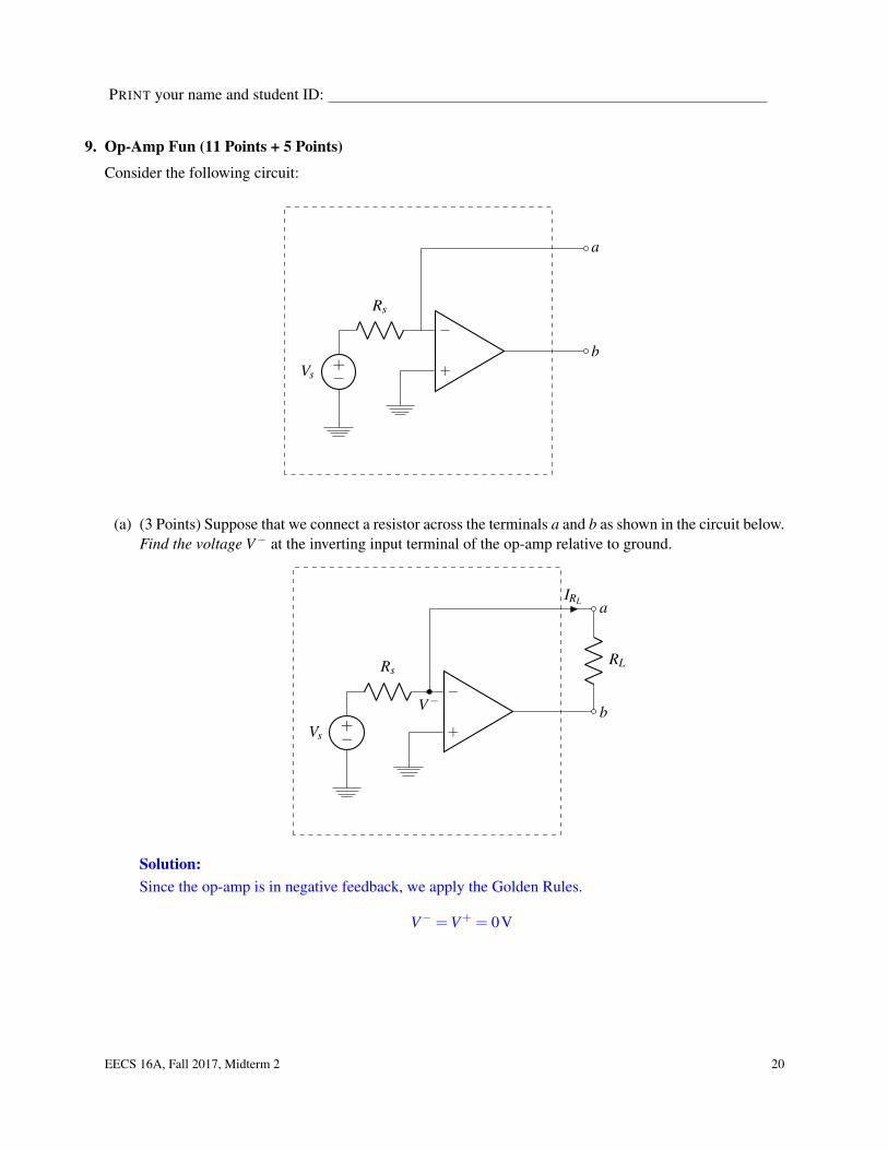
9. Op-Amp Fun (11 Points + 5 Points)
Consider the following circuit:
−
+
Rs
−+Vs
a
b
(a) (3 Points) Suppose that we connect a resistor across the terminals a and b as shown in the circuit below.Find the voltage V− at the inverting input terminal of the op-amp relative to ground.
−
+
Rs
−+Vs
V−
IRL a
RL
b
Solution:Since the op-amp is in negative feedback, we apply the Golden Rules.
V− =V+ = 0V
EECS 16A, Fall 2017, Midterm 2 20
PRINT your name and student ID:
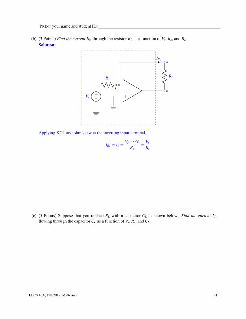
(b) (3 Points) Find the current IRL through the resistor RL as a function of Vs, Rs, and RL.Solution:
−
+
Rs
i1
−+Vs
IRL a
RL
b
Applying KCL and ohm’s law at the inverting input terminal,
IRL = i1 =Vs−0V
Rs=
Vs
Rs
(c) (5 Points) Suppose that you replace RL with a capacitor CL as shown below. Find the current ICL
flowing through the capacitor CL as a function of Vs, Rs, and CL.
EECS 16A, Fall 2017, Midterm 2 21
−
+
Rs
−+Vs
ICL a
CL
b
Solution:
−
+
Rs
−+Vs
ICL a
CL
+
−Vc
b
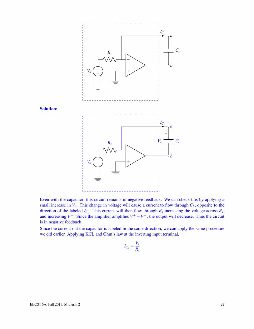
Even with the capacitor, this circuit remains in negative feedback. We can check this by applying asmall increase in Vb. This change in voltage will cause a current to flow through CL, opposite to thedirection of the labeled ICL . This current will then flow through Rs increasing the voltage across Rs,and increasing V−. Since the amplifier amplifies V+−V−, the output will decrease. Thus the circuitis in negative feedback.Since the current out the capacitor is labeled in the same direction, we can apply the same procedurewe did earlier. Applying KCL and Ohm’s law at the inverting input terminal,
ICL =Vs
Rs
EECS 16A, Fall 2017, Midterm 2 22
PRINT your name and student ID:
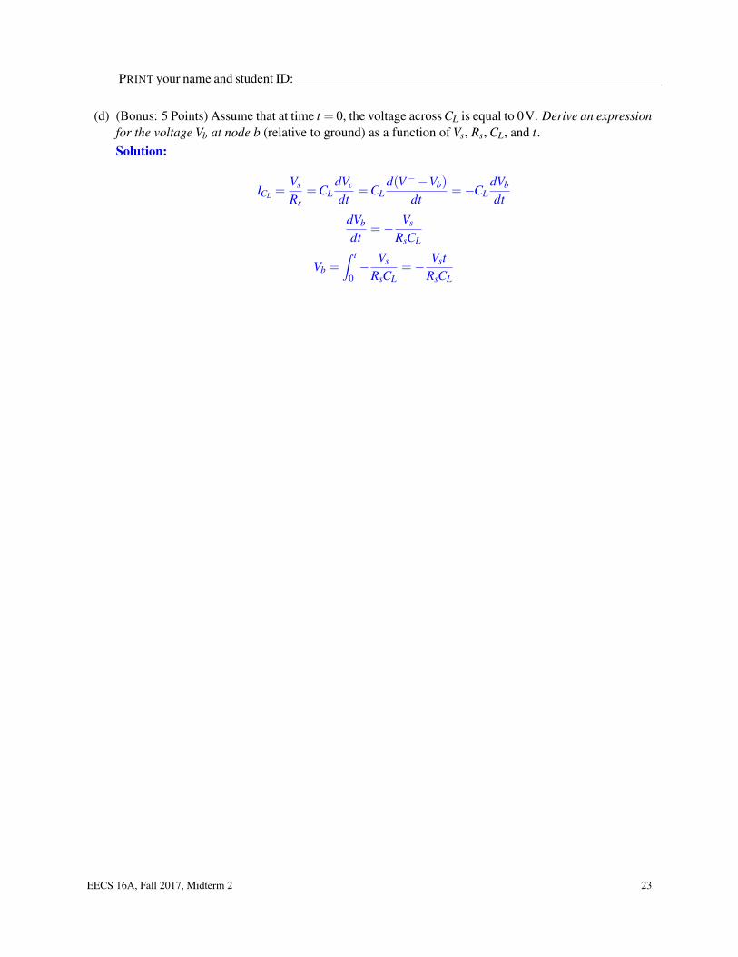
(d) (Bonus: 5 Points) Assume that at time t = 0, the voltage across CL is equal to 0V. Derive an expressionfor the voltage Vb at node b (relative to ground) as a function of Vs, Rs, CL, and t.Solution:
ICL =Vs
Rs=CL
dVc
dt=CL
d(V−−Vb)
dt=−CL
dVb
dt
dVb
dt=− Vs
RsCL
Vb =∫ t
0− Vs
RsCL=− Vst
RsCL
EECS 16A, Fall 2017, Midterm 2 23
PRINT your name and student ID:
10. Are You Resistive? (19 Points + 5 Points)
Bob is a quality control engineer, and his job is to document and analyze the test results of resistors madeby his company.
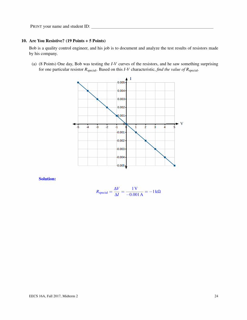
(a) (8 Points) One day, Bob was testing the I-V curves of the resistors, and he saw something surprisingfor one particular resistor Rspecial. Based on this I-V characteristic, find the value of Rspecial.
Solution:
Rspecial =∆V∆I
=1V
−0.001A=−1kΩ
EECS 16A, Fall 2017, Midterm 2 24
PRINT your name and student ID:
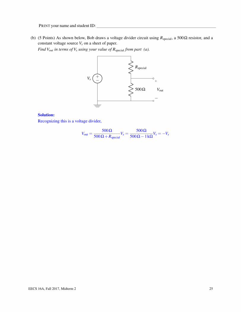
(b) (5 Points) As shown below, Bob draws a voltage divider circuit using Rspecial, a 500Ω resistor, and aconstant voltage source Vs on a sheet of paper.Find Vout in terms of Vs using your value of Rspecial from part (a).
−+Vs
Rspecial
500Ω
+
−
Vout
Solution:Recognizing this is a voltage divider,
Vout =500Ω
500Ω+RspecialVs =
500Ω
500Ω−1kΩVs =−Vs
EECS 16A, Fall 2017, Midterm 2 25
PRINT your name and student ID:
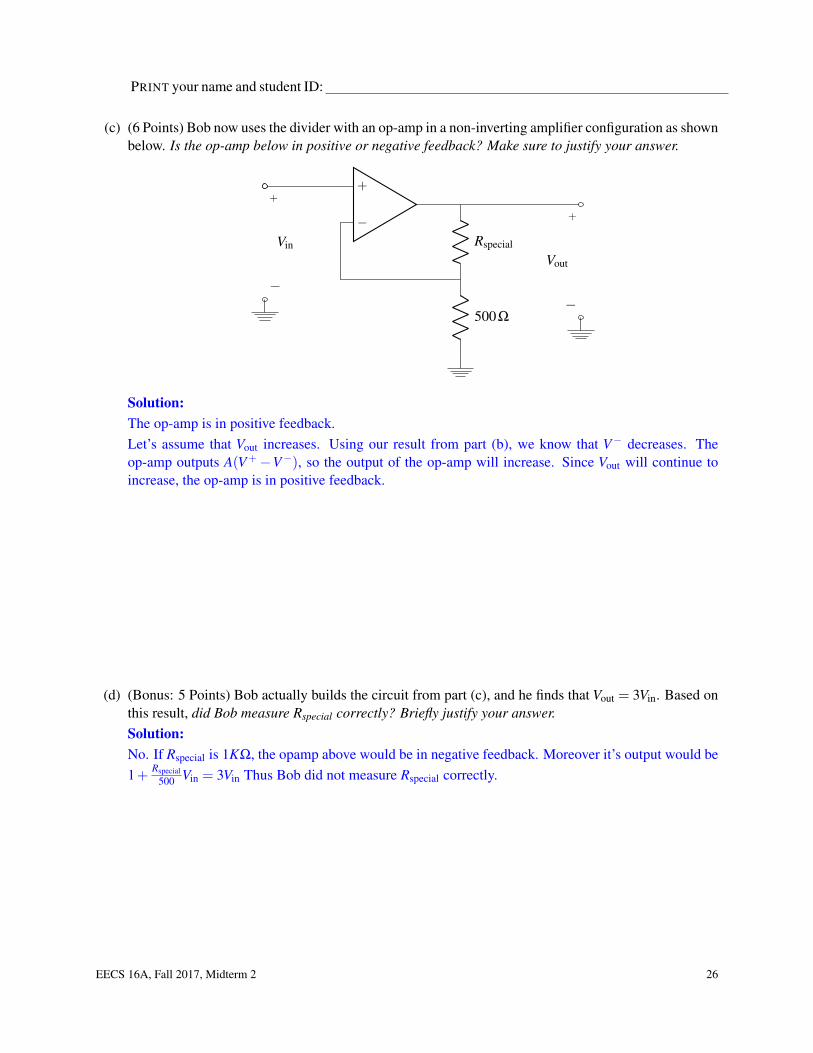
(c) (6 Points) Bob now uses the divider with an op-amp in a non-inverting amplifier configuration as shownbelow. Is the op-amp below in positive or negative feedback? Make sure to justify your answer.
−
+
Rspecial
500Ω
+
−
Vout
+
−
Vin
Solution:The op-amp is in positive feedback.Let’s assume that Vout increases. Using our result from part (b), we know that V− decreases. Theop-amp outputs A(V+−V−), so the output of the op-amp will increase. Since Vout will continue toincrease, the op-amp is in positive feedback.
(d) (Bonus: 5 Points) Bob actually builds the circuit from part (c), and he finds that Vout = 3Vin. Based onthis result, did Bob measure Rspecial correctly? Briefly justify your answer.Solution:No. If Rspecial is 1KΩ, the opamp above would be in negative feedback. Moreover it’s output would be1+ Rspecial
500 Vin = 3Vin Thus Bob did not measure Rspecial correctly.