34
Spring 2012 EECS150 - Lec11-sram2 Page EECS150 - Digital Design Lecture 11 - SRAM 2, Caches Feb 21, 2012 John Wawrzynek 1
Spring 2012 EECS150 - Lec11-sram2 Page
EECS150 - Digital DesignLecture 11 - SRAM 2, Caches
Feb 21, 2012John Wawrzynek
1

Spring 2012 EECS150 - Lec11-sram2 Page
Verilog Memory Synthesis Notes• Block RAMS and LUT RAMS all exist as primitive library elements
(similar to FDRSE) and can be instantiated. However, it is much more convenient to use inference.– Depending on how you write your verilog, you will get either a
collection of block RAMs, a collection of LUT RAMs, or a collection of flip-flops.
– The synthesizer uses size, and read style (synch versus asynch) to determine the best primitive type to use.
– It is possible to force mapping to a particular primitive by using synthesis directives. However, if you write your verilog correctly, you will not need to use directives.
– The synthesizer has limited capabilities (eg., it can combine primitives for more depth and width, but is limited on porting options). Be careful, as you might not get what you want.
• Check out “CoreGen” as an alternative. Creates a custom module for instantiation from a GUI.
2

Spring 2012 EECS150 - Lec11-sram2 Page
Inferring RAMs in Verilog
3
// 64X1 RAM implementation using distributed RAM
module ram64X1 (clk, we, d, addr, q);input clk, we, d;input [5:0] addr;output q;
reg [63:0] temp; always @ (posedge clk)
if(we) temp[addr] <= d;
assign q = temp[addr];
endmodule
Asynchronous read infers LUT RAM
Verilog reg array used with “always @ (posedge ... infers
memory array.

Spring 2012 EECS150 - Lec11-sram2 Page
Dual-read-port LUT RAM
4
// // Multiple-Port RAM Descriptions // module v_rams_17 (clk, we, wa, ra1, ra2, di, do1, do2); input clk; input we; input [5:0] wa; input [5:0] ra1; input [5:0] ra2; input [15:0] di; output [15:0] do1; output [15:0] do2; reg [15:0] ram [63:0]; always @(posedge clk) begin if (we) ram[wa] <= di; end assign do1 = ram[ra1]; assign do2 = ram[ra2]; endmodule
Multiple reference to same array.
Spring 2012 EECS150 - Lec11-sram2 Page
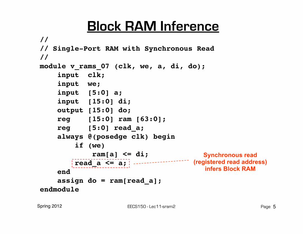
Block RAM Inference
5
// // Single-Port RAM with Synchronous Read // module v_rams_07 (clk, we, a, di, do); input clk; input we; input [5:0] a; input [15:0] di; output [15:0] do; reg [15:0] ram [63:0]; reg [5:0] read_a; always @(posedge clk) begin if (we) ram[a] <= di; read_a <= a; end assign do = ram[read_a]; endmodule
Synchronous read (registered read address)
infers Block RAM

Spring 2012 EECS150 - Lec11-sram2 Page
Block RAM initialization
6
module RAMB4_S4 (data_out, ADDR, data_in, CLK, WE); output[3:0] data_out; input [2:0] ADDR; input [3:0] data_in; input CLK, WE; reg [3:0] mem [7:0]; reg [3:0] read_addr;
initial begin $readmemb("data.dat", mem); end always@(posedge CLK) read_addr <= ADDR;
assign data_out = mem[read_addr];
always @(posedge CLK) if (WE) mem[ADDR] = data_in;
endmodule
“data.dat” contains initial RAM contents, it gets put into the bitfile and loaded at configuration time. (Remake bits to change contents)
Spring 2012 EECS150 - Lec11-sram2 Page
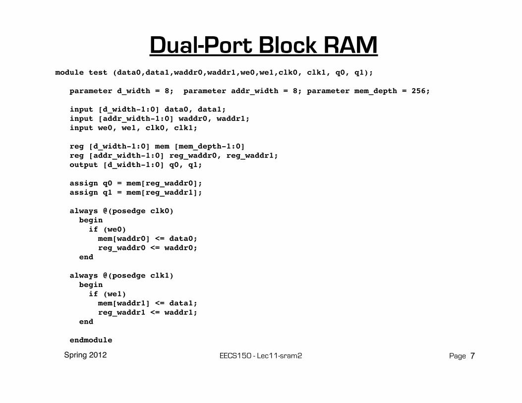
Dual-Port Block RAM
7
module test (data0,data1,waddr0,waddr1,we0,we1,clk0, clk1, q0, q1);
parameter d_width = 8; parameter addr_width = 8; parameter mem_depth = 256;
input [d_width-1:0] data0, data1; input [addr_width-1:0] waddr0, waddr1; input we0, we1, clk0, clk1;
reg [d_width-1:0] mem [mem_depth-1:0] reg [addr_width-1:0] reg_waddr0, reg_waddr1; output [d_width-1:0] q0, q1;
assign q0 = mem[reg_waddr0]; assign q1 = mem[reg_waddr1];
always @(posedge clk0) begin if (we0) mem[waddr0] <= data0; reg_waddr0 <= waddr0; end
always @(posedge clk1) begin if (we1) mem[waddr1] <= data1; reg_waddr1 <= waddr1; end
endmodule

Spring 2012 EECS150 - Lec11-sram2 Page
First-in-first-out (FIFO) Memory• Used to implement queues. • These find common use in
computers and communication circuits.
• Generally, used to “decouple” actions of producer and consumer:
• Producer can perform many writes without consumer performing any reads (or vis versa). However, because of finite buffer size, on average, need equal number of reads and writes.
• Typical uses: – interfacing I/O devices.
Example network interface. Data bursts from network, then processor bursts to memory buffer (or reads one word at a time from interface). Operations not synchronized.
– Example: Audio output. Processor produces output samples in bursts (during process swap-in time). Audio DAC clocks it out at constant sample rate.
stating state
after write
after read
abc
abcd
bcd
8

Spring 2012 EECS150 - Lec11-sram2 Page
FIFO Interfaces
• After write or read operation, FULL and EMPTY indicate status of buffer.
• Used by external logic to control own reading from or writing to the buffer.
• FIFO resets to EMPTY state.• HALF FULL (or other indicator of
partial fullness) is optional.
• Address pointers are used internally to keep next write position and next read position into a dual-port memory.
• If pointers equal after write ⇒ FULL:
• If pointers equal after read ⇒ EMPTY:
DIN
DOUT
WE
REEMPTY
FULLHALF FULL
RST CLK
FIFOwrite ptr
read ptr
write ptr read ptr
write ptr read ptr
9
Spring 2012 EECS150 - Lec11-sram2 Page
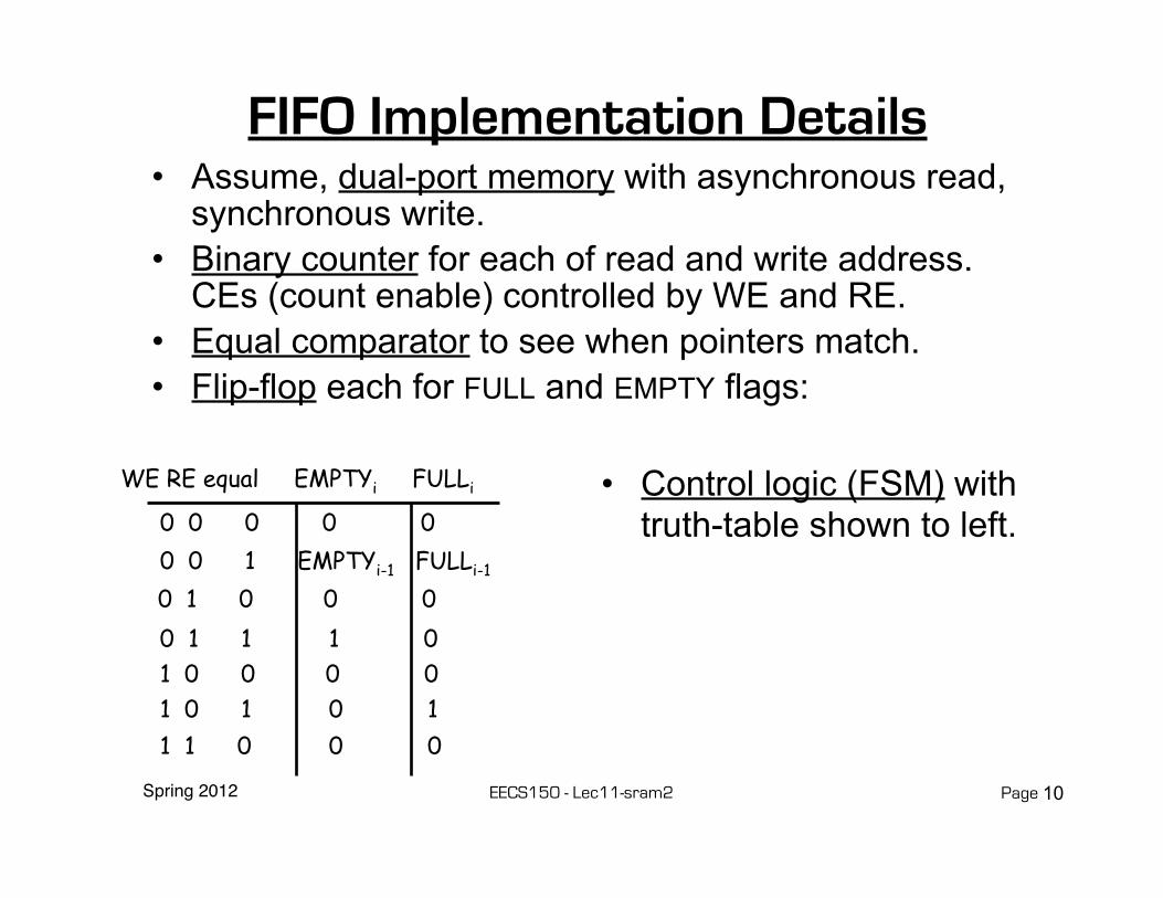
FIFO Implementation Details
WE RE equal EMPTYi FULLi
0 0 0 0 0 0 0 1 EMPTYi-1 FULLi-1
0 1 0 0 0 0 1 1 1 0 1 0 0 0 0 1 0 1 0 1 1 1 0 0 0
• Assume, dual-port memory with asynchronous read, synchronous write.
• Binary counter for each of read and write address. CEs (count enable) controlled by WE and RE.
• Equal comparator to see when pointers match.• Flip-flop each for FULL and EMPTY flags: • Control logic (FSM) with
truth-table shown to left.
10
Spring 2012 EECS150 - Lec11-sram2 Page
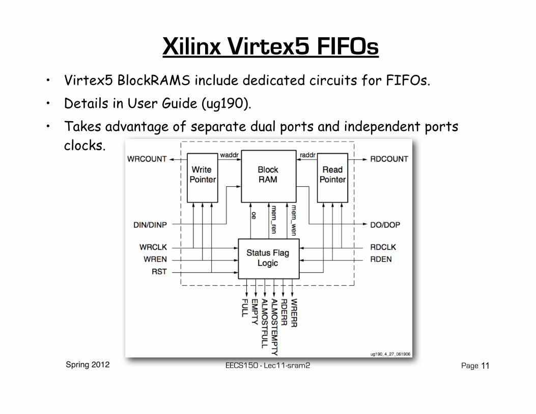
Xilinx Virtex5 FIFOs• Virtex5 BlockRAMS include dedicated circuits for FIFOs.• Details in User Guide (ug190).• Takes advantage of separate dual ports and independent ports
clocks.
11

Spring 2012 EECS150 - Lec11-sram2 Page
Processor Design Considerations (1/2)• Register File: Consider distributed RAM (LUT RAM)
– Size is close to what is needed: distributed RAM primitive configurations are 32 or 64 bits deep. Extra width is easily achieved by parallel arrangements.
– LUT-RAM configurations offer multi-porting options - useful for register files.
– Asynchronous read, might be useful by providing flexibility on where to put register read in the pipeline.
• Instruction / Data Caches : Consider Block RAM– Higher density, lower cost for large number of bits– A single 36kbit Block RAM implements 1K 32-bit words.– Configuration stream based initialization, permits a simple “boot
strap” procedure.• Other Memories in Project? Video?• Main memory will be in external DRAM
12

Spring 2012 EECS150 - Lec11-sram2 Page
XUP Board External SRAM
13
More generally, how does software interface to I/O devices?
*ZBT (ZBT stands for zero bus turnaround) — the turnaround is the number of clock cycles it takes to change access to the SRAM from write to read and vice versa. The turnaround for ZBT SRAMs or the latency between read and write cycle is zero.
“ZBT” synchronous SRAM, 9 Mb on 32-bit data bus, with four “parity” bits256K x 36 bits(located under the removable LCD)

Spring 2012 EECS150 - Lec11-sram2 Page
XUP Board External DRAM
14
More generally, how does software interface to I/O devices?
*SO-DIMM stands for small outline dual in-line memory module. SO-DIMMS are often used in systems which have space restrictions such as notebooks.*DDR2 stands for second generation double data rate. DDR transfers data both on the rising and falling edges of the clock signal.
256 MByte DDR2 DRAM with 400MHz data rate.
Spring 2012 EECS150 - Lec11-sram2 Page
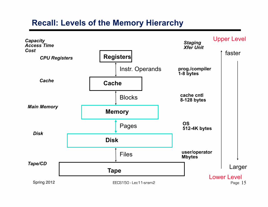
Recall: Levels of the Memory Hierarchy
CPU Registers
Cache
Main Memory
Disk
CapacityAccess TimeCost
Tape/CD
Registers
Cache
Memory
Disk
Tape
Instr. Operands
Blocks
Pages
Files
StagingXfer Unit
prog./compiler1-8 bytes
cache cntl8-128 bytes
OS512-4K bytes
user/operatorMbytes
Upper Level
Lower Level
faster
Larger
15
Spring 2012 EECS150 - Lec11-sram2 Page
Review from 61C
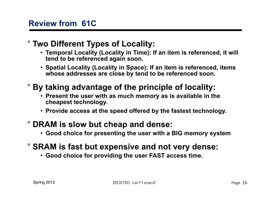
° Two Different Types of Locality:• Temporal Locality (Locality in Time): If an item is referenced, it will
tend to be referenced again soon.• Spatial Locality (Locality in Space): If an item is referenced, items
whose addresses are close by tend to be referenced soon.
° By taking advantage of the principle of locality:• Present the user with as much memory as is available in the
cheapest technology.• Provide access at the speed offered by the fastest technology.
° DRAM is slow but cheap and dense:• Good choice for presenting the user with a BIG memory system
° SRAM is fast but expensive and not very dense:• Good choice for providing the user FAST access time.
16

Spring 2012 EECS150 - Lec11-sram2 Page
Example: 1 KB Direct Mapped Cache with 32 B Blocks
° For a 2N byte cache:• The uppermost (32 - N) bits are always the Cache Tag• The lowest M bits are the Byte Select (Block Size = 2M)
Cache Index
0123
:
Cache DataByte 0
0431
:
Cache Tag Example: 0x50Ex: 0x01
0x50
Stored as partof the cache “state”
Valid Bit
:31
Byte 1Byte 31 :
Byte 32Byte 33Byte 63 :Byte 992Byte 1023 :
Cache Tag
Byte SelectEx: 0x00
9Block address
17

Spring 2012 EECS150 - Lec11-sram2 Page
Block Size Tradeoff
° In general, larger block size take advantage of spatial locality BUT:
• Larger block size means larger miss penalty:- Takes longer time to fill up the block
• If block size is too big relative to cache size, miss rate will go up- Too few cache blocks
° In general, Average Access Time: = Hit Time x (1 - Miss Rate) + Miss Penalty x Miss Rate
MissPenalty
Block Size
MissRate Exploits Spatial Locality
Fewer blocks: compromisestemporal locality
AverageAccess
Time
Increased Miss Penalty& Miss Rate
Block Size Block Size18

Spring 2012 EECS150 - Lec11-sram2 Page
Extreme Example: single line
° Cache Size = 4 bytes Block Size = 4 bytes
• Only ONE entry in the cache
° If an item is accessed, likely that it will be accessed again soon
• But it is unlikely that it will be accessed again immediately!!!• The next access will likely to be a miss again
- Continually loading data into the cache butdiscard (force out) them before they are used again
- Worst nightmare of a cache designer: Ping Pong Effect
° Conflict Misses are misses caused by:• Different memory locations mapped to the same cache index
- Solution 1: make the cache size bigger - Solution 2: Multiple entries for the same Cache Index
0 Cache DataValid Bit
Byte 0Byte 1Byte 3 Cache Tag
Byte 2
19
Spring 2012 EECS150 - Lec11-sram2 Page
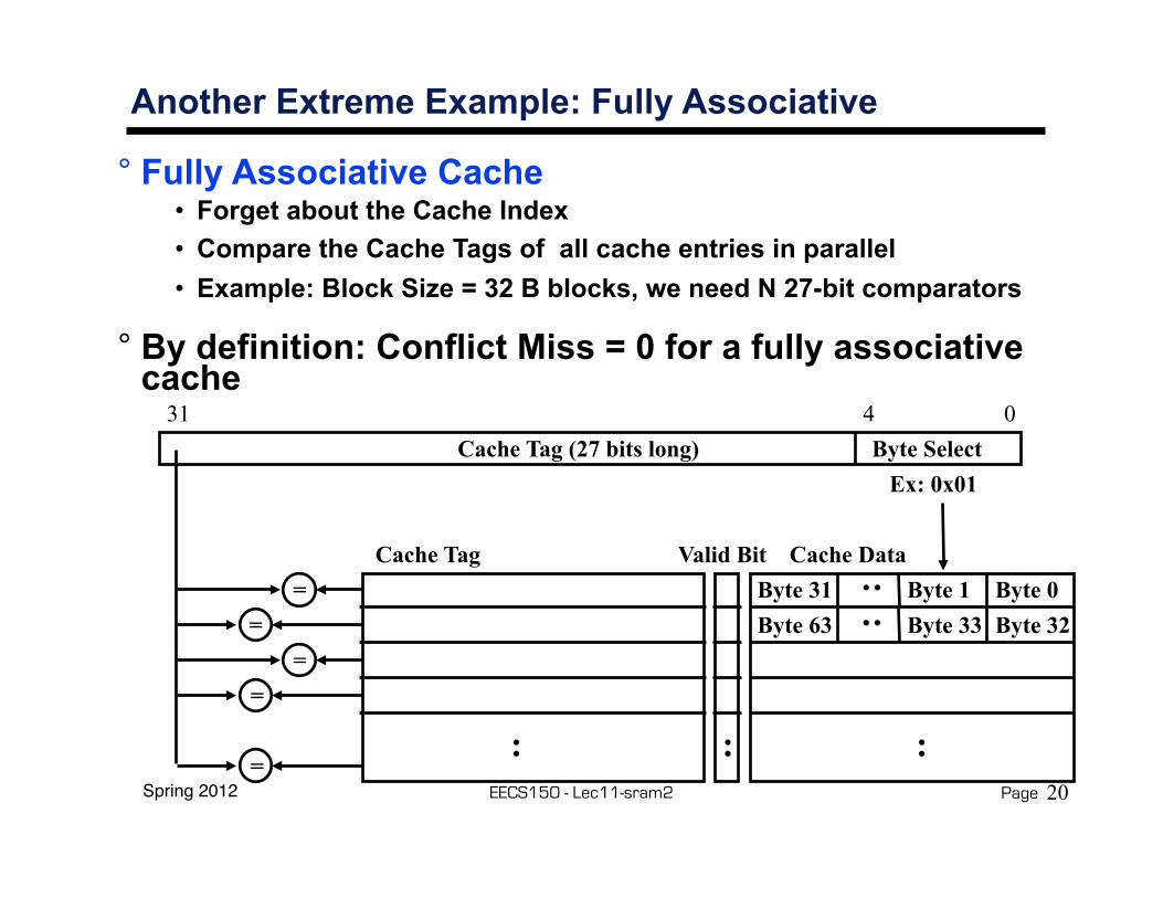
Another Extreme Example: Fully Associative
° Fully Associative Cache• Forget about the Cache Index• Compare the Cache Tags of all cache entries in parallel• Example: Block Size = 32 B blocks, we need N 27-bit comparators
° By definition: Conflict Miss = 0 for a fully associative cache
:
Cache DataByte 0
0431
:
Cache Tag (27 bits long)
Valid Bit
:
Byte 1Byte 31 :
Byte 32Byte 33Byte 63 :
Cache Tag
Byte SelectEx: 0x01
=
==
=
=20
Spring 2012 EECS150 - Lec11-sram2 Page
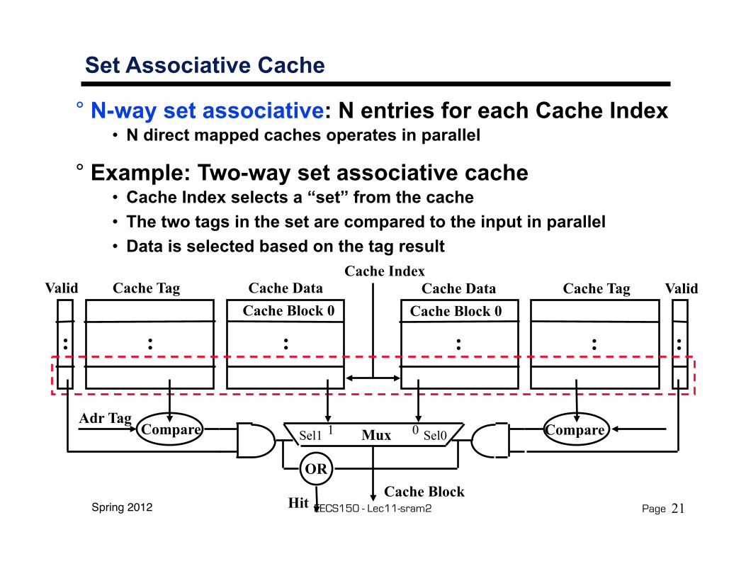
Set Associative Cache
° N-way set associative: N entries for each Cache Index• N direct mapped caches operates in parallel
° Example: Two-way set associative cache• Cache Index selects a “set” from the cache• The two tags in the set are compared to the input in parallel• Data is selected based on the tag result
Cache DataCache Block 0
Cache TagValid
:: :
Cache DataCache Block 0
Cache Tag Valid
: ::
Cache Index
Mux 01Sel1 Sel0
Cache Block
CompareAdr Tag
Compare
OR
Hit 21

Spring 2012 EECS150 - Lec11-sram2 Page
Disadvantage of Set Associative Cache
° N-way Set Associative Cache versus Direct Mapped Cache:
• N comparators vs. 1• Extra MUX delay for the data• Data comes AFTER Hit/Miss decision and set selection
° In a direct mapped cache, Cache Block is available BEFORE Hit/Miss:
• Possible to assume a hit and continue. Recover later if miss.
Cache DataCache Block 0
Cache Tag Valid
: ::
Cache DataCache Block 0
Cache TagValid
:: :
Cache Index
Mux 01Sel1 Sel0
Cache Block
CompareAdr Tag
Compare
OR
Hit22
Spring 2012 EECS150 - Lec11-sram2 Page
A Summary on Sources of Cache Misses
° Compulsory (cold start or process migration, first reference): first access to a block
• “Cold” fact of life: not a whole lot you can do about it• Note: If you are going to run “billions” of instruction,
Compulsory Misses are insignificant
° Conflict (collision):• Multiple memory locations mapped
to the same cache location• Solution 1: increase cache size• Solution 2: increase associativity
° Capacity:• Cache cannot contain all blocks access by the program• Solution: increase cache size
° Invalidation: other process (e.g., I/O) updates memory
23
Spring 2012 EECS150 - Lec11-sram2 Page
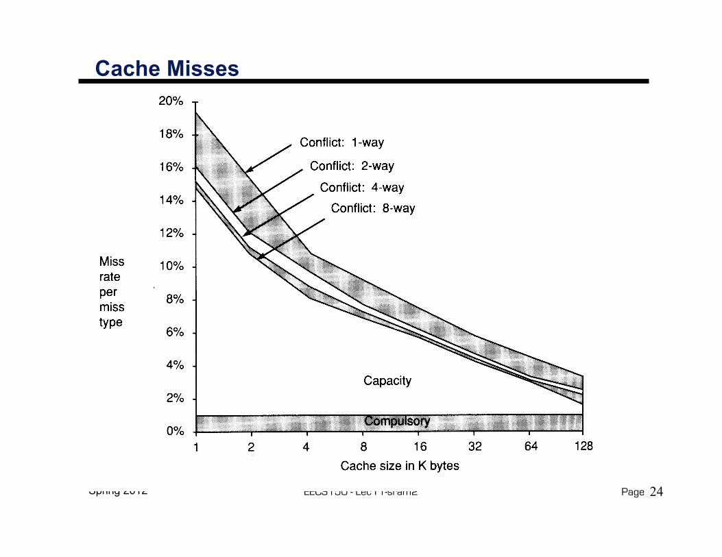
Cache Misses
24
Spring 2012 EECS150 - Lec11-sram2 Page
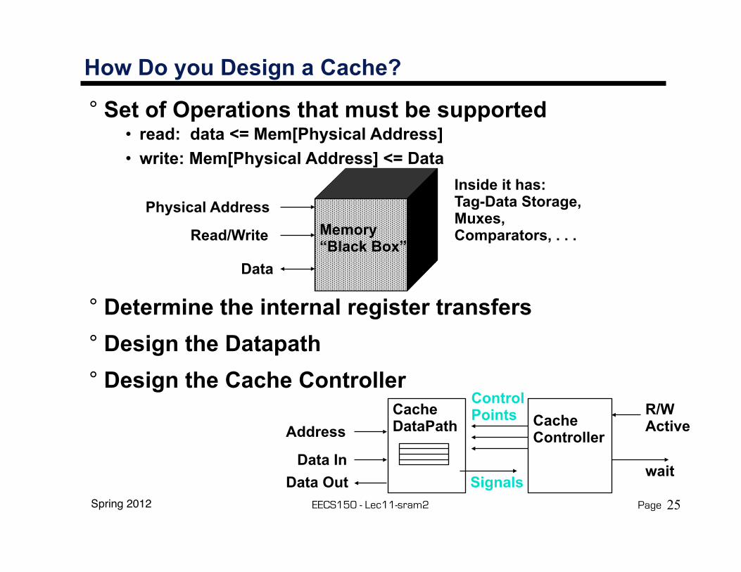
How Do you Design a Cache?
° Set of Operations that must be supported• read: data <= Mem[Physical Address]• write: Mem[Physical Address] <= Data
° Determine the internal register transfers° Design the Datapath° Design the Cache Controller
Physical Address
Read/Write
Data
Memory“Black Box”
Inside it has:Tag-Data Storage,Muxes,Comparators, . . .
CacheController
CacheDataPathAddress
Data InData Out
R/WActive
ControlPoints
Signalswait
25
Spring 2012 EECS150 - Lec11-sram2 Page
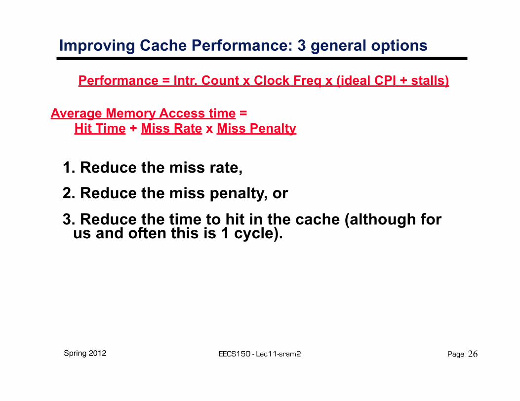
Improving Cache Performance: 3 general options
1. Reduce the miss rate, 2. Reduce the miss penalty, or3. Reduce the time to hit in the cache (although for
us and often this is 1 cycle).
Performance = Intr. Count x Clock Freq x (ideal CPI + stalls)
Average Memory Access time = Hit Time + Miss Rate x Miss Penalty
26
Spring 2012 EECS150 - Lec11-sram2 Page
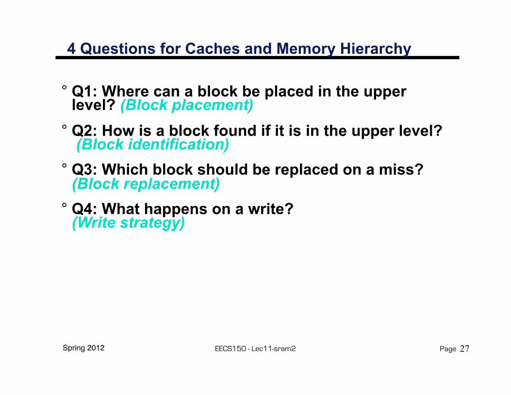
4 Questions for Caches and Memory Hierarchy
° Q1: Where can a block be placed in the upper level? (Block placement)
° Q2: How is a block found if it is in the upper level? (Block identification)
° Q3: Which block should be replaced on a miss? (Block replacement)
° Q4: What happens on a write? (Write strategy)
27
Spring 2012 EECS150 - Lec11-sram2 Page
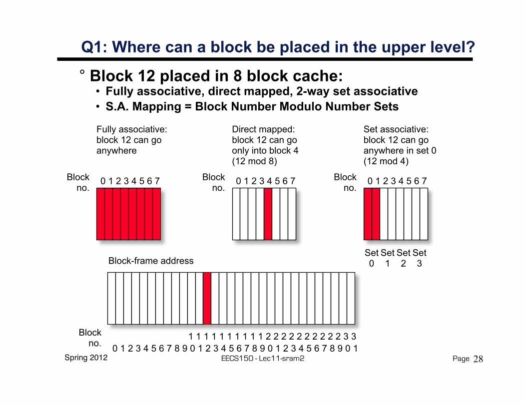
Q1: Where can a block be placed in the upper level?
° Block 12 placed in 8 block cache:• Fully associative, direct mapped, 2-way set associative• S.A. Mapping = Block Number Modulo Number Sets
0 1 2 3 4 5 6 7Blockno.
Fully associative:block 12 can go anywhere
0 1 2 3 4 5 6 7Blockno.
Direct mapped:block 12 can go only into block 4 (12 mod 8)
0 1 2 3 4 5 6 7Blockno.
Set associative:block 12 can go anywhere in set 0 (12 mod 4)
Set0
Set1
Set2
Set3
0 1 2 3 4 5 6 7 8 9 0 1 2 3 4 5 6 7 8 9 0 1 2 3 4 5 6 7 8 9 0 1
Block-frame address
1 1 1 1 1 1 1 1 1 1 2 2 2 2 2 2 2 2 2 2 3 3Blockno.
28

Spring 2012 EECS150 - Lec11-sram2 Page
Q2: How is a block found if it is in the upper level?
° Direct indexing (using index and block offset), tag compares, or combination
° Increasing associativity shrinks index, expands tag
Blockoffset
Block AddressTag Index
29
Spring 2012 EECS150 - Lec11-sram2 Page
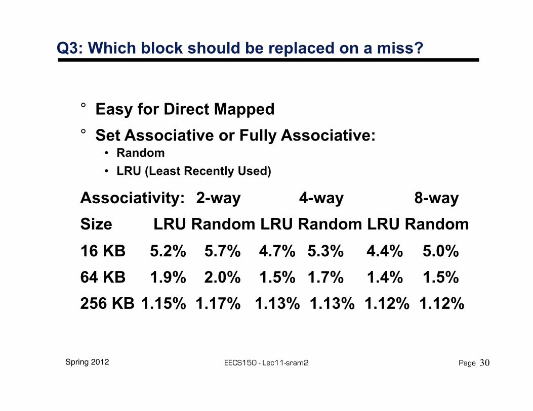
Q3: Which block should be replaced on a miss?
° Easy for Direct Mapped° Set Associative or Fully Associative:
• Random• LRU (Least Recently Used)
Associativity: 2-way 4-way 8-waySize LRU Random LRU Random LRU Random16 KB 5.2% 5.7% 4.7% 5.3% 4.4% 5.0%64 KB 1.9% 2.0% 1.5% 1.7% 1.4% 1.5%256 KB 1.15% 1.17% 1.13% 1.13% 1.12% 1.12%
30
Spring 2012 EECS150 - Lec11-sram2 Page
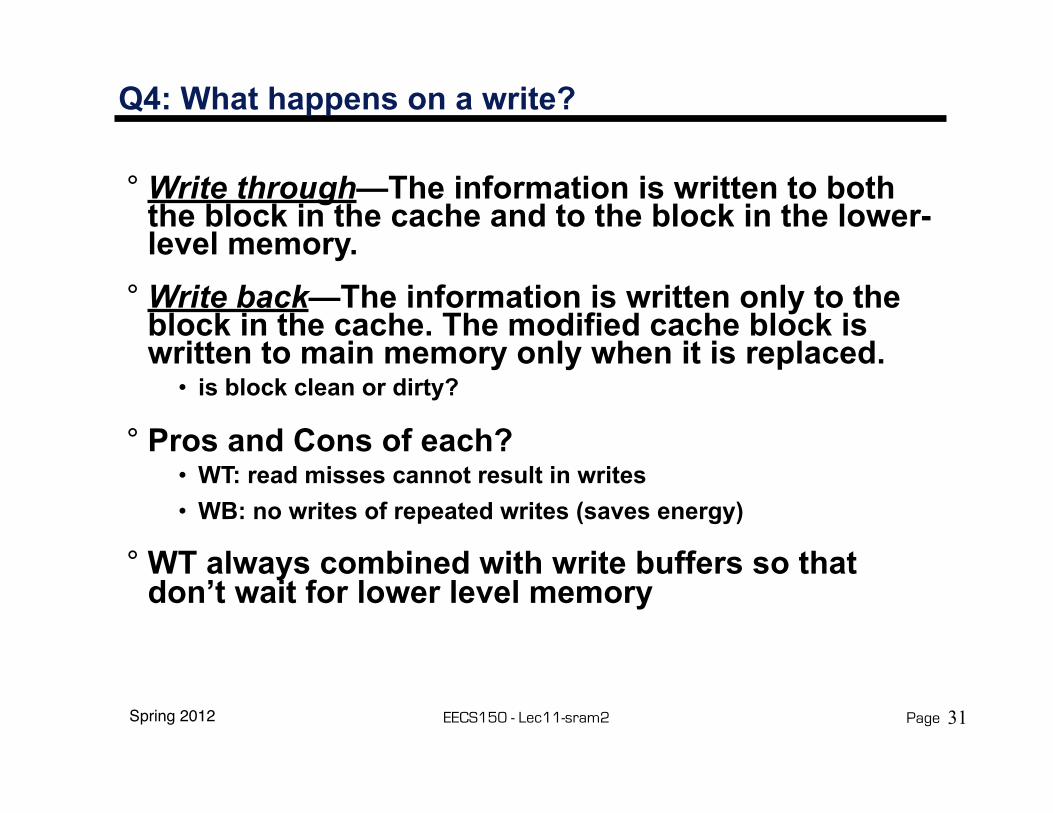
Q4: What happens on a write?
° Write through—The information is written to both the block in the cache and to the block in the lower-level memory.
° Write back—The information is written only to the block in the cache. The modified cache block is written to main memory only when it is replaced.
• is block clean or dirty?
° Pros and Cons of each?• WT: read misses cannot result in writes• WB: no writes of repeated writes (saves energy)
° WT always combined with write buffers so that don’t wait for lower level memory
31
Spring 2012 EECS150 - Lec11-sram2 Page
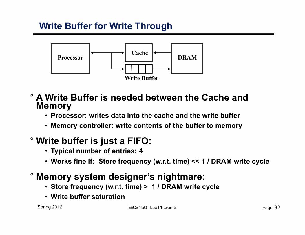
Write Buffer for Write Through
° A Write Buffer is needed between the Cache and Memory
• Processor: writes data into the cache and the write buffer• Memory controller: write contents of the buffer to memory
° Write buffer is just a FIFO:• Typical number of entries: 4• Works fine if: Store frequency (w.r.t. time) << 1 / DRAM write cycle
° Memory system designer’s nightmare:• Store frequency (w.r.t. time) > 1 / DRAM write cycle• Write buffer saturation
ProcessorCache
Write Buffer
DRAM
32
Spring 2012 EECS150 - Lec11-sram2 Page
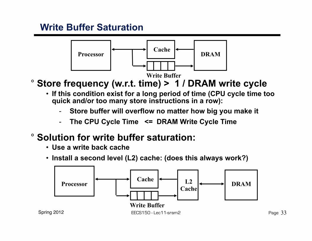
Write Buffer Saturation
° Store frequency (w.r.t. time) > 1 / DRAM write cycle• If this condition exist for a long period of time (CPU cycle time too
quick and/or too many store instructions in a row):- Store buffer will overflow no matter how big you make it- The CPU Cycle Time <= DRAM Write Cycle Time
° Solution for write buffer saturation:• Use a write back cache• Install a second level (L2) cache: (does this always work?)
ProcessorCache
Write Buffer
DRAM
ProcessorCache
Write Buffer
DRAML2Cache
33

Spring 2012 EECS150 - Lec11-sram2 Page
Write-miss Policy: Write Allocate versus Not Allocate
° Assume: a 16-bit write to memory location 0x0 and causes a miss
• Do we read in the block?- Yes: Write Allocate- No: Write Not Allocate
Cache Index
0123
:
Cache DataByte 0
0431
:
Cache Tag Example: 0x00Ex: 0x00
0x50Valid Bit
:31
Byte 1Byte 31 :
Byte 32Byte 33Byte 63 :Byte 992Byte 1023 :
Cache Tag
Byte SelectEx: 0x00
9
34


