NREL is a national laboratory of the U.S. Department of Energy, Office of Energy Efficiency and Renewable Energy, operated by the Alliance for Sustainable Energy, LLC. EERE QC Workshop: Overview of Quality Control Techniques Michael Ulsh, NREL December 9, 2013
Transcript
NREL is a national laboratory of the U.S. Department of Energy, Office of Energy Efficiency and Renewable Energy, operated by the Alliance for Sustainable Energy, LLC.
EERE QC Workshop: Overview of Quality Control Techniques
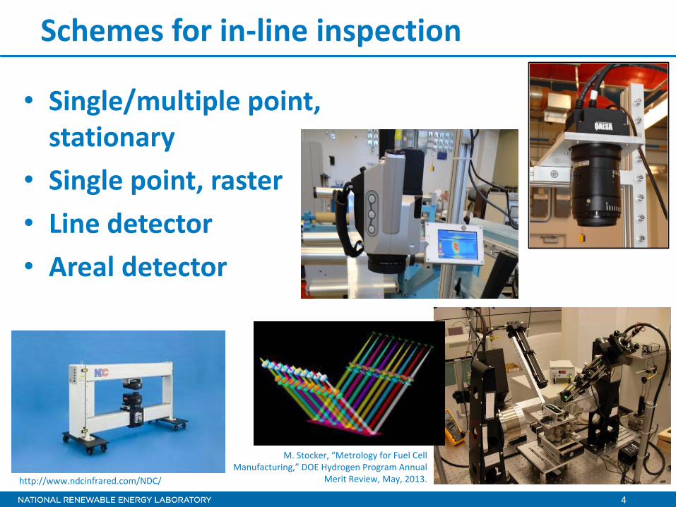
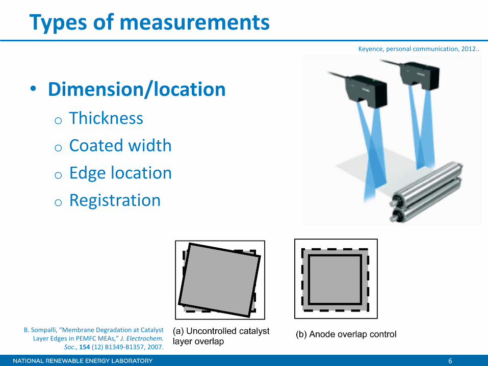
• Dimension/location o Thickness o Coated width o Edge location o Registration
Keyence, personal communication, 2012..
B. Sompalli, “Membrane Degradation at Catalyst Layer Edges in PEMFC MEAs,” J. Electrochem.
Soc., 154 (12) B1349-B1357, 2007.
7
Types of measurements
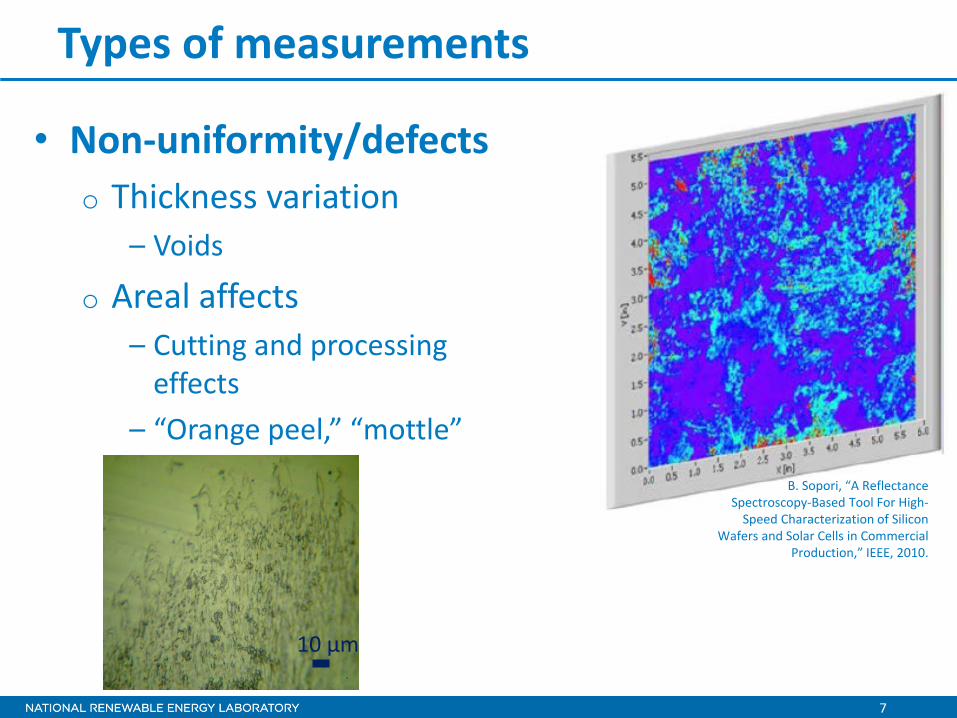
• Non-uniformity/defects o Thickness variation
– Voids
o Areal affects – Cutting and processing
effects – “Orange peel,” “mottle”
10 µm
B. Sopori, “A Reflectance Spectroscopy-Based Tool For High-
Speed Characterization of Silicon Wafers and Solar Cells in Commercial
Production,” IEEE, 2010.
8
Types of measurements
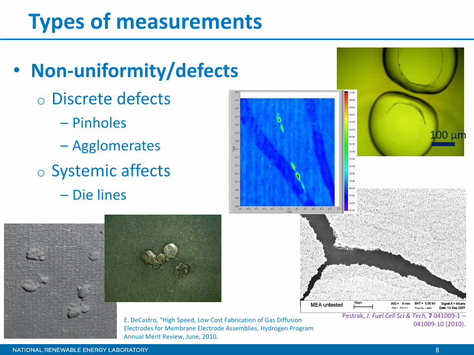
• Non-uniformity/defects o Discrete defects
– Pinholes – Agglomerates
o Systemic affects – Die lines
100 µm
E. DeCastro, “High Speed, Low Cost Fabrication of Gas Diffusion Electrodes for Membrane Electrode Assemblies, Hydrogen Program Annual Merit Review, June, 2010.
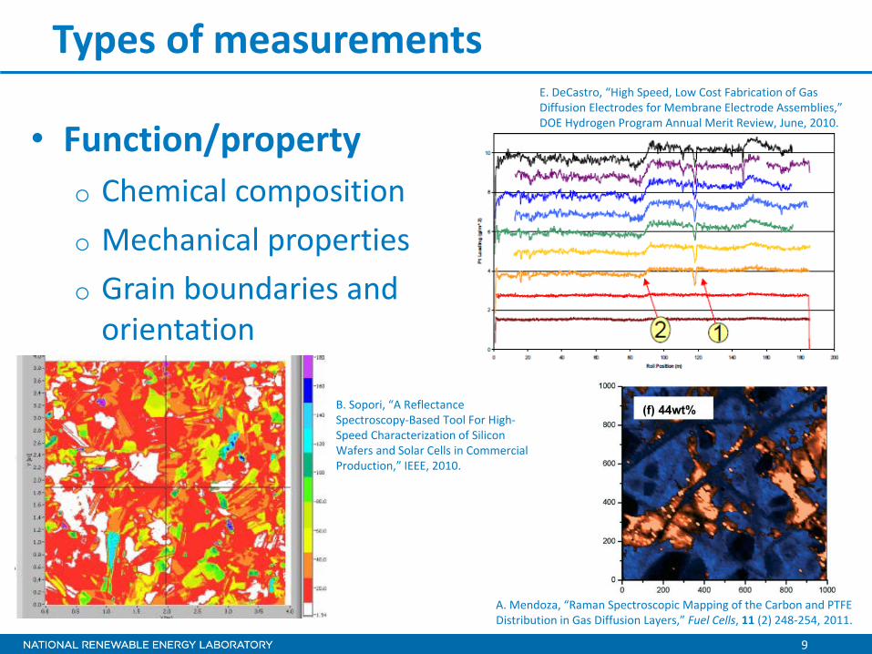
• Function/property o Chemical composition o Mechanical properties o Grain boundaries and
orientation
A. Mendoza, “Raman Spectroscopic Mapping of the Carbon and PTFE Distribution in Gas Diffusion Layers,” Fuel Cells, 11 (2) 248-254, 2011.
E. DeCastro, “High Speed, Low Cost Fabrication of Gas Diffusion Electrodes for Membrane Electrode Assemblies,” DOE Hydrogen Program Annual Merit Review, June, 2010.
B. Sopori, “A Reflectance Spectroscopy-Based Tool For High-Speed Characterization of Silicon Wafers and Solar Cells in Commercial Production,” IEEE, 2010.
10
Types of measurements
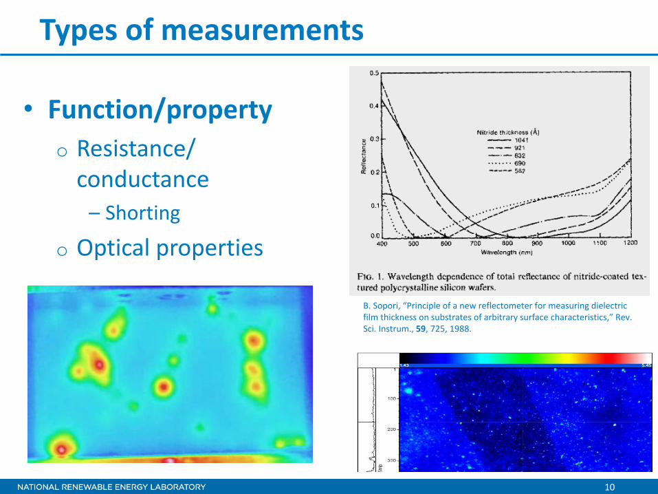
• Function/property o Resistance/
conductance – Shorting
o Optical properties
B. Sopori, “Principle of a new reflectometer for measuring dielectric film thickness on substrates of arbitrary surface characteristics,” Rev. Sci. Instrum., 59, 725, 1988.
11
Point measurements
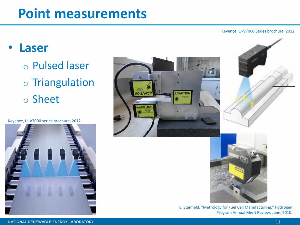
• Laser o Pulsed laser o Triangulation o Sheet
E. Stanfield, “Metrology for Fuel Cell Manufacturing,” Hydrogen Program Annual Merit Review, June, 2010.
Keyence, LJ-V7000 Series brochure, 2012.
Keyence, LJ-V7000 series brochure, 2012.
12
Point measurements
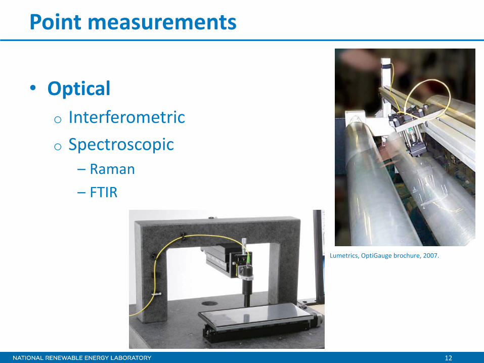
• Optical o Interferometric o Spectroscopic
– Raman – FTIR
Lumetrics, OptiGauge brochure, 2007.
13
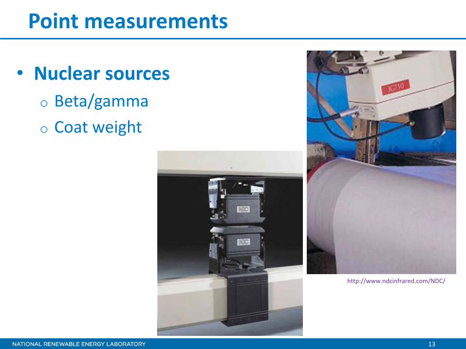
Point measurements
• Nuclear sources o Beta/gamma o Coat weight
http://www.ndcinfrared.com/NDC/
14
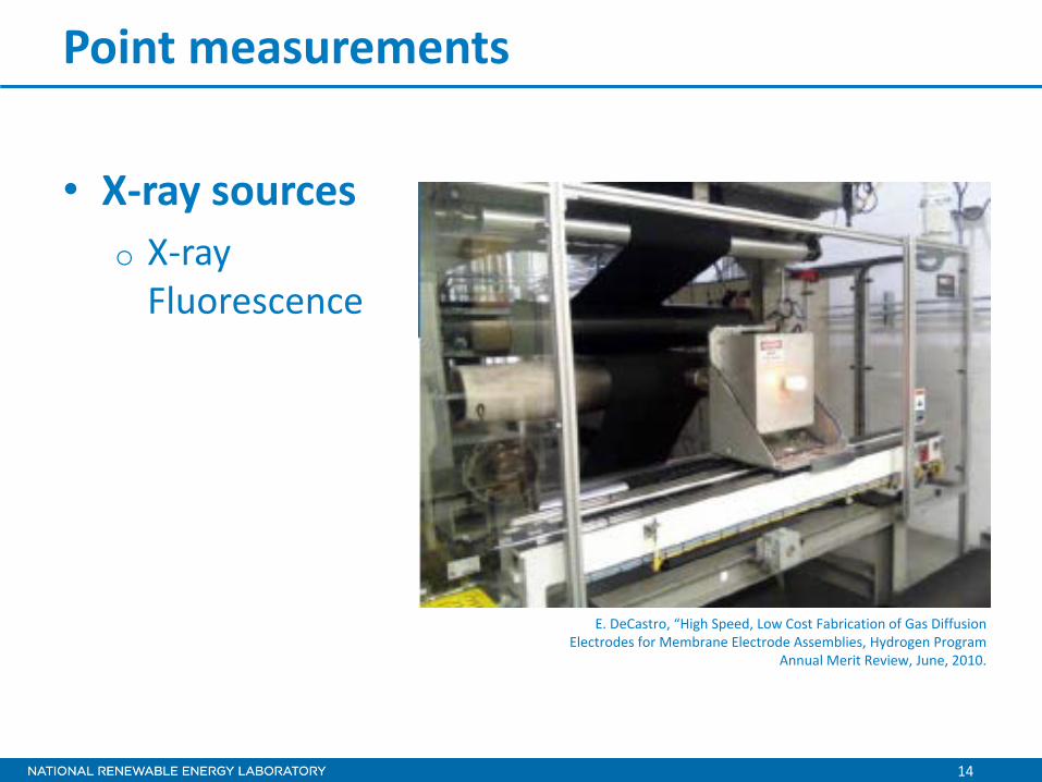
Point measurements
• X-ray sources o X-ray
Fluorescence
E. DeCastro, “High Speed, Low Cost Fabrication of Gas Diffusion Electrodes for Membrane Electrode Assemblies, Hydrogen Program
Annual Merit Review, June, 2010.
15
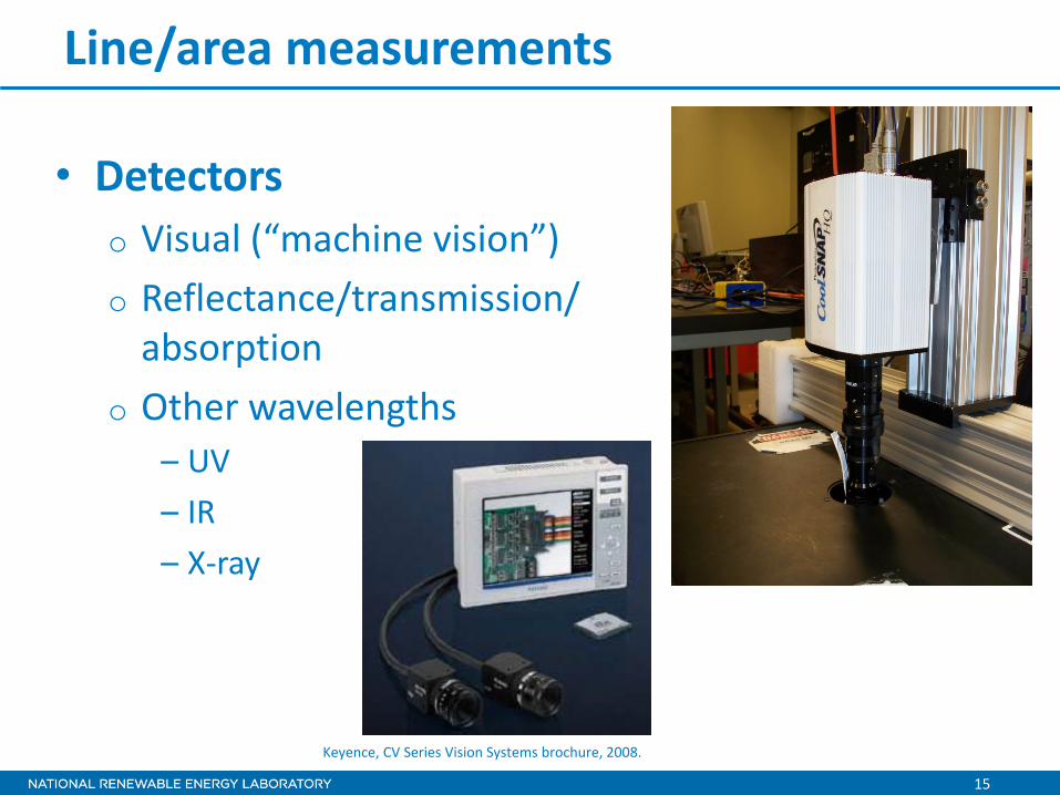
Line/area measurements
• Detectors o Visual (“machine vision”) o Reflectance/transmission/
absorption o Other wavelengths
– UV – IR – X-ray
Keyence, CV Series Vision Systems brochure, 2008.
16
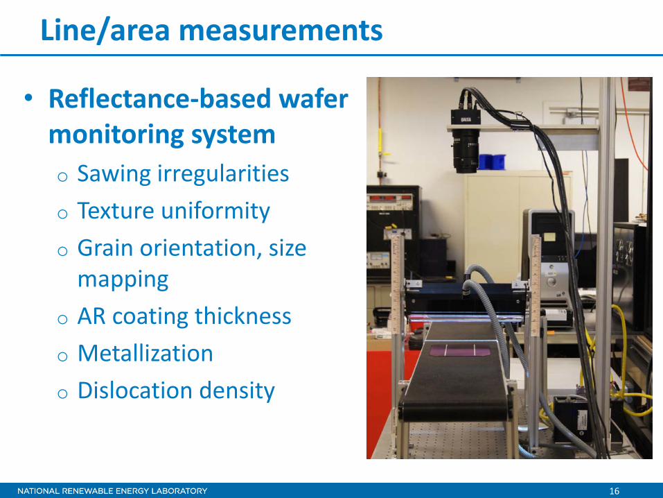
Line/area measurements
• Reflectance-based wafer monitoring system o Sawing irregularities o Texture uniformity o Grain orientation, size
mapping o AR coating thickness o Metallization o Dislocation density
17
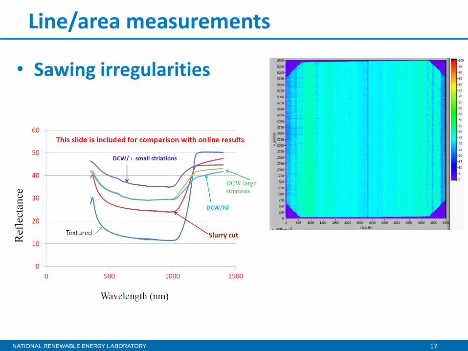
Line/area measurements
• Sawing irregularities
18
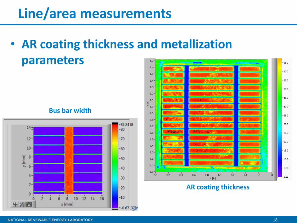
Line/area measurements
• AR coating thickness and metallization parameters
AR coating thickness
Bus bar width
19
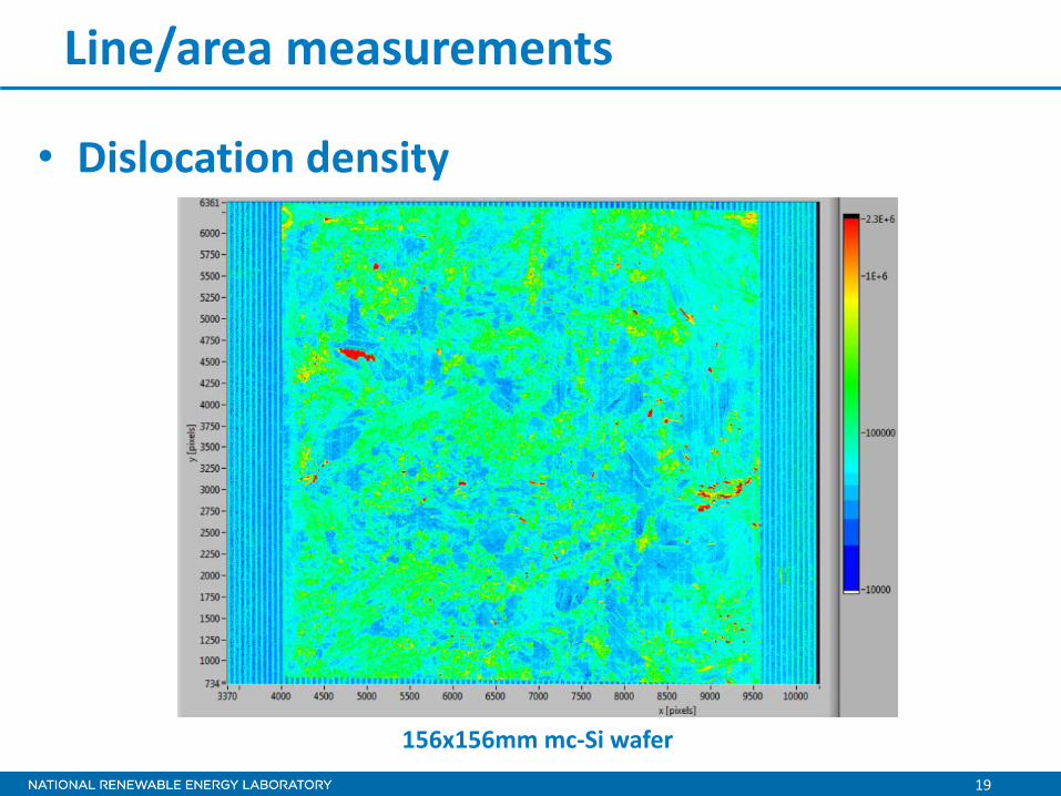
Line/area measurements
• Dislocation density
156x156mm mc-Si wafer
20
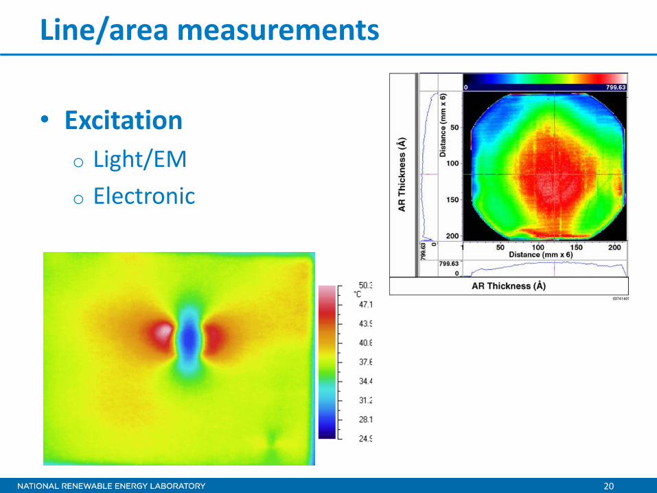
Line/area measurements
• Excitation o Light/EM o Electronic
21
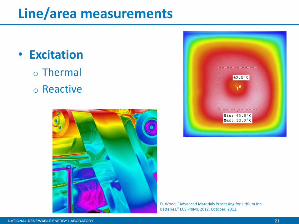
Line/area measurements
• Excitation o Thermal o Reactive
D. Wood, “Advanced Materials Processing for Lithium Ion Batteries,” ECS PRiME 2012, October, 2012.
![[6450-01-P] DEPARTMENT OF ENERGY 10 CFR Part 430 EERE … · DEPARTMENT OF ENERGY 10 CFR Part 430 EERE-2019-BT-STD-0022 RIN 1904-AE76 Energy Conservation Program: Energy Conservation](https://static.documents.pub/doc/80x56/5f2fda8dc3442b37045c042c/6450-01-p-department-of-energy-10-cfr-part-430-eere-department-of-energy-10-cfr.jpg)


