Effect of Conductor Surface Roughness upon Measured Loss and Extracted Values of PCB Laminate Material Dissipation Factor Scott Hinaga Technical Leader, PCB Technology Group Cisco Systems, Inc. San Jose, CA 95134 Marina Y. Koledintseva, Praveen K. R. Anmula, James L. Drewniak EMC Laboratory, Missouri University of Science & Technology Rolla, MO 65401 Abstract Prediction of accurate values for insertion loss (S 21 ) on printed circuit boards has become ever more critical to SI modeling as signal speeds required for next-generation networking equipment move into the 10+ GHz range. Existing industry-standard insertion loss estimation techniques assume that the copper conductors (PCB traces) are smooth, when in fact they are not. The error thus induced is less significant at lower speeds, but cannot be ignored at frequencies above a few GHz. Accurate estimation of PCB laminate dissipation factor (Df) is another goal integral to SI modeling. Industry-standard methods again assume the smooth copper case, with consequent frequency-dependent error introduced into extracted values of Df. This paper describes a set of stripline PCB test vehicles used to correlate copper trace surface roughness to insertion loss. The main errors induced in extracted values of Df resulting from increased conductor losses due to surface roughness have been analyzed. 1. Introduction 2. Copper Surface Texture in PCB Manufacture 3. Description of PCB Test Vehicle 4. Description of Test Equipment and Technique 5. Measurement Results – Total Loss 6. Relative Influence of Foil Type and Surface Treatment Type 7. Effect of Roughness on Modeled Conductor Loss (α c ) 8. Extraction of Df using Corrected α c and Induced Error in Df Values 9. Follow-on Work Introduction Increasing on-board signal speeds in the telecom industry, in some cases exceeding 10 GHz, are driving the need for leading-edge network infrastructure products to move away from conventional FR-4 laminates. The main reason for this is that the dissipation factor (Df) of such materials is rapidly becoming inadequate to maintain required levels of signal integrity. Total loss, as physically measured on a Vector Network Analyzer (VNA) or other instrument, comprises the sum of conductor loss (α c ) and dielectric loss (α d ). The property of interest, Df, is derived solely from the dielectric loss term. It is not possible in practical terms to make separate and independent measurements of α c or α d. . For this reason, the existing industry-standard Df extraction algorithms call for an empirical estimation of the value of α c , which is subtracted from the measured total loss, thus yielding the value of α d from which Df can then be derived. A known defect of the existing algorithms is that they assume that the copper conductor (trace) is perfectly smooth. At typical PCB trace dimensions (75-175 μm wide and 15-35μm thick), and at speeds below 1 GHz, the effect of surface roughness upon the error in Df is small. However as frequencies approach 10 GHz; the skin effect region becomes sufficiently shallow so as to drive a significant fraction of the current flow into the surface texture features, thus resulting in an actual value of α c which is considerably higher than that modeled in the smooth copper case. This paper describes insertion loss measurements performed on a 3x3 matrix of balanced single-stripline test vehicles differing only in the degree of roughness of the inner-layer copper foil. The factors that affect the surface roughness are the inherent roughness of the foil itself, and the surface-treatment-induced roughness intended to enhance inner-layer adhesion. The matrix allows for relative weighting of these two contributions to roughness for each test sample. All other relevant variables, such as
Transcript
Effect of Conductor Surface Roughness upon Measured Loss and Extracted Values
of PCB Laminate Material Dissipation Factor
Scott Hinaga
Technical Leader, PCB Technology Group
Cisco Systems, Inc.
San Jose, CA 95134
Marina Y. Koledintseva, Praveen K. R. Anmula, James L. Drewniak
EMC Laboratory, Missouri University of Science & Technology
Rolla, MO 65401
Abstract
Prediction of accurate values for insertion loss (S21) on printed circuit boards has become ever more critical to SI modeling as
signal speeds required for next-generation networking equipment move into the 10+ GHz range. Existing industry-standard
insertion loss estimation techniques assume that the copper conductors (PCB traces) are smooth, when in fact they are not. The
error thus induced is less significant at lower speeds, but cannot be ignored at frequencies above a few GHz. Accurate
estimation of PCB laminate dissipation factor (Df) is another goal integral to SI modeling. Industry-standard methods again
assume the smooth copper case, with consequent frequency-dependent error introduced into extracted values of Df. This paper
describes a set of stripline PCB test vehicles used to correlate copper trace surface roughness to insertion loss. The main errors
induced in extracted values of Df resulting from increased conductor losses due to surface roughness have been analyzed.
1. Introduction
2. Copper Surface Texture in PCB Manufacture
3. Description of PCB Test Vehicle
4. Description of Test Equipment and Technique
5. Measurement Results – Total Loss
6. Relative Influence of Foil Type and Surface Treatment Type
7. Effect of Roughness on Modeled Conductor Loss (αc)
8. Extraction of Df using Corrected αc and Induced Error in Df Values
9. Follow-on Work
Introduction
Increasing on-board signal speeds in the telecom industry, in some cases exceeding 10 GHz, are driving the need for
leading-edge network infrastructure products to move away from conventional FR-4 laminates. The main reason for this is that
the dissipation factor (Df) of such materials is rapidly becoming inadequate to maintain required levels of signal integrity.
Total loss, as physically measured on a Vector Network Analyzer (VNA) or other instrument, comprises the sum of conductor
loss (αc) and dielectric loss (αd). The property of interest, Df, is derived solely from the dielectric loss term. It is not possible in
practical terms to make separate and independent measurements of αc or αd.. For this reason, the existing industry-standard Df
extraction algorithms call for an empirical estimation of the value of αc, which is subtracted from the measured total loss, thus
yielding the value of αd from which Df can then be derived.
A known defect of the existing algorithms is that they assume that the copper conductor (trace) is perfectly smooth. At typical
PCB trace dimensions (75-175 µm wide and 15-35µm thick), and at speeds below 1 GHz, the effect of surface roughness upon
the error in Df is small. However as frequencies approach 10 GHz; the skin effect region becomes sufficiently shallow so as to
drive a significant fraction of the current flow into the surface texture features, thus resulting in an actual value of αc which is
considerably higher than that modeled in the smooth copper case.
This paper describes insertion loss measurements performed on a 3x3 matrix of balanced single-stripline test vehicles differing
only in the degree of roughness of the inner-layer copper foil. The factors that affect the surface roughness are the inherent
roughness of the foil itself, and the surface-treatment-induced roughness intended to enhance inner-layer adhesion. The matrix
allows for relative weighting of these two contributions to roughness for each test sample. All other relevant variables, such as
the PCB stackup (glass cloth style and resin content), trace dimensions and dielectric thickness, were kept constant. This was
done so that any measured differences in αc would originate only from the varying surface textures of the inner-layer traces.
The effect exerted by deviation from ideal αc upon extracted values of Df is also demonstrated in this paper. In the worst
(roughest surface) case, the assumption of a perfectly smooth copper trace results in a Df deviation of nearly 50% from the
result calculated using our preferred algorithm.
Copper Surface Texture in PCB Manufacture Smooth copper is never used in actual practice, though it would be theoretically possible to manufacture a multilayer PCB using
inner-layer copper with a very close to perfectly smooth finish. In the case of a mirror-bright surface, foil-to-resin adhesion
would be compromised, thus increasing the propensity of the board to delaminate during the thermal stresses of the PCB
assembly process.
Typically, the “teeth” on the surface of foils that face the interior of the laminate (core material) “sandwich” can be up to 8µm
in depth, while the exterior of the foil may be fairly smooth. Such foils are referred to as Electrodeposited (ED) or Standard foil.
However, in a well-known industry variant, namely, Reverse-Treated Foil (RTF), both sides of the copper foil may have
smaller-sized “teeth” on both the interior- and exterior-facing sides with regard to the laminated core material.
In addition to the two above-mentioned types, some newer foils on the market aimed specifically at loss reduction are offered
on certain low-loss laminate systems. These are variants of ED foil with smaller average tooth sizes, and their proprietary
designations are VLP (Very Low Profile), as well as SVLP/HVLP (Super / Hyper Very Low Profile).
Figure 1
Typical inner-layer trace showing degree of Cu
roughness on upper and lower surfaces
In any case, the PCB fabricator, after etching the circuit patterns onto both sides of the inner-layer core, will then apply an
adhesion-promoting surface treatment to the copper circuitry prior to laminating the cores together to form the complete
multilayer package. The traditional surface treatment, referred to as “Reduced Oxide”, consists of a hot, highly alkaline,
oxidizer bath which forms a thin layer of cupric oxide on top of the copper surfaces. The panel is then rinsed and immersed into
a reducer bath which partially reverses the process, thinning the oxide layer and reducing much of it back to copper metal.
Compared to bare copper, the oxide provides a more optimal surface for adhesion of the molten prepreg resin during the
subsequent lamination step. In practice, such Reduced Oxide processes can either be purchased as a proprietary package from
chemical suppliers, or carried out using well-known generic formulations.
Automation and conveyorization are important to maximize manufacturing throughput. However, the Reduced Oxide process
is not easily amenable to automation and conveyorization. To overcome this problem, PCB chemical suppliers have developed
a new family of chemistries referred to as “Oxide Alternatives”, which have found wide popularity throughout the industry.
These systems consist of a sulfuric acid solution, combined with hydrogen peroxide as the oxidizing agent, with proprietary
stabilizers and rate inhibitors added by the chemical suppliers to control the rate of reaction. The acidified peroxide selectively
corrodes the copper surface, etching downward along the grain boundaries of the crystalline structure of the copper foil.
Because the corrosion occurs more quickly along such grain boundaries, the result is a surface comprised of peaks and valleys.
This surface topography enhances adhesion of prepreg resin as in the case above. The various processes may also co-deposit an
organic coating on the exterior surface to further enhance chemical bonding by the resin.
The differing chemical mechanisms of the two types of processes have an impact on the loss phenomena associated with
surface roughness. The Oxide process builds up essentially nonconductive cupric oxide crystals upward from the base copper
surface, such that there is no current flow within the oxide layer itself. In contrast, by etching “valleys” downward into the base
copper, the Oxide Alternative processes create a texturized surface which does intrude down into the region of skin effect.
Therefore, as will be demonstrated in the paper, a traditional Oxide process has a smaller impact on roughness-induced loss as
compared to the Oxide Alternative processes.
Description of PCB Test Vehicle
A PCB test vehicle used by Cisco for electrical property investigation is shown in Figure 2. The test trace length is 406mm
(16”) with launch structures on both ends. This is a 6-layer balanced-stripline configuration with solid reference planes on
layers 1, 3, 4 and 6, single striplines on layer 2, and differential pairs on layer 5. Total board thickness is built up to a nominal
2.4mm (0.093”).
Figure 2
Overview of the test vehicle showing fixturing locations for SMA connectors
Except for the dielectric between layers 3 and 4, which is nonfunctional, the other four openings (two core and two prepreg) are
matched as to glass style and resin content. The target resin content is 50%, which, depending on the material under test,
typically results in the use of 2-ply of 2116 or 3313 glass.
There are three single striplines on layer 2 whose widths are tuned for target impedances of 48, 50 and 52 ohms. Likewise, three
differential pairs are present on layer 5, tuned for 96, 100 and 104 ohms. However, impedance control at any PCB maker is
subject to process variation due to irregularities in line width and pressed dielectric thickness. The additional traces bracketing
the ideal values of 50 and 100 ohms provide opportunities for salvaging individual boards whose impedance is off either high or
low from the target value. To minimize reflective (S11) losses, we imposed an unusually tight impedance tolerance of ±5% as
compared to the industry-standard ±10%.
The launch structure is a surface pad designed to accept a flange-mount, compression-fit SMA connector. Centered in the pad
is a via drilled with an 0.25mm (0.0098”) tool. The outer-layer pad, present on both layers 1 and 6, is 0.030” (0.765mm) in
diameter, and the inner-layer pad connecting to the signal trace on layer 2 or 5 is 0.019” (0.484mm) in diameter. Clearances of
0.100” (2.54mm) diameter isolate the signal via from the four plane layers.
Figure 3
SMA connector, Molex 73251-1850
The return path is provided by the metal SMA connector body, which contacts the external plane layer via two mounting bolts
providing a compression fit. The two mounting plated-through holes are drilled directly through the four plane layers. A circle
of eight ground stitching vias that pass through the four ground planes is located just outside the clearance diameter. This circle
provides shielding for the launch structure and further enhances the return path.
The SMA connector is mounted on the far side of the PCB in order to minimize via stub length (e.g., when testing the traces on
layer 2, the connector is mounted against layer 6). Thus, the length of the via stub is limited to approximately 0.25mm (0.010”)
with the actual length varying somewhat depending on the laminate material under test. Parasitics due to this stub limit the
maximum useful frequency of the test vehicle to ~18 GHz. While it would be possible to increase this maximum frequency by
back-drilling the stub, board-to-board variation in stub length would introduce an additional source of undesirable variability.
For this reason, the stubs were not removed in this project.
In addition to the test traces, a number of calibration traces are also present on layer 2 to permit the use of the TRL
(Through-Reflect-Line) calibration technique, described further in the next section. All these calibration traces are tuned for
50-ohm characteristic impedance. These are of fixed lengths of 5” (127mm), 10” (254mm), with four additional traces whose
lengths vary depending on the expected dielectric constant (Dk) of the particular laminate material under test. The method also
requires a trace of 0.59” (150mm) to serve as a “Through” standard, and an unterminated stub of 0.295” (75mm) to serve as an
“Open” standard.
Non-generic features of the test vehicle specific to this project are as follows:
The laminate chosen was “Megtron-6” (R-5775K) manufactured by Panasonic (Matsushita Electric Works, Osaka, JP) . This is
one of a small group of high-performance products introduced fairly recently. Such materials feature very low Df at a level
approaching that of older systems based on PTFE or polybutadiene. However, they are more amenable to thick,
high-layer-count boards as compared to these earlier product types, particularly with regards to thermal durability.
Megtron-6 core material is offered with three types of copper foil: Standard ED foil, VLP and HVLP, whose surface profile has
an average roughness of approximately 8, 3 and 1.5µm, respectively. These foils are available in several different copper
weights, but since the only weight common across all three foil types is H-oz (18 µm), this weight was selected for use.
In order to minimize variation between samples, it was highly desirable to manufacture the set of test vehicles utilizing single
lots of prepreg and core material, and as a single lot through the PCB fabrication process. This latter necessitated the use of a
PCB fabrication shop which had multiple inner-layer process lines. The shop selected from our PCB fabrication supply base
was equipped with three such processes:
1. Conventional Reduced Oxide of a generic formulation.
2. Multibond 100ZK, a proprietary Oxide Alternative supplied by MacDermid Inc. (Denver, CO) which is based on
sulfuric acid / hydrogen peroxide.
3. Etchbond CZ8100, another sulfuric / peroxide-based Oxide Alternative supplied by MEC Co., Ltd. (Amagasaki, JP).
The combination of the three types of foil and the three types of inner-layer surface treatment thus required the manufacture of
nine sample sets.
Description of Test Equipment and Technique The instrument used for loss measurement is a two-port Agilent PNA vector network analyzer, model E8364B, equipped with
2.4 mm cables, 72” (1.83m) in length, rated to 50 GHz (W.L. Gore, P/N 0Z0CJ0CJ072.0)
Figure 4
Overview of VNA and cable setup
The flange-mount SMA connectors used are Molex P/N 73251-1850. Prior to each measurement, the VNA was allowed to
warm up and stabilize for a minimum of 2.5 hours.
Calibration of a VNA is required in order to de-embed the loss, phase lag and other effects induced by the cabling and
connectors. For PCB work, such calibration is often carried out using the SOLT (Short, Open, Line, Thru) technique, in which
external calibration standard loads (“standards”) are connected to the VNA cables. Systematic error corrections are then
applied by the VNA software to de-embed the effects associated with these calibration standards having known parameters.
However, this technique is somewhat less accurate than our preferred TRL (Through-Reflect-Line) method. This is because the
calibration standard for the latter consists of purpose-designed calibration traces built into the test vehicle itself. Thus the TRL
calibration allows for de-embedding any systematic errors inherent to the test vehicle structure, such as those associated with
the capacitance and inductance of the launch vias, and any anisotropic effects due to the fact that PCB laminate material is
inhomogeneous. As noted previously, the test vehicle was designed with a total of eight TRL calibration traces built-in, so as to
allow the use of this more accurate technique. The frequency breakpoints for the TRL calibration fell at 50.00 MHz, 281.17
MHz, 1.581 GHz, and 8.891 GHz.
During calibration and measurement, the cables were attached to the SMA connectors using a torque wrench in order to
minimize variation in contact resistance. The temperature in the test area was maintained within a range of 18 to 23 °C, and a
relative humidity of 35 to 40 %.
The nine types of boards with different foil + oxide/oxide alternative combinations were then tested, with three samples of each
type of board (27 boards in total). Prior to the actual S21 loss measurements, two validation checks were performed on all 27
sample boards to ensure compliance with Cisco’s specifications. The first validation check was an impedance verification. The
impedance of the 16” single-ended striplines was measured using an Agilent DCA 86100C digital communications analyzer.
For all 27 boards, it was verified that the line impedance fell within the 50 ±5% limits. Then the best impedance-matched line
was selected for each of the nine types of boards.
These nine selected lines were further validated by taking d.c. resistance measurements using an LCR meter, HP4263B. A
range of 1569 to 1835 mΩ was observed. While this range was somewhat larger than desired, it does serve as a useful reminder
of the degree of board-to-board variation that one encounters in actual practice.
One board of each of the nine types was chosen as a “sacrificial” board, which was cut to examine a cross-section using
micrograph pictures. These cross-sections were taken at identical locations. The trace widths, thicknesses, and dielectric
spacing were validated as falling within the planned tolerances. The microsections allowed for dimensional measurement
comparison of the traces and the surface roughness feature sizes, as in Fig. 1. It was thus confirmed that the average roughness
was in line with that claimed by the foil manufacturers and chemical process suppliers. These values are presented in Table 1.
Table 1
Amplitude of roughness (Ra) with respect to different foil and oxide types
Foil type Roughness Oxide type Roughness
Standard foil 7-8 µm Reduced Oxide <1 µm
VLP foil 3-4 µm Multibond 100ZK 1-2 µm
HVLP foil 1.5-2 µm Etchbond CZ8100 1.5-3 µm
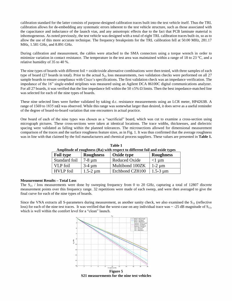
Measurement Results – Total Loss
The S21 / loss measurements were done by sweeping frequency from 0 to 20 GHz, capturing a total of 12807 discrete
measurement points over this frequency range. 32 repetitions were made of each sweep, and were then averaged to give the
final curve for each of the nine types of boards.
Since the VNA extracts all S-parameters during measurement, as another sanity check, we also examined the S11 (reflective
loss) for each of the nine test traces. It was verified that the worst-case on any individual trace was ~ -25 dB magnitude of S11,
which is well within the comfort level for a “clean” launch.
Figure 5
S21 measurements for the nine test vehicles
Relative Influence of Foil Type and Surface Treatment Type
The order of the measured loss results obtained when studying the relative influence of foil type and surface treatment fell
within expectations. As Standard foil has the largest average roughness, the three samples with this foil had far greater loss than
any of the other six. Within this group of three types of Standard foil, the order ranked by surface treatment type was
loss with Black Oxide < loss with MB100ZK < loss with CZ8100.
Samples with VLP exhibited higher loss than those with HVLP, but the performance difference eroded (literally) with the
application of a high-roughness surface treatment. With oxide applied, HVLP outperformed VLP by ~ 7-8%, while with
CZ8100 applied, that gap fell to only ~2%.
The results of relative loss at three target frequencies of specific interest are presented in Table 2.
Table 2 -- Sample losses normalized to Nepers / meter
It is evident from the data in the Table that there is not much difference in performance between Oxide and MB100ZK on the
two low-profile foils, while there is a slightly larger (2-6 %) advantage for Oxide on Standard foil. These differences may be
due to MB100ZK not acting upon the various foils in an identical manner. The larger grain structure of the Standard foil may
enhance the etching action of this particular peroxide / sulfuric acid chemistry, thus leading to a more pronounced surface
texture and thus higher loss. Unfortunately, the difference in loss is so small that it does not correspond to a visible difference
that can be observed on SEM micrographs of the respective surfaces.
More significant is the difference between the best (HVLP + Oxide) and the worst (Standard + CZ8100) cases. At 10GHz, the
corresponding loss of 1.807 and 2.707 Np/m represent a 50% differential. If two different fab suppliers manufacturing the same
PCB part number were to use these two combinations, there could result a post-assembly situation wherein boards from
supplier “A” would pass SI-related functional testing, while those from supplier “B” would fail. At higher speeds, even smaller
differences might be magnified to such a degree as to result in an SI-related performance failure.
Effect of Roughness on Modeled Conductor Loss (αc)
The authors have been refining an algorithm for the extraction of Df from S21 data. All such algorithms proceed from a
foundation of total loss (αt), the actual loss figure measured using a VNA, which is equal to the sum of conductor loss (αc) and
dielectric loss (αd). As there is no direct measurement technique to physically separate these two components, the existing
algorithms for Df account for the value of αc based on simulations derived from the geometry of the line. This αc value is then
subtracted from the measured αt, yielding the figure for αd, from which the value of Df may be extracted.
Any inaccuracy in αc will result in a corresponding inverse inaccuracy in αd, and it is here that the neglect of surface roughness
in αc comes into play. A survey of various suppliers to the PCB industry reveals that, with the exception of certain specialty
laminators targeting the microwave industry who are aware of the roughness issue, the principal test methods used are IPC
2.5.5.5 (Stripline Test for Permittivity and Loss Tangent at X-Band)1 and an updated variant, IPC 2.5.5.5.1. In these resonant
cavity measurement methods, the resonant frequency (fr) is first found. Frequencies f1 and f2 offset to the left and right of the
resonant frequency are defined as corresponding to an SWR power meter reading at a level of -3 dB from the resonant frequency peak. These readings are then denoted as dB1 and dB2. Df, also referred to as loss tangent (tan δ), is then expressed as
Frequency 3GHz 5GHz 10GHz
HVLP + Oxide 0.652 0.985 1.807
HVLP + MB100ZK 0.656 0.986 1.827
HVLP + CZ8100 0.690 1.042 1.926
VLP + Oxide 0.698 1.054 1.951
VLP + MB100ZK 0.696 1.054 1.943
VLP + CZ8100 0.698 1.061 1.959
Standard + Oxide 0.822 1.297 2.475
Standard + MB100ZK 0.837 1.331 2.579
Standard + CZ8100 0.881 1.406 2.707
,1
110
1
110
1
tan
10
2
10
1
21c
dB
r
dB
r
Q
f
f
f
f
The method then defines the term 1/Qc as:
,1
rr
c
c f
c
Q
where c is the speed of light in free space, εr is the relative dielectric constant of the substrate, and f r is the resonant frequency.
The attenuation constant due to the conductor loss αc, is then defined as
,377
42 B
YZR ors
c
where Rs is the surface resistivity of Cu (ohms), Zo is the wave impedance of the resonator, B is the dielectric gap to the ground
plane, and Y, defined below, is a factor based on the width (W) and thickness (T) of the stripline.
,1
1
log12 2
2
X
X
B
TX
B
WXXY e where .
TB
BX
The wave impedance Zo is then defined as:
,
4
377
TB
WC
Z
fr
o
introducing a new term, Cf, which, similarly to Y, is based on physical geometry of the stripline:
,
1log11log2 2
XXXXC ee
f where again, .TB
BX
As can be seen in examining the component variables of αc, the expression does not include a term for copper surface roughness.
The calculation of αc is based solely upon stripline geometry, dielectric constant and surface resistivity; assuming an ideally
smooth conductor, it does not include any accounting for the surface texture of the copper trace. The text of the test method
admits as much, stating in paragraph 7.2.1: “Data is not currently available for correcting this calculated value [1/Qc] to
account for the increased conductor loss due to surface treatments or type of copper used.” Furthermore, it is impossible to
separate the discrete contributions from conductor loss and dielectric loss.
A second loss measurement and Df extraction technique well-known in the industry is the Bereskin Stripline test method2, in
which a signal source is used to excite oscillations in an isolated stripline. The oscillations are then coupled into a detector
whose output is monitored by a power meter. Like the previous methods, the Bereskin technique requires finding the
fundamental resonant frequency of the test sample, with the frequency then varied off to either side of resonance in order to
find those frequencies, Flow and Fhigh, corresponding to a -3dB power level from that at resonance. These two terms are therefore
seen to be equivalent to the f1 and f2 of the previous method. There are other similarities to IPC 2.5.5.5 and 2.5.5.5.1 in the
calculation of Df (tan δ). The IPC methods state that a less exact approximation of tan δ may be given as
cr Qf
ff 1tan 21
or
cQQ
11tan
Bereskin modified this by introducing the square root of the resonant frequency to the denominator of the last term,
omo fQQD
11
While the naming of variables is different (D for tan δ, Qmo for Qc, and ƒo for fr), it is apparent that the Bereskin expression for
Df contains the same underlying variables as seen in IPC 2.5.5.5 and 2.5.5.5.1.
The IPC and Bereskin stripline methods belong to the class of cavity-resonator-type techniques, which are comparatively
narrowband, requiring construction of a set of tuned test samples to span a wider frequency range. There is a discrete spectrum
of resonances (resonance lines) in the cavity over a given frequency range of operation, so measurements take place at
individual frequency points and must then be interpolated. Q-factor decrease and frequency shift for each resonance line in a
stripline loaded with a sample compared to the empty structure give information about Df and Dk, respectively. The
fundamental shortcoming of resonator-type methods is that the data is available only at these discrete frequencies - it cannot be
a continuous function. The other problem is the decrease of accuracy of measurements with an increase of resonance peak order,
especially for samples with increased loss, e.g. > 5 Np/m, or a Df > 0.01.
The fundamental mode in an empty cavity produces a resonance peak at the lowest frequency, below which there is a cut-off.
This is the most intense and sharpest peak with the highest Q-factor. All succeeding peaks are of lower intensity: as frequency
increases, Q-factors of these peaks decrease. This is due to increased loss in a realistic structure with metal walls (especially if
they are not ideally smooth) as frequency increases, causing faster damping of higher-frequency oscillations, and less effective
excitation (matching) of higher-order modes by the source.
When the structure is loaded by a sample, it is more difficult to accurately measure peak resonance frequency shifts and
reduction in Q-factors at higher frequencies than at lower. This is because initial tops of higher-order peaks are flatter (more
broadened) than for the fundamental and lower-order peaks, thus making it more difficult to accurately locate the true
maximum of the peak and its corresponding frequency. This might lead to underestimation of measured values. A similar
problem is seen with measuring widths of the resonance lines at the -3 dB level. Unloaded widths are larger at higher
frequencies. Loaded resonance lines at higher frequencies become even wider, substantially wider than desirable accuracy
would allow.
By contrast, the currently-described method uses only a single test sample to cover a comparatively wide frequency range.
More than twelve thousand discrete points are generated through VNA measurements at equal intervals along the
entire frequency spectrum, thus yielding a curve which for practical purposes, may be treated as continuous.
The MST/Cisco test method is based on transmission line theory and does take into account roughness-induced loss. Therefore,
any associated expression for calculation of αc which includes a term based on average surface roughness can be cross-checked
against the actual measured results from the nine test specimens. An assumption for the present study is that the value of αd
should be constant across all 9 samples. The reasoning for this is that they were fabricated simultaneously from the same lots of
core and prepreg material, such that the finished resin content should vary to a negligible degree. Thus the samples would differ
solely with respect to conductor loss. Substituting the measured physical dimensions and the impedance from the test vehicles
into the expression for αc gives a theoretical curve, which can be overlaid upon the empirically-generated one.
Our preferred mathematical expression for αc which includes terms for surface roughness, originated with Sami Sundstroem:3
where
βo is the propagation constant in free space;
ηo is the characteristic impedance of free space (376.73 Ω);
p is the perimeter of the stripline’s cross-section, equal to 2 (thickness + width of the trace);
Zo is the wave impedance of the stripline under test (measured average value used);
1
2224442 42
11
1
4 n
n
o
ooc snsnH
pZ
δ= sqrt(ρ/πfμ), the skin effect depth at a given frequency, where ρ = resistivity of the copper trace in Ωm-1
, f = frequency in Hz,
and μ = μo · μr, the absolute permeability of copper, which is almost the same as that for vacuum (μo=1.25710-6
H/m), since
copper is a diamagnetic metal;
Hn = A(-1)n-1
/nπ, the magnitude of the nth
harmonic of the surface function, where A is the mean peak-to-valley magnitude of
the surface roughness function;
s= 2π / Λ is the geometrical analog of wave number, where Λ is the mean periodicity of roughness, which is assumed to be the
same along all three dimensions. This is basically the average distance between two neighboring peaks.
Using the above expression, it is possible to make a direct correlation of total measured loss to αc. This expression has two
terms: the first describes an absolutely smooth conductor, and the second is related to the surface roughness function expanded
in a Fourier series through harmonics of amplitudes Hn, provided that the surface roughness is approximated by a periodic
function. In our computations, the number of harmonics is n 1,000 for a saw-tooth function, approximating a realistic surface
roughness.
We consider the Sundstroem equation to be a refinement of the earlier work of Hammerstad4, which accounts for surface
roughness in a semi-empirical fashion. This equation applies a roughness-based coefficient to the smooth-case value of αc
,4.1arctan2
1
2
0
cc
where Δ is the RMS surface roughness (equal to A/2), and δ is the skin depth. However, this equation does not deal with
realistic roughness as a function of X-Y coordinates -- it does not allow for separating amplitude and periodicity (A and Λ).
Brauninsch et al5 describe a way of taking into account surface roughness through small perturbations and calculating spatial
power spectral density (PSD) corresponding to the statistical values of roughness. However, the procedure required to extract
this PSD is complex, so we prefer the simpler Sundstroem equation, even though the latter necessitates using an approximate
deterministic periodic function to describe surface roughness.
Literature from copper foil manufacturers and from Oxide Alternative chemical suppliers expresses roughness values in one of
two terms, Rz (maximum roughness), or Ra (average roughness). While Ra is the more useful of the two for our analysis, it does
not present the full story, as measurements of Ra are typically conducted by optical or contact profilometry and principally
represent a measurement of A. To obtain accurate values of Λ, it is preferred to take measurements from a cross-sectioned
conductor at high magnification, or from a SEM micrograph of the surface in question.
Sundstroem’s equation assumes that the surface of the trace / conductor is uniform in roughness, but of course, this is not the
case in the PCB world. Several approximations must be made to account for the fact that the upper and lower surfaces of the
trace have different values of A and Λ. First is the fact that a PCB inner-layer trace is trapezoidal rather than rectangular in
cross-section, a natural and expected result of the inner-layer etching process. The lower face (base, or foot) representing the
foil texture is thus wider than the upper face (top) which bears the texture of the oxide or oxide alternative. The difference in
width is influenced by the PCB etching process, but it also depends upon copper foil weight (thickness): the thicker the copper,
the more pronounced the top-bottom difference. In our test vehicle set based on H-oz (18 µm) copper foil, the cross-sectional
trace measurements showed a 13.44-mil (0.336-mm) mean width at the base of the trace, with the tops of the traces reduced in
width by 0.08-0.24 mils (0.002-0.006mm). Thus the effective difference between the bottom and the top of the trace is on the
order of 1%. In practice, this is a best case, since the traces on our test vehicle are considerably wider than those seen on typical
boards, which may be as narrow as 3.5 mils nominal (0.0875mm). Since such fine traces will always call for H-oz (18 µm) foil,
the same as our test vehicle, we can estimate that the mean 0.16 mil (0.004mm) reduction in top width would represent a
top-bottom difference of 5% on a 3.5-mil trace. In such cases, the effective values of A and Λ would need to be proportionally
weighted to the top and bottom widths, as shown in Fig. 6,
and likewise with Λ
,
bottomtop
bottombottom
bottomtop
top
topeffWW
WA
WW
WAA
,
bottomtop
bottombottom
bottomtop
top
topeffWW
W
WW
W
Figure 6.
Trace dimensions and surface roughness of the trace
The surface current on the trace is distributed mainly on the top and bottom surfaces of the trace, with a negligibly small
proportion across its thickness, so the deviation of edge surfaces (sidewalls) from ideal smoothness may be safely neglected.
Sundstroem’s equation also assumes a balanced stripline configuration, in which the upper and lower surfaces of the trace are
equidistant from the two reference planes. The design of the test vehicle is intended to conform to this structure. The
cross-sectional measurements of dielectric thickness for the nine sample sets showed the L1-L2 dielectric (2 ply of 2116
prepreg) to be 11.79±0.28 mils (0.295±0.007mm), while L2-L3 (nominal 12-mil core material) measured at 12.64±0.15 mils
(0.316±0.004mm), a mean difference of just over 10%.
Since the surface current in a flat conductor parallel to a reference plane decreases with distance from the plane as the inverse
square, it is evident that an imbalance of 10% in side-to-side dielectric spacing will be more significant on stripline stackups
where the trace-to-plane dielectric spacing is smaller, say, on the order of 4 mils (0.1mm). In such cases, the structure would
preferably be treated as an unbalanced stripline, as per the case described below.
However, the difference in dielectric gap from the trace to the upper and the lower ground planes does not affect current
distribution on the top and bottom surfaces of the signal trace. It would matter only if taking into account surface roughness on
the ground planes themselves. However, in this analysis the surface roughness on the ground planes may be safely ignored,
since the current densities on the reference planes of the stripline are negligibly small compared to the current on the trace6. For
this reason, only roughness of the trace itself need be taken into account. If the trace is extremely close to one of the ground
planes (dielectric gap < 0.3 trace width or < 2 trace thickness, and < 0.5 the size of the larger gap on the other side), the
current on this plane would be substantially higher than on the other, and surface roughness on the ground plane would then
become sufficiently significant to take into account. However, in this particular study, the effect of roughness-induced loss due
to the ground planes need not be considered, since the above conditions are not met.
Extraction of Df using Modeled αc and Induced Error in Df Values
Based on examination of cross-sectional micrographs of the traces, it is possible to estimate the amplitude (A) and periodicity
(Λ) of the surface features for the three foils and three surface treatments. It can be seen from micrographs that for both top and
bottom surfaces the amplitude and periodicity are almost equal, A ≈ Λ. Using the previously-noted roughness values for the six
surfaces, the values of αc as a function of frequency were calculated and compared to the curve of αc obtained using our
preferred genetic algorithm optimization7. This optimization procedure was used for finding the coefficients and to separate
contributions of conductor and dielectric loss within the total loss:
where the conductor loss is known to behave as a square root of frequency due to skin-effect,
and the dielectric loss is directly proportional to the frequency
The total loss is obtained by S21 measurement using a VNA and calculation of the A parameter of the ABCD matrix, which is
related to the four measured S-parameters 8, expressed as
,t c d
,c
.d
From the complex propagation constant γ, which consists of real (α -- attenuation) and imaginary (jβ -- phase) parts, we
consider only the real part, α, in calculation of the total attenuation constant αc.8
1cosh ( )Re( ) Ret
A
l
.
where l is the electrical length of the conductor under test.
Figures 7 and 8 present the results for the worst (roughest) case – Standard foil + CZ8100, and the best (smoothest) case –
HVLP foil + Oxide. Fig. 9 shows that the curves calculated based on the Sundstroem equation and the genetic algorithm curve
fitting converge, when A and Λ approach zero.
While the curve generated by Sundstroem’s equation nearly overlays the simulated curve for the case of A and Λ approaching
zero, some deviation begins to appear when the physical measurements of the non-ideal test vehicles are introduced.
Comparing Fig. 7 and 8, one may observe that this deviation between the two methods increases in magnitude as roughness
increases. Sundstroem’s equation turns out to be more accurate for taking into account surface roughness than the genetic
algorithm curve fitting. In this analysis it was assumed that the surface roughness behaves as a saw-tooth function of
coordinates. However, in reality this may be not quite true, and the next stage of modeling will require considering the surface
roughness as a random function.
Figure 7
Modeled vs. measured αc for worst (roughest) case, Std + CZ8100
Figure 8
Modeled vs. measured for best (smoothest) case, HVLP + Oxide
11 22 12 21
21
1 1( )
2par
S S S SA S
S
Figure 9
Modeled vs. ideal-simulated for near-ideal case, Λ and A 0
Extraction of Df using Corrected αc and Induced Error in Df Values
Independent of the functionality of the theoretical model previously discussed, with measured values of roughness-dependent
αc in hand, it is possible to study the effect of the latter upon the calculated Df. As noted earlier, if roughness effects are ignored,
the simulated value of αc will be lower than the actual figure. This will result in an overestimated value of αd, and in turn will
cause the extracted value of Df to be higher than it should be. Conversely, it follows that by using a roughness-insensitive Df
extraction method, and constructing a test vehicle with copper foil smoother than Standard foil, an interested party could obtain
Df results for the laminate under test which would appear unrealistically low, unless clearly noted that Standard foil was not
used. In other words, a reduction in total measured loss (αt), due in fact to the smoother foil, could be improperly attributed to
the αd of the dielectric material, thus falsely reducing the extracted value of Df. The effect would be most apparent when trying
to compare the Df of several different materials which had not been built on comparable foil types.
To demonstrate this effect when extracting the Df value for Megtron-6 material, copper roughness was first ignored. Fig. 10
shows the extracted Df over the 0 - 20 GHz range for the best and worst of the nine samples using the Sundstroem model and the
extracted curve obtained by using αc, when surface roughness is ignored. Measured t values of course differ for these boards,
and since it was assumed that Dk was identical for all samples due to essentially constant resin content, any difference in the
extracted Df values for the samples should be due to surface roughness variation only. If surface roughness is ignored, the
results for Df are not correct. At the same time, application of the Sundstroem model implies that the values of A and Λ, as well
as the form of the surface roughness as a function of X-, Y- and Z-axis coordinates are known exactly. But estimations based on
micrographs alone do not give this exact information. For this reason, there is observed some difference in the extracted values
of the Df for these nine samples with identical dielectric. A more exact method for these estimations may be some type of 3-D
topographical mapping, optical interferometry, scanning probe microscopy and scanning electron microscopy (SEM).
When conductor surface roughness is considered, the deviation between the maximum and minimum values of the extracted
dissipation factor is less than 5% for the same material across the nine combinations of foil and oxide. However, if conductor
roughness is neglected, the deviation would be about 35%.
Figure 10
(a). Extracted values of “apparent” Df; (b). Magnified view around 10 GHz
Follow-on Work In the course of this project, a number of potential avenues for further investigation arose. While outside the scope of this
current paper, they would nonetheless be worthy of future study, should the opportunity arise.
Other Materials: The Panasonic Megtron-6 material was selected due to its being readily available during the timeframe for
test vehicle construction. However, a number of other laminate manufacturers around the world also offer competitive
materials, which match or approach this performance class. These materials are also either offered, or are planned to be offered,
with low-roughness copper foil. Replication of this testing with such materials would provide additional data points to refine
the Sundstroem model for αc, as well as allow for an assessment of the claimed Df values for these other laminates. We are
currently studying a number of such laminates.
Real-World Copper Effects: Skin depth is proportional as the inverse square root to the conductivity (σ) of the metallic copper
from which the conductor is fabricated. However, the copper foil used in PCBs is not elementally pure. Elements such as
phosphorous (P), antimony (Sb), arsenic (As), iron (Fe), tin (Sn), zinc (Zn), etc. may be deliberately or inadvertently
co-deposited by the manufacturer during the electroplating process9. These impurities disrupt the ideal crystal structure, leading
to the formation of grain boundaries of various shapes and sizes, and reduce conductivity compared to the nominal value of
5.818107 S/m. In attempting an “apples-to-apples” Df comparison of laminates made with different foil types, it would be
highly desirable to know the actual value of copper conductivity, as the effects on measured loss could then be de-embedded.
Dk Effects: While the focus of this project has been on dissipation factor, Df, the dielectric constant, Dk, of laminate materials
is of equal interest to the circuit designer. Dk is extracted from the phase component of the same S-parameter set obtained from
a VNA measurement. It is clear that for any dielectric, the phase and loss constants - β and αd - the imaginary and real parts of
the complex propagation constant γ, respectively - are not arbitrary, but interrelated. Therefore, the value of αd (and hence Df)
would affect β and Dk. Determining the copper surface roughness effect upon extracted values of Dk is planned as a topic for
further study.
Smooth Cu Model: With a conventionally-constructed PCB, the smoothest available copper model is the HVLP + Oxide
combination. However, we considered whether it would be theoretically possible to construct a test vehicle even closer to ideal
by using the specialized Multiwire technique, in which copper wires of round cross-section are laminated into the PCB to form
the conductors, taking the place of etched circuit patterns. Some modification of the process would be necessary – the wire
employed is coated with an insulating varnish whose Dk and Df would need to be compared to that of the PCB epoxy resin.
However, the change in shape of the conductor cross-section would considerably alter the transmission line parameters, and
equations describing regular planar-trace striplines would not be applicable, since boundary conditions for the corresponding
quasistatic problem would be different for conductors with trapezoidal and round cross-sections. Therefore, it would be
questionable to attempt extrapolation of loss characteristics between our HVLP + Oxide model and a Multiwire version.
Summary Various PCB makers within Cisco’s supply base use several types of inner-layer surface treatments that impart differing
degrees of surface texture. Furthermore, new types of copper foil with smoother surfaces are now available on
higher-performance laminate materials. These factors necessitate the characterization of the effect of copper surface roughness
on insertion loss and calculated values of Dissipation Factor (Df). This will allow for more accurate simulation and modeling on
next-generation higher-speed circuit designs.
A group of nine test vehicles consisting of combinations of three different copper foil types and three different inner-layer
surface treatments was constructed using very-low-loss Megtron-6 material. Loss measurements were taken using a VNA. It
was found that the copper foil type was of considerably greater significance than the inner-layer surface treatment.
A theoretical model for conductor loss calculation which includes terms for surface roughness was described and contrasted
with existing industry test methods based on resonator structures. Extracted values of Df using this new model were compared
to corresponding values derived from a genetic algorithm-based model, in which conductor surface roughness is not
considered.
References 1. IPC Test Methods Manual TM-650, Test Method 2.5.5.5, viewable at: