JLMN-Journal of Laser Micro/Nanoengineering Vol. 8, No. 1, 2013 75 Effect of Laser Annealing on Optical Properties of Ion-Implanted ZnO Nanorods Tetsuya Shimogaki *1 , M. Higashihata *2 , D.Nakamura *2 , T. Asano *2 , T. Okada *2 *1 Graduate School of Information Science and Electrical Engineering, Kyushu Univ., 744 Motooka, Nishi-ku, Fukuoka 819-0395, Japan E-mail: [email protected]*2 Faculty of Information Science and Electrical Engineering, Kyushu Univ., 744 Motooka, Nishi- ku, Fukuoka 819-0395, Japan We report on the demonstration of the effectiveness of nanosecond laser annealing on optical properties of phosphorus ion (P + )-implanted ZnO nanorods (NRs). Vertically-alligned ZnO NRs have been synthesized by nanoparticle-assisted pulsed laser deposition (NAPLD) on c-plane sap- phire substrates. The pre-laser annealing was performed with the third harmonic (355 nm) of a Q- witched Nd:YAG laser at a fluence of 100mJ/cm 2 for improving optical property and weakening n- type conduction of as-grown ZnO NRs. P + -ions were implanted into the ZnO NRs followed by the post-laser annealing in the same way as the pre-laser annealing. The top part of the ZnO NRs were melted and recrystallized by laser annealing. The transitions of properties were investigated by the scanning electron microscope, the room temperature photoluminescence spectra, X-ray diffraction patterns, and I-V measurement. As a result, it turned out that laser annealing has potentiality for improving optical property and compensating donor-vacancies without reducing crystalline quality. Moreover, the effectiveness of post-laser annealing on recovering ion-implanted ZnO layer and ac- tivating acceptors was demonstrated. It is promising that straightforward and stable method of fab- ricating ZnO-based UV-LED is established by applications of nanosecond laser annealing process. Keywords: zinc oxide, single-crystal, nanostructure, laser annealing, ion implantation 1. Introduction Zinc oxide (ZnO), is rich in natural resources, has a wide band-gap energy of approximately 3.37 eV and a large exciton binding energy of 60 meV that larger than the thermal energy of 26 meV at room temperature. These can ensure an efficient exciton emission in near ultraviolet spectral region. This is why ZnO is considered the most attractive material for optoelectronic application in particu- lar near ultraviolet light emitting diode (UV-LED). In ad- dition, since ZnO has a strong tendency for self-organized growth, a variety of ZnO single-crystal nanostructures have been synthesized. However, the construction of homo p-n junction is still problematic, and especially the method for the realization of the stable p-type ZnO has not been well established. This is due to the self-compensation effect of ZnO which characterizes ZnO native n-type conduction. [1] Many groups have been studying for fabricating p-type ZnO crys- tals by different means of growth methods, including car- bo-thermal method, pulsed-laser deposition, hydro-thermal method and so on, with different acceptor dopants like ni- trogen, phosphorous, antimony, or co-doping of lithium and nickel and so on. [2-7] Among them, ion implantation is a straightforward method of controlling the majority carrier concentration. X. W. Sun et al. reported the fabrication of p-ZnO by means of phosphorus ion (P + )-implantation and the construction of homo p-n junction in the ZnO nan- owires. [4] In the case of ion implantation, the annealing process is absolutely necessary for the recovery of the crys- tals and optical property, since the ion implantation causes damage to crystals and large amount of defects bring deg- radation of optical properties. In this study, we have investigated the effects of the na- nosecond laser annealing on morphological and optical properties of ZnO nanorods (NRs). The experimental pro- cedures are displayed briefly in Fig. 1. The pre-laser an- nealing (pre-LA) made ZnO NRs’ crystalline quality better and prepared for ion implantation by compensating defects which is an origin of n-type conduction. Then, phosphorus ions (P + ) were implanted in pre-LA ZnO NRs. Finally, the Fig. 1 Flowchart of experimental procedures.
Transcript
JLMN-Journal of Laser Micro/Nanoengineering Vol. 8, No. 1, 2013
75
Effect of Laser Annealing on Optical Properties of Ion-Implanted ZnO Nanorods
Tetsuya Shimogaki*1, M. Higashihata*2, D.Nakamura*2, T. Asano*2, T. Okada*2
*1 Graduate School of Information Science and Electrical Engineering, Kyushu Univ., 744 Motooka, Nishi-ku, Fukuoka 819-0395, Japan
E-mail: [email protected] *2 Faculty of Information Science and Electrical Engineering, Kyushu Univ., 744 Motooka, Nishi-
ku, Fukuoka 819-0395, Japan
We report on the demonstration of the effectiveness of nanosecond laser annealing on optical properties of phosphorus ion (P+)-implanted ZnO nanorods (NRs). Vertically-alligned ZnO NRs have been synthesized by nanoparticle-assisted pulsed laser deposition (NAPLD) on c-plane sap-phire substrates. The pre-laser annealing was performed with the third harmonic (355 nm) of a Q-witched Nd:YAG laser at a fluence of 100mJ/cm2 for improving optical property and weakening n-type conduction of as-grown ZnO NRs. P+-ions were implanted into the ZnO NRs followed by the post-laser annealing in the same way as the pre-laser annealing. The top part of the ZnO NRs were melted and recrystallized by laser annealing. The transitions of properties were investigated by the scanning electron microscope, the room temperature photoluminescence spectra, X-ray diffraction patterns, and I-V measurement. As a result, it turned out that laser annealing has potentiality for improving optical property and compensating donor-vacancies without reducing crystalline quality. Moreover, the effectiveness of post-laser annealing on recovering ion-implanted ZnO layer and ac-tivating acceptors was demonstrated. It is promising that straightforward and stable method of fab-ricating ZnO-based UV-LED is established by applications of nanosecond laser annealing process.
Keywords: zinc oxide, single-crystal, nanostructure, laser annealing, ion implantation
1. Introduction Zinc oxide (ZnO), is rich in natural resources, has a
wide band-gap energy of approximately 3.37 eV and a large exciton binding energy of 60 meV that larger than the thermal energy of 26 meV at room temperature. These can ensure an efficient exciton emission in near ultraviolet spectral region. This is why ZnO is considered the most attractive material for optoelectronic application in particu-lar near ultraviolet light emitting diode (UV-LED). In ad-dition, since ZnO has a strong tendency for self-organized growth, a variety of ZnO single-crystal nanostructures have been synthesized.
However, the construction of homo p-n junction is still problematic, and especially the method for the realization of the stable p-type ZnO has not been well established. This is due to the self-compensation effect of ZnO which characterizes ZnO native n-type conduction. [1] Many groups have been studying for fabricating p-type ZnO crys-tals by different means of growth methods, including car-bo-thermal method, pulsed-laser deposition, hydro-thermal method and so on, with different acceptor dopants like ni-trogen, phosphorous, antimony, or co-doping of lithium and nickel and so on. [2-7] Among them, ion implantation is a straightforward method of controlling the majority carrier concentration. X. W. Sun et al. reported the fabrication of p-ZnO by means of phosphorus ion (P+)-implantation and the construction of homo p-n junction in the ZnO nan-owires. [4] In the case of ion implantation, the annealing process is absolutely necessary for the recovery of the crys-
tals and optical property, since the ion implantation causes damage to crystals and large amount of defects bring deg-radation of optical properties.
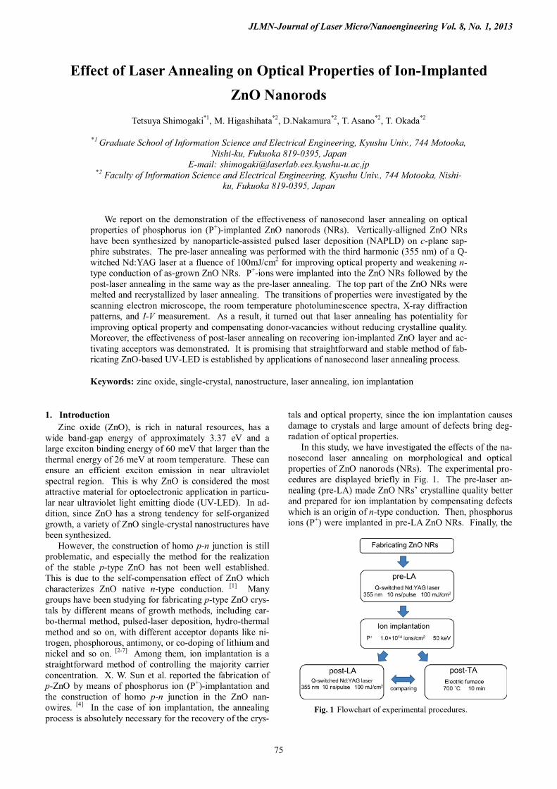
In this study, we have investigated the effects of the na-nosecond laser annealing on morphological and optical properties of ZnO nanorods (NRs). The experimental pro-cedures are displayed briefly in Fig. 1. The pre-laser an-nealing (pre-LA) made ZnO NRs’ crystalline quality better and prepared for ion implantation by compensating defects which is an origin of n-type conduction. Then, phosphorus ions (P+) were implanted in pre-LA ZnO NRs. Finally, the
Fig. 1 Flowchart of experimental procedures.
Hiromi
タイプライターテキスト
DOI:10.2961/jlmn.2013.01.0015
JLMN-Journal of Laser Micro/Nanoengineering Vol. 8, No. 1, 2013
76
post-laser annealing (post-LA) recovered the crystal struc-ture and room temperature photoluminescence (RT-PL) property of the P+-implanted ZnO NRs. In addition, it was compared with RT-PL spectrum of ZnO NRs after post-thermal annealing (post-TA) by an electric furnace. We report on the effectiveness of nanosecond laser annealing for fabricating p-type nanostructured ZnO by means of ion implantation. 2. Experiment
2.1 ZnO NRs preparation Vertically-aligned ZnO NRs used in this study were
synthesized by nano particle assisted pulsed laser deposi-tion (NAPLD). NAPLD does not require any catalysts and high-vacuum environment. Furthermore, various ZnO nanostructures can be grown on the many substrates by controlling experimental conditions. [8-11] Densely-packed ZnO NRs, which is adequate to ion implantation, was adopted in this study.
A sintered pure ZnO target placed in a vacuum chamber was ablated for 25 min with the third harmonic of a Q-switched Nd:YAG laser (Quanta-Ray, GCR-290, Spectra Physics) at 355 nm with a repetition rate of 10 Hz and a fluence of approximately 1.5 J/cm2. The pressure in the chamber and the O2 gas influx were kept at 667 Pa and 20 cm3/min, respectively. ZnO NRs were grown on thermal annealed (1000 ºC, for 120 min) c-cut sapphire substrate placed on a SiC plate heated at 700 ºC faced the ZnO target at a distance of 40 mm.
Scanning electron microscope (SEM) images of the as-grown ZnO NRs are shown in Fig. 2 (a) and (b). Figure 2 (a) and the upper right inset in Fig. 2 (a) display the view tilted by 45˚ and the top view, respectively. ZnO NRs with a diameter of approximately 500 nm are densely grown on the whole surface of substrate. In addition, the height of ZnO NRs is approximately 3 µm as shown in Fig. 2 (b).
2.2 Pre-laser annealing
The pre-LA was performed in air with the Q-switched Nd:YAG laser at 355 nm and a fluence of 100 mJ/cm2 by 10 ns/pulse. The laser beam was irradiated on the surface of ZnO NRs while the position was adjusted by precision XY stage so that the number of irradiation should be 1 pulse/location. [12]
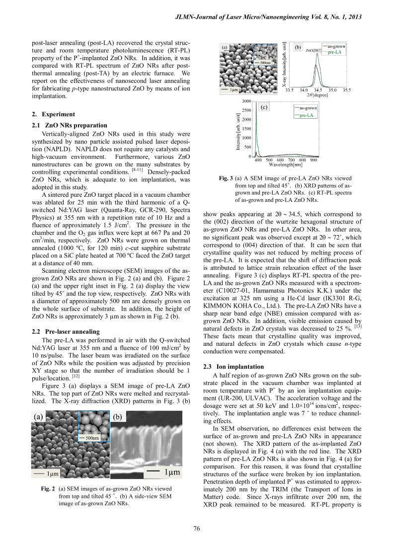
Figure 3 (a) displays a SEM image of pre-LA ZnO NRs. The top part of ZnO NRs were melted and recrystal-lized. The X-ray diffraction (XRD) patterns in Fig. 3 (b)
show peaks appearing at 2θ ∼ 34.5, which correspond to the (002) direction of the wurtzite hexagonal structure of as-grown ZnO NRs and pre-LA ZnO NRs. In other area, no significant peak was observed except at 2θ ∼ 72˚, which correspond to (004) direction of that. It can be seen that crystalline quality was not reduced by melting process of the pre-LA. It is expected that the shift of diffraction peak is attributed to lattice strain relaxation effect of the laser annealing. Figure 3 (c) displays RT-PL spectra of the pre-LA and the as-grown ZnO NRs measured with a spectrom-eter (C10027-01, Hamamatsu Photonics K.K.) under the excitation at 325 nm using a He-Cd laser (IK3301 R-G, KIMMON KOHA Co., Ltd.). The pre-LA ZnO NRs have a sharp near band edge (NBE) emission compared with as-grown ZnO NRs. In addition, visible emission caused by natural defects in ZnO crystals was decreased to 25 %. [13] These facts mean that crystalline quality was improved, and natural defects in ZnO crystals which cause n-type conduction were compensated.
2.3 Ion implantation
A half region of as-grown ZnO NRs grown on the sub-strate placed in the vacuum chamber was implanted at room temperature with P+ by an ion implantation equip-ment (UR-200, ULVAC). The acceleration voltage and the dosage were set at 50 keV and 1.0×10¹⁴ ions/cm2, respec-tively. The implantation angle was 7 ˚ to reduce channel-ing effects.
In SEM observation, no differences exist between the surface of as-grown and pre-LA ZnO NRs in appearance (not shown). The XRD pattern of the as-implanted ZnO NRs is displayed in Fig. 4 (a) with the red line. The XRD pattern of pre-LA ZnO NRs is also shown in Fig. 4 (a) for comparison. For this reason, it was found that crystalline structures of the surface were broken by ion implantation. Penetration depth of implanted P+ was estimated to approx-imately 200 nm by the TRIM (the Transport of Ions in Matter) code. Since X-rays infiltrate over 200 nm, the XRD peak remained to be measured. RT-PL property is
Fig. 2 (a) SEM images of as-grown ZnO NRs viewed from top and tilted 45 ˚. (b) A side-view SEM image of as-grown ZnO NRs.
Fig. 3 (a) A SEM image of pre-LA ZnO NRs viewed
from top and tilted 45˚. (b) XRD patterns of as-grown and pre-LA ZnO NRs. (c) RT-PL spectra of as-grown and pre-LA ZnO NRs.
JLMN-Journal of Laser Micro/Nanoengineering Vol. 8, No. 1, 2013
77
displayed in Fig. 4 (b). No luminescence was observed throughout all wavelength regions between 350 nm and 950 nm. For this reason and the fact that ZnO have a slight transmittance toward He-Cd laser, it is speculated that many defects were created in the crystal structure by ion implantation. [14]
2.4 Post-laser annealing
Next, the post-LA was performed at a fluence of 100 mJ/cm2 with the Q-switched Nd:YAG laser. The laser beam was irradiated on the surface of the P+-implanted region with a single irradiation condition by the same way as pre-LA.
Figure 5 (a) displays a SEM image of the P+-implanted ZnO NRs followed by the post-LA. As can be seen from Fig. 5 (a), top part of ZnO NRs was melted more than the one after pre-LA. The XRD pattern of the post-LA ZnO NRs is shown in Fig. 5 (b), along with that of as-implanted ZnO NRs. The crystalline quality is recovered. That is, damaged ZnO crystals were recrystallized by the post-LA. The RT-PL property of ZnO NRs after post-LA is dis-played in Fig. 5 (c), where compares it with post -TA ZnO NRs by the electric furnace as a reference. In the case of the post-LA, only NBE emission was recovered. It can be seen that defects of P+-implanted ZnO NRs are fully com-pensated by the post-LA. On the other hand, P+-implanted ZnO NRs followed by the post-thermal annealing (post-TA) had little NBE emission and strong visible emission caused by new defects in ZnO NRs. It was performed with the electric furnace at 700 ˚C for 10 min. These are at-tributed to the fact that thermal annealing is a process by
atomic motion. Accordingly, acceptors diffused excessive-ly and many Zn and O-sites remained as defects.
Consequently, defects of P+-implanted ZnO NRs were compensated insufficiently by post-TA. As stated above, the effectiveness of the laser annealing for recovering opti-cal properties of P+-implanted ZnO NRs has been demon-strated.
3. I-V measurement
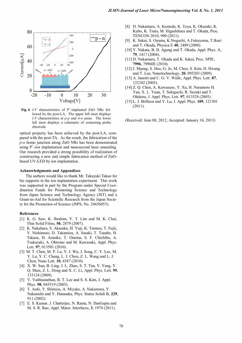
Figure 6 displays the I-V characteristics of P+-implanted ZnO NRs followed by the post-LA. This I-V characteris-tics were measured by forming ohmic contact on both p-type and n-type regions. Metal-semiconductor ohmic con-tacts were realized by using a tungsten probe and gold-deposited probe as shown in lower left inset of Fig. 6. [15] This achievement of ohmic contact is proofed by upper left inset of Fig. 6, which displays linear I-V characteristics measured between two different areas only on un-implanted ZnO NRs or on the P+-implanted ZnO NRs fol-lowed by the post-LA.
A good rectifying characteristic was observed in Fig. 6. The threshold voltage in the positive bias was approximate-ly 6 V. Since as-grown ZnO NRs have n-type conduction, the rectifying characteristic indicates that the p-type con-duction is realized in the P+-implanted ZnO NRs followed by the post-LA. In addition, linear I-V characteristics were observed in the case of post-TA (not shown).
4. Conclusion
In summary, we have demonstrated the effectiveness of the nanosecond laser annealing on ZnO NRs. The pre-LA improved optical property of as-grown ZnO NRs without reduction of their crystalline quality. We speculated that n-type conduction of as-grown ZnO NRs was reduced. The post-LA recovered the crystals and optical property of P+-implanted ZnO NRs. In particular, dramatic recovery of
Fig. 4 (a) XRD patterns of pre-LA and as-implanted
ZnO NRs. (b) RT-PL spectra of pre-LA and as-implanted ZnO NRs.
Fig. 5 (a) A SEM image of P+-implanted ZnO NRs fol-
lowed by the post-LA. (b) XRD patterns of as-implanted and post-LA ZnO NRs. (c) RT-PL spectra of as-implanted, post-LA, and post-TA ZnO NRs by the electric furnace.
JLMN-Journal of Laser Micro/Nanoengineering Vol. 8, No. 1, 2013
78
optical property has been achieved by the post-LA, com-pared with the post-TA. As the result, the fabrication of the p-n homo junction along ZnO NRs has been demonstrated using P+-ion implantation and nanosecond laser annealing. Our research provided a strong possibility of realization of constructing a new and simple fabrication method of ZnO-based UV-LED by ion implantation.
Acknowledgments and Appendixes
The authors would like to thank Mr. Takayuki Takao for his supports in the ion implantation experiment. This work was supported in part by the Program under Special Coor-dination Funds for Promoting Science and Technology from Japan Science and Technology Agency (JST) and a Grant-in-Aid for Scientific Research from the Japan Socie-ty for the Promotion of Science (JSPS, No. 24656053).
References [1] K. G. Saw, K. Ibrahim, Y. T. Lim and M. K. Chai,
Thin Solid Films, 50, 2879 (2007). [2] K. Nakahara, S. Akasaka, H. Yuji, K. Tamura, T. Fujii,
Y. Nishimoto, D. Takamizu, A. Sasaki, T. Tanabe, H. Takasu, H. Amaike, T. Onuma, S. F. Chichibu, A. Tsukazaki, A. Ohtomo and M. Kawasaki, Appl. Phys. Lett. 97, 013501 (2010).
[3] M. T. Chen, M. P. Lu, Y. J. Wu, J. Song, C. Y. Lee, M. Y. Lu, Y. C. Chang, L. J. Chou, Z. L. Wang and L. J. Chen, Nano Lett. 10, 4387 (2010).
[4] X. W. Sun, B. Ling, J. L. Zhao, S. T. Tan, Y. Yang, Y. Q. Shen, Z. L. Dong and X. C. Li, Appl. Phys. Lett. 95, 133124 (2009).
[5] V. Vaithianathan, B. T. Lee and S. S. Kim, J. Appl. Phys. 98, 043519 (2005).
[6] T. Aoki, Y. Shimizu, A. Miyake, A. Nakamura, Y. Nakanishi and Y. Hatanaka, Phys. Status Solidi B, 229, 911 (2002).
[7] E. S. Kumar, J. Chatterjee, N. Rama, N. DasGupta and M. S. R. Rao, Appl. Mater. Interfaces, 3, 1974 (2011).
[8] D. Nakamura, A. Kumeda, K. Toya, K. Okazaki, K. Kubo, K. Tsuta, M. Higashihata and T. Okada, Proc. TENCON 2010, 990 (2011).
[9] K. Sakai, S. Oyama, K.Noguchi, A.Fukuyama, T.Ikari and T. Okada, Physica E 40, 2489 (2008).
[10] Y. Nakata, B. H. Agung and T. Okada, Appl. Phys. A, 79, 1417 (2004).
[11] D. Nakamura, T. Okada and K. Sakai, Proc. SPIE, 7996, 79960E (2010).
[12] J. Maeng, S. Heo, G. Jo, M. Choe, S. Kim, H. Hwang and T. Lee, Nanotechnology, 20, 095203 (2009).
[13] A. Janotti and C. G. V. Walle, Appl. Phys. Lett. 87, 122102 (2005).
[14] Z. Q. Chen, A. Kawasuso, Y. Xu, H. Naramoto H. Yan, X. L. Yuan, T. Sekiguchi, R. Suzuki and T. Ohdaira, J. Appl. Phys. Lett. 97, 013528 (2005).
[15] L. J. Brillson and Y. Lu, J. Appl. Phys. 109, 121301 (2011).
(Received: June 08, 2012, Accepted: January 16, 2013)
Fig. 6 I-V characteristics of P+-implanted ZnO NRs fol-lowed by the post-LA. The upper left inset displays I-V characteristics at p-p and n-n areas. The lower left inset displays a schematic of contacting probe electrode.