21
El Subsistema de Memoria SISTEMES ELECTRONICS DIGITALS Enric Pastor Dept. Arquitectura de Computadors Outline Outline Cache Memory Memory: SRAM, DRAM, ROM Memory Management Units Memory Map

1
El Subsistema de Memoria
SISTEMES ELECTRONICS DIGITALS
Enric Pastor
Dept. Arquitectura de Computadors
OutlineOutline
Cache Memory
Memory: SRAM, DRAM, ROM
Memory Management Units
Memory Map

2
Caches and CPUsCaches and CPUs
CPU
cach
eco
ntro
ller cache
mainmemory
data
data
address
data
address
Cache operationCache operation
Many main memory locations are mapped onto one cache entry.
May have caches for:instructions;data;data + instructions (unified).
Memory access time is no longer deterministic.

3
TermsTerms
Cache hit: required location is in cache.
Cache miss: required location is not in cache.
Working set: set of locations used by program in a time interval.
Types of missesTypes of misses
Compulsory (cold): location has never been accessed.
Capacity: working set is too large.
Conflict: multiple locations in working set map to same cache entry.

4
Memory system performanceMemory system performance
h = cache hit rate.
tcache = cache access time, tmain = main memory access time.
Average memory access time:tav = htcache + (1-h)tmain
Multiple levels of cacheMultiple levels of cache
CPU L1 cache L2 cache

5
Multi-level cache access timeMulti-level cache access time
h1 = cache hit rate.
h2 = rate for miss on L1, hit on L2.
Average memory access time:tav = h1tL1 + (h2-h1)tL2 + (1- h2-h1)tmain
Replacement policiesReplacement policies
Replacement policy: strategy for choosing which cache entry to throw out to make room for a new memory location.
Two popular strategies:Random.Least-recently used (LRU).

6
Cache organizationsCache organizations
Fully-associative: any memory location can be stored anywhere in the cache (almost never implemented).
Direct-mapped: each memory location maps onto exactly one cache entry.
N-way set-associative: each memory location can go into one of n sets.
Cache performance benefitsCache performance benefits
Keep frequently-accessed locations in fast cache.
Cache retrieves more than one word at a time.Sequential accesses are faster after first access.

7
Direct-mapped cacheDirect-mapped cache
valid
=tag index offset
hit value
tag data1 0xabcd byte byte byte ...
byte
cache block
Write operationsWrite operations
Write-through: immediately copy write to main memory.
Write-back: write to main memory only when location is removed from cache.
8
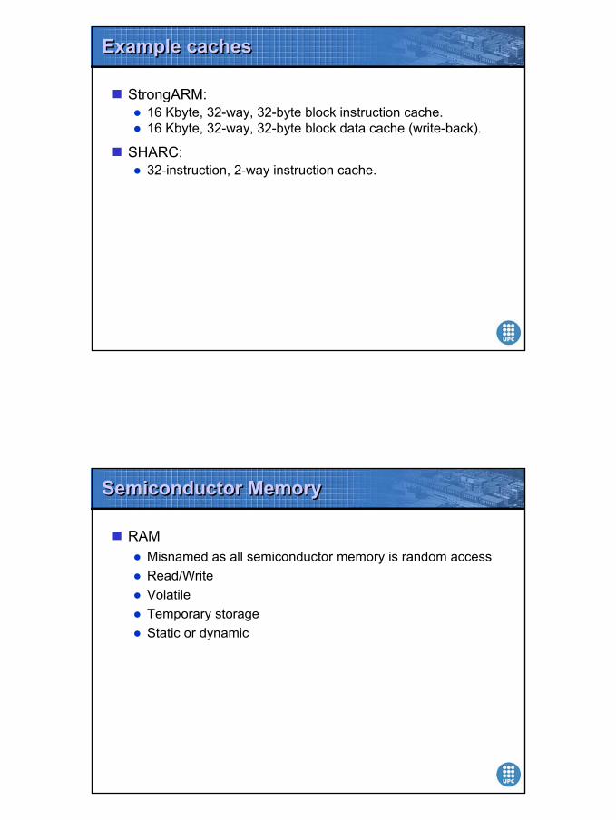
Example cachesExample caches
StrongARM:16 Kbyte, 32-way, 32-byte block instruction cache.16 Kbyte, 32-way, 32-byte block data cache (write-back).
SHARC:32-instruction, 2-way instruction cache.
Semiconductor MemorySemiconductor Memory
RAM Misnamed as all semiconductor memory is random accessRead/WriteVolatileTemporary storageStatic or dynamic

9
Dynamic RAMDynamic RAM
Bits stored as charge in capacitors
Charges leak
Need refreshing even when powered
Simpler construction
Smaller per bit
Less expensive
Need refresh circuits
Slower
Main memory
Static RAMStatic RAM
Bits stored as on/off switches
No charges to leak
No refreshing needed when powered
More complex construction
Larger per bit
More expensive
Does not need refresh circuits
Faster
Cache

10
Read Only Memory (ROM)Read Only Memory (ROM)
Permanent storage
Microprogramming (see later)
Library subroutines
Systems programs (BIOS)
Function tables
Types of ROMTypes of ROM
Written during manufactureVery expensive for small runs
Programmable (once)PROMNeeds special equipment to program
Read “mostly”Erasable Programmable (EPROM)
Erased by UVElectrically Erasable (EEPROM)
Takes much longer to write than readFlash memory
Erase whole memory electrically

11
Organisation in detailOrganisation in detail
A 16Mbit chip can be organised as 1M of 16 bit words
A bit per chip system has 16 lots of 1Mbit chip with bit 1 of each word in chip 1 and so on
A 16Mbit chip can be organised as a 2048 x 2048 x 4bit array
Reduces number of address pinsMultiplex row address and column address11 pins to address (211=2048)Adding one more pin doubles range of values so x4 capacity
RefreshingRefreshing
Refresh circuit included on chip
Disable chip
Count through rows
Read & Write back
Takes time
Slows down apparent performance

12
Typical 16 Mb DRAM (4M x 4)Typical 16 Mb DRAM (4M x 4)
Chip PackagingChip Packaging

13
Module OrganisationModule Organisation
Newer RAM TechnologyNewer RAM Technology
Basic DRAM same since first RAM chips
Enhanced DRAMContains small SRAM as wellSRAM holds last line read (c.f. Cache!)
Cache DRAMLarger SRAM componentUse as cache or serial buffer

14
Newer RAM TechnologyNewer RAM Technology
Synchronous DRAM (SDRAM)Currently on DIMMsAccess is synchronized with an external clockAddress is presented to RAMRAM finds data (CPU waits in conventional DRAM)Since SDRAM moves data in time with system clock, CPU knows when data will be readyCPU does not have to wait, it can do something elseBurst mode allows SDRAM to set up stream of data and fire it out in block
SDRAM StructureSDRAM Structure
15
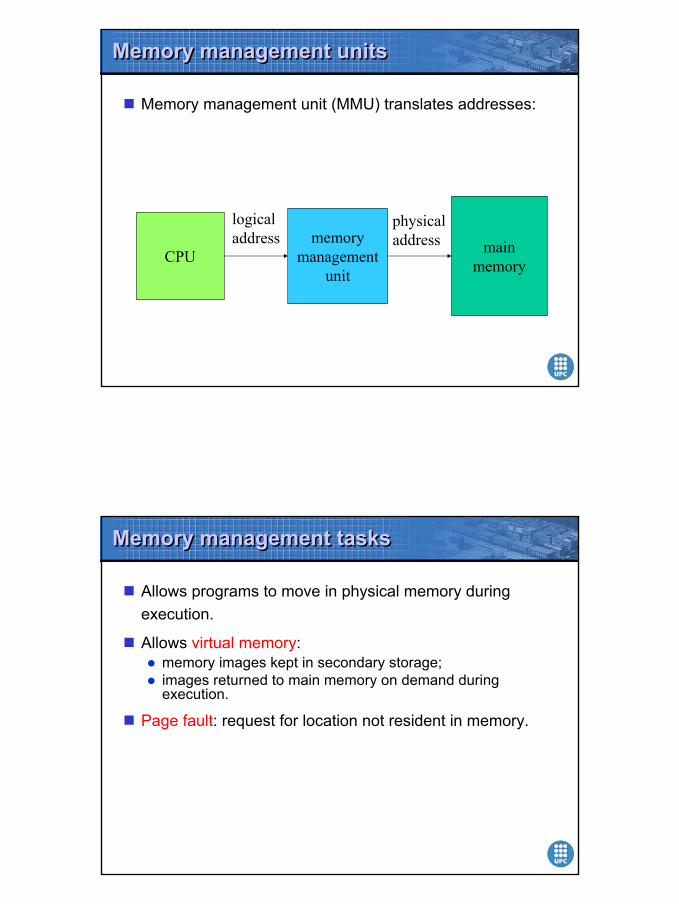
Memory management unitsMemory management units
Memory management unit (MMU) translates addresses:
CPU mainmemory
memorymanagement
unit
logicaladdress
physicaladdress
Memory management tasksMemory management tasks
Allows programs to move in physical memory during execution.
Allows virtual memory:memory images kept in secondary storage;images returned to main memory on demand during execution.
Page fault: request for location not resident in memory.

16
Address translationAddress translation
Requires some sort of register/table to allow arbitrary mappings of logical to physical addresses.
Two basic schemes:segmented;paged.
Segmentation and paging can be combined (x86).
Segments and pagesSegments and pages
memory
segment 1
segment 2
page 1page 2
17
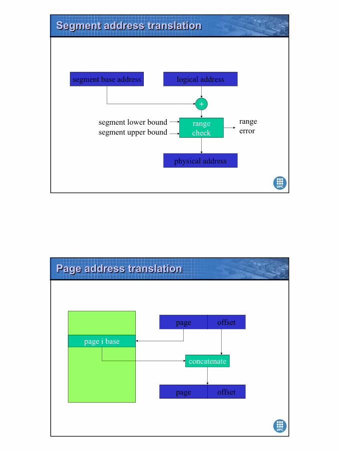
Segment address translationSegment address translation
segment base address logical address
rangecheck
physical address
+
rangeerror
segment lower boundsegment upper bound
Page address translationPage address translation
page offset
page offset
page i base
concatenate

18
Page table organizationsPage table organizations
flat tree
page descriptor
pagedescriptor
Caching address translationsCaching address translations
Large translation tables require main memory access.
TLB: cache for address translation.Typically small.

19
ARM memory managementARM memory management
Memory region types:section: 1 Mbyte block;large page: 64 kbytes;small page: 4 kbytes.
An address is marked as section-mapped or page-mapped.
Two-level translation scheme.
ARM address translationARM address translation
offset1st index 2nd index
physical address
Translation tablebase register
1st level tabledescriptor
2nd level tabledescriptor
concatenate
concatenate
20
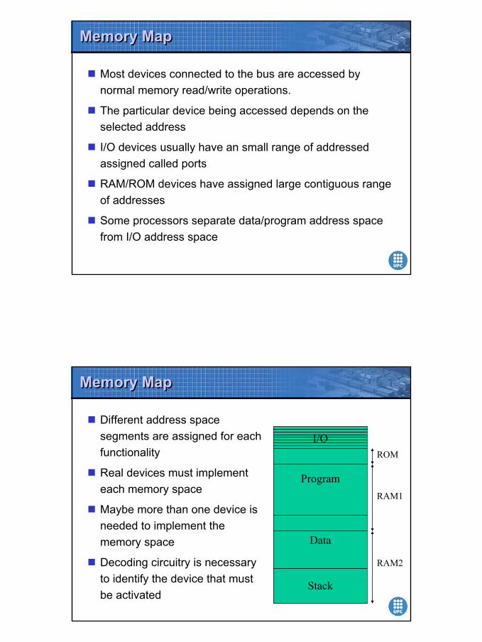
Memory MapMemory Map
Most devices connected to the bus are accessed by normal memory read/write operations.
The particular device being accessed depends on the selected address
I/O devices usually have an small range of addressed assigned called ports
RAM/ROM devices have assigned large contiguous range of addresses
Some processors separate data/program address space from I/O address space
Memory MapMemory Map
Different address space segments are assigned for each functionality
Real devices must implement each memory space
Maybe more than one device is needed to implement the memory space
Decoding circuitry is necessary to identify the device that must be activated
I/O
Program
Data
Stack
ROM
RAM1
RAM2

21
Memory MapMemory Map
System Bus
ROMRAM1 RAM2 I/O I/OI/O
DecodingLogic
BusAddress
Chip SelectSignals
CS CSCSCSCS CS
Only one Chip Select (CS) bit is activated for each address placed on the bus


![Curriculo Subsistema de Educacion Regular[1]](https://static.documents.pub/doc/80x56/563dbb5e550346aa9aac8c39/curriculo-subsistema-de-educacion-regular1.jpg)