ELEC 7770 Advanced VLSI Design Spring 2014 Constraint Graph and Retiming Solution. Vishwani D. Agrawal James J. Danaher Professor ECE Department, Auburn University Auburn, AL 36849 [email protected] http://www.eng.auburn.edu/~vagrawal/COURSE/E7770_Spr14/course.html. Retiming Theorem. - PowerPoint PPT Presentation
40
Spring 2014, Feb 14 . . . Spring 2014, Feb 14 . . . ELEC 7770: Advanced VLSI Design ELEC 7770: Advanced VLSI Design (Agrawal) (Agrawal) 1 ELEC 7770 ELEC 7770 Advanced VLSI Design Advanced VLSI Design Spring 2014 Spring 2014 Constraint Graph and Retiming Constraint Graph and Retiming Solution Solution Vishwani D. Agrawal Vishwani D. Agrawal James J. Danaher Professor James J. Danaher Professor ECE Department, Auburn University ECE Department, Auburn University Auburn, AL 36849 Auburn, AL 36849 [email protected]http://www.eng.auburn.edu/~vagrawal/COURSE/E7770_Spr14/ http://www.eng.auburn.edu/~vagrawal/COURSE/E7770_Spr14/ course.html course.html
Transcript
Spring 2014, Feb 14 . . .Spring 2014, Feb 14 . . . ELEC 7770: Advanced VLSI Design (Agrawal)ELEC 7770: Advanced VLSI Design (Agrawal) 11
Spring 2014, Feb 14 . . .Spring 2014, Feb 14 . . . ELEC 7770: Advanced VLSI Design (Agrawal)ELEC 7770: Advanced VLSI Design (Agrawal) 22
Retiming TheoremRetiming Theorem Given a network G(V, E, W) and a cycle time T, Given a network G(V, E, W) and a cycle time T,
(r1, . . . ) is a feasible retiming if and only if:(r1, . . . ) is a feasible retiming if and only if: ri – rj ri – rj ≤ wij≤ wij for all edges (vi,vj) for all edges (vi,vj) εε E E ri – rj ≤ W(vi,vj) – 1 ri – rj ≤ W(vi,vj) – 1 for all node-pairs vi, vj such thatfor all node-pairs vi, vj such that
D(vi,vj) D(vi,vj) > T> T
Where,Where,
W(vi,vj) is the minimum weight path between vi and vjW(vi,vj) is the minimum weight path between vi and vj
D(vi,vj) is the maximum delay among all minimum D(vi,vj) is the maximum delay among all minimum weight paths between vi and vjweight paths between vi and vj
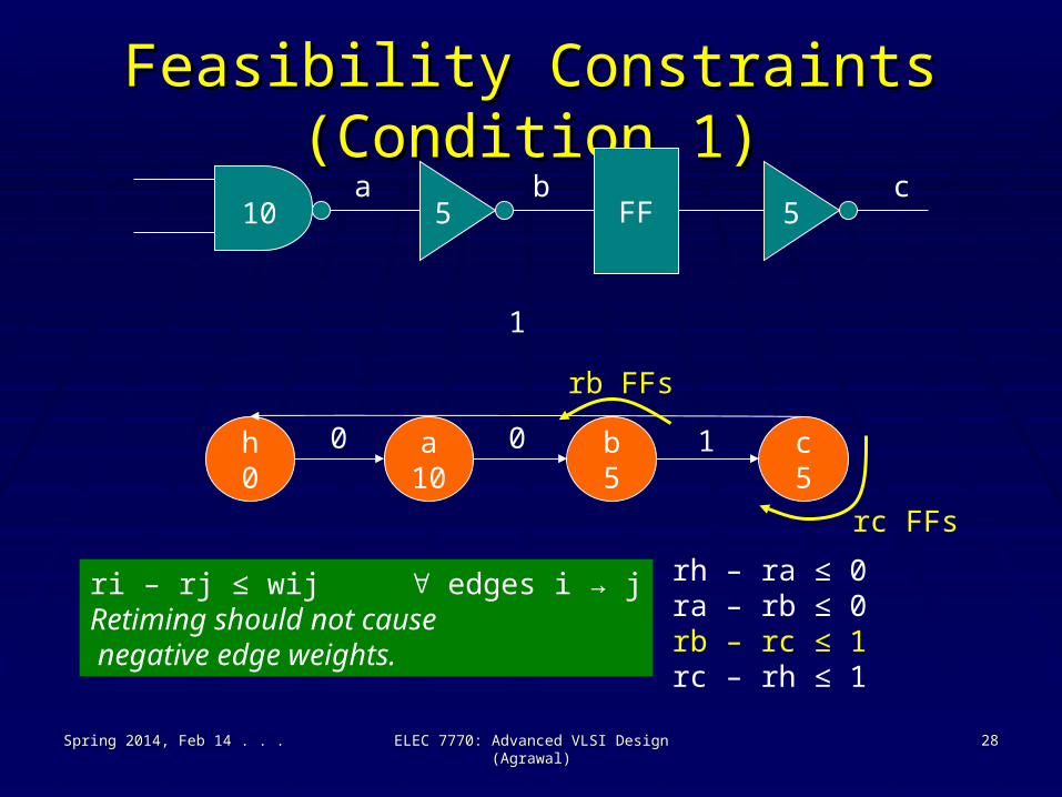
Retiming Theorem ExplainedRetiming Theorem Explained Condition 1, ri – rj Condition 1, ri – rj ≤ wij, is related to edge weight:≤ wij, is related to edge weight:
Original circuit is feasible Original circuit is feasible original weight wij is positive original weight wij is positive Originally, ri = rj = 0Originally, ri = rj = 0 Retiming, rj flip-flops added to eij, ri flip-flops removed Retiming, rj flip-flops added to eij, ri flip-flops removed
from eij, net reduction ri – rj must be less than wij to leave from eij, net reduction ri – rj must be less than wij to leave the retimed weight of eij positive.the retimed weight of eij positive.
Condition 2, ri – rj ≤ W(vi,vj) – 1 is related to path Condition 2, ri – rj ≤ W(vi,vj) – 1 is related to path delays between node pairs being less than clock delays between node pairs being less than clock period T whenever path weight is 0.period T whenever path weight is 0.
Spring 2014, Feb 14 . . .Spring 2014, Feb 14 . . . ELEC 7770: Advanced VLSI Design (Agrawal)ELEC 7770: Advanced VLSI Design (Agrawal) 33
Examine Condition 2Examine Condition 2
Spring 2014, Feb 14 . . .Spring 2014, Feb 14 . . . ELEC 7770: Advanced VLSI Design (Agrawal)ELEC 7770: Advanced VLSI Design (Agrawal) 44
vi vj
ri rj
W1, D1
W2, D2
W3, D3
W1 = W2 < W3, W(vi, vj) = W1 = W2, minimum weight among pathsD1 > D2, therefore D(vi, vj) = D1, maximum delay of a minimum weigh pathIf D1 ≤ T, there is no requirement on ri, rjIf D1 > T, Retimed weight W1’ = W1 – ri + rj ≥ 1 (at least 1 FF on path)
or ri – rj ≤ W1 – 1
Spring 2014, Feb 14 . . .Spring 2014, Feb 14 . . . ELEC 7770: Advanced VLSI Design (Agrawal)ELEC 7770: Advanced VLSI Design (Agrawal) 55
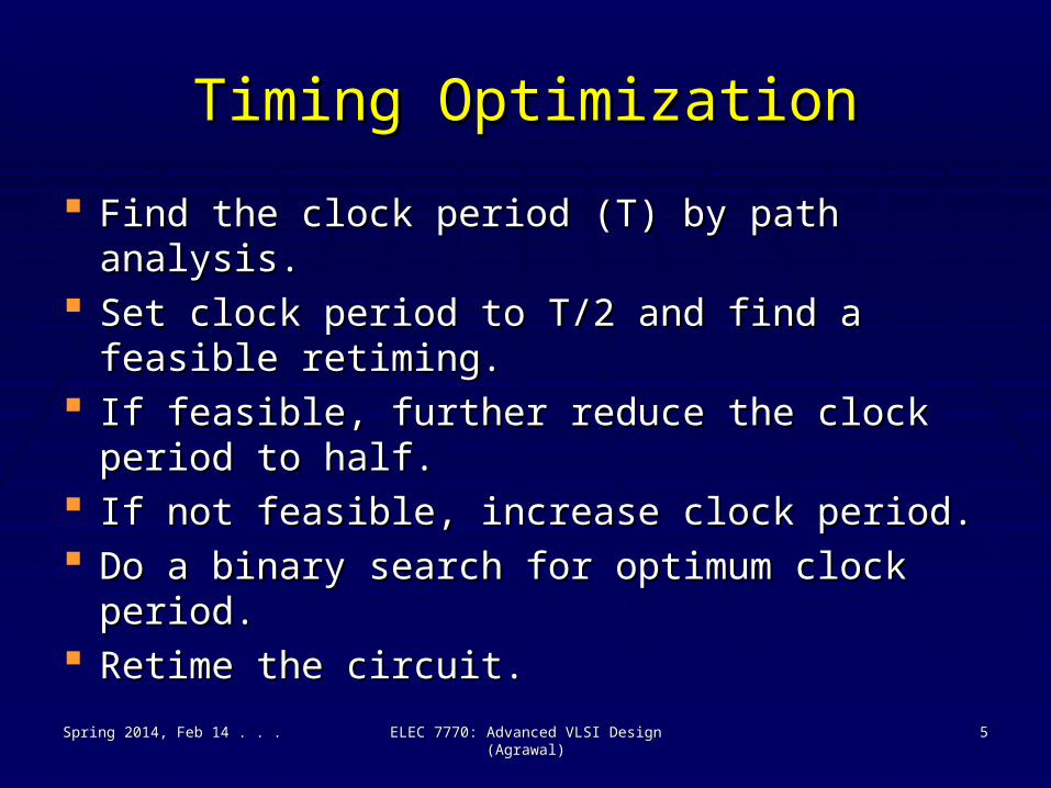
Timing OptimizationTiming Optimization
Find the clock period (T) by path analysis.Find the clock period (T) by path analysis. Set clock period to T/2 and find a feasible Set clock period to T/2 and find a feasible
retiming.retiming. If feasible, further reduce the clock period to If feasible, further reduce the clock period to
half.half. If not feasible, increase clock period.If not feasible, increase clock period. Do a binary search for optimum clock period.Do a binary search for optimum clock period. Retime the circuit.Retime the circuit.
Spring 2014, Feb 14 . . .Spring 2014, Feb 14 . . . ELEC 7770: Advanced VLSI Design (Agrawal)ELEC 7770: Advanced VLSI Design (Agrawal) 66
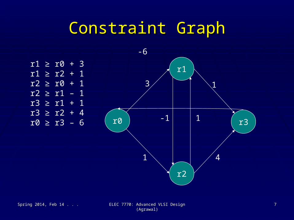
Representing a ConstraintRepresenting a Constraint
ri – rj ≤ wij or rj ≥ ri – wij
rj ri– wij
Spring 2014, Feb 14 . . .Spring 2014, Feb 14 . . . ELEC 7770: Advanced VLSI Design (Agrawal)ELEC 7770: Advanced VLSI Design (Agrawal) 77
Spring 2014, Feb 14 . . .Spring 2014, Feb 14 . . . ELEC 7770: Advanced VLSI Design (Agrawal)ELEC 7770: Advanced VLSI Design (Agrawal) 88
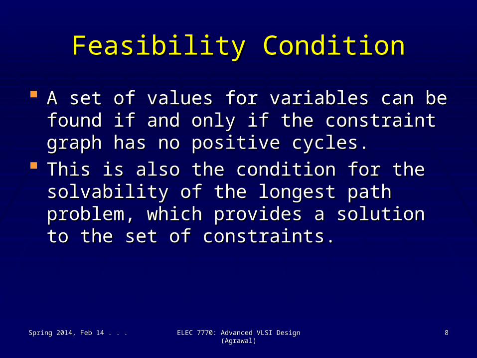
Feasibility ConditionFeasibility Condition
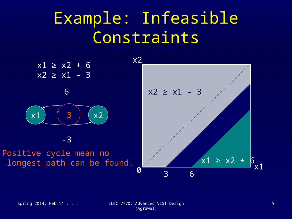
A set of values for variables can be found if and A set of values for variables can be found if and only if the constraint graph has no positive only if the constraint graph has no positive cycles.cycles.
This is also the condition for the solvability of the This is also the condition for the solvability of the longest path problem, which provides a solution longest path problem, which provides a solution to the set of constraints.to the set of constraints.
Spring 2014, Feb 14 . . .Spring 2014, Feb 14 . . . ELEC 7770: Advanced VLSI Design (Agrawal)ELEC 7770: Advanced VLSI Design (Agrawal) 99
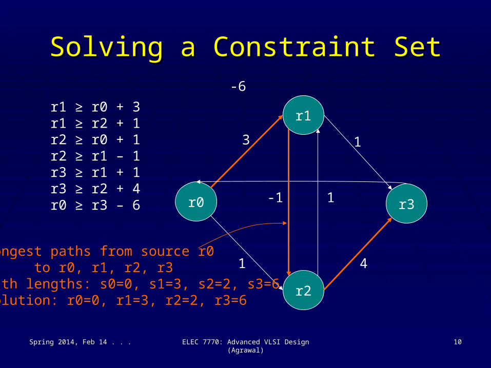
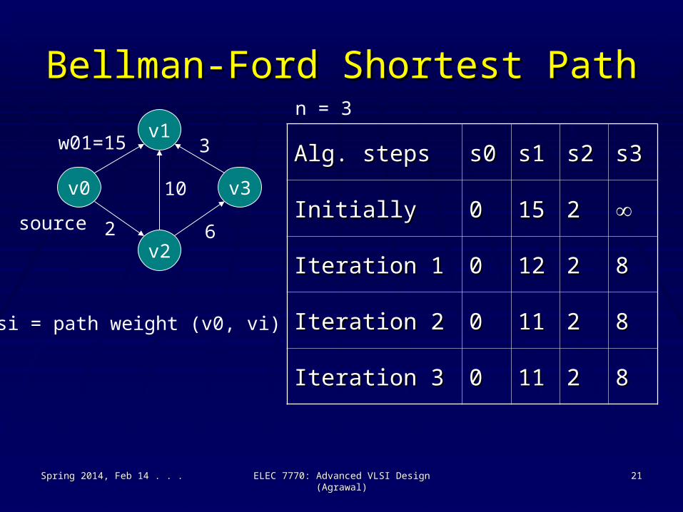
Longest paths from source r0 to r0, r1, r2, r3Path lengths: s0=0, s1=3, s2=2, s3=6Solution: r0=0, r1=3, r2=2, r3=6
Spring 2014, Feb 14 . . .Spring 2014, Feb 14 . . . ELEC 7770: Advanced VLSI Design (Agrawal)ELEC 7770: Advanced VLSI Design (Agrawal) 1111
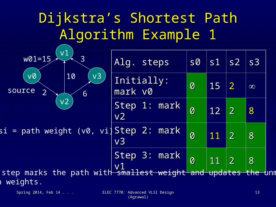
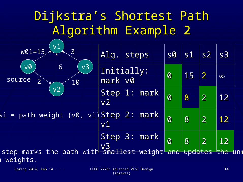
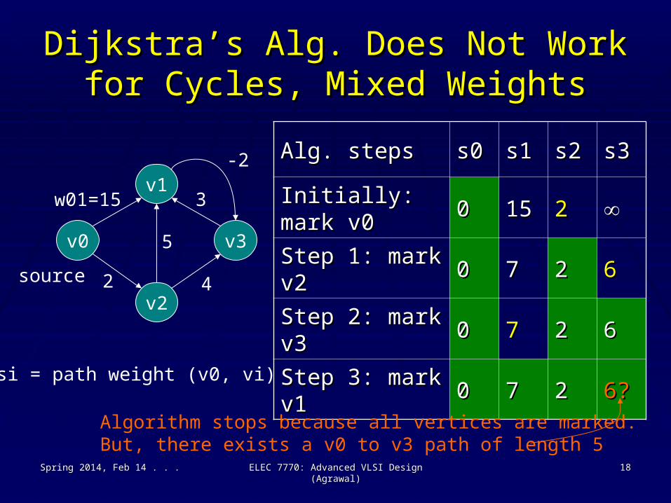
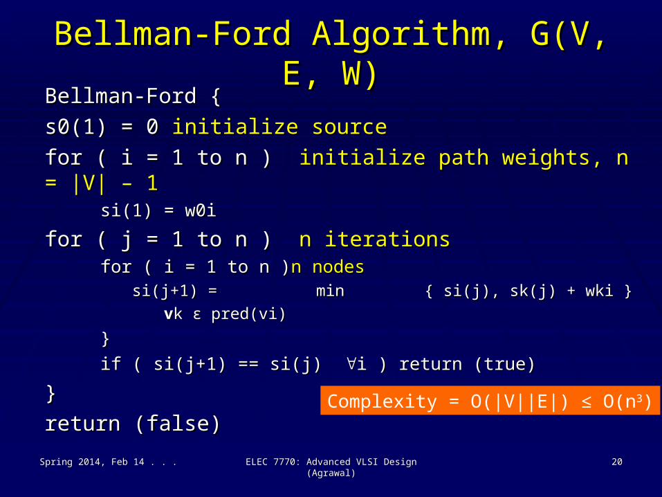
The General Path ProblemThe General Path Problem Find the shortest (or longest) path in a graph Find the shortest (or longest) path in a graph
from a source vertex to all other vertices.from a source vertex to all other vertices. Graph has vertices and directed edges:Graph has vertices and directed edges:
Edge weights can be positive or negativeEdge weights can be positive or negative Graph can be cyclicGraph can be cyclic Single source vertex – a vertex with 0 in-degree (not Single source vertex – a vertex with 0 in-degree (not
a necessary condition)a necessary condition)
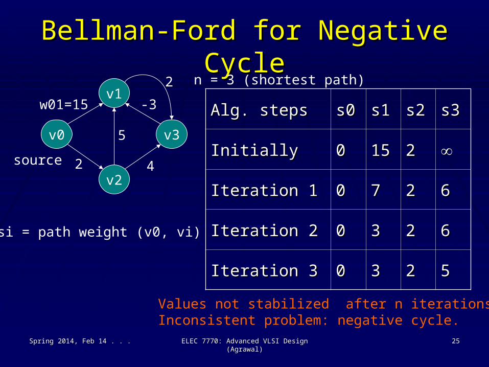
Inconsistent problemsInconsistent problems Negative weight cycles for shortest pathNegative weight cycles for shortest path Positive weight cycles for longest pathPositive weight cycles for longest path
Spring 2014, Feb 14 . . .Spring 2014, Feb 14 . . . ELEC 7770: Advanced VLSI Design (Agrawal)ELEC 7770: Advanced VLSI Design (Agrawal) 1212
A. Aho, J. Hopcroft and J. Ullman, A. Aho, J. Hopcroft and J. Ullman, Data Structures and Data Structures and AlgorithmsAlgorithms, Reading, Massachusetts: Addison-Wesley, 1983., Reading, Massachusetts: Addison-Wesley, 1983.
T. Cormen, C. Leiserson and R. Rivest, T. Cormen, C. Leiserson and R. Rivest, Introduction to Introduction to AlgorithmsAlgorithms, New York: McGraw-Hill, 1990., New York: McGraw-Hill, 1990.
Spring 2014, Feb 14 . . .Spring 2014, Feb 14 . . . ELEC 7770: Advanced VLSI Design (Agrawal)ELEC 7770: Advanced VLSI Design (Agrawal) 1313
Observation: Constraint graph has the same structure as the original retiming graph, with signs of weights reversed. Vertex labels are the retiming integer variables.
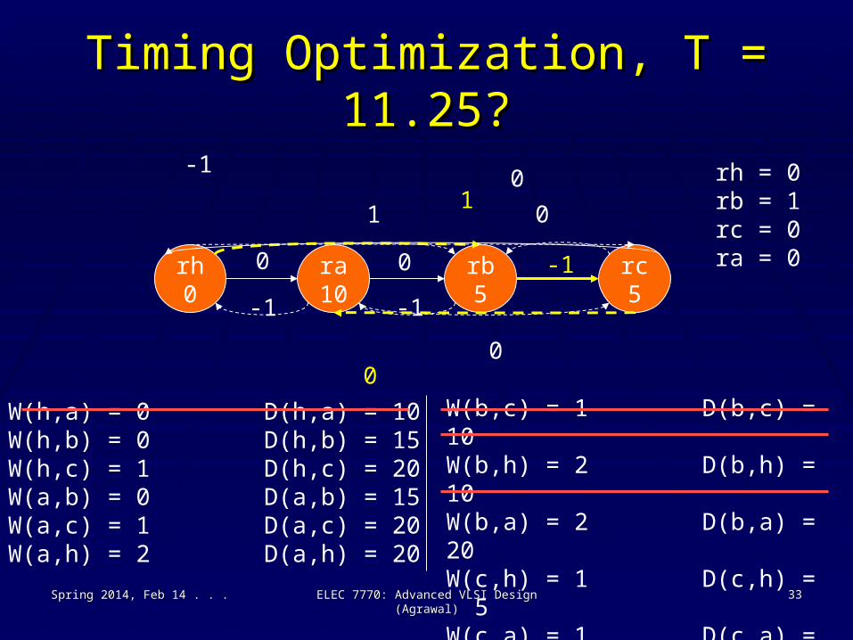
Spring 2014, Feb 14 . . .Spring 2014, Feb 14 . . . ELEC 7770: Advanced VLSI Design (Agrawal)ELEC 7770: Advanced VLSI Design (Agrawal) 3030
Max Delay for Min Weight PathsMax Delay for Min Weight Paths
C. E. Leiserson, F. Rose and J. B. Saxe, “Optimizing C. E. Leiserson, F. Rose and J. B. Saxe, “Optimizing Synchronous Circuits by Retiming,” Synchronous Circuits by Retiming,” Proc. 3Proc. 3rdrd Caltech Caltech Conf. on VLSIConf. on VLSI, 1983, pp. 87-116., 1983, pp. 87-116.
C. E. Leiserson and J. B. Saxe, “Retiming Synchronous C. E. Leiserson and J. B. Saxe, “Retiming Synchronous Circuitry,” Circuitry,” AlgorithmicaAlgorithmica, vol. 6, pp. 5-35, 1991., vol. 6, pp. 5-35, 1991.
G. De Micheli, G. De Micheli, Synthesis and Optimization of Digital Synthesis and Optimization of Digital CircuitsCircuits, New York: McGraw-Hill, 1994, Section 9.3.1., New York: McGraw-Hill, 1994, Section 9.3.1.
N. Maheshwari and S. S. Sapatnekar, N. Maheshwari and S. S. Sapatnekar, Timing Analysis Timing Analysis and Optimization of Sequential Circuitsand Optimization of Sequential Circuits, Boston: , Boston: Springer, 1999, Chapter 4.Springer, 1999, Chapter 4.
Spring 2014, Feb 14 . . .Spring 2014, Feb 14 . . . ELEC 7770: Advanced VLSI Design (Agrawal)ELEC 7770: Advanced VLSI Design (Agrawal) 4040