ELEC3242 Communications Engineering Laboratory 1 ---- Frequency Shift Keying (FSK) 1) Frequency Shift Keying Objectives To appreciate the principle of frequency shift keying and its relationship to analogue frequency modulation To generate a two-level (binary) frequency shift keyed signal and investigate the spectrum and bandwidth associated with it To investigate the demodulation of an FSK signal To understand the concept of Minimum shift keying’ and its use to limit the bandwidth of an FSK signal To generate and subsequently demodulate a minimum shift keyed signal To appreciate the concept of multi-level FSK (MFSK) and to generate 4, 8 and 16 level MFSK signals To investigate the spectrum occupied by an MFSK signal and its relationship to symbol rate 2) Bessel Function and FM Modulation The equation of a sinusoidal voltage waveform is given by: where: v is the instantaneous voltage, v = V max .sin(ωt+Ø) V max is the maximum voltage amplitude, ω is the angular frequency, Ø is the phase.
Transcript
ELEC3242 Communications Engineering Laboratory 1 ---- Frequency Shift Keying (FSK)
1) Frequency Shift Keying
Objectives
To appreciate the principle of frequency shift keying and its relationship to analogue frequency modulation
To generate a two-level (binary) frequency shift keyed signal and investigate the
spectrum and bandwidth associated with it
To investigate the demodulation of an FSK signal
To understand the concept of Minimum shift keying’ and its use to limit the bandwidth of an FSK signal
To generate and subsequently demodulate a minimum shift keyed signal
To appreciate the concept of multi-level FSK (MFSK) and to generate 4, 8 and 16 level MFSK signals
To investigate the spectrum occupied by an MFSK signal and its relationship to
symbol rate
2) Bessel Function and FM
Modulation The equation of a sinusoidal voltage waveform is given by:
where:
v is the instantaneous voltage,
v = Vmax.sin(ωt+Ø)
Vmax is the maximum voltage amplitude,
ω is the angular frequency,
Ø is the phase.
A steady voltage corresponding to the above equation conveys little information.
To convey information the waveform must be made to vary so that the variations represent the information. This process is called modulation.
Any of these may be varied to convey information.
Frequency Modulation
Frequency modulation uses variations in frequency to convey information.
The wave whose frequency is being varied is called the carrier wave. The signal doing the variation is called the modulating signal.
For simplicity, suppose both carrier wave and modulating signal are sinusoidal; ie:
(c denotes carrier) and
(m denotes modulation)
What is Frequency?
vc = Vc sin ωc t
vm = Vm cos ωm t
If the frequency is varying, how can it be defined?
You can no longer count the number of cycles over a longish interval to determine the cycles per second. Instead, frequency is defined as the rate of change of phase.
This is consistent with the simple definition because, at a constant (angular) frequency ω
radians/second, the phase is changing at ω radians per second, which is ω/2π cycles per
second.
Since the instantaneous frequency can only be defined by reference to the phase, the phase must be examined in order to arrive at an expression for the frequency-modulated signal.
Phase of the FM Signal
For the unmodulated carrier vc = Vc sin ωc t, the phase is:
φ = ωc t
The modulating signal varies the carrier frequency, ωc, so that its frequency takes the form:
ω = ωc + D cos ωm t
(where D denotes the peak value of the deviation).
It is related to the amplitude of the modulating signal vm by the 'frequency slope' of the frequency modulator (VCO), say k radians/s per V.
The peak value of vm produces deviation D, so:
D = k Vm
The total phase change undergone at time t is found by integrating the angular frequency.
It is
φ = ∫(ωc + D cos ωm t) dt
= ωct + (D/ωm) sin ωm t
(If you are not familiar with integration you will have to take this result on trust).
So the FM signal can be expressed as:
Vc sin [ωct + (D/ωm) sin ωm t]
Modulation Index
In the expression for the FM signal:
Vc sin [ωc t + (D/ωm) sin ωm t]
the coefficient D/ωm turns out to be quite important and is given the name modulation
index.
It is often represented by the Greek letter beta, β.
So we may write the FM signal as:
vc = Vc sin (ωct + βsin ωm) t
where β is the modulation index D/ωm.
In this expression, the factor sin (ωct + βsin ωm)t (let us call it F) is of the form sin(a + b),
which can be expanded to sin a cos b + cos a sin b.
Applying this expansion to F, we get:
F = sin ωct cos(sin βωm) t + cos ωct sin (sin βωm) t
FM Sidebands
These complicated functions can be expanded, using mathematics too elaborate to explain here, into a series of terms like this:
F = J0(β) sin ωct+ J1(β) [ sin (ωc + ωm)t - sin (ωc - ωm)t ]
+ J2(β) [ sin (ωc + 2ωm)t - sin (ωc - 2ωm)t ]
+ J3(β) [ sin (ωc + 3ωm)t - sin (ωc - 3ωm)t ]
+ J4(β) [ sin (ωc + 4ωm)t - sin (ωc - 4ωm)t ]
+ ...
where J0(β), J1(β), J2(β) etc are constants whose values depend only on β. They are
called Bessel Functions.
There is an infinite series of these functions, and so an infinite number of FM sidebands.
But, in practice the values of the Bessel functions become very small as the series goes
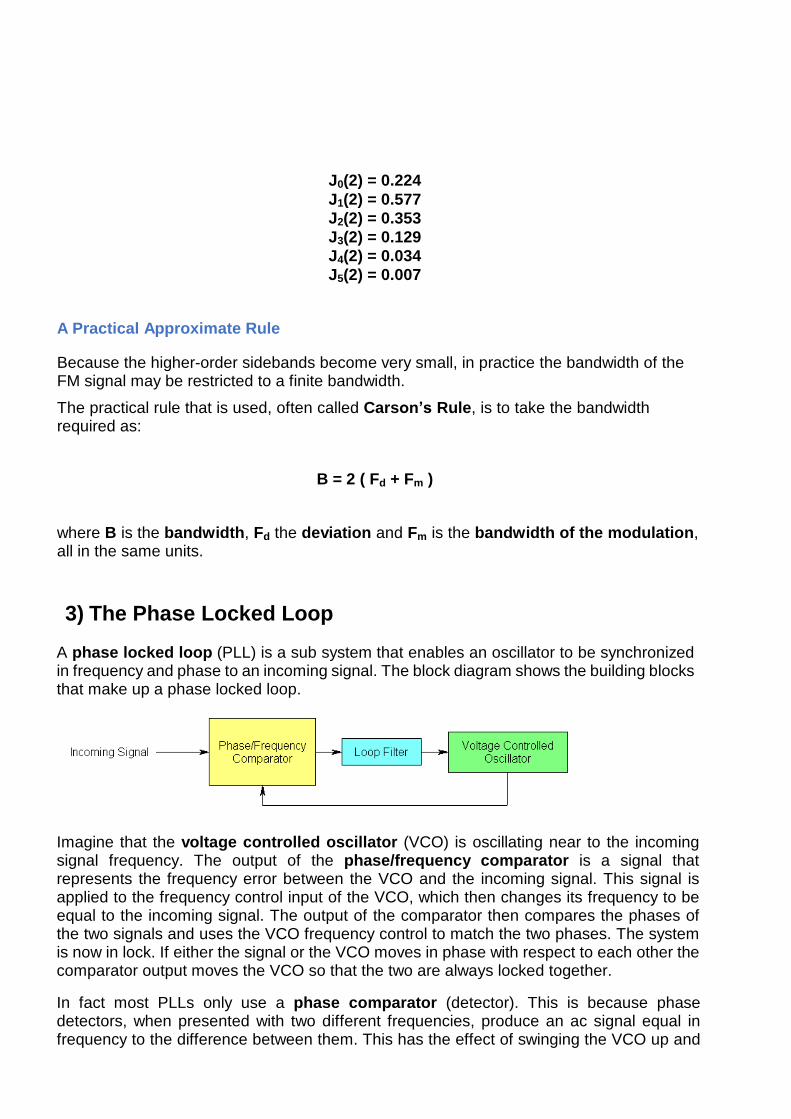
Because the higher-order sidebands become very small, in practice the bandwidth of the FM signal may be restricted to a finite bandwidth.
The practical rule that is used, often called Carson’s Rule, is to take the bandwidth required as:
B = 2 ( Fd + Fm )
where B is the bandwidth, Fd the deviation and Fm is the bandwidth of the modulation, all in the same units.
3) The Phase Locked Loop
A phase locked loop (PLL) is a sub system that enables an oscillator to be synchronized in frequency and phase to an incoming signal. The block diagram shows the building blocks that make up a phase locked loop.
Imagine that the voltage controlled oscillator (VCO) is oscillating near to the incoming signal frequency. The output of the phase/frequency comparator is a signal that represents the frequency error between the VCO and the incoming signal. This signal is applied to the frequency control input of the VCO, which then changes its frequency to be equal to the incoming signal. The output of the comparator then compares the phases of the two signals and uses the VCO frequency control to match the two phases. The system is now in lock. If either the signal or the VCO moves in phase with respect to each other the comparator output moves the VCO so that the two are always locked together.
In fact most PLLs only use a phase comparator (detector). This is because phase detectors, when presented with two different frequencies, produce an ac signal equal in frequency to the difference between them. This has the effect of swinging the VCO up and
down in frequency and, as it passes the signal frequency, the loop locks.
Loop Stability
One of the problems that will almost certainly arise, unless steps are taken to stop it, is instability. The loop relies on the system operating with negative feedback, i.e. if the VCO moves, the polarity of the control signal brings it back. This is easily done when the system is operating at, or near to, dc. However, a problem arises if you consider the loop moving in response to a fast changing frequency. The control signal will contain an ac component. All systems are subject to delays and phase shifts, which become more significant at higher frequencies. Remembering that 180 degrees phase shift is equivalent to inverting a signal, inevitably there is going to be a frequency at which the phase shift round the loop is enough to cause the polarity to reverse and positive feedback will be applied. This results in the system oscillating back and forth at the frequency which produces the positive feedback.
There is another subtle problem that results in the design of a PLL system being more difficult then you might imagine. Remember that we are using the frequency of an oscillator to control its phase. Now phase is the integral of frequency and so there is already a 90 degree shift caused by the VCO. This means that there only has to be another 90 degrees of phase shift before instability, not 180° as you might have thought.
The same problem occurs, for example, in a mechanical position control system that uses speed control, because position is the integral of speed. The phase lock loop is a control system and exactly the same mathematics can be used to describe a PLL as is used to describe a position control servo.
Of course, instability can only occur if there is enough gain in the loop at the problem frequency. This is where the loop filter can solve the problem, as it reduces gain at higher frequencies while maintaining control over phase. There will be a frequency that the loop filter produces 90 degrees of phase shift, but the gain will be low and so instability will not arise. The critical frequency is when the overall loop gain is 1 and the overall added phase shift must be less than 90 degrees at this point. The amount by which it is less is called phase margin and, in practice, should be about 45 degrees for good stable performance. The design of the loop filter is not simple and has to be done knowing all the gains and phase shifts in the system.
Many phase comparators produce a control signal that contains a significant amount of high frequency energy but this is not normally a problem as it is removed by the loop filter.
In PLLs that use phase only comparators, the bandwidth of the loop filter also determines the range over which the loop will lock on, or ‘capture’, a signal as the comparator only generates an ac signal off lock. The range over which the loop will capture a signal is called its capture range. The range over which the loop will remain locked, once lock is achieved, is called the lock range. The time to achieve lock can be important and is referred to as lock time.
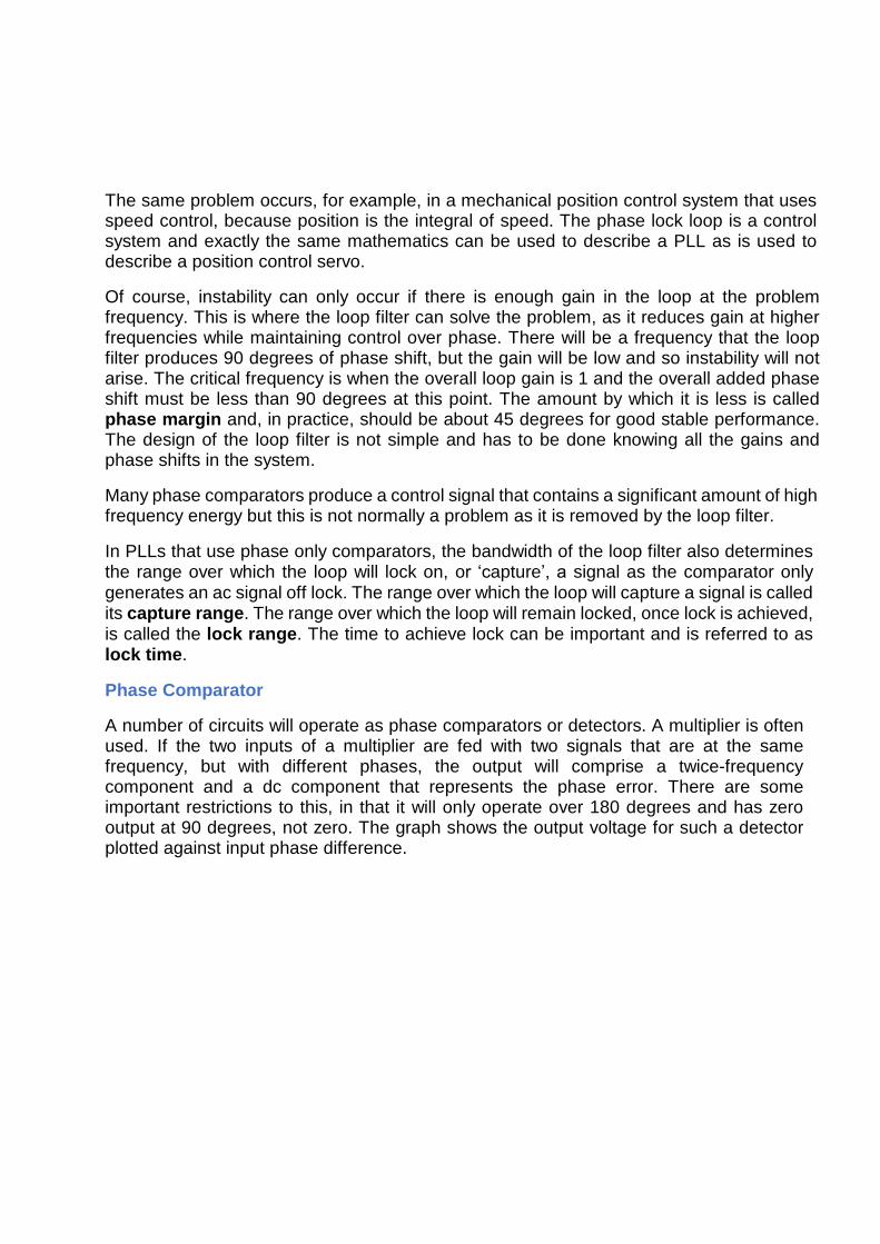
Phase Comparator
A number of circuits will operate as phase comparators or detectors. A multiplier is often used. If the two inputs of a multiplier are fed with two signals that are at the same frequency, but with different phases, the output will comprise a twice-frequency component and a dc component that represents the phase error. There are some important restrictions to this, in that it will only operate over 180 degrees and has zero output at 90 degrees, not zero. The graph shows the output voltage for such a detector plotted against input phase difference.
This shows that the output repeats for 180° to 360°, albeit in the other polarity.
This phase range problem is not significant as, in a properly operating loop, the gain is such that only a small error has to occur before the VCO is corrected.
There are other types of comparator. The logic function exclusive OR is exactly the same in action as the multiplier and is often used in digital circuits. More complex digital circuits have advantages, such as: acting as frequency comparators as well as phase comparators; operating over 360 degrees; and having less ac signal component in the output. Most of these are based on circuits using D type flip-flops. These D type comparators have the disadvantage of making the loop much less tolerant of noise in the signal. They are used in applications such as frequency synthesizers, while the multipliers and OR gates are used in applications such as demodulators or carrier reference recovery.
The design of PLLs is a complex compromise of performance parameters, the relative importance of each performance parameter depends, to a large extent, on the application.
Applications
Many phase lock loops are used to recover some sort of constant frequency component to provide a reference for a demodulator.
Another very common application is in frequency synthesizers, where an oscillator is frequency divided to some low frequency and a PLL locks it to an external reference. By changing the divider ratio, different frequencies that are all multiples of the reference frequency can be generated or ‘synthesised’.
The PLL can also be used to demodulate FM as, when locked to the FM signal, the VCO tracks the frequency modulation. Therefore the control signal to the VCO contains the modulation, plus a dc component. This dc component can easily be removed using a high pass filter. In this case the loop filter bandwidth must be high enough to pass the modulation or the VCO will not be able to follow and the loop will come out of lock. In most
cases the output is passed through a post detection filter, which will remove any remaining high frequency components but, because it is outside the loop, will not affect loop stability.
4) Inter-symbol Interference
Inter-symbol interference is a particular type of distortion applicable to digital signals. It simply refers to the fact that the present symbol may be distorted by the values of the symbols on either side of it.
For example, if a post detection filter had insufficient bandwidth and the signal did not have time to reach its maximum output during a “1” symbol, if the previous symbol was zero, then this would be regarded as inter-symbol interference.
More subtle problems may occur if there are reflections in a cable, or on radio signals, causing energy from other symbol periods to arrive at the same time.
All communication systems use filtering to maximize the signal-to-noise ratio or prevent other signals causing interference. Any filtering will cause some inter-symbol interference and it is necessary to find the right compromise between too little filtering and too much distortion. Some systems, such as GMSK (Gaussian Minimum Shift Keying), are designed to tolerate significant distortion, in order to reduce their occupied bandwidth.
5) Symbol Rate and Bit Rate
The concepts of symbols, bits, symbol rate and bit rate are important terms in digital
communications.
The concept of a bit (a binary digit) should be familiar as a one or zero in a binary data stream. The
bit rate is simply the rate at which the bits change. For example, imagine a system that digitized an
audio signal at 32k samples per second, each sample being digitized at 256 possible levels. This
means each sample is an 8 bit word. In order to send this stream over a simple link it would have to
be turned into serial data. This means the serial data stream would run at 32k x 8 = 256k bits per
second. This is the bit rate. In this example we are assuming that there is no extra data for
synchronization or for error correction.
These bits are then modulated onto the carrier in some form. In order to be modulated they have to be
converted to change some parameter of the carrier: its amplitude, frequency or phase. In a simple
system there would be only two states: off or on, one frequency or the other, one of two phases etc.
These states are called symbols.
In the simplest binary system there are only two symbols and each bit has two possible states so the
bits are directly mapped to symbols. This means that the symbol rate is equal to the bit rate.
There is no reason why there have to be only two possible carrier states. In an amplitude shift keying
(ASK) system there could be more than two possible amplitude states, or in phase shift keying
(PSK) system there could be other possible phases than zero and 180 degrees. If there you had a
PSK system with four possible states then each transmitted data symbol can be decoded as being
one of four states. Therefore, not one but two bits can be carried per symbol. Now, if the bit rate
remains the same, we only need to transmit symbols at half the rate. In such a system the symbol
rate is half the bit rate. If there were 16 symbols available then 4 bits per symbol could be
Carried and the symbol rate would be one quarter the bit rate. Such systems are called M-ary , where
M is the number of possible symbols, sometimes referred to as the “order” of the modulation scheme.
In such a system the bit rate (B) is:
B = Slog 2 M
where S is the symbol rate and M the number of possible symbols.
To avoid confusion this bit rate is sometimes called the gross bit rate
It is important to remember that it is the symbol rate that is the rate at which the carrier changes
state. Therefore, it determines the occupied bandwidth.
It is clear that for a given bandwidth, the higher the order of the modulation scheme the less
bandwidth is used. However there is a penalty to be paid. When demodulated, the higher the order
of the scheme the more likely there are to be errors. This is obvious because, for example, it is
clearly easier to detect the difference between 0 and 180 degrees than zero, 90, 180, and 270.
There is another compromise to be made if error correcting data is added in that, although adding
extra data reduces the number of errors, the bit rate has to rise, with a consequential increase in
occupied bandwidth and received noise.
In order to calculate the amount of useful data that can be transmitted through a digital system, first
find the symbol rate. Then calculate the bit rate by using the number of bits per symbol. The useful
data, sometimes referred to as the ‘payload’, can then be calculated by subtracting the extra data
added for error correction, data identification and synchronisation.
In a multiplexed system more than one data stream may be present and you may have to find out
what proportion of the data stream is allocated to a particular set of data. In very complex systems
this proportion may not even be constant!
6) Practical 1: Generating and Demodulating Frequency Shift
Keying
Objectives and Background
Frequency shift keying (FSK) is the transmission of digital data using frequency modulation. The simplest form of digital data, a binary bit stream, only contains two levels and these would be directly mapped to two frequencies. This means that the carrier simply switches between two discrete frequencies. There are also systems that use multi-level digital signals in order to conserve bandwidth by increasing the symbol rate.
One advantage of frequency shift keying is that there are no amplitude changes; it is the frequency that moves, therefore advancing or retarding the phase linearly during a bit period. A signal that has no changes in amplitude can be passed, without distortion, through amplifiers that have non linear amplitude characteristics. All amplifiers are slightly non-linear and this can result in unwanted sidebands being produced and thus the occupied bandwidth increases. This is often referred to as “spectrum re-growth”. Frequency modulated signals, analogue or digital, can be passed without problems through amplifiers that are highly non-linear. The advantage of this is that amplifiers can be made very power efficient at the expense of linearity and this is important where heat dissipation or battery life is an issue.
A VCO can be used to generate FSK by simply feeding the control input with two voltage levels, representing one and zero. The magnitude of the voltage change is the deviation, referred to in FSK as the frequency shift.
The value of frequency shift can vary widely. It can be a few percent of the carrier frequency or a factor of two to one, depending on the application. The occupied bandwidth depends not only on the frequency shift but also, of course, on the rate at which the frequency is switched. This is the bandwidth of the keying signal. Carson’s rule still applies, as FSK is simply FM with a square wave signal as the modulation.
There is usually some effort made to limit the maximum rate of frequency shift by using a pre-modulation filter. This has to be wide enough not to introduce too much inter-symbol interference.
FSK has been used from the early days of digital communication systems, when the most advanced technology was a radio link and a teleprinter. It is still widely used today in applications as diverse as radio systems and telephone modems.
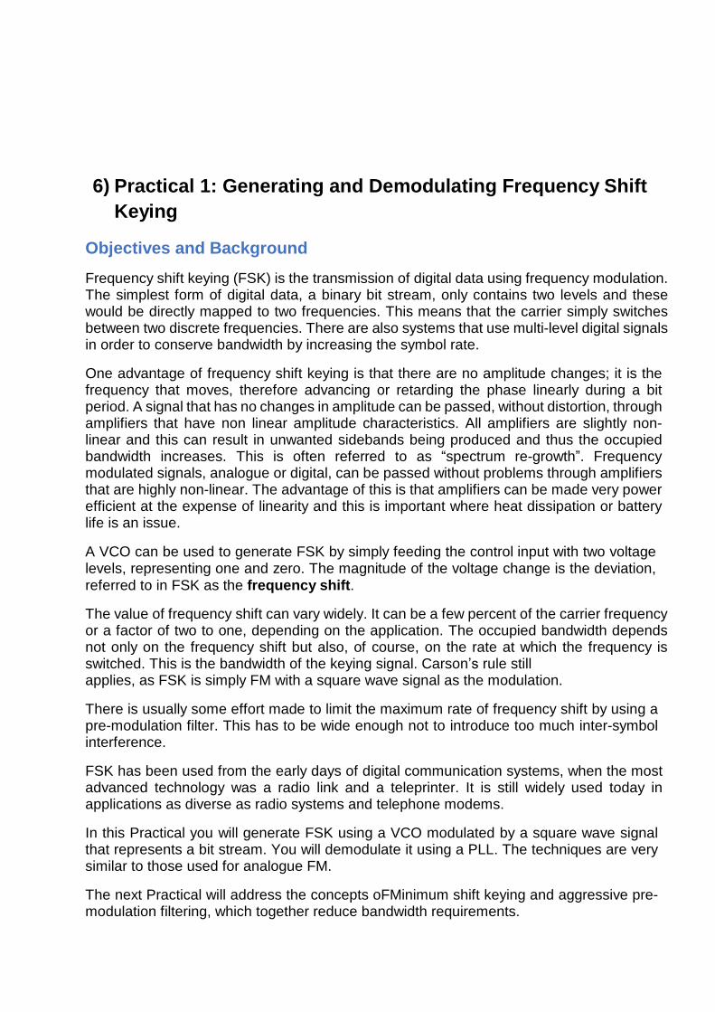
In this Practical you will generate FSK using a VCO modulated by a square wave signal that represents a bit stream. You will demodulate it using a PLL. The techniques are very similar to those used for analogue FM.
The next Practical will address the concepts oFMinimum shift keying and aggressive pre- modulation filtering, which together reduce bandwidth requirements.
Block Diagram
Make Connections Diagram
7) Practical 1: Generating and Demodulating Frequency Shift
Keying
Perform Practical
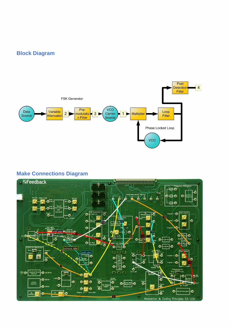
Use the Make Connections diagram to show the required connections on the hardware.
Initially you have connected up the circuit such that the Pre-modulation filter is not in circuit.
Open the oscilloscope and the frequency counter.
Set the Function Generator to Fast and select a square wave. Set the Signal Level Control to full scale to give maximum modulation. Set the IQ Demodulator controls to half scale.
Set the Frequency of the Function Generator to about 7kHz. This is the frequency of the modulation.
Note the data signal (square wave) on the lower oscilloscope trace and the upper trace (the carrier) showing no amplitude variation.
Increase the oscilloscope time-base to maximum speed and use the x expand to see the individual cycles of the carrier. Change the trigger to Channel 1 by deselecting Y2 Trig. You should be able to see the carrier changing between two frequencies.
Use the Defaults button to return the oscilloscope to the original settings.
Open the spectrum analyser and note that the two possible frequencies for the carrier are clearly visible. Adjust the modulation amplitude using the Signal Level Control and note how the frequency shift changes.
Use the Function Generator Frequency control to increase the frequency of the data (modulating) signal to about 40kHz. Note that the spectrum now shows a number of sidebands and the bandwidth is greater than the frequency shift.
Refer to the Make Connections diagram and remove connection 3 and add connections 2 and 4. This has now connected the Pre-modulation filter into the circuit.
Move the oscilloscope Channel 2 probe (yellow) to the output of the Pre-modulation filter (monitor point 3). Note, using the spectrum analyser, that the bandwidth of the signal has been reduced and, on Channel 1 of the oscilloscope, that the output of the pre-modulation filter shows the edges of the data signal are less sharp.
Adjust the Frequency of the data signal and note the effect as the frequency nears the cut-off of the filter.
Ensure that the Loop Filter Compensation switch is set to Fast.
Set the Frequency of the modulating data signal to 3kHz.
Open the voltmeter and the use it to set the amplitude to 0.15 volts ac peak to peak. Move the oscilloscope Channel 1 probe (blue) to the output of the post detection filter (monitor point 4).
Set the oscilloscope time-base to 50µS per division. You should be able to see the phase lock loop demodulating the signal. You may need to adjust the dc offset into the loop filter for the loop to lock (use the dc Source control).
Use the Signal Level Control to increase the amplitude of the modulation and thus increase the frequency shift above the PLL loop filter bandwidth. You will see that the loop cannot maintain lock.
Use the Function Generator Frequency control to increase the data (modulation) frequency. Note that as the frequency is increased the demodulated output becomes more sinusoidal as the frequency nears the loop filter cut-off.
8) Practical 2: Minimum Shift Keying
Objectives and Background
The control of signal bandwidth is an important consideration in a communications system.
Of course, there are other considerations, such as noise immunity, or how easy the system is to implement. This last consideration might be very important in a system such as a mobile phone where the size and power consumption of a handset is critical. Frequency shift keying (FSK) has the advantage of there being no amplitude variation and so is able to pass through high efficiency, non-linear amplifiers without distortion.
In Practical 1 you investigated frequency shift keying and it may have seemed that the choice of frequency shift is somewhat arbitrary. However, you saw that the smaller the shift the narrower the signal bandwidth (remembering that it cannot be less than the bandwidth of the data signal). However, a very small shift could be almost impossible to detect. What might be the optimum value to keep the bandwidth low but still make demodulation easy?
Such a system is called minimum shift keying (MSK) and can be shown to be when the shift is made half the symbol rate. MSK has another important feature, the understanding of which depends on the relationship between frequency and phase. In MSK, the phase advances when the upper frequency is sent such that it reaches +90 degrees at the end of the symbol. When the lower frequency is sent the phase retards and is –90 degrees at the end of the symbol. This means that phase detection techniques can be used both to modulate and demodulate MSK. This is quite attractive, as generating an accurate frequency deviation is very difficult but, by using the I and Q techniques, the detection of 90 degree phase shifts is easier.
All these features make MSK very suitable for mobile phone systems. A derivative of MSK called GMSK (Gaussian Minimum Shift Keying) is used in the GSM phone network.
In this Practical you will use an IQ modulator to generate an MSK signal. A simple phase demodulator is then used to demodulate the signal. The output of the demodulator represents the phase changes in signal, not the frequency changes. However, as we know that the derivative of phase is frequency, the output can simply be passed through a differentiator block to recover the original data. Unfortunately, such a block has a high pass filter characteristic and therefore has the effect of making any noise in the system more significant. In a real MSK system, the phase detector output would be used directly and processed so to minimize noise.
Note also that in this practical only a stream of ones and zeros is used. In a real system there will be situations when two ones or two zero follow each other. This means that the total phase shift will be greater than plus or minus 90 degrees. This would be dealt with by
using an IQ demodulator, rather than the simple phase demodulator used in this Practical.
Note also that, when you examine the MSK signal with the phasescope, there is a continuous frequency difference between the carrier and the modulated signal. This is not significant, since it is the phase difference at the end of each symbol that is important. However, it does make it difficult to see the 90 degree shift on the phasescope. In the Practical, this problem is resolved by using the local oscillator of the demodulator as the reference channel of the phasescope. The local oscillator is locked to the residual carrier of the modulated signal by a phase lock loop and hence follows the carrier frequency.
As you have seen, the bandwidth of the modulated signal depends on the deviation, the symbol rate and the rate of change at the symbol transitions. By adding a filter in the data signal, such that its magnitude only just reaches the symbol value at the end of the symbol, the occupied bandwidth is minimized. The filter has to have a characteristic such that, while providing filtering, the phases of all the harmonic components of the signal are preserved as much as possible. Of the various types of filter available the Gaussian filter offers the best compromise. By adding such a filter the bandwidth is minimized and the system is referred to as Gaussian Minimum Shift Keying, or GMSK.
In this Practical you will use a square wave to represent data. This is the equivalent of a series of ones and zeros. Note that, since a symbol is a one or zero and each cycle of the square wave is a one and a zero, the equivalent symbol rate is twice the square wave frequency.
Block Diagram
Make Connections Diagram
9) Practical 2: Minimum Shift Keying
Perform Practical
Use the Make Connections diagram to show the required connections on the hardware.
Set the Integrator switch to Fast, the Function Generator switch to Fast and the Loop Filter Compensation switch to Slow. Set the IQ Modulator and IQ Demodulator controls to half scale.
Open the phasescope and use the Variable Phase Shift control associated with the
Carrier Source block to set the I and Q carrier phase difference to 90 degrees.
The first part of the Practical is to estimate the deviation sensitivity of the frequency modulator block. You will do this by using dc voltages to set the modulation input and then measuring the resulting frequencies.
Open the voltmeter and frequency counter. Use the dc Source control to set the voltage to the Integrator to +0.4 volts and measure the output frequency. Note the value and set the dc voltage to –0.4v. Measure the frequency again. Now calculate the frequency difference divided by the voltage difference. This will be the modulation sensitivity in kHz per volt.
Refer to the Make Connections diagram and remove connection 20 and add connection 2. This changes the modulation source to the Function Generator output.
Open the oscilloscope. Select a square wave from the Function Generator. Move the oscilloscope Channel 2 probe (yellow) to monitor point 2.
Move the frequency counter probe (orange) to the Signal Level Control output (monitor point 3). Set the Function Generator Frequency to about 15kHz. Set the voltmeter to ac
p-p and use the Signal Level Control to set the ac amplitude to about 0.2 volts p-p. Move
the phasescope main channel probe (blue) to the MSK Generator output (monitor point 5) and set the phasescope to Constellation.
Note that you can see the phase shift but the reference position is moving. In reality it is moving round at a speed that the phasescope cannot track. Move the reference probe (yellow) to the local oscillator VCO output (monitor point 6). You should now have a ‘stable’ display, with the phase varying over an arc of phases (probably 20 degrees total
variation, centred on somewhere less than –90 degrees). If you do not, adjust the dc
Source control to lock the VCO and thus give a stable display.
Use the Signal Level Control to increase the modulation amplitude until the arc over which the phase shift varies is 90 degrees. This is not easy to estimate but do your best. Now measure the modulation ac p-p amplitude on the voltmeter. By using the value you have calculated for the frequency sensitivity of the modulator, you can now calculate the frequency deviation required for this 90 degrees shift per symbol. Remember here that the
symbol rate is represented by twice the function generator frequency. This should confirm that the deviation is half the symbol rate for MSK.
On the oscilloscope you should be able to see the phase changing over the 90 degree range. Move the oscilloscope channel 1 probe (blue) to the output of the integrator (monitor point 4). The signal should be an integrated square wave (i.e. a triangle). You will have to adjust the oscilloscope timebase to see this clearly. Compare this to the phase detector output at the post detection filter (monitor point 7).
The differentiated output at monitor point 8 should be similar the original data (on monitor point 3), although the differentiated output will probably be somewhat rounded.
Move the Y2 probe (blue) back to the phase detector output (monitor point 7) and increase the Signal Level Control to increase the deviation, so the phase shift is greater than 90 degrees. Observe the fact that the output is no longer a triangle wave but has become distorted.
10) Practical 3: Multi-level Frequency Shift Keying
Objectives and Background
In Practical 1 binary FSK was generated, where two frequencies were transmitted. It is possible to have a system where the data causes the carrier to switch between one of, say, 4 or 8 frequencies. Such as system is called multi frequency shift keying or MFSK. Many different systems exist, using anything from 4 to 50 frequencies. They can be very efficient but, as the number of frequencies increases, so does the difficulty in demodulating them.
Using more than two frequencies will increase the bit rate for a constant symbol rate. MFSK
can also be used to increase the noise immunity of a system by keeping the bit rate the same but increasing the number of frequencies and hence reducing the symbol rate.
Note also that the bandwidth depends on the symbol rate BUT cannot be less than the total range of the FSK frequencies. This means that, in a system that uses MFSK to increase noise immunity, the bandwidth is often increased as a consequence.
Demodulation of higher order MFSK is usually performed by using DSP, because implementing all the required analogue filtering would need so much electronic hardware.
In this Practical you will see 4, 8 and 16 frequencies being used.
Block Diagram
Make Connections Diagram
11) Practical 3: Multi-level Frequency Shift Keying
Perform Practical
Use the Make Connections diagram to show the required connections on the hardware.
Set the Signal Level Control to half scale.
Open the oscilloscope and note the lower trace (yellow) showing the signal being applied to the VCO. Use the buttons on the block diagram to change to 8 level and 4 level data and check that the number of levels corresponds with the changes in data format. You may need to increase the size of the oscilloscope to verify this.
Increase the timebase speed on the oscilloscope and change the trigger to
Channel 1 (deselect Y2 Trig). Note the carrier frequency (blue trace) changing.
Set the Compensation switch associated with the Loop Filter to Fast.
Move the Channel 1 probe (blue) to the post detection filter demodulated output (monitor point 4). The PLL may not be locked so you may not see demodulated recognisable data. Turn the modulation deviation down (using the Signal Level Control) and use the dc Source control to lock the loop.
You should be able to see the multilevel data on the demodulated output. Again you should appreciate that although more data is carried per symbol it is more likely that the wrong symbol will be recovered.
Move the oscilloscope Channel 1 probe back to the VCO output (monitor point 1). Use the button on the block diagram to select 4 level data.
Open the spectrum analyser. Use the default button on the oscilloscope to return the settings to the original ones.
Use the Signal Level Control to turn the modulation deviation to maximum. You should be able to see a typical FSK spectrum on the analyser.
Change the data to 8 level and 16 level. The spectrum becomes less like a binary FSK signal.
In order to see the individual frequencies, use the buttons on the block diagram to reduce the symbol rate to 5 symbols per second. You can now see the individual frequencies on the spectrum analyser.
Increase the oscilloscope timebase speed and use the expand control so you can see individual carrier cycles. Trigger off Channel 1 (deselect Y2 Trig) and now see
how the frequency is changing. Change the number of levels in the data and compare the number of individual frequencies shown on the spectrum analyser to the number of levels in the data.