Page 1
ELECTRICAL AND STRUCTURAL PROPERTIES OF ZnSe THIN FILMS BY ELECTRODEPOSITION TECHNIQUE
I. L. IKHIOYA1 and A. J. Ekpunobi2
Department of physics and Industrial Physics, Nnamdi Azikiwe University, Awka, Anambra State, Nigeria. 1Email: [email protected] , Mobile no: +23408038684908 2Email: [email protected] , Mobile no: +23408038763056
ABSTRACT
Zinc selenide (ZnSe) thin films semiconductor were studied at room temperature by
electrodeposition technique. XRD pattern of ZnSe showed cubic structure with a preferred
orientation along (111) plane. The optical properties of the films were investigated in the
wavelength range of 300-900nm. The optical band gap energy was 2.3-2.1eV.
Keywords: Thin Film, ITO, ZnSe, Seo2, characterization, application.
1. INTRODUCTION
Zinc selenide is an n-type semiconducting material with wide band gap (2.7 eV). It is a
suitable material for red, blue and green light emitting diodes, photovoltaic, laser screens,
thin film transistors, photoelectrochemical cells[1- 4]. The buffer layer determines
properties of thin film solar cells such as intensity of the electric field in the absorber
interfacial states and electronic bands alignment. It is also involved in the long-term stability
of the cells and light soaking effect [5]. ZnSe thin film has been used as n-type window layer
for thin film herterojunction solar cells [6]. Thin films of ZnSe have been deposited using
molecular beam epitaxy, electron beam evaporation, chemical deposition,
electrodeposition, vacuum evaporation, successive ionic layer adsorption and reaction
(SILAR) technique [7 – 11]. Electrodeposition technique seems to be an inexpensive, low
temperature method that could produce good quality films for device applications. The
attractive features of this method are the convenience for producing large area devices and
Page 2
possibility to control the film thickness, morphology and stoichiometry of the films by
adjusting the deposition parameters and concentration of precursors in electrolyte.
In this paper, we report the electrodeposition of ZnSe thin films from an aqueous solution
bath containing ZnSo4.7H2O and SeO2. The influence of growth conditions such as
deposition potential, temperature on crystallininty and composition of the film was studied.
XRD and optical transmission techniques were employed for characterizing the deposited
films.
2. MATERIALS AND METHODS
ZnSe thin films were deposited by electrodeposition technique using 20cm3 of 0.063m of
selenium IV oxide (Seo2) mixed 20cm3 of 0.069m of Zinc tetraoxosulphate VI Heptehydrate
(ZnSo4.7H2O) and 5cm3 of potassium tetraoxosulphate VI (K2SO4) solution then, 5cm3 of
0.4m of tetraoxosulphate VI acid (H2SO4). Which used to acidify the solution, it was added
into the mixture and stirred well. The indium doped tin oxide (ITO) glass was used as
substrate. The ultrasonically cleaned glass substrate was immersed vertically into the
solution for electrodeposition process. The films growth was carried out at 300k. During
deposition process, the deposited films were tested for adhesion by subjecting it to a steady
stream of distilled water. X- Ray diffractometer (XRD) analysis was carried out using DM-10
diffractometer for the 2θ ranging from (15- 530) with CuKal (λ = 1.540598Ǻ) radiation.
Optical absorbance study was carried out using M501 UV-Visible spectrophotometer. The
films coated indium thin oxide glass was placed across the sample radiation pathway while
the uncoated the reference path. The absorption data were manipulated for the
determination of band gap energy
Page 3
3. ELECTRICAL ANALYSIS OF ZnSe FILMS
The electrical properties of the films were investigated using a standard four point probe
technique. The arrangement was made in such a way that the voltage across the transverse
distance of the films and the corresponding values of the current were measured using
silver paste to ensure good ohmic contact to the film. Table 1 shows the result obtained.
The results clearly show that ZnSe films have high resistivity. The high resistivity makes ZnSe
suitable as buffer layer in thin film technology. It is a semiconductor that has large potential
applications in thin films like photo luminescence and electroluminescent devices. The
results are comparable with the value reported in [12], whose value of resistivity is of the
order of 10 4- 1012(Ω𝑚)−1 [13-14]
TABLE 1. Electrical property of ZnSe films
SLIDES THICKNESS, t
(𝒏𝒎)
RESISTIVITY, ℓ
(Ω𝒎)−𝟏
CONDUCTIVITY, σ
(Ω𝒎)−𝟏
X 164 1.500x10⁸ 7.892x10⁻⁵
Y 201 4.861x10⁹ 2.057x10⁻⁶
Z 220 4.339x10⁹ 2.304x10⁻⁴
Page 4
4. STRUCTURAL PROPERTIES OF ZINC SELENIDE FILMS X-ray diffractometer using CuKal radiation (λ = 1.540598 Ǻ). The X-ray diffraction patterns of
ZnSe thin films are presented in Figure.1-3. The X-ray diffraction patterns show a cubic
structure which correspond to (111-222) planes. The diffraction angle 2ϴ value is 16.310,
16.610 and 16.170 with d = 5.432Å, d = 5.336Å and d = 5.480Ǻ. The preferred orientation lies
along the (111) plane. The lattice constant was given in the X-ray diffraction analysis is
found to be a = 5.6667Ǻ. The crystallite size was determined by means of the X-ray line
broadening method using Scherer equation [15]
D = 0.94𝜆
𝛽𝐶𝑜𝑠𝜃 (1)
Where λ is the wavelength of CuKal radiation (λ = 1.540598 Ǻ), is the full width of half 𝜷
maximum FWHM of the (hkl) peak of the diffracting angle hkl 2θ. The average grain size D,
the dislocation density δ is calculated using the following relation [16]
δ = 1
𝐷2 lines/m2 (2)
Page 5
Figure 1: X-ray diffraction pattern of ZnSe film (slide X)
Table 2. The structural parameters of ZnSe film (X)
Slid
e
H k
l
2θ
d(Ǻ
) me
asu
red
d(Ǻ
) sta
nd
ard
Latt
ice
con
stan
t
(Ǻ)
FWH
M (
rad
.)
Gra
in s
ize,
(D
)(Ǻ
)
𝒙 𝟏
𝟎−
𝟏𝟎
Dis
loca
tio
n
den
sity
, 𝛔
x 𝟏
𝟎−
𝟐𝟎
Mic
ro s
trai
n ε
Deg
.
Rad
.
X 111 16.31 0.284 5.431 5.432 5.67 0.76246 1.836 1.330 0.565
200 16.99 0.296 5.218 5.219 0.76246 1.837 1.276 0.613
220 17.31 0.302 5.122 5.123 0.76246 1.838 1.252 0.637
311 17.78 0.310 4.987 4.988 0.76246 1.839 1.218 0.673
222 18.10 0.315 4.900 4.901 0.76246 1.840 1.196 0.698
Page 6
Figure 2: X-ray diffraction pattern of ZnSe film (slide Y)
Table 3. Structural parameters of ZnSe film (Y)
Slid
e
H k
l
2θ
d(Ǻ
) me
asu
red
d(Ǻ
) sta
nd
ard
Latt
ice
con
stan
t
(Ǻ)
FWH
M (
rad
.)
Gra
in s
ize,
(D
)(Ǻ
)
𝒙 𝟏
𝟎−
𝟏𝟎
Dis
loca
tio
n
den
sity
, 𝛔
x 𝟏
𝟎−
𝟐𝟎
Mic
ro s
trai
n ε
Deg
.
Rad
.
Y 111 16.61 0.289 5.335 5.336 5.67 0.61122 2.291 1.046 0.912
200 20.43 0.356 4.345 4.346 0.14643 9.617 2.617 0.242
220 20.65 0.360 4.299 4.300 0.16597 8.488 0.227 1.927
311 20.98 0.366 4.233 4.234 0.65342 0.882 0.882 1.284
222 21.37 0.372 4.157 4.158 0.4173 0.552 0.552 3.270
Page 7
Figure 3: X-ray diffraction pattern of ZnSe film (slide Z)
Table 4. Structural parameters of ZnSe film (Z)
Slid
e
H k
l
2θ
d(Ǻ
) me
asu
red
d(Ǻ
) sta
nd
ard
Latt
ice
con
stan
t
(Ǻ)
FWH
M (
rad
.)
Gra
in s
ize,
(D
)(Ǻ
)
𝒙 𝟏
𝟎−
𝟏𝟎
Dis
loca
tio
n
den
sity
, 𝛔
x 𝟏
𝟎−
𝟐𝟎
Mic
ro s
trai
n ε
D
eg.
Rad
.
Z 111 16.17 0.282 5.479 5.480 5.67 1.1452 1.222 2.015 0.246
200 17.72 0.309 5.004 5.005 0.45208 3.102 0.725 1.902
220 20.60 0.359 4.309 4.310 0.6999 2.012 0.962 1.078
311 21.25 0.370 4.179 4.180 0.49187 1.410 0.655 2.327
222 21.61 0.377 4.111 4.112 0.37872 3.725 0.496 4.063
Page 8
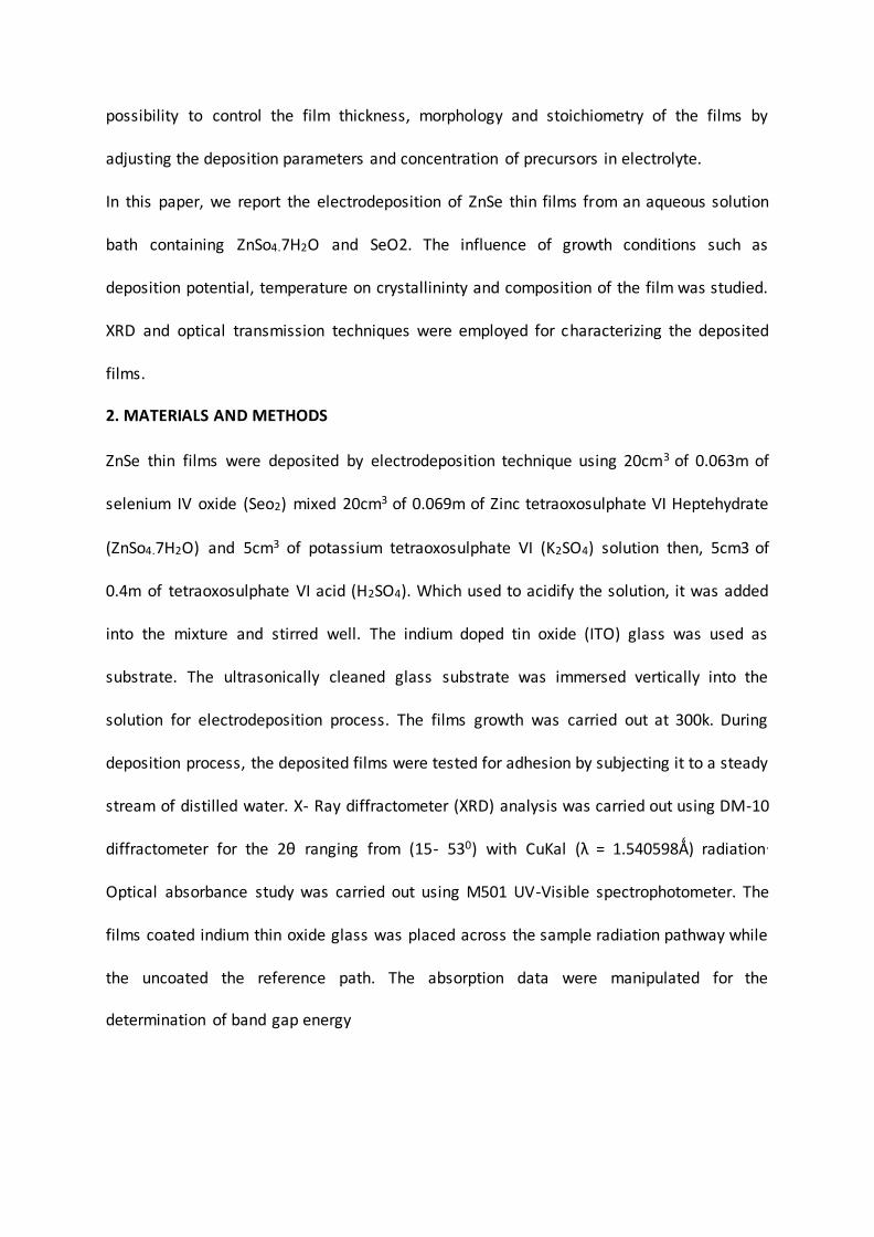
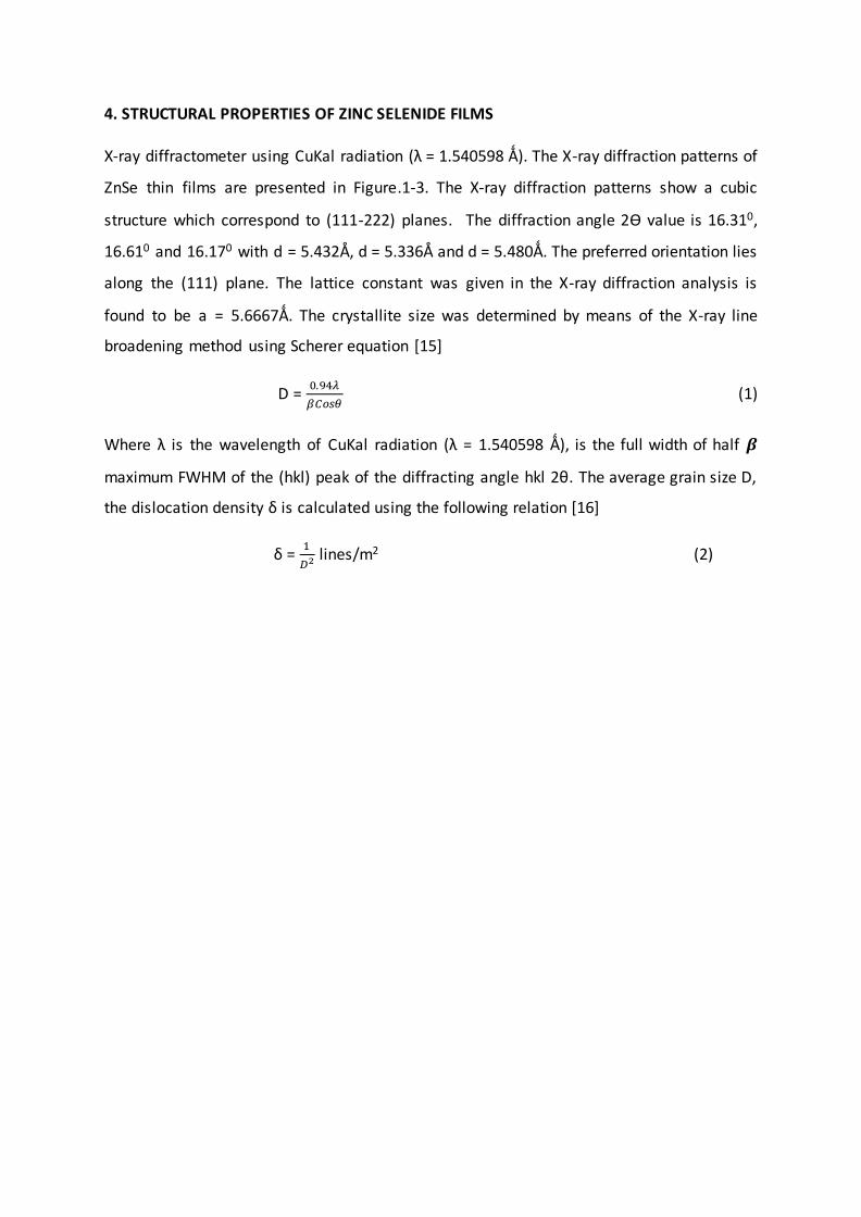
5. OPTICAL PROPERTIES OF ZINC SELENIDE FILMS
The optical properties of Zinc selenide films were studied using a M501 UV-Visible
spectrophotometer in a wavelength range of 300-900nm.The transmission spectra of the
Zinc selenide thin films deposited shows in Figure 5. The transmittance spectra show very
high transmittance in the VIS-NIR regions of the electromagnetic spectrum. In Figure 4 the
absorbance of Zinc selenide film show high in the UV region and IR regions. The high
absorbance in UV region makes the material useful in formation of p-n junction solar cells
with other suitable thin film materials for photovoltaic application. These results agree well
with the report in [12]. These optical properties make Zinc selenide thin films nice glazing
material for maintaining cool interior in buildings in warm climate regions while still keeping
the rooms well illuminated. To ensure that the thermal radiation from the warm glazing to
the interior is inhibited and the thermal energy dissipated in the glazing due to absorption is
predominantly transferred to the exterior by enhanced convective heat transfer of the
glazing to the exterior.
Figure 4: Plot of absorbance against photon energy for ZnSe Film (slide XYZ
0
0.02
0.04
0.06
0.08
0.1
0.12
0.14
0.16
0 1 2 3 4 5
Ab
sorb
ance
(arb
itra
ry u
nit)
Photon Energy, eV
SLIDE X
SLIDE Y
SLIDE Z
Page 9
Figure 5: Plot of transmittance against wavelength for ZnSe film (slide XYZ)
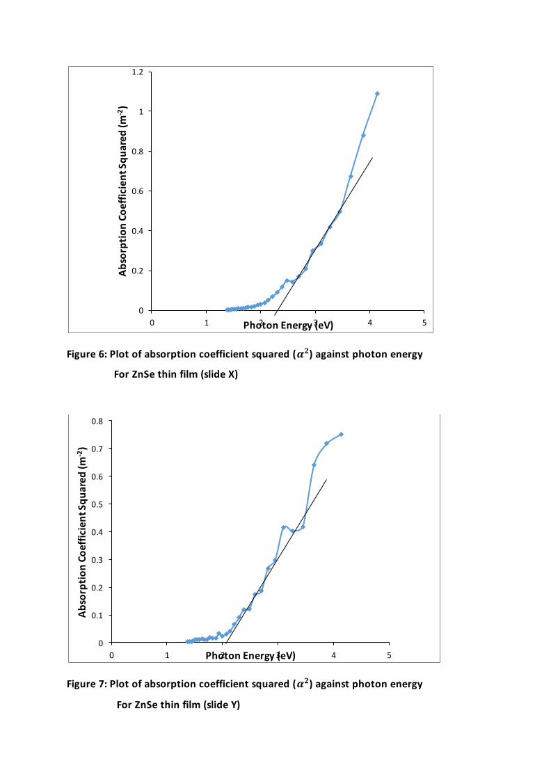
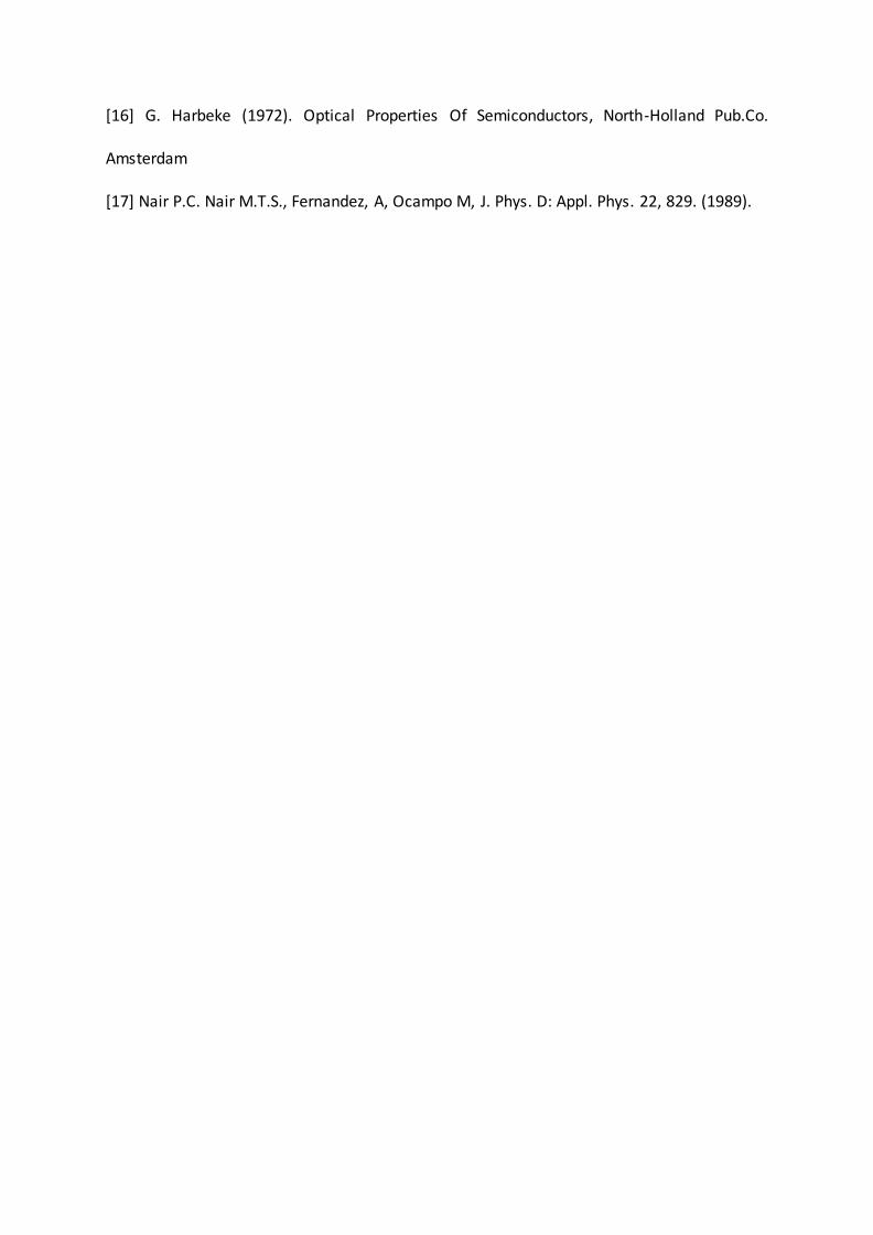
The Band Gap Energy
The band gap energy and transition types were derived from mathematical processing of
the data obtained from the optical absorbance versus photon energy with the following
relationships for near edge absorption [17].
α = (hυ –εg) n/2
Where υ is the frequency, h is the Planck’s constant, while n carries the value of either 1 or
4. The band gap εg could be obtained from a straight line plot of α² as a function of hυ; an
extrapolation of the value of α² to zero will give band gap. If a straight line graph is obtained
from n=1, it indicates a direct transition between the states of the semiconductor, whereas
the transition is indirect if a straight line graph is obtained from n = 4 as shown in Figure 6.
The band gap energy of 2.3eV band gap energy has been obtained which correspond to the
band gap energy obtain in [14]. Band gap energy of 2.1eV and 2.2eV was obtained in Figures
7-8 due to slight increase in pH
0
0.1
0.2
0.3
0.4
0.5
0.6
0.7
0.8
0.9
1
0 200 400 600 800 1000
Tran
smit
tan
ce (%
)
Wavelength (nm)
SLIDE X
SLIDE Y
SLIDE Z
Page 10
Figure 6: Plot of absorption coefficient squared (𝜶𝟐) against photon energy
For ZnSe thin film (slide X)
Figure 7: Plot of absorption coefficient squared (𝜶𝟐) against photon energy
For ZnSe thin film (slide Y)
0
0.2
0.4
0.6
0.8
1
1.2
0 1 2 3 4 5
Ab
sorp
tio
n C
oe
ffic
ien
t Sq
ua
red
(m-2
)
Photon Energy (eV)
0
0.1
0.2
0.3
0.4
0.5
0.6
0.7
0.8
0 1 2 3 4 5
Ab
sorp
tio
n C
oef
fici
ent S
qu
ared
(m-2
)
Photon Energy (eV)
Page 11
Figure 8: Plot of absorption coefficient squared (𝜶𝟐) against photon energy
For ZnSe thin film (slide Z)
6. Conclusion
Zinc selenide thin films have been prepared by electrodeposition technique. The films have
peak transmittance in infrared region of the electromagnetic spectrum and high rate of
absorption in the UV and NIR regions. These make Zinc selenide thin films excellent glazing
material for solar control in warm climatic regions. The obtained value of the optical band
gap energy was 2.7eV, and the relation indicates indirect transition. XRD analysis showed
that the ZnSe thin films, so deposited, exhibit cubic structure with a preferred orientation
along (111) plane.
References
[1] O. Akira, S. Noriyoshi, S. Zembutsu, J. Appl. Phys. 64, 654 (1988).
0
0.05
0.1
0.15
0.2
0.25
0.3
0.35
0.4
0.45
0 1 2 3 4 5
Ab
sorp
tio
n C
oef
fici
ent S
qu
ared
(m-2
)
Photon Energy (eV)
Page 12
[2] A. Ennaoui, S. Siebntritt, M.Ch. Lux-Steiner, W. Riedl, F. Karg, Solar Energy Mater. Solar
Cells 67, 31 (2001).
[3] M. P. Kulapov, G. A. Murovick, V. N. Ulasyuk et al., lzv Akad Nauk SSSR Neorg. Mater. 19,
1807 (1983).
[4] R. R. Alfano, O. Z. Wang, J. Jumbo, B. Bhargava, J. Phys. Rev. A 35, 459 (1987).
[5] A. M. Chaparro, M. T. Gutierrez, J. Herrero, J. Klaer, Mater. Res. Soc. Symp.Proc. 668,
(2001).
[6] N. Katsumura, K. Maemura, T. Mori, J. Saraie, J. Crystal Growth,159,85(1996).
[7] R. Islam, D.R. Rao, J. Mater. Sci. Lett., 13, 1637 (1994).
[8] A. M. Chaparro, M. T. Gutierez, J. Herero, Electrochim. Acta, 47,977(2001).
[9] A. Chandramohan, T. Mahalingam, J.P. Chu, P.J. Sebastian, Sol.Energy Mater. Sol.
Cells, 81,371 (2004).
[10] P. K. R. Kalita, B. K. Sarma, H. L. Das, Bull. Mater. Sci, 23,313 (2000).
[11] R. B. Kale, C.D. Lokhande, Mater. Res. Bull, 39, 1829 (2004).
[12] Zulfiqar Ali, Akram K.S. Aqili, M. Shafique, Asghari Maqsood (2006). Physical properties
of ZnSe films prepared by two-source evaporation and a study of post doping effect, Journal
of Non-crystalline solids 352. Pp.409-414.
[13] K.R. Murali, K. Thilakvathy, S. Vasantha, Rachel Ooomen. (2008). Properties of ZnSe
Films Pulse Plated on High Temperature Substrates, Chalcogenide Letter Vol. 5, No.6,
pp.111-116.
[14] N.A.Okereke, A.J. Ekpunobi (2011). ZnSe buffer layer deposition for solar cell
application. Journal of Non-Oxide Glasses, vol. 3 No.1, No. 3, pp.31-36
[15] Abeles, F. (Ed). Optical Properties Of Solid, North-Holland Pub.Co. Amsterdam.
Page 13
[16] G. Harbeke (1972). Optical Properties Of Semiconductors, North-Holland Pub.Co.
Amsterdam
[17] Nair P.C. Nair M.T.S., Fernandez, A, Ocampo M, J. Phys. D: Appl. Phys. 22, 829. (1989).