Electrical Conduction Mechanism in Chemically Derived Graphene Monolayers Alan B. Kaiser, † Cristina Gómez-Navarro, ‡, * Ravi S. Sundaram, ‡ Marko Burghard, ‡ and Klaus Kern ‡,§ MacDiarmid Institute for AdVanced Materials and Nanotechnology, SCPS, Victoria UniVersity of Wellington, PO Box 600, Wellington, New Zealand, Max-Planck-Institutfuer Festkoerperforschung , Heisenbergstrasse 1, 70569 Stuttgart, Germany, and Ecole Polytechnique Federale de Lausanne, CH-1015 Lausanne, SwitzerlandReceived Decembe r 8, 2008; Revised Manuscri pt Received February 23, 2009ABSTRACT We have performed a detailed study of the intrinsic electrical conduction process in individual monolayers of chemically reduced graphene oxide down to a temperature of 2 K. The observed conductance can be consistently interpreted in the framework of two-dimensional variable- range hopping in parallel with electric-field-driven tunneling. The latter mechanism is found to dominate the electrical transport at very low temperatures and high electric fields. Our results are consistent with a model of highly conducting graphene regions interspersed with disordered regions, across which charge carrier hopping and tunneling are promoted by strong local electric fields. Graphene, consisting of a layer of carbon atoms just one atom thick, is the ultimate in thin conducting sheets. 1 The charg e carrie rs can be tuned from electron- like to hole- like by the application of a gate voltage, 2 and very high carrier mobilities have been reported. 3 Future electronics applica- tions envisage the creation of diverse nanoscale elements ofelectronic circuits on a single graphene sheet. 1,4 However, pr og ress in this di re ct ion is hamp er ed by the li mi ted availability of high-quality, large size graphene sheets. A pro mis ing sol uti on to thi s pro ble m compri ses chemical conv ersio n of readi ly accessible mono layer s of grap hene oxide (GO) to gra phe ne. 5,6 To date, che mic ally der ive d gra phene obtained in thi s man ner exhibits an electr ica l conductivity of the order of a few Siemens per centimeter (approximately 3 orders of magnitude below that of pristine graphene layers 2,7 ), which is useful for various applications such as transparent conducting electrodes 8 in photovoltaic cells 9-11 or electrically conductive composite materials. 12,13 The GO route is furthermore attractive since it may enable implementing electrically active graphene regions together with well-defined charge transport barriers made of GO into the same sheet. 14,15 However, at the present stage only little is kno wn abo ut the inh erent mic ros cop ic str uct ure and mec han ism of ele ctr ical con duc tion, des pit e the ir gre at importance for the further improvement of this material. It is well- docu mente d that GO-d erive d grap hene contains a signi ficant amount of resid ual defec ts, 6,16 and a det aile d knowledg e of how char ge tr ansport oc curs in such a structurally and electronically inhomogeneous system could aid identifying synthetic strategies to more closely approach the electrical performance of pristine graphene. Scann ing tunn eling microsco py (STM) of reduced GO monolaye rs ha s reve al ed that the he xago na l latti ce of graphen e sheets is partially preserve d, but disord ered regions ascribed to the presence of oxygenated functional groups are also present. 6 Moreover, the evaluation of Raman spectro- scopic data on the basis of the empirical Tuinstra-Koenig expression 17 relating the intensity ratio of the Raman D and G modes to the crystallite size of graphitic samples provided an estimated size of the intact graphene regions on the order of 6 nm. Regarding the charge transport mechanism in GO- derived graphen e, no conclusiv e picture has evolved so far. 18 In fact, while a previous study suggests the relevance ofhopping conduction, 6 electrical measurements on overlapping platelets of reduced GO could be best interpreted in terms of tunneling through Schottky barriers at the gold contacts. 19 Similar to the latter case, the electrical resistance of GO flakes deposited between two epitaxial graphene electrodes has been found to be pr imar ily due to Schottk y ba rriers at the contacts. 20 As the cur ren t-vol tag e behavior showed no systemat ic de pe ndence on the gap wi dt h be tween the electrodes, it was concluded that the dominant contribution * Corresponding author, [email protected]. † Victoria University of Wellington. ‡ Max-Planck-Institut fuer Festkoerperforschung. § Ecole Polytechnique Federale de Lausanne. NANO LETTERS 2009 Vol. 9, No. 5 1787-1792 10.1021/nl803698b CCC: $40.75 2009 American Chemical Society Published on Web 03/30/2009
Transcript
7/27/2019 Electrical Conduction Mechanism in Chemically Derived Graphene Monolayers
Alan B. Kaiser,† Cristina Gómez-Navarro,‡,* Ravi S. Sundaram,‡ Marko Burghard,‡
and Klaus Kern‡,§
MacDiarmid Institute for Ad Vanced Materials and Nanotechnology, SCPS, Victoria
UniVersity of Wellington, PO Box 600, Wellington, New Zealand, Max-Planck-Institut
fuer Festkoerperforschung, Heisenbergstrasse 1, 70569 Stuttgart, Germany, and Ecole
Polytechnique Federale de Lausanne, CH-1015 Lausanne, Switzerland
Received December 8, 2008; Revised Manuscript Received February 23, 2009
ABSTRACT
We have performed a detailed study of the intrinsic electrical conduction process in individual monolayers of chemically reduced graphene
oxide down to a temperature of 2 K. The observed conductance can be consistently interpreted in the framework of two-dimensional variable-
range hopping in parallel with electric-field-driven tunneling. The latter mechanism is found to dominate the electrical transport at very low
temperatures and high electric fields. Our results are consistent with a model of highly conducting graphene regions interspersed with disordered
regions, across which charge carrier hopping and tunneling are promoted by strong local electric fields.
Graphene, consisting of a layer of carbon atoms just one
atom thick, is the ultimate in thin conducting sheets. 1 The
charge carriers can be tuned from electron-like to hole-like
by the application of a gate voltage,2 and very high carrier
mobilities have been reported.3
Future electronics applica-tions envisage the creation of diverse nanoscale elements of
electronic circuits on a single graphene sheet.1,4 However,
progress in this direction is hampered by the limited
availability of high-quality, large size graphene sheets. A
promising solution to this problem comprises chemical
conversion of readily accessible monolayers of graphene
oxide (GO) to graphene.5,6 To date, chemically derived
graphene obtained in this manner exhibits an electrical
conductivity of the order of a few Siemens per centimeter
(approximately 3 orders of magnitude below that of pristine
graphene layers2,7), which is useful for various applications
such as transparent conducting electrodes8 in photovoltaic
cells9-11 or electrically conductive composite materials.12,13
The GO route is furthermore attractive since it may enable
implementing electrically active graphene regions together
with well-defined charge transport barriers made of GO into
the same sheet.14,15 However, at the present stage only little
is known about the inherent microscopic structure and
mechanism of electrical conduction, despite their great
importance for the further improvement of this material. It
is well-documented that GO-derived graphene contains a
significant amount of residual defects,6,16 and a detailed
knowledge of how charge transport occurs in such a
structurally and electronically inhomogeneous system could
aid identifying synthetic strategies to more closely approachthe electrical performance of pristine graphene.
Scanning tunneling microscopy (STM) of reduced GO
monolayers has revealed that the hexagonal lattice of
graphene sheets is partially preserved, but disordered regions
ascribed to the presence of oxygenated functional groups are
also present.6 Moreover, the evaluation of Raman spectro-
scopic data on the basis of the empirical Tuinstra-Koenig
expression17 relating the intensity ratio of the Raman D and
G modes to the crystallite size of graphitic samples provided
an estimated size of the intact graphene regions on the order
of 6 nm. Regarding the charge transport mechanism in GO-derived graphene, no conclusive picture has evolved so far.18
In fact, while a previous study suggests the relevance of
hopping conduction,6 electrical measurements on overlapping
platelets of reduced GO could be best interpreted in terms
of tunneling through Schottky barriers at the gold contacts.19
Similar to the latter case, the electrical resistance of GO flakes
deposited between two epitaxial graphene electrodes has been
found to be primarily due to Schottky barriers at the
contacts.20 As the current-voltage behavior showed no
systematic dependence on the gap width between the
electrodes, it was concluded that the dominant contribution
* Corresponding author, [email protected].† Victoria University of Wellington.‡ Max-Planck-Institut fuer Festkoerperforschung.§ Ecole Polytechnique Federale de Lausanne.
NANO
LETTERS
2009Vol. 9, No. 5
1787-1792
10.1021/nl803698b CCC: $40.75 2009 American Chemical SocietyPublished on Web 03/30/2009
7/27/2019 Electrical Conduction Mechanism in Chemically Derived Graphene Monolayers
to the measured resistance came from the contacts, and not
the bulk resistance of the GO flake.
In this Letter, we report a detailed investigation of the
intrinsic mechanisms of conduction in reduced GO mono-
layers. For our configuration and samples, the intrinsic
resistance of the reduced GO sheets dominates over the
graphene-
electrode contact resistances. We measure andanalyze currents as a function of electric field, gate voltage,
and temperature down to 2 K. Our results on the conduction
process in reduced GO sheets are relevant for the develop-
ment of nanoscale devices comprised of patterned graphene
sheets14,15 and furthermore enable us to draw intriguing
parallels to organic conducting polymers and carbon nano-
tubes, which display related structural features but a different
dimensionality of their underlying π -systems.21
Graphite oxide prepared by the Hummers method22 starting
from graphite flakes was dispersed in water and deposited
on a Si substrate with a 300 nm thick thermally grown SiO2
layer that was previously surface-modified by amino-
silanization. The resulting GO layers were chemically
reduced by hydrogen plasma treatment, following an opti-
mized procedure to obtain maximum electrical conductivity.6
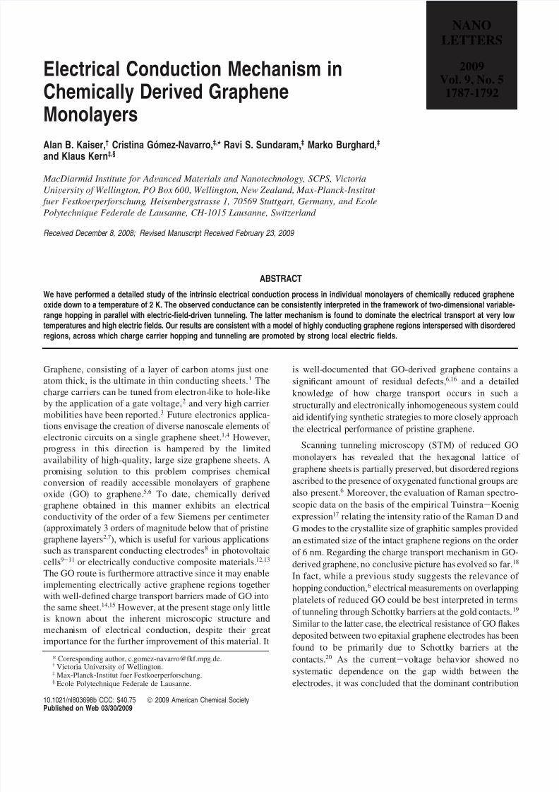
Individual GO monolayers, with atomic force microscope
(AFM) heights of ∼1 nm, were provided with Ti/AuPd (0.3/
25 nm) top contacts by e-beam lithography (Figure 1). For
temperature-dependent electrical transport measurements, the
samples were placed inside an Oxford Instrument cryostat
under a low pressure of helium.
The investigation of GO monolayers contacted by a set
of electrodes with varying distance revealed that their
electrical resistance increases linearly with electrode separa-
tion (Figure 2a). This dependence shows that the total
resistance of our samples is mainly governed by the intrinsic
sheet resistance, rather than the contact resistance that in
general should be independent of sample length. Further
support for this conclusion stems from the fact that the
temperature dependence of the measured source-drain
current I does not fit well (Figure 2b) to the behavior
expected for Schottky barrier-limited charge transport.20,23
The latter model has recently been successfully applied to
GO sheets subjected to mild thermal annealing instead of
chemical reduction.20 Besides a different chemical composi-
tion, the contact-dominated behavior observed in ref 20 may
originate from the use of bottom gold electrodes forcontacting the sheets, as distinguished from our noble metal
contacts evaporated on top. In analogy to previous studies
on carbon nanotubes,24 such a configuration is expected to
cause significant bending of the sheets at the electrode edges,
which is likely to introduce a local potential barrier.
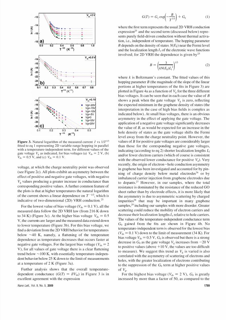
We are able to give an excellent account of our data down
to a temperature of about 40 K in terms of variable-range
hopping (VRH). In Figure 3, the current I measured between
2 and 200 K through a chemically reduced GO sheet at
different gate voltages V g from -20 to +20 V is compared
for three different values of bias voltage V ds. In each case,
the current (and so conductance) is smallest for zero gate
Figure 1. An example of a reduced graphene oxide sample on aSi/SiO2 substrate with Ti/AuPd (0.3/25 nm) top contacts.
I (T ) ∝ T 3/2
exp(-1/ T )
Figure 2. (a) Room-temperature resistance (measured at a voltageof (100 mV) increasing linearly with electrode separation, il-lustrating that it arises primarily from the intrinsic resistance of the GO sheet rather than contact resistance at the electrodes. Theinset shows the electrode configuration for the measurements. (b)Temperature dependence of the current I for a reduced GO sample(length 1.1 µm, width 1.3 µm), for a bias voltage of 0.1 V anddifferent values of the gate voltage V g (as shown), compared to thelinear behavior (dashed lines) expected in this plot for the Schottkymodel. (c) Resistance as a function of gate voltage for the samesample as in panel b at 220 K under a low pressure of helium.
1788 Nano Lett., Vol. 9, No. 5, 2009
7/27/2019 Electrical Conduction Mechanism in Chemically Derived Graphene Monolayers
voltage, at which the charge neutrality point was observed(see Figure 2c). All plots exhibit an asymmetry between the
effect of positive and negative gate voltages, with negative
V g values producing a greater increase in conductance than
corresponding positive values. A further common feature of
the plots is that at higher temperatures the natural logarithm
of the current shows a linear dependence on T -1/3, which is
indicative of two-dimensional (2D) VRH conduction.25
For the lowest value of bias voltage (V ds ) 0.1 V), all the
measured data follow the 2D VRH law (from 216 K down
to 34 K) (Figure 3c). At the higher bias voltage V ds ) 0.5
V, the currents are larger and the measured data extend down
to lower temperature (Figure 3b). For this bias voltage, wefind a deviation from the 2D VRH behavior for temperatures
below ∼40 K, namely, a flattening of the temperature
dependence as temperature decreases that occurs faster at
negative gate voltages. For the largest bias voltage (V ds ) 2
V), for all values of gate voltage there is a clear flattening
trend below ∼100 K, with essentially temperature-indepen-
dent behavior below 25 K down to the limit of measurements
at a temperature of 2 K (Figure 3a).
Further analysis shows that the overall temperature-
dependent conductance (G(T ) ) I / V ds) in Figure 3 is in
excellent agreement with the expression
where the first term represents the usual 2D VRH conduction
expression25 and the second term (discussed below) repre-
sents purely field-driven conduction without thermal activa-
tion, i.e., independent of temperature. The hopping parameter
B depends on the density of states N ( E F) near the Fermi level
and the localization length Ll of the electronic wave functions
involved; for 2D VRH the dependence is given by25
where k is Boltzmann’s constant. The fitted values of this
hopping parameter B (the magnitude of the slope of the linear
portions at higher temperatures of the fits in Figure 3) are
plotted in Figure 4a as a function of V g for the three different
bias voltages. It can be seen that in each case the value of B
shows a peak when the gate voltage V g is zero, reflecting
the expected minimum in the graphene density of states (the
interpretation in the case of high bias fields is complex as
indicated below). At small bias voltages, there is an obvious
asymmetry in the effect of applying the gate voltage. The
application of a negative gate voltage significantly decreases
the value of B, as would be expected for an increase in the
hole density of states as the gate voltage shifts the Fermi
level away from the charge neutrality point. However, the
values of B for positive gate voltages are considerably larger
than those for the corresponding negative gate voltages,
indicating (according to eq 2) shorter localization lengths Ll
and/or fewer electron carriers (which of course is consistent
with the observed lower conductance for positive V g). Very
recently, the origin of electron-hole conduction asymmetry
in graphene has been investigated and accounted for by pin-ning of charge density below metal electrodes26 or by
imbalanced carrier injection from graphene electrodes due
to dopants.27 However, in our samples, where the total
resistance is dominated by the resistance of the reduced GO
sheet rather than by electrode effects, it is more likely that
the asymmetry is due to asymmetric scattering by charged
impurities28 that may be important in many graphene
samples,29 including our samples with more disorder. Greater
scattering could reduce the mobility of electron carriers and
decrease their localization lengths Ll relative to hole carriers.
The values of the temperature-independent conductance term
G0 gained from the fits are shown in Figure 4b. Notemperature-independent term is observed for the lowest bias
(V ds ) 0.1 V) down to the limit of measurement (34 K). For
bias voltage V ds ) 0.5 V, G0 is observed but there is a strong
decrease in G0 as the gate voltage V g increases from -20 V
to positive values (above +10 V, the values are too difficult
to measure). We suggest this trend as V g is varied is also
correlated with the asymmetry of scattering of electrons and
holes, with the greater localization of electrons contributing
to the suppression of the G0 term at higher positive values
of V g.
For the highest bias voltage (V ds ) 2 V), G0 is greatly
increased by more than a factor of 50, as compared to the
Figure 3. Natural logarithm of the measured current I vs 1/ T 1/3
fitted to eq 1 representing 2D variable-range hopping in parallelwith a temperature-independent term, for different values of thegate voltage V g as indicated, for bias voltages (a) V ds ) 2 V, (b)V ds ) 0.5 V, and (c) V ds ) 0.1 V.
G(T ) ) G1 exp(-B
T 1/3) + G0 (1)
B ) ( 3
kN ( E F) Ll2)
1/3
(2)
Nano Lett., Vol. 9, No. 5, 2009 1789
7/27/2019 Electrical Conduction Mechanism in Chemically Derived Graphene Monolayers
case of V ds ) 0.5 V. The values of G0 for V ds ) 2 V show
a variation with gate voltage that parallels that of the total
experimental conductance at higher temperatures (the data
for 179 K are included in Figure 4b), showing the minimum
at the charge neutrality point and a similar (relatively small)
electron-hole asymmetry. The behavior at high bias voltage
is discussed further below in the context of our inhomoge-
neous conduction model.
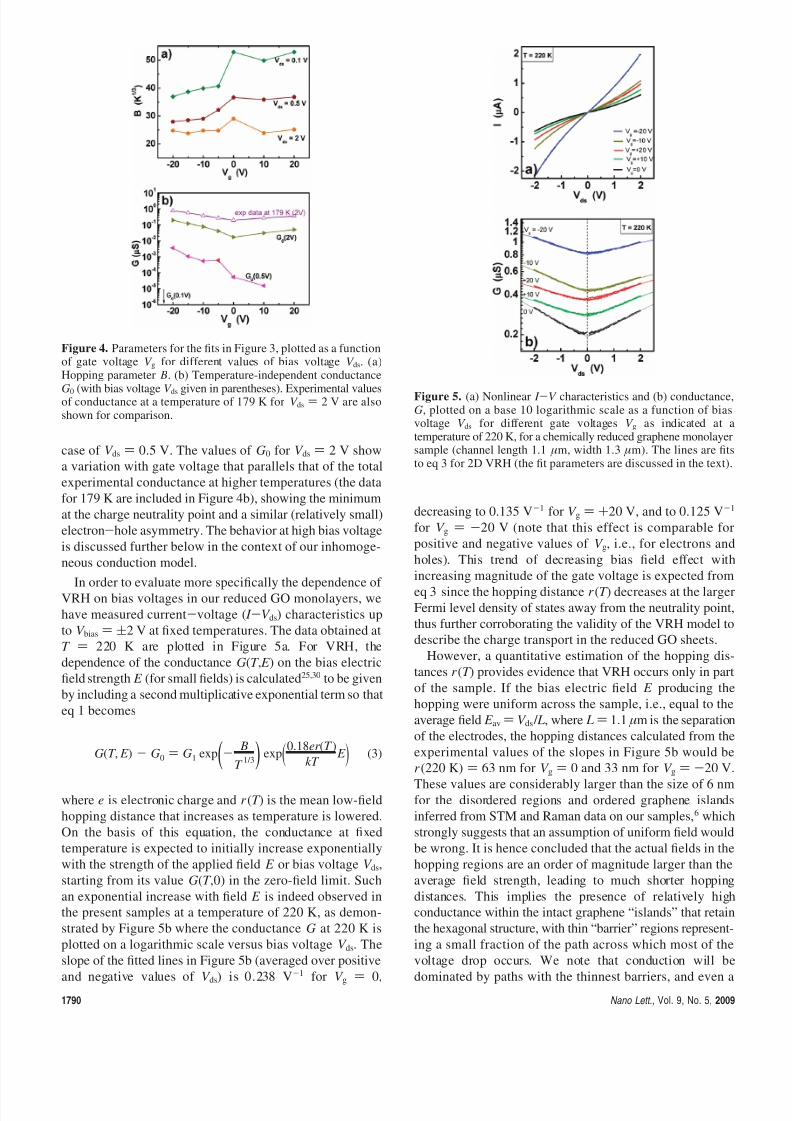
In order to evaluate more specifically the dependence of VRH on bias voltages in our reduced GO monolayers, we
have measured current-voltage ( I -V ds) characteristics up
to V bias ) (2 V at fixed temperatures. The data obtained at
T ) 220 K are plotted in Figure 5a. For VRH, the
dependence of the conductance G(T , E ) on the bias electric
field strength E (for small fields) is calculated25,30 to be given
by including a second multiplicative exponential term so that
eq 1 becomes
where e is electronic charge and r (T ) is the mean low-field
hopping distance that increases as temperature is lowered.
On the basis of this equation, the conductance at fixed
temperature is expected to initially increase exponentially
with the strength of the applied field E or bias voltage V ds,
starting from its value G(T ,0) in the zero-field limit. Such
an exponential increase with field E is indeed observed in
the present samples at a temperature of 220 K, as demon-
strated by Figure 5b where the conductance G at 220 K is
plotted on a logarithmic scale versus bias voltage V ds. The
slope of the fitted lines in Figure 5b (averaged over positive
and negative values of V ds) is 0.238 V
-1
for V g)
0,
decreasing to 0.135 V-1 for V g ) +20 V, and to 0.125 V-1
for V g ) -20 V (note that this effect is comparable for
positive and negative values of V g, i.e., for electrons and
holes). This trend of decreasing bias field effect with
increasing magnitude of the gate voltage is expected from
eq 3 since the hopping distance r (T ) decreases at the largerFermi level density of states away from the neutrality point,
thus further corroborating the validity of the VRH model to
describe the charge transport in the reduced GO sheets.
However, a quantitative estimation of the hopping dis-
tances r (T ) provides evidence that VRH occurs only in part
of the sample. If the bias electric field E producing the
hopping were uniform across the sample, i.e., equal to the
average field E av ) V ds / L, where L ) 1.1 µm is the separation
of the electrodes, the hopping distances calculated from the
experimental values of the slopes in Figure 5b would be
r (220 K) ) 63 nm for V g ) 0 and 33 nm for V g ) -20 V.
These values are considerably larger than the size of 6 nmfor the disordered regions and ordered graphene islands
inferred from STM and Raman data on our samples,6 which
strongly suggests that an assumption of uniform field would
be wrong. It is hence concluded that the actual fields in the
hopping regions are an order of magnitude larger than the
average field strength, leading to much shorter hopping
distances. This implies the presence of relatively high
conductance within the intact graphene “islands” that retain
the hexagonal structure, with thin “barrier” regions represent-
ing a small fraction of the path across which most of the
voltage drop occurs. We note that conduction will be
dominated by paths with the thinnest barriers, and even a
Figure 4. Parameters for the fits in Figure 3, plotted as a functionof gate voltage V g for different values of bias voltage V ds. (a)Hopping parameter B. (b) Temperature-independent conductance
G0 (with bias voltage V ds given in parentheses). Experimental valuesof conductance at a temperature of 179 K for V ds ) 2 V are alsoshown for comparison.
G(T , E ) - G0 ) G1 exp(-B
T 1/3) exp(
0.18er (T )
kT E ) (3)
Figure 5. (a) Nonlinear I -V characteristics and (b) conductance,G, plotted on a base 10 logarithmic scale as a function of biasvoltage V ds for different gate voltages V g as indicated at atemperature of 220 K, for a chemically reduced graphene monolayersample (channel length 1.1 µm, width 1.3 µm). The lines are fitsto eq 3 for 2D VRH (the fit parameters are discussed in the text).
1790 Nano Lett., Vol. 9, No. 5, 2009
7/27/2019 Electrical Conduction Mechanism in Chemically Derived Graphene Monolayers
narrow highly conducting path between ordered “islands”
would short out hopping barrier regions and greatly reduce
the fraction of path where conduction is by hopping.
This scenario is familiar from conduction in highly
conducting polymers, which often consist of crystalline,
metallic regions that are separated by disordered barriers that
dominate the total resistance.21 In the most highly conducting
polymers such as doped polyacetylene, a large fraction of the conduction path is metallic, but the resistance is largely
due to thin barriers (constituting only a few percent of the
path) through which conduction is by fluctuation-assisted
tunneling.31 In this case, since tunneling can occur even in
the zero temperature limit, an appreciable fraction of the
conductance is retained as the temperature approaches zero.
However, as the fraction of disordered polymer is increased,
or the doping level reduced, there is an evolution to VRH
conduction in larger disordered regions and the conductance
decreases to zero in the zero-temperature limit (this latter
case is analogous to the present 2D graphene sheets). An
analogous behavior is also seen in single-wall carbonnanotube (SWCNT) networks, in which conduction is
dominated by metallic tubes but is limited by conduction
barriers formed by intertube contacts and defects along
tubes.32-34 As the thickness of the SWCNT networks is
reduced, there is a change from fluctuation-assisted tunneling
through thin barriers to 2D VRH through thicker barriers
with conductivity extrapolating to zero in the zero-temper-
ature limit.32 The greater effect of disorder in 2D compared
to 3D supports our proposed scenario for the reduced GO
monolayers. Note that metallic-like conduction in ordered
regions (essentially in series with the hopping conduction
in barriers) would contribute a much smaller resistance than
the hopping and thus not significantly affect the temperature
dependence of the total resistance, which at high temperatures
remains characteristic of VRH.
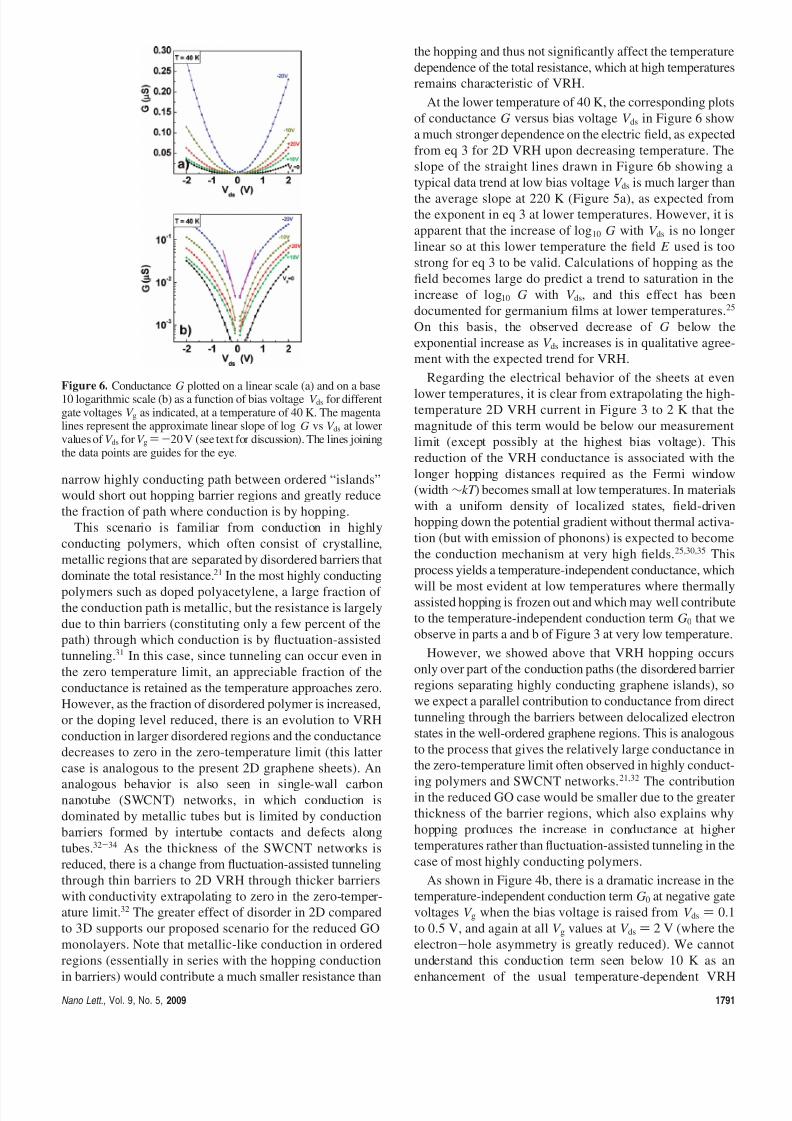
At the lower temperature of 40 K, the corresponding plots
of conductance G versus bias voltage V ds in Figure 6 show
a much stronger dependence on the electric field, as expected
from eq 3 for 2D VRH upon decreasing temperature. The
slope of the straight lines drawn in Figure 6b showing a
typical data trend at low bias voltage V ds is much larger than
the average slope at 220 K (Figure 5a), as expected fromthe exponent in eq 3 at lower temperatures. However, it is
apparent that the increase of log10 G with V ds is no longer
linear so at this lower temperature the field E used is too
strong for eq 3 to be valid. Calculations of hopping as the
field becomes large do predict a trend to saturation in the
increase of log10 G with V ds, and this effect has been
documented for germanium films at lower temperatures.25
On this basis, the observed decrease of G below the
exponential increase as V ds increases is in qualitative agree-
ment with the expected trend for VRH.
Regarding the electrical behavior of the sheets at even
lower temperatures, it is clear from extrapolating the high-temperature 2D VRH current in Figure 3 to 2 K that the
magnitude of this term would be below our measurement
limit (except possibly at the highest bias voltage). This
reduction of the VRH conductance is associated with the
longer hopping distances required as the Fermi window
(width∼kT ) becomes small at low temperatures. In materials
with a uniform density of localized states, field-driven
hopping down the potential gradient without thermal activa-
tion (but with emission of phonons) is expected to become
the conduction mechanism at very high fields.25,30,35 This
process yields a temperature-independent conductance, which
will be most evident at low temperatures where thermallyassisted hopping is frozen out and which may well contribute
to the temperature-independent conduction term G0 that we
observe in parts a and b of Figure 3 at very low temperature.
However, we showed above that VRH hopping occurs
only over part of the conduction paths (the disordered barrier
regions separating highly conducting graphene islands), so
we expect a parallel contribution to conductance from direct
tunneling through the barriers between delocalized electron
states in the well-ordered graphene regions. This is analogous
to the process that gives the relatively large conductance in
the zero-temperature limit often observed in highly conduct-
ing polymers and SWCNT networks.21,32
The contributionin the reduced GO case would be smaller due to the greater
thickness of the barrier regions, which also explains why
hopping produces the increase in conductance at higher
temperatures rather than fluctuation-assisted tunneling in the
case of most highly conducting polymers.
As shown in Figure 4b, there is a dramatic increase in the
temperature-independent conduction term G0 at negative gate
voltages V g when the bias voltage is raised from V ds ) 0.1
to 0.5 V, and again at all V g values at V ds ) 2 V (where the
electron-hole asymmetry is greatly reduced). We cannot
understand this conduction term seen below 10 K as an
enhancement of the usual temperature-dependent VRH
Figure 6. Conductance G plotted on a linear scale (a) and on a base10 logarithmic scale (b) as a function of bias voltage V ds for differentgate voltages V g as indicated, at a temperature of 40 K. The magentalines represent the approximate linear slope of log G vs V ds at lowervalues of V ds for V g ) -20 V (see text for discussion). The lines joiningthe data points are guides for the eye.
Nano Lett., Vol. 9, No. 5, 2009 1791
7/27/2019 Electrical Conduction Mechanism in Chemically Derived Graphene Monolayers
270–274.(10) Li, D.; Muller, M. B.; Gilje, S.; Kaner, R. B.; Wallace, G. G. Nat.
Nanotechnol. 2008, 3 (2), 101–105.(11) Wang, X.; Zhi, L. J.; Mullen, K. Nano Lett. 2008, 8 (1), 323–327.(12) Stankovich, S.; Dikin, D. A.; Dommett, G. H. B.; Kohlhaas, K. M.;
Zimney, E. J.; Stach, E. A.; Piner, R. D.; Nguyen, S. T.; Ruoff, R. S.
Nature (London) 2006, 442 (7100), 282–286.(13) Watcharotone, S.; A, D. D.; Stankovich, S.; P., R.; Jung, I.; Dommett,
G. H.B.; E, G.; W., S.-E.; C., S.-F.; L., C.-P.; N., S. T.; S., R. R.
Nano Lett. 2007, 7 (7), 1888–1892.(14) Weng, L. S.; Zhang, L. Y.; Chen, Y. P.; Rokhinson, L. P. Appl. Phys.
Lett. 2008, 93 (9), xx.(15) Giesbers, A. J. M.; Zeitler, U.; Neubeck, S.; Freitag, F.; Novoselov,
K. S.; Maan, J. C. Solid State Commun. 2008, 147 (9-10), 366–369.(16) Stankovich, S.; Dikin, D. A.; Piner, R. D.; Kohlhaas, K. A.;
Kleinhammes, A.; Jia, Y.; Wu, Y.; Nguyen, S. T.; Ruoff, R. S. Carbon
2007, 45 (7), 1558–1565.(17) Tuinstra, F.; Koenig, J. L. J. Chem. Phys. 1970, 53 (3), 1126–&.(18) Jung, I.; Dikin, D. A.; Piner, R. D.; Ruoff, R. S. Nano Lett. 2008, 8,
4283–4287.(19) Gilje, S.; Han, S.; Minsheng, W.; Kang, L. W.; Kaner, R. B. Nano
Lett. 2007, 7 (11), 3394–3398.(20) Wu, X. S.; Sprinkle, M.; Li, X.; Fan, M.; Berger, C.; De Heer, W. A.
Phys. ReV. Lett. 2008, 101, 026801.(21) Kaiser, A. B. Ad V. Mater. 2001, 13 (12-13), 927–939.(22) Hummers, W. S.; Offeman, R. E. J. Am. Chem. Soc. 1958, 80 (6),
1339–1339.(23) Anwar, A.; Nabet, B.; Culp, J.; Castro, F. J. Appl. Phys. 1999, 85 (5),
2663–2666.(24) Bockrath, M.; Cobden, D. H.; Lu, J.; Rinzler, A. G.; Smalley, R. E.;
Balents, T.; McEuen, P. L. Nature (London) 1999, 397 (6720), 598–
601.(25) Mott, N. F.; A. Davis, E. Electronic Processes in Non-Crystalline
Materials, 2nd ed.; Oxford University Press: Oxford, England, 1979.(26) Huard, B.; Stander, N.; Sulpizio, J. A.; Goldhaber-Gordon, D. Phys.
ReV. B 2008, 78 (12), xx.(27) Farmer, D. B.; Golizadeh-Mojarad, R.; Perebeinos, V.; Lin, Y. M.;
Tulevski, G. S.; Tsang, J. C.; Avouris, P. Nano Lett. 2009, 9 (1), 388–
392.(28) Novikov, D. S. Appl. Phys. Lett. 2007, 91 (10), xx.(29) Chen, J. H.; Jang, C.; Adam, S.; Fuhrer, M. S.; Williams, E. D.;
Ishigami, M. Nat. Phys. 2008, 4 (5), 377–381.
(30) Pollak, M.; Riess, I. J. Phys. C: Solid State Phys. 1976, 9 (12), 2339–2352.
(31) Sheng, P. Phys. ReV. B 1980, 21 (6), 2180–2195.(32) Skakalova, V.; Kaiser, A. B.; Woo, Y. S.; Roth, S. Phys. ReV. B 2006,
74 (8), xx.(33) Kaiser, A. B. Rep. Prog. Phys. 2001, 64 (1), 1–49.(34) Gruner, G. J. Mater. Chem. 2006, 16 (35), 3533–3539.(35) Shklovskii, B. I. SoV. Phys. Semiconduct. 1973, 6 (12), 1964–1967.