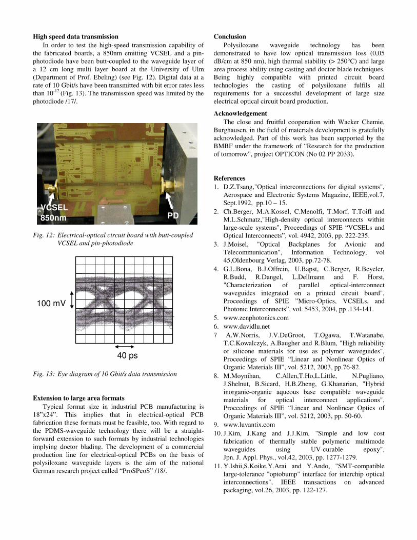
Electrical-Optical Circuit Board Using Polysiloxane Optical Waveguide Layer
A. Neyer, S. Kopetz, E. Rabe, W.J. Kang, S. Tombrink
Universität Dortmund, Fakultät für Elektrotechnik und Informationstechnik,
Arbeitsgebiet Mikrostrukturtechnik (AG MST)
44221 Dortmund, Tel.: ++49 231 755 3728, Fax.: ++49 231 755 3729,
e-mail: [email protected]
Abstract
This paper reports on a new technology for the realization
of an optical waveguide layer in electrical-optical circuit
boards. The technology is based on casting of transparent
polysiloxanes as low cost, low loss (0,05 dB/cm at 850 nm)
and high temperature stable (> 250°C) material system. The
waveguide layer fabrication will be discussed as well as the
preparation of suitable casting moulds. Further issues are the
material and waveguide properties of optical polysiloxanes,
the coupling to OE-modules, and the lamination of optical
layers into printed circuit boards.
Introduction
Next-generation internet switches and high-end computers
are expected to process aggregate data rates in the order of
Tbit/s. In consequence, the interconnections between the
processing units will have to handle data rates in the order of
10-40 Gbit/s. It is, however, well known from basic physical
laws that electrical interconnections will suffer from high
transmission losses and severe signal integrity problems at
such data rates /1/. In order to overcome the evident high-
speed interconnection bottle-neck, optical interconnects are
considered the preferred option. In Gbit/s-rack-to-rack
interconnections with link lengths in the order of several
meters, the widespread solution is the commercial fibre-ribbon
cable in combination with high speed parallel OE-modules. If,
however, interconnection lengths come down to the order of
1m, e.g. in backplanes, integrated optical waveguides are
considered more economical /2/.
The integration of optical waveguides in printed circuit
boards as well as in backplanes imposes severe requirements
on the materials and processes involved. Some of them are:
High transparency of the waveguide materials (< 0,1dB/cm) in
the standardized interconnect wavelength window of 850 nm,
high temperature stability to overcome standard multilayer
printed circuit board lamination process temperatures at
180°C for two hours and especially the soldering process
temperatures of 230°C, large area processing capability (>
0,5m x 0,5m), and cost effective mass production.
Among the waveguide technologies studied worldwide for
the production of electrical-optical PCBs, photolithography is
the most popular to define the multimode waveguide core
structure. Both, direct laser writing /3/ and mask exposure
techniques /4/ are being applied. A considerable variety of
temperature stable polymers have been developed for this
technology: modified acrylates /4,5/, polysiloxanes /6,7,8/,
and epoxies / 9,10,11/.
Waveguide data obtained with theses techniques and materials
are summarized in Table I.
Company Material Thermal
stability
°C
Optical loss
at 850nm
dB/cm
Luvantix /9/ Epoxy >250 0,04
KIST /10/ Epoxy 220 0,36
NTT /11/ Epoxy >200 0,1
Zen
Photonics /5/
Acrylate >250 0,05
IBM /4/ Acrylate >250 0,04
Daimler
Chrysler /3/
Unknown >250 0,04
RPO /6/ Siloxane >250 0,1
Dow
Corning/7/
Siloxane >200 0,06
Shipley /8/ Siloxane >250 <0,1
Table I: Performance data of multimode waveguides
fabricated by photolithographic methods
Although the photopolymer waveguides reported in Table
I show excellent performance their implementation in large
area boards is critical because of the high material costs.
Furthermore, hot embossing has been investigated as a
suitable technology for multimode polymer waveguide
fabrication /12,13/. However, problems may arise from
insufficient high temperature stability of optical thermoplastic
polymers (for T>200°C) as well as from difficulties with the
required high precision at large areas.
In this paper we present a new waveguide technology
based on casting of thermally curing polysiloxanes which
comprises all essential features for a low cost mass production
of large area electrical-optical circuit boards.
Materials
High transparent polysiloxanes are widely used in
electronics industries, e.g. to encapsulate LEDs. In addition to
the low optical loss, the advantages of polysiloxane for
integrated optical waveguide fabrication in printed circuit
boards are the high thermal stability, the extreme moulding
precision, the large area process ability and especially the low
cost.
Fig. 1: High replication precision in PDMS:
Moulded Y-splitter
The transmission loss of optical grade polysiloxane bulk
samples of different suppliers has been measured to 0,02 -
0,04 dB/cm in the 850 nm wavelength window.
0
0,1
0,2
0,3
0,4
0,5
0,6
300 800 1300 1800
Wavelength [nm]
Pro
pag
ati
on
lo
ss [
dB
/cm
]
0,03dB/cm@850nm
Fig. 2: Spectral transmission of bulk PDMS (Wacker)
In this paper, two-component room temperature cross
linking polysiloxanes of Wacker Chemie GmbH, Burghausen,
Germany, have been used. The cladding materials are standard
commercial polymers, whereas the core polymer is a special
development of Wacker in close cooperation with the
University of Dortmund. The transmission spectra of core and
cladding materials are almost identical (Fig. 2)
The thermal stability of the polysiloxane materials has
been studied by comparing the transmission spectra of bulk
samples after curing them at room temperature, after a
subsequent exposure at 180°C for two hours and after a final
exposure at 230°C for five minutes (Fig. 3). This temperature
treatment simulates the real process conditions at multilayer
board lamination and at reflow soldering. Except in the
ultraviolet region (200 nm to 400 nm) there is no significant
change in the optical transmission loss. A slight increase in
transmission loss is observed only at temperatures above
270°C which makes the material very suitable even for lead
free soldering processes.
0
1
2
3
4
5
6
7
8
9
10
200 700 1200 1700
Wavelenght [nm]
Insert
ion loss [d
B/c
m]
20°C
180°C
250°C
Fig.3: Thermal stability of PDMS
Fabrication of waveguide layer and board integration
Reactive ion etching and UV-curing have been reported
for waveguide fabrication in polysiloxane /14,15/. We have
adopted casting in combination with the doctor blade
technique as a new low cost polysiloxane waveguide
fabrication method. One of the advantages of this technology
is that it has the unique feature of simultaneous fabrication of
optical waveguides together with integrated micro mirrors for
efficient OE-module coupling. Furthermore, casting in
combination with the doctor blade technique is well
compatible with large area printed circuit board production
technologies.
First a casting mould for the waveguide core layer is
generated. This is accomplished by SU-8-photolithography
and subsequent electroplating. In the reported experiments
standard 6”-photoresist technology has been applied, but
currently extension to larger formats (300mm x 400mm) is
under work. In case of large area formats, doctor blading is
used instead of spin coating because of the better thickness
uniformity of the resist on rectangular substrates. The resist is
dried and exposed through a photolithographic mask. After
development of the resist the master mould is finished (Fig. 4).
In order to obtain a mechanical stable mould for mass
production an electroplated copy of the resist mould is
realized.
Fig. 4: SU-8 master form with straight waveguides
The complete production process of the optical layer is
shown in Fig. 5.
core polymer
mould
mould
Substrate carrier
substratepolymer
substrate
substrate carrier
waveguide cores
mould
waveguide cores
Substrate
pressing,
curing
Application of core polymer
Doctor blading,
curing
Demoulding
Superstrate
pressing,
curing
superstrate
polymer
substrate
waveguide coressuperstrate carrier
core polymer
mouldmould
mould
Substrate carrier
substratepolymer
substrate
substrate carrier
waveguide cores
mould
waveguide cores
mould
waveguide cores
Substrate
pressing,
curing
Application of core polymer
Doctor blading,
curing
Demoulding
Superstrate
pressing,
curing
superstrate
polymer
substrate
waveguide coressuperstrate carrier
Fig. 5: Scheme of production process of optical layer
First, the waveguide cores are fabricated by filling the
grooves in the mould by the core polymer (n = 1.43). This is
accomplished by the doctor blading technique which is easily
applicable to large formats. Then the core material is
thermally cured.
The next step is the preparation of the substrate carrier.
One function of this carrier is the mechanical stabilisation of
the thin optical layer during the subsequent production steps.
At the same time, the carrier serves as interface to adjacent
PCB layers in case of a multi layer board. It is obvious to use
conventional circuit board laminates like FR4 or Kapton. It is
advantageous to use copper clad material, since the copper can
be structured by standard processes and these structures are
well suited to define the thickness of the substrate polymer.
Another function of the copper structures is the prevention of
pressure from the waveguide layer during multilayer PCB
lamination.
The waveguide substrate layer is fabricated by applying
the liquid cladding polymer (n=1.41) to the mould (which still
contains the cured cores) and, subsequently, the substrate
carrier is pressed against the mould. Now, the copper
structures will define exactly the thickness of the waveguide
substrate layer. After curing the complete layer comprising
cores, substrate layer and carrier is demoulded. Excellent
adhesion between the substrate carrier and the PDMS
substrate layer could be achieved by using special adhesion
promoters.
The production of the superstrate layer is performed by the
same technique using identical cladding polymer (n = 1.41)
and a superstrate carrier with copper structures to define the
thickness of the superstrate layer
Fig. 6 shows the cross section of a realized electrical-
optical PCB using FR4 substrate carriers. The waveguides
have core sizes of 70µm x 70µm and a numerical aperture of
0.26.
Fig. 6 Cross section of PDMS optical layer
embedded between FR4 laminates
An alternative carrier material in particular with regard to
flexible board applications or very high temperature stability
is the polyimide film Kapton® (Dupont). In Fig. 7 the cross
section of such a laminate with Kapton® is shown.
Fig. 7: Cross section of PDMS optical layer
embedded between Kapton laminates
Kapton
Kapton
Superstrate
Substrate
Waveguide core
FR4
Substrate
Superstrate
Waveguide core
Transmission loss and thermal stability
The waveguide loss has been measured by exciting the
waveguides using a 50µm-GI-fibre and collecting the
transmitted light by a 200µm-SI-fibre. Typical waveguide loss
figures at 850 nm are 0,05 dB/cm measured by the cut back
method.(see Fig. 8) The thermal stability has been tested
against the PCB-lamination temperature at 180°C for 2 hours
followed by an exposure at 230°C for 5 minutes to simulate
reflow soldering conditions. Fig. 8 shows the results of these
thermal stability tests.
0,00
0,01
0,02
0,03
0,04
0,05
0,06
0,07
0,08
1 2 3 4 5 6 7 8 9 10 11 12Waveguide number
Pro
pag
ati
on
lo
ss [
dB
/cm
]
Before annealing
180°C 2h
220°C 5 min
Fig. 8: Thermal stability of PDMS waveguide layer
If embedded between two Kapton carriers the optical
waveguide could be annealed up to 260°C without observable
increase of the optical loss. There is even a tendency of
improvement of the optical transmission after the exposure to
higher temperatures.
0,00
0,02
0,04
0,06
0,08
0,10
0,12
0,14
1 2 3 4 5 6 7 8 9 10
Waveguide number
Pro
pag
ati
on
lo
ss [
dB
/cm
] Before annealing
180°C 2h
220°C 5m
260°C 5m
Fig. 9: PMDS waveguides embedded between two Kapton
carriers (see Fig. 7)
Coupling to OE-modules
Besides the integration of an optical waveguide layer in a
PCB, the optical coupling in and out of the board is of crucial
importance for the success of the concept of optical
interconnections in PCBs. In this paper a micro mirror
technology is proposed /16/ which is well compatible to the
described replication process. The basic idea is to realize the
mirror structures already at the masterform level and apply the
waveguide layer fabrication as outlined.
The micro mirrors are integrated into the masterform at
the SU-8 resist level by micro milling the end faces of the
cured SU-8 ridges under an angle of 45° (Fig. 10). Cured SU-
8 is a very suitable material to be treated by micro milling. To
obtain optimum results with respect to surface roughness of
the mirrors, specially designed diamond milling tools have
been developed. The obtained roughness on the mirror surface
has been measured by white-light interferometry to Ra=70-
80nm which is an acceptable value.
Main drawback of the integrated micro mirror technology
is the need to metallise each replicated waveguide substrate
locally at the mirror positions. Furthermore, a transmission
window must be opened in the superstrate carrier and the top
layer of the board (see Fig. 11) .
Fig. 10: SEM-photo of milled micro mirrors
Fig. 11: Waveguides with integrated micromirrors
and MT–pins for passive OE-module coupling
High speed data transmission
In order to test the high-speed transmission capability of
the fabricated boards, a 850nm emitting VCSEL and a pin-
photodiode have been butt-coupled to the waveguide layer of
a 12 cm long multi layer board at the University of Ulm
(Department of Prof. Ebeling) (see Fig. 12). Digital data at a
rate of 10 Gbit/s have been transmitted with bit error rates less
than 10-12
(Fig. 13). The transmission speed was limited by the
photodiode /17/.
Fig. 12: Electrical-optical circuit board with butt-coupled
VCSEL and pin-photodiode
Fig. 13: Eye diagram of 10 Gbit/s data transmission
Extension to large area formats
Typical format size in industrial PCB manufacturing is
18”x24”. This implies that in electrical-optical PCB
fabrication these formats must be feasible, too. With regard to
the PDMS-waveguide technology there will be a straight-
forward extension to such formats by industrial technologies
implying doctor blading. The development of a commercial
production line for electrical-optical PCBs on the basis of
polysiloxane waveguide layers is the aim of the national
German research project called “ProSPeoS” /18/.
Conclusion
Polysiloxane waveguide technology has been
demonstrated to have low optical transmission loss (0,05
dB/cm at 850 nm), high thermal stability (> 250°C) and large
area process ability using casting and doctor blade techniques.
Being highly compatible with printed circuit board
technologies the casting of polysiloxane fulfils all
requirements for a successful development of large size
electrical optical circuit board production.
Acknowledgement
The close and fruitful cooperation with Wacker Chemie,
Burghausen, in the field of materials development is gratefully
acknowledged. Part of this work has been supported by the
BMBF under the framework of “Research for the production
of tomorrow”, project OPTICON (No 02 PP 2033).
References
1. D.Z.Tsang,"Optical interconnections for digital systems",
Aerospace and Electronic Systems Magazine, IEEE,vol.7,
Sept.1992, pp.10 – 15.
2. Ch.Berger, M.A.Kossel, C.Menolfi, T.Morf, T.Toifl and
M.L.Schmatz,"High-density optical interconnects within
large-scale systems", Proceedings of SPIE “VCSELs and
Optical Interconnects”, vol. 4942, 2003, pp. 222-235.
3. J.Moisel, "Optical Backplanes for Avionic and
Telecommunication", Information Technology, vol
45,Oldenbourg Verlag, 2003, pp.72-78.
4. G.L.Bona, B.J.Offrein, U.Bapst, C.Berger, R.Beyeler,
R.Budd, R.Dangel, L.Dellmann and F. Horst,
"Characterization of parallel optical-interconnect
waveguides integrated on a printed circuit board",
Proceedings of SPIE ”Micro-Optics, VCSELs, and
Photonic Interconnects”, vol. 5453, 2004, pp .134-141.
5. www.zenphotonics.com
6. www.davidlu.net
7 A.W.Norris, J.V.DeGroot, T.Ogawa, T.Watanabe,
T.C.Kowalczyk, A.Baugher and R.Blum, "High reliability
of silicone materials for use as polymer waveguides",
Proceedings of SPIE “Linear and Nonlinear Optics of
Organic Materials III”, vol. 5212, 2003, pp.76-82.
8. M.Moynihan, C.Allen,T.Ho,L.Little, N.Pugliano,
J.Shelnut, B.Sicard, H.B.Zheng, G.Khanarian, "Hybrid
inorganic-organic aqueous base compatible waveguide
materials for optical interconnect applications",
Proceedings of SPIE “Linear and Nonlinear Optics of
Organic Materials III”, vol. 5212, 2003, pp. 50-60.
9. www.luvantix.com
10. J.Kim, J.Kang and J.J.Kim, "Simple and low cost
fabrication of thermally stable polymeric multimode
waveguides using UV-curable epoxy",
Jpn. J. Appl. Phys., vol.42, 2003, pp. 1277-1279.
11. Y.Ishii,S.Koike,Y.Arai and Y.Ando, "SMT-compatible
large-tolerance "optobump" interface for interchip optical
interconnections", IEEE transactions on advanced
packaging, vol.26, 2003, pp. 122-127.
40 ps
100 mV
VCSEL
850nm PD
12. S. Lehmacher and A.Neyer, “Integration of polymer
optical waveguides into printed circuit boards", Electron.
Lett., vol. 36, 2000, pp. 1052-1053
13. D. Krabe, W. Scheel, “Optical interconnects by hot
embossing for module and PCB technology – The EOCB
approach,” Proceedings of 49th Electronics Components
& Technology Conference, San Diego, USA, June 1999,
pp. 1164-1166
14. Usui, M., Hikata, M., Watanabe, T., Amano, M.,
Sugawara, S., Hayashida, S. and Imamura, S., "Low–loss
passive polymer waveguides with high environmental
stability”, Journal of Lightwave Technology, 1996, vol. 14
no. 10 pp.2338-2343.
15. US Patent Application: Polymer waveguides and process
for producing the same, Pub. No.: US 2002/0150368 A1,
2002
16. S. Kopetz, S. Lehmacher, E. Rabe, and A. Neyer,
" Coupling of optoelectronic modules to the optical layer
in printed circuit boards", Proc. of SPIE Photonics
Fabrication Europe, Brugge, Belgium, 2002
17. A. Neyer, S. Kopetz, E. Rabe, W.J. Kang, M. Stach and R.
Michalzik , "10 Gbit/s Electrical-Optical Circuit Board
Based on New Polysiloxane Waveguide Technology" ,
Proceedings of the ECOC 2004, Stockholm, Sweden, 2004
18. www.prospeos.de