53
STUDENTS’ SPACE ASSOCIATION THE FACULTY OF POWER AND AERONAUTICAL ENGINEERING WARSAW UNIVERSITY OF TECHNOLOGY CRITICAL DESIGN REVIEW Electrical Power System November 2016 Issue no. 1
STUDENTS’ SPACE ASSOCIATION
THE FACULTY OF POWER AND AERONAUTICAL ENGINEERING
WARSAW UNIVERSITY OF TECHNOLOGY
CRITICAL DESIGN REVIEW
Electrical Power System
November 2016
Issue no. 1

PW-Sat2 Critical Design Review
2016-11-30 Electrical Power System
Phase C
pw-sat.pl
1 of 53
Changes
Date Changes Pages/Section Responsible
2016-02-18 Phase B documentation review Phase B - EPS PDR document Sławosz Uznański
2016-11-30 First issue of the document Whole document
Microcontroller selection
Piotr Kuligowski
Grzegorz Gajoch
Published by
Students’ Space Association
Warsaw University of Technology, 2016
This work is licensed on CC BY-NC 3.0
Project logo by Krzysztof Karaś
Artist’s impressions by Marcin Świetlik
Quote as: PW-Sat2 Team, Phase C Documentation – Critical Design Review – Electrical Power System,
Students’ Space Association, Warsaw University of Technology, pw-sat.pl 2016

PW-Sat2 Critical Design Review
2016-11-30 Electrical Power System
Phase C
pw-sat.pl
2 of 52
Table of contents
1 Introduction 9
1.1 Purpose and Scope .................................................................................................................................... 9
1.2 Reference Documents ............................................................................................................................... 9
1.3 Document Contributors ........................................................................................................................... 10
1.4 Documentation review ............................................................................................................................ 10
2 System requirements 11
2.1 Possibility of connection of 4 solar panels .............................................................................................. 11
2.2 MPPT tracking ........................................................................................................................................ 12
2.3 Energy storage ........................................................................................................................................ 12
2.4 Redundancy of critical sections .............................................................................................................. 12
2.5 Possibility of supplying subsystems directly from solar panels .............................................................. 13
2.6 Possibility of manually disconnection of accumulators using RBL ........................................................ 13
2.7 Deployment switch ................................................................................................................................. 13
2.8 Two controllers for redundancy .............................................................................................................. 14
2.9 LCL for each subsystem ......................................................................................................................... 15
2.10 Creating voltages 3.3V, 5V and ACC ..................................................................................................... 15
2.10.1 Required voltages for each subsystem ........................................................................................ 15
2.11 Emergency disconnection when low battery ........................................................................................... 16
2.12 Running in space environment ................................................................................................................ 16
2.13 Currents and voltages monitoring ........................................................................................................... 16
2.14 Requirements for the PCB ...................................................................................................................... 17
2.14.1 Dimensions of the PCB ............................................................................................................... 17
2.14.2 PCB procurement ....................................................................................................................... 18
2.15 Electromagnetic compatibility ................................................................................................................ 18
3 EPS design 19
3.1 MPPT regulators ..................................................................................................................................... 19
3.1.1 ORing diodes for solar panels ......................................................................................................... 21
3.1.2 Input EMI filters .............................................................................................................................. 22

PW-Sat2 Critical Design Review
2016-11-30 Electrical Power System
Phase C
pw-sat.pl
3 of 52
3.1.3 I and V measurements ..................................................................................................................... 23
3.1.4 Controlled DCDC converter ........................................................................................................... 23
3.1.5 ORing diodes to MPB ...................................................................................................................... 24
3.2 Battery controller .................................................................................................................................... 24
3.3 Kill-switch circuit ................................................................................................................................... 25
3.4 Remove before launch circuit ................................................................................................................. 26
3.5 DCDC converters for 3V3 and 5V .......................................................................................................... 26
3.6 Internal supply ........................................................................................................................................ 28
3.7 Controllers............................................................................................................................................... 29
3.7.1 Controller A .................................................................................................................................... 29
3.7.2 Controller B .................................................................................................................................... 30
3.8 Distribution ............................................................................................................................................. 31
4 Components selection 34
4.1 Microcontroller selection ........................................................................................................................ 34
4.1.1 Requirements ................................................................................................................................... 34
4.1.2 Part selection .................................................................................................................................. 34
4.1.3 Radiation effect analysis in ATMega ............................................................................................... 36
4.1.4 ATMega selection conclusion .......................................................................................................... 38
4.1.5 Programming ATMega microcontroller .......................................................................................... 38
5 Current state of work 40
5.1 EM1 model.............................................................................................................................................. 40
5.1.1 EM1 sub-modules ............................................................................................................................ 41
5.1.2 EM1 software development ............................................................................................................. 43
5.1.3 EM1 tests results ............................................................................................................................. 44
5.2 EM2 model.............................................................................................................................................. 48
6 Tests plan for EM2 49
6.1 Kill-Switches ........................................................................................................................................... 49
6.2 EMC - radiation susceptibility ................................................................................................................ 49
6.3 EMC – conducted emission .................................................................................................................... 50
6.4 EMC – phase margins for DCDC converters .......................................................................................... 51

PW-Sat2 Critical Design Review
2016-11-30 Electrical Power System
Phase C
pw-sat.pl
4 of 52
7 EPS EGSE 52

PW-Sat2 Critical Design Review
2016-11-30 Electrical Power System
Phase C
pw-sat.pl
5 of 52
List of figures
Figure 1-1 Functional block diagram of the system ................................................................................................................... 9
Figure 2-1. Functional block diagram of the system ................................................................................................................ 11
Figure 2-2. An example of the RBF – KySat1 from Kentucky Space ...................................................................................... 13
Figure 2-3. Placement for deployment switches – source [1] ................................................................................................... 14
Figure 2-4. Deployment switch - surce TISAT-1 ..................................................................................................................... 14
Figure 2-5. Top and side view of the PCB ............................................................................................................................... 17
Figure 2-6. Bottom view of the PCB ........................................................................................................................................ 18
Figure 3-1 Simplified block diagram ........................................................................................................................................ 19
Figure 3-2 Solar panels Y+, Y- and X+ - source [PW-Sat2-C-10.00-CONF-CDR] ................................................................. 20
Figure 3-3 Solar panels X- - source [PW-Sat2-C-10.00-CONF-CDR] .................................................................................... 20
Figure 3-4 MPPT regulators ..................................................................................................................................................... 21
Figure 3-5 Oring diodes and EMI filters for solar panels X+ and X- ....................................................................................... 21
Figure 3-6 Oring diodes and EMI filters for solar panels Y+ and Y- ....................................................................................... 22
Figure 3-7 EMI filters for solar panels X+ and X- ................................................................................................................... 22
Figure 3-8 EMI filters for solar panels Y+ and Y- ................................................................................................................... 23
Figure 3-9 MPPT measurements .............................................................................................................................................. 23
Figure 3-10 Boost converter for MPPT X ................................................................................................................................ 24
Figure 3-11 ORing diodes to MPB ........................................................................................................................................... 24
Figure 3-12 Power stage for battery controller ......................................................................................................................... 25
Figure 3-13. Placement for deployment switches – source [PW-Sat2-C-10.00-CONF-CDR] ................................................. 25
Figure 3-14 Separation switch – source TME.eu...................................................................................................................... 26
Figure 3-15 Remove before launch placement – source [PW-Sat2-C-10.00-CONF-CDR] ..................................................... 26
Figure 3-16 3V3 and 5V DCDC converters for subsystems ..................................................................................................... 27
Figure 3-17 Input and output filters for 3V3 and 5V DCDC converters .................................................................................. 27
Figure 3-18 3V3 DCDC converter ........................................................................................................................................... 28
Figure 3-19 Internal supply ...................................................................................................................................................... 28
Figure 3-20 A single internal supply circuit ............................................................................................................................. 29
Figure 3-21 ATMega325 [6] - Controller A ............................................................................................................................. 30
Figure 3-22 ATMega164 [7] - Controller B ............................................................................................................................. 31
Figure 3-23 Distribution for 3V3 lines ..................................................................................................................................... 32
Figure 3-24 Distribution for 5V lines ....................................................................................................................................... 32
Figure 3-25 Distribution for VBAT lines ................................................................................................................................. 32
Figure 3-26 Distribution detailed block diagram ...................................................................................................................... 33
Figure 4-1. SEE in 2048 bytes of SRAM – source [8] ............................................................................................................. 38
Figure 5-1 Models pholosophy ................................................................................................................................................. 40
Figure 5-2 Simplified block diagram of the EM1 model .......................................................................................................... 41
Figure 5-3 EM1 model - boost converter for MPPT X ............................................................................................................. 41
Figure 5-4 EM1 model - Ideal diode for solar panels and MPB ORing ................................................................................... 42
Figure 5-5 EM1 - RBL and Kill-Switches ................................................................................................................................ 42
Figure 5-6 EM1 model - battery controller ............................................................................................................................... 43
Figure 5-7 EPS on Github ........................................................................................................................................................ 44

PW-Sat2 Critical Design Review
2016-11-30 Electrical Power System
Phase C
pw-sat.pl
6 of 52
Figure 5-8 EM1 measurements setup ....................................................................................................................................... 44
Figure 5-9 Battery pack deep discharge ................................................................................................................................... 45
Figure 5-10 EM1 battery pack charging/discharging cycles .................................................................................................... 46
Figure 5-11 Solar panels simulator for MPPT X ...................................................................................................................... 46
Figure 5-12 EM1 - MPPT X performance ................................................................................................................................ 47
Figure 5-13 EM1 stability measurements ................................................................................................................................. 48
Figure 5-14 EM1 MPPTX bode plot ........................................................................................................................................ 48
Figure 6-1 Kill-Swtches test ..................................................................................................................................................... 49
Figure 6-2 EMC - radiation susceptibility ................................................................................................................................ 50
Figure 6-3 EMC - conducted emission @ inputs ...................................................................................................................... 50
Figure 6-4 EMC - conducted emission @ outputs .................................................................................................................... 51
Figure 6-5 DCDC stability measurements ................................................................................................................................ 51
Figure 7-1 EPS EGSE .............................................................................................................................................................. 52
List of tables
Table 2-1. Required voltages for each subsystem .................................................................................................................... 16
Table 2-2. PCB stack layers from the Techno Service company .............................................................................................. 18
Table 4-1. An example of ATMega part code .......................................................................................................................... 34
Table 4-2. ATMEGA164P-B15AZ – automotive series .......................................................................................................... 35
Table 4-3. ATMega16 review .................................................................................................................................................. 35
Table 4-4. ATMega164 review ................................................................................................................................................ 36
Table 4-5. ATMega168 review ................................................................................................................................................ 36

PW-Sat2 Critical Design Review
2016-11-30 Electrical Power System
Phase C
pw-sat.pl
7 of 52
Abbreviated terms
2U 2-Unit
ACC ACC power bus
ADC Analogue-to-Digital Converter
ADCS Attitude Determination and Control System
CAM Cameras
CAN Controller Area Network – CAN bus
CC-CV Constant Current – Constant Voltage
COMM Communication System
COTS Commercial off-the-shelf
CRC Cyclic Redundancy Check
DAC Digital-to-Analogue Converter
DCDC DC-to-DC converter. It converts one voltage level to another
DoD Depth of Discharge factor
DT Deployment Team
ECC Error-Correcting Code
ECSS European Cooperation for Space Standardization
EGSE Electrical Ground Support Equipment
EM Engineering Model
EMC Electromagnetic Compatibility
EMI Electromagnetic Interferences
EPS Electrical Power System
ESA European Space Agency
ESD Electrostatic Discharge
FBK Feedback
FDIR Fault Detection, Isolation and Recovery
FM Flight Model
FRAM Ferroelectric Random-Access Memory
GND Ground - the reference point in an electrical circuit
GS Ground Station
I2C Inter-Integrated Circuit bus
IC Integrated Circuit
IEEE Institute of Electrical and Electronics Engineers
ISP In-system programming
JAXA Japan Aerospace Exploration Agency
JTAG Joint Test Action Group - IC debug port
LCL Latch-up Current Limiter
LDO Low-Drop-Out regulator
LEO Low Earth Orbit
LET Linear Energy Transfer Threshold
LISN Line Impedance Stabilization Network
LPF Low Pass Filter
MA Mission Analysis
MBS Main Power Bus
MLI Multi-Layer Insulation
MP Military Plastic grade (Linear Technology)
MPB Main Power Bus
MPPT Maximum Power Point Tracking
NASA National Aeronautics and Space Administration
PW-Sat2 Critical Design Review
2016-11-30 Electrical Power System
Phase C
pw-sat.pl
8 of 52
NC Normal Closed (a contact of a switch)
NO Normal Open (a contact of a switch)
OBC On-board Computer
P&O Perturb & Observe algorithm is used for maximum point tracking in PV systems
PCB Printed Circuit Board
PE Local earthing system
PFM Proto-flight Model
PLD Payload PCB
PSA Parts Stress Analysis
PWM Pulse Width Modulation
QM Qualification Model
RAM Random-Access Memory
RBL Remove Before Launch
RLC Resistor-inductor-capacitor circuit
SAA South Atlantic Anomaly
SADS Solar Array Deployment System
SEE Single Event Effects
SEL Single Event Latch-up
SEU Single Event Upset
SKA Students' Space Association (pl. Studenckie Koło Astronautyczne)
SoC State of Charge
SP Solar Panel
SPDT Single Pole Double Throw – it is a kind of switch
SPG Single Point Grounding
SPI Serial Peripheral Interface bus
SRAM Static Random Access Memory
SSO Sun-Synchronous Orbit
SunS Sun Sensor as main payload
TCS Thermal Control System
TID Total Ionization Dose
UVLO Under-Voltage Lockout circuit
WCA Worst Case Analysis

PW-Sat2 Critical Design Review
2016-11-30 Electrical Power System
Phase C
pw-sat.pl
9 of 52
1 INTRODUCTION
The PW-Sat2’s Electrical Power System (EPS) is responsible for power conversion from solar panels, energy
storage in battery and power distribution to subsystems.
Figure 1-1 Functional block diagram of the system
EPS is designed and it will be built by the EPS team of the PW-Sat2 project.
1.1 PURPOSE AND SCOPE
This document describes the current status of work on the EPS.
1.2 REFERENCE DOCUMENTS
[1] L. Simon, H. Amy, T. Armen, L. Wenschel and M. Riki, "Cubesat Design Specification Rev. 12," California
Polytechnic State University, California, 2009.
[2] ECSS, “Space product assurance; Derating - EEE components; ECSS-Q-ST-30-11C Rev 1,” 2011.
[3] ECSS, “Space engineering; Spacecraft charging; ECSS-E-ST-20-06C,” 2008.
[4] AWR, “CubeSat Kit PCB Specification, Rev. A5,” PUMPKIN, San Francisco, 2007.
[5] ECSS, “Space engineering; Electromagnetic compatibility; ECSS-E-ST-20-07C Rev. 1,” 2012.
[6] Atmel, “ATmega325/V, ATmega3250/V, ATmega645/V, ATmega6450/V datasheet,” Atmel, 2011.
[7] Atmel, “ATmega164/V,ATmega324/V,ATmega644/V datasheet,” Atmel.
[8] H. Boterenbrood and B. Hallgren, “SEE and TID Tests of the Embedded Local Monitor Board with the
ATMEGA128 processor,” CERN ATLAS Internal Working Note DCS- IWN20, 2003.

PW-Sat2 Critical Design Review
2016-11-30 Electrical Power System
Phase C
pw-sat.pl
10 of 52
[9] K. Avery, J. Finchel, J. Mee, W. Kemp, R. Netzer, D. Elkins, B. Zufelt and D. Alexander, “Total Dose Test
Results for CubeSat Electronics,” IEEE, 2011.
[10] ESCC, “European Preferred Parts List; Issue 28,” ESA, 2015.
[11] R. W. Erickson, Fundamentals of Power Electronics, 1997.
[12] T. Fairbanks, H. Quinn, J. Tripp, J. Michel, A. Warniment and N. Dallmann, “Compendium of TID, Neutron,
Proton and Heavy Ion Testing of Satellite Electronics for Los Alamos National Laboratory,” IEEE, 2013.
[13] J. Gilmore, J. Haley, V. Khotilovich, J. K. Roe, A. Safonov, I. Suarez and S. Yeager, “Very forward muon
trigger and data acquisition electronics for CMS: design and radiation testing,” IOP Publishing for Sissa
Medialab, 2013.
[14] A. K. Hyder, R. L. Wiley, G. Halpert, D. J. Flood and S. Sabripour, Spacecraft Power Technologies, London:
Imperial College Press, 2003.
[15] NASA, "Redundancy Switching Analysis; PD-AP-1315," 1995.
[16] M. Pajusalu, E. Ilbis, T. Ilves, M. Veske, J. Kalde, H. Lillmaa, R. Rantsus, M. Pelakauskas, A. Leitu, K.
Voormansik, V. Allik, S. Lätt, J. Envall and M. Noorma, “Design and pre-flight testing of the electrical
power system for the ESTCube-1 nanosatellite,” Estonian Academy of Sciences, 2014.
[17] M. R. Patel, Spacecraft Power Systems, CRC Press, 2005, p. 691.
[18] M. Rosu-Hamzescu and S. Oprea, "AN1521 - Practical Guide to Implementing Solar Panel MPPT
Algorithms," Microchip Technology Inc., 2013.
[19] N. Semiconductor, “Space Solutions; Selection Guide; Vol. 1,” 2010.
[20] N. Steiner, “Phase C; EPS subsystem: Electrical qualification tests,” SwissCube, 2007.
[21] M. Steller, “Solar Orbiter; RPW DPU Hardware; DPU Preliminary Design Report,” IWF Space Research
Institute, 2014.
[22] P. Kuligowski, M. Sobiecki, G. Gajoch and D. Roszkowski, “Electrical Power, System Interface Control
Document,” PW-Sat2, Warsaw, 2016.
1.3 DOCUMENT CONTRIBUTORS
This document and any results described were prepared solely by PW-Sat2 project team members.
1.4 DOCUMENTATION REVIEW
Phase B documentation for the EPS was reviewed by the authority in the field of power systems. We received very
valuable comments. We would like to thank to Sławosz Uznański for the review. Sławosz Uznański, Phd, is an
employee of CERN.

PW-Sat2 Critical Design Review
2016-11-30 Electrical Power System
Phase C
pw-sat.pl
11 of 52
2 SYSTEM REQUIREMENTS
The EPS shall be designed to consist of the following functions: power harvesting, energy storage, power
conditioning and distribution. Functional block diagram of the system:
Figure 2-1. Functional block diagram of the system
To generate electrical power from sunlight, we will use 12 pieces of space qualified triple-junction solar cells. And
then the electrical power shall be harvested by a corresponding circuit. To store energy a lithium-ion battery will
be used.
Some subsystems need regulated and protected lines. It is 3.3V and 5V lines. Unregulated lines shall also be
protected.
The system should be as reliable as possible and simultaneously low cost is required. To meet these requirements
the COTS components and redundancy of critical sub-circuits will be used. Some electronic components should
be examined for radiation.
2.1 POSSIBILITY OF CONNECTION OF 4 SOLAR PANELS
Location of solar panels is shown on pictures below:

PW-Sat2 Critical Design Review
2016-11-30 Electrical Power System
Phase C
pw-sat.pl
12 of 52
During phase C, we designed and manufactured externally our solar panels.
On every surface the solar cells are connected in series. There will be 3-junction cells with efficiency about 30%.
Maximal theoretical power from each of the cells is 1W-1.2W. Maximal power of 1 panel containing 4 cells is
around 4W. Maximal voltage on a panel, containing 4 cells is about 10V. Maximal current is 0.5A per each panel.
We expect 2 panels containing 4 cells each (wings) and 2 panels containing 2 cells each.
2.2 MPPT TRACKING
To increase efficiency of solar power conversion the MPPT algorithms are required. The main idea is: one MPPT
channel per one solar panel. To achieve high efficiency DCDC converters shall be used. In one moment only 3
surfaces can be lighten up, so one can limit the number of pulse converters to 3. To every one of them shall be
connected opposite-sided panels.
2.3 ENERGY STORAGE
Possibility of energy storage in a battery pack. It shall be assembled with li-ion cells. To achieve high reliability
the battery pack shall be ordered from a space company.
We cannot design the battery pack. We must adapt our power budget to the ordered battery.
2.4 REDUNDANCY OF CRITICAL SECTIONS
Redundancy of basic, critical sections of the power system. For example, we decided to protect the main purpose
of our mission: to open SAIL. We decided to use one battery pack. There is no redundancy of the battery pack.
Compared to phase B, we decided to remove redundancy for DCDC converter for subsystems.
Y+ X- X+
Y-
PW-Sat2 Critical Design Review
2016-11-30 Electrical Power System
Phase C
pw-sat.pl
13 of 52
2.5 POSSIBILITY OF SUPPLYING SUBSYSTEMS DIRECTLY FROM SOLAR PANELS
Possibility of supplying subsystems directly from solar panels is required. There must be such a solution, because
it will allow executing the mission even if the accumulators were damaged. But if the accumulators will be
damaged, then executing the mission during eclipse is not possible.
If damage of the accumulators is detected, a special procedure will be executed. This special procedure is
described in [PW-Sat2-C-03.01-EPS-ICD].
2.6 POSSIBILITY OF MANUALLY DISCONNECTION OF ACCUMULATORS USING
RBL
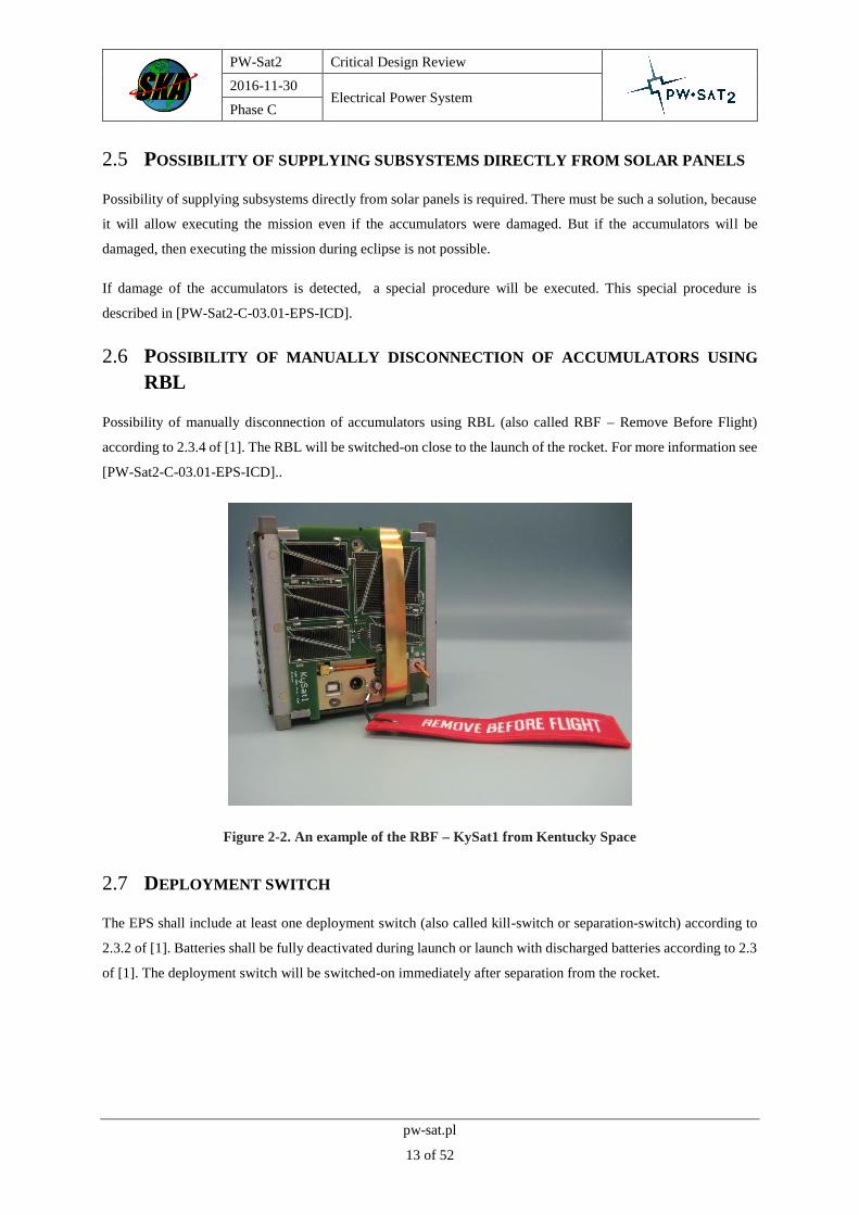
Possibility of manually disconnection of accumulators using RBL (also called RBF – Remove Before Flight)
according to 2.3.4 of [1]. The RBL will be switched-on close to the launch of the rocket. For more information see
[PW-Sat2-C-03.01-EPS-ICD]..
Figure 2-2. An example of the RBF – KySat1 from Kentucky Space
2.7 DEPLOYMENT SWITCH
The EPS shall include at least one deployment switch (also called kill-switch or separation-switch) according to
2.3.2 of [1]. Batteries shall be fully deactivated during launch or launch with discharged batteries according to 2.3
of [1]. The deployment switch will be switched-on immediately after separation from the rocket.

PW-Sat2 Critical Design Review
2016-11-30 Electrical Power System
Phase C
pw-sat.pl
14 of 52
Figure 2-3. Placement for deployment switches – source [1]
We will use two deployment switches for redundancy. The switches will be placed on rails of the PW-Sat2 satellite.
An example of the deployment switch:
Figure 2-4. Deployment switch - surce TISAT-1
2.8 TWO CONTROLLERS FOR REDUNDANCY
The EPS shall contain two redundant controllers. Each one can perform the main purpose of our mission: to open
SAIL. If one of them is broken (any kind of failure), the mission cannot be compromised.

PW-Sat2 Critical Design Review
2016-11-30 Electrical Power System
Phase C
pw-sat.pl
15 of 52
2.9 LCL FOR EACH SUBSYSTEM
Possibility of supply disconnection for every subsystem will allow saving more energy. Keys (electronic switches)
turning on supply voltage shall be located on buses 3.3, 5V and 6.5-9V. Every one of them shall have over-current
protection (also named LCL – Latch-Up Current Limiter) and has to be controlled from OBC. Communication
module COMM and OBC may be disconnected only when an emergency situation appears, so they have to have
their own hardware protection.
2.10 CREATING VOLTAGES 3.3V, 5V AND ACC
Creating voltages 3.3V, 5V and possibility for supplying directly from accumulator package (ACC line). All the
power lines shall be protected by an LCL.
2.10.1 REQUIRED VOLTAGES FOR EACH SUBSYSTEM
Required voltages for each subsystem are listed below:
No. Abbreviation Full name Switches
1 COMM ISIS UHF downlink / VHF uplink Full Duplex
Transceiver Permanent VBAT
2 ANT Deployable UHF and VHF antennas from ISIS
company 5V
3 BATTERY Accumulator package - NanoPower BP4 from
GOMSpace company
Permanent VBAT (for heaters
supply)
4 EPS Electrical Power System Internal
5 ADCS
Attitude Determination and Control System -
ISIS Magnetorquer Board (iMTQ)
Actuators: Permanent 5 V
Sensors and electronics:
Permanent 3.3V
6 PLD Payload electronics
SunS: 1x 3.3V
CamWing: 3.3V
CamNadir: 3.3V
Sensors: 1x 5V
Sail: 2x VBAT (redundancy)
SADS: 2x VBAT (redundancy)

PW-Sat2 Critical Design Review
2016-11-30 Electrical Power System
Phase C
pw-sat.pl
16 of 52
7 OBC On-board Computer Permanent 3.3V
Table 2-1. Required voltages for each subsystem
For more information please see an ICD document for corresponding subsystem.
2.11 EMERGENCY DISCONNECTION WHEN LOW BATTERY
Emergency disconnection of subsystems from accumulators when deep discharge. The module should warn OBC
before disconnecting in order to allow saving latest work results.
2.12 RUNNING IN SPACE ENVIRONMENT
Running in space environment:
vacuum (no convection – problems with cooling). To prevent overheating of the EPS, parameters of
components shall be derated in conformance with [2] standard and all heat dissipative spots shall be agreed
by the TCS team.
high temperature tolerance (-40 to at least 60°C),
known tolerance for cumulative dose radiation,
tolerance for damage of single integrated circuit by radiation or by ESD,
tolerance for ambient plasma (in conformance with B.2 in [3]). We predict that the PW-Sat2 satellite will be
launched on LEO orbit with inclination of around 98° (Sun-synchronous orbit). Dielectric surface can be
charged and some electrostatic discharge can occur. All conductors shall be grounded on the whole spacecraft
(for example conductive layers of the MLI). Floating insulators shall not be used on spacecraft surface -
insulators shall be coated with conductive coating and shall be grounded.
To protect from latch-up damage due to radiation the LCL protections are necessary. Main integrated circuits
should to have radiation tests performed by NASA, ESA, TRAD, JAXA, IEEE or another well-known authority.
2.13 CURRENTS AND VOLTAGES MONITORING
Monitoring of currents and voltages of supply buses, accumulators and solar panels power, temperature
measurements, etc.

PW-Sat2 Critical Design Review
2016-11-30 Electrical Power System
Phase C
pw-sat.pl
17 of 52
2.14 REQUIREMENTS FOR THE PCB
PCB of the EPS shall be designed in compliance with the mechanical PC-104 standard. This is a stackable family
of embedded systems which define mechanical dimensions and electrical interfaces. The electrical interfaces of
the PC-104 standard are not applicable for the PW-Sat2 mission. We will use a well-known electrical interface
specification for CubeSats which are used both by the GOMSpace company, the ISIS company and the ClydeSpace
company.
2.14.1 DIMENSIONS OF THE PCB
Mechanical dimension of the PCB is shown below (drawings [4] from Pumpkin company):
Figure 2-5. Top and side view of the PCB
PC-104 8-bit Bus is not applicable (holes are not drilled) for the PW-Sat2 mission.
PW-Sat2 Critical Design Review
2016-11-30 Electrical Power System
Phase C
pw-sat.pl
18 of 52
Figure 2-6. Bottom view of the PCB
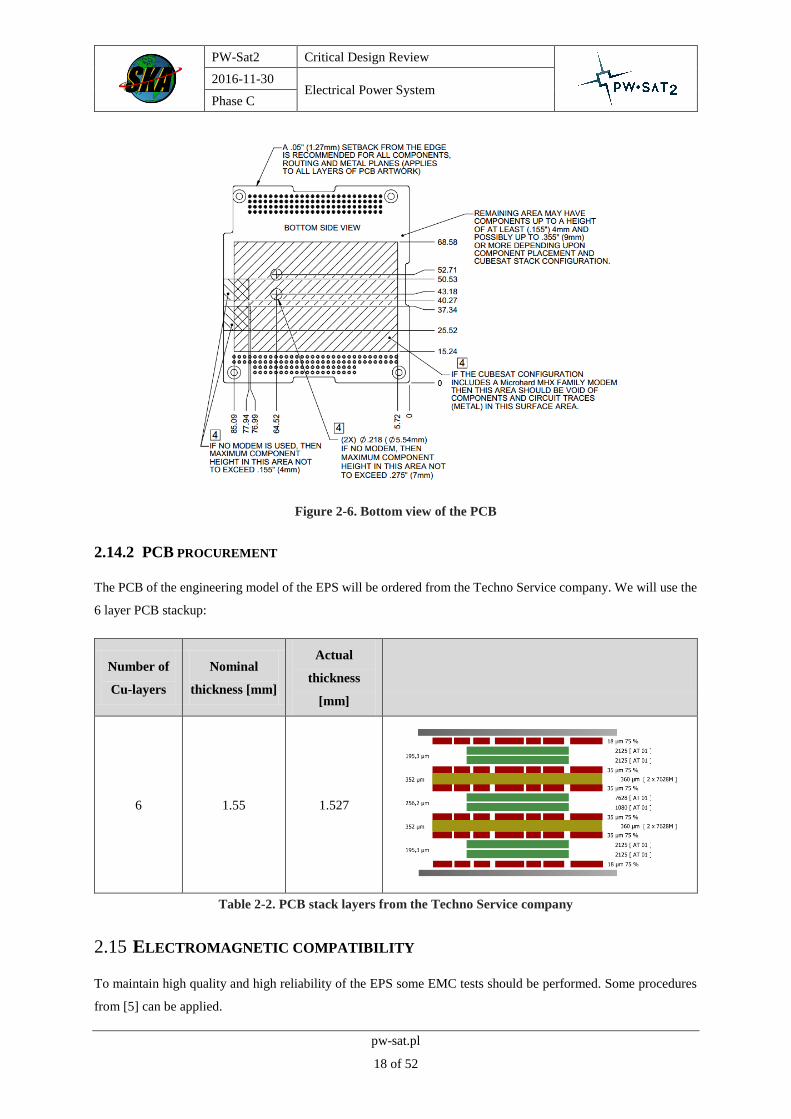
2.14.2 PCB PROCUREMENT
The PCB of the engineering model of the EPS will be ordered from the Techno Service company. We will use the
6 layer PCB stackup:
Number of
Cu-layers
Nominal
thickness [mm]
Actual
thickness
[mm]
6 1.55 1.527
Table 2-2. PCB stack layers from the Techno Service company
2.15 ELECTROMAGNETIC COMPATIBILITY
To maintain high quality and high reliability of the EPS some EMC tests should be performed. Some procedures
from [5] can be applied.

PW-Sat2 Critical Design Review
2016-11-30 Electrical Power System
Phase C
pw-sat.pl
19 of 52
3 EPS DESIGN
A simplified block diagram shows the main idea of the electrical power system:
Kill-Switch RBLMPPT X
MPPT Y+
MPPT Y-
Controller B
Controller A
Battery Controller
Battery Pack NC NO
3V3 DCDC converter
LCLs for
DCDCs5V DCDC converter
5V
3V3
Distribution
Solar panels X+ and X-
Solar panel Y+
RBL switch
Internal supply
PC-104 stack connector
VBAT
Solar panel Y-
EXT
X
EXT
Y+
EXT
Y-
I2C
BU
S
I2C
PLD
Sub
syst
ems
To ANTenna module
Figure 3-1 Simplified block diagram
3.1 MPPT REGULATORS
MPPT regulators are responsible for converting electrical power which is harvested by solar panels. A single
MPPT regulator consists of controlled DCDC converter, current and voltage measurement circuits, ADC and DAC
converters which are controlled with controller A or B (depends on channel). Solar panels are connected to X+,
X-, Y+ and Y- inputs.

PW-Sat2 Critical Design Review
2016-11-30 Electrical Power System
Phase C
pw-sat.pl
20 of 52
Figure 3-2 Solar panels Y+, Y- and X+ - source [PW-Sat2-C-10.00-CONF-CDR]
Figure 3-3 Solar panels X- - source [PW-Sat2-C-10.00-CONF-CDR]
Y+ solar panel
Y- solar panel
X+ solar panel
X- solar panel

PW-Sat2 Critical Design Review
2016-11-30 Electrical Power System
Phase C
pw-sat.pl
21 of 52
In addition, the MPPT regulators may convert electrical power which is provided from EGSE through EXT X,
EXT Y+ and EXT Y- inputs. This feature allows to charge the batteries and test the EPS before launch.
Detailed diagram of the MPPT regulators:
Solar panel X+
Solar panel X-
EXT XEMI
FiltersI and V
MeasurementsControlled DCDC
converterTo MPB
EXT Y+
Solar panel Y+
EMI Filters
I and V Measurements
Controlled DCDC converter
EMI Filters
I and V Measurements
Controlled DCDC converter
EXT Y-
Solar panel Y-
Figure 3-4 MPPT regulators
The controller A is responsible for controlling the MPPT X and MPPT Y+ regulators. The controller B controls
the MPPT Y- regulator.
3.1.1 ORING DIODES FOR SOLAR PANELS
Four solar panels are connected to three MPPT regulators. Because of X+ and X- solar panels are on the opposite
sides they are ORed to a single MPPT regulator. The Y+ and Y- solar panels have two independent MPPT
regulators.
Figure 3-5 Oring diodes and EMI filters for solar panels X+ and X-

PW-Sat2 Critical Design Review
2016-11-30 Electrical Power System
Phase C
pw-sat.pl
22 of 52
Figure 3-6 Oring diodes and EMI filters for solar panels Y+ and Y-
3.1.2 INPUT EMI FILTERS
To decrease EMI susceptibility of the system, the additional input EMI filters were applied. Both differential mode
and common mode filters for solar panels were applied. For EXT supply lines just differential mode filters were
applied (in EGSE additional common mode filters should be applied).
Figure 3-7 EMI filters for solar panels X+ and X-

PW-Sat2 Critical Design Review
2016-11-30 Electrical Power System
Phase C
pw-sat.pl
23 of 52
Figure 3-8 EMI filters for solar panels Y+ and Y-
3.1.3 I AND V MEASUREMENTS
To perform MPPT regulation, the MPPT regulator measures input voltage and current. These values are available
in telemetry.
I and V measurements are realised with the same circuits for all MPPT regulators:
Figure 3-9 MPPT measurements
3.1.4 CONTROLLED DCDC CONVERTER
This unit contains: a controlled DCDC converter with input and output filters. The MPPT X contains a boost
converter, the MPPT Y+ and Y- contain buck-boost converters.
A controlled boost converter for MPPT X:

PW-Sat2 Critical Design Review
2016-11-30 Electrical Power System
Phase C
pw-sat.pl
24 of 52
Figure 3-10 Boost converter for MPPT X
3.1.5 ORING DIODES TO MPB
There are three ORing diodes, a single diode for a single MPPT regulator. These diodes are responsible for
summing MPPT regulators to MPB bus.
Figure 3-11 ORing diodes to MPB
3.2 BATTERY CONTROLLER
This is a power stage for the battery controller feature. Both Controller A and B are responsible for controlling the
power stage. Appropriate algorithms maintain the batteries in the suitable conditions.

PW-Sat2 Critical Design Review
2016-11-30 Electrical Power System
Phase C
pw-sat.pl
25 of 52
Figure 3-12 Power stage for battery controller
3.3 KILL-SWITCH CIRCUIT
The kill-switch circuit ensures that the whole system is not active during launch. This circuit consists of two
external electro-mechanical switches which are responsible to cut-off subsystems from both battery pack and solar
panels.
Figure 3-13. Placement for deployment switches – source [PW-Sat2-C-10.00-CONF-CDR]
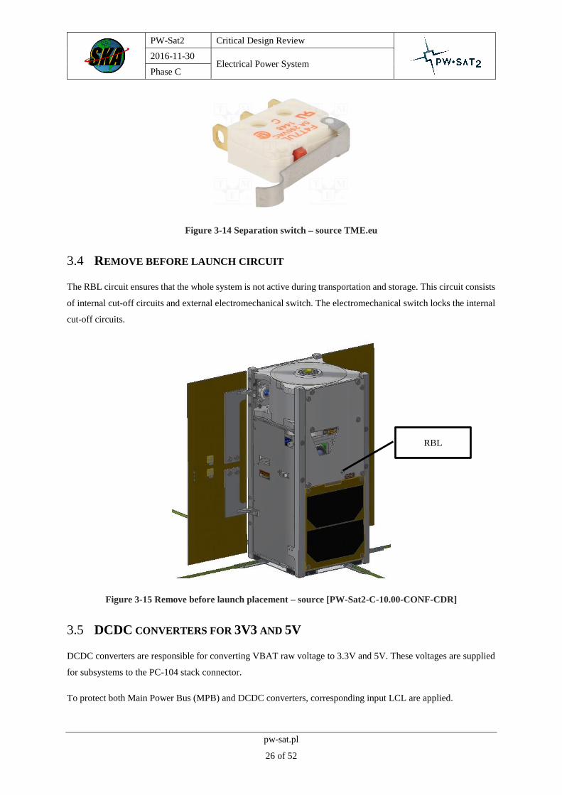
There are two F4T7YCUL switched on the Z- side. The F4T7YCUL is shown below:
PW-Sat2 Critical Design Review
2016-11-30 Electrical Power System
Phase C
pw-sat.pl
26 of 52
Figure 3-14 Separation switch – source TME.eu
3.4 REMOVE BEFORE LAUNCH CIRCUIT
The RBL circuit ensures that the whole system is not active during transportation and storage. This circuit consists
of internal cut-off circuits and external electromechanical switch. The electromechanical switch locks the internal
cut-off circuits.
Figure 3-15 Remove before launch placement – source [PW-Sat2-C-10.00-CONF-CDR]
3.5 DCDC CONVERTERS FOR 3V3 AND 5V
DCDC converters are responsible for converting VBAT raw voltage to 3.3V and 5V. These voltages are supplied
for subsystems to the PC-104 stack connector.
To protect both Main Power Bus (MPB) and DCDC converters, corresponding input LCL are applied.
RBL

PW-Sat2 Critical Design Review
2016-11-30 Electrical Power System
Phase C
pw-sat.pl
27 of 52
Figure 3-16 3V3 and 5V DCDC converters for subsystems
3V3 and 5V DCDC converters consist of a buck converter with input and output EMI filters:
Figure 3-17 Input and output filters for 3V3 and 5V DCDC converters
A DCDC converter for 3V3 line:

PW-Sat2 Critical Design Review
2016-11-30 Electrical Power System
Phase C
pw-sat.pl
28 of 52
Figure 3-18 3V3 DCDC converter
3.6 INTERNAL SUPPLY
This part provides supply voltages to internal EPS’ circuits. Internal supply should be as reliable as possible. In
our design we implemented two separated supply stages for two controllers:
Figure 3-19 Internal supply
Detailed schematic diagram of a single supply circuit:

PW-Sat2 Critical Design Review
2016-11-30 Electrical Power System
Phase C
pw-sat.pl
29 of 52
Figure 3-20 A single internal supply circuit
Apart from LDO regulators, it contains a hardware watchdog. It is responsible for performing a power cycle for
selected controller when any malfunction occurred.
3.7 CONTROLLERS
There are two independent controllers in the EPS. To increase reliability of the system, they are completely
separated from point of view of electrical connections.
3.7.1 CONTROLLER A
The controller A is responsible for controlling most of the features of the EPS.
As the controller A we will use the ATMega325PV from Atmel corp.

PW-Sat2 Critical Design Review
2016-11-30 Electrical Power System
Phase C
pw-sat.pl
30 of 52
Figure 3-21 ATMega325 [6] - Controller A
3.7.2 CONTROLLER B
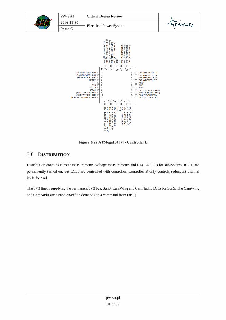
Controller B controls redundant thermal knife for Sail and it is responsible for voting with Controller A for critical
features.
As the controller B we will use the ATMega164PV from Atmel corp.
PW-Sat2 Critical Design Review
2016-11-30 Electrical Power System
Phase C
pw-sat.pl
31 of 52
Figure 3-22 ATMega164 [7] - Controller B
3.8 DISTRIBUTION
Distribution contains current measurements, voltage measurements and RLCLs/LCLs for subsystems. RLCL are
permanently turned-on, but LCLs are controlled with controller. Controller B only controls redundant thermal
knife for Sail.
The 3V3 line is supplying the permanent 3V3 bus, SunS, CamWing and CamNadir. LCLs for SunS. The CamWing
and CamNadir are turned on/off on demand (on a command from OBC).

PW-Sat2 Critical Design Review
2016-11-30 Electrical Power System
Phase C
pw-sat.pl
32 of 52
3V3
LCL
LCL
LCL
Permanent 3V3 bus
SunS 3V3
CAMwing 3V3
CAMnadir 3V3
I and V measurement
RLCL
Figure 3-23 Distribution for 3V3 lines
The 5V line is supplying the permanent 5V bus, ANTenna module and SENS line (which supplies all sensors on
PLD board). Both ANTenna module and SENS line are turned on/off on demand (on a command from OBC).
5V
LCL
LCL
Permanent 5V bus
ANTenna 5V
SENS 5V (PLD board)
I and V measurement
RLCL
Figure 3-24 Distribution for 5V lines
The VBAT line is connected through a RLCL to the PC-104 stack connector as the permanent VBAT bus. The
VBAT bus provides supply voltages to deployment LCLs and switches also.
Permanent VBAT bus
SAIL main thermal knifeLCL
Switch
Switch
LCLSwitch
Switch
SADS main thermal knife
SAIL red. thermal knife
SADS red. thermal knife
RLCLI and V
measurementVBAT
Figure 3-25 Distribution for VBAT lines
Detailed block diagram of the distribution unit:

PW-Sat2 Critical Design Review
2016-11-30 Electrical Power System
Phase C
pw-sat.pl
33 of 52
Figure 3-26 Distribution detailed block diagram

PW-Sat2 Critical Design Review
2016-11-30 Electrical Power System
Phase C
pw-sat.pl
34 of 52
4 COMPONENTS SELECTION
4.1 MICROCONTROLLER SELECTION
In EPS microcontroller(s) will be responsible for MPPT (to control boost and buck-boost converters) and doing
measurements of current/voltages in each channel – basic telemetry.
4.1.1 REQUIREMENTS
Requirements:
due to it is low usage (basic calculations does not take much processor time) it should allow for under-clocking
for lower power consumption,
low starting voltage (preferably 1.8V),
I2C (slave) interface for communicating with OBC,
radiation-tests and examples in space,
extended temperature range,
low complexity – also connected with transistor technological process,
well-known architecture and known bugs/problems,
flash memory about 16kB,
JTAG interface for debugging and programming,
Bootloader and ISP programming for on-board reprogram
It was chosen to use ATMega family from Atmel corporation.
4.1.2 PART SELECTION
4.1.2.1 ATMega parts codes
An example:
ATMEGA164PV-10AQR
Table 4-1. An example of ATMega part code
164 – part number
Before hyphen:
P –pico-power - some improvements to core and ability to put controller in deeper sleep mode,
V – lower starting voltage (1.8V), lower clock (10 MHz maximum),
A – new production line (possibility of smaller transistor process due to reduction of power consumption).

PW-Sat2 Critical Design Review
2016-11-30 Electrical Power System
Phase C
pw-sat.pl
35 of 52
After hyphen:
"10" - maximum clock frequency (in MHz),
A/M/P - package (A - TQFP; M - MLF; P - PDIP),
Q/U - temperature range (Q - up to 105 degrees Celsius, U - normal),
R - tape & reel.
4.1.2.2 Preferred part code:
V – low starting voltage,
P – pico-power model,
10MHz clock,
A package (TQFP model),
Q temperature range (extended).
4.1.2.3 Couple microcontrollers to review
Couple microcontrollers to review were selected and they are shown below:
4.1.2.3.1 ATMEGA164P-B15AZ – automotive series
Automotive series of ATMega164 microcontroller.
Inconsistency with operating voltage – on Atmel website 1.8V, in datasheet 2.7V.
Pros Cons
Extended (-40 to 125 degrees) temperature range Operation voltage from 2.7V
Table 4-2. ATMEGA164P-B15AZ – automotive series
4.1.2.3.2 ATMega16(L)
Oldest microcontroller from Atmel with 16kB of flash memory.
Pros Cons
probably low technological process in old
production line
Starting voltage from 2.7V
old core with some registers with strange access
(ex. URSEL bit in UCSRC register)
Table 4-3. ATMega16 review
4.1.2.3.3 ATMega164
Pros Cons
Starting voltage from 1.8V
PW-Sat2 Critical Design Review
2016-11-30 Electrical Power System
Phase C
pw-sat.pl
36 of 52
New core with better access
2x SPI, 2xI2C interfaces
Table 4-4. ATMega164 review
4.1.2.3.4 ATMega168
Pros Cons
Starting voltage from 1.8V No JTAG interface
New core with better access to registers
2x SPI, 2xI2C interfaces
Table 4-5. ATMega168 review
4.1.2.4 Selected part
For flight model ATMEGA164PV-10AQ was selected.
It is available from Digikey distributor.
For engineering model ATMEGA164PV-10AU was selected. The only difference is the temperature range. This
part is wider available.
4.1.3 RADIATION EFFECT ANALYSIS IN ATMEGA
Analysis is based on radiation tests made by CERN (ATMega128) [8] and IEEE (ATMega128) [9]. Both
processors are similar to chosen one, but with larger flash memory. Technological process should be similar.
CERN has made numerous tests it’s ELMB (Embedded Local Monitor Board) – also for older version with
ATMega103 (actually obsolete). Technological processes are noted as follows: 103L – 500nm; 128 – 350nm.
Despite that, it was shown that newer processors behave better and are more immune to radiation effects.
It is considered that chosen microprocessor has technological process of 350nm also.
4.1.3.1 Total Ionising Dose (TID)
IEEE made TID tests with dose rate up to 17.1 rad/s – ATMega1280 was fully operational up to 18.3kRad. There
was no significant current changes. “The initial failure was detected in the ADC test at 27.3kRad (Si) followed by
complete loss of functionality at 28.3kRad (Si).”
Test conducted by CERN shown similar results – after radiation to 18 - 25krad devices were fully operational (3
months after radiation, it was not able to test them earlier – but [9] shown that there were not recovery with time).
Only encountered problem was reFlashing device – “About 100 of 30000 flash memory addresses failed to
program correctly.”.

PW-Sat2 Critical Design Review
2016-11-30 Electrical Power System
Phase C
pw-sat.pl
37 of 52
4.1.3.2 Single event effects (SEE)
4.1.3.2.1 Latch-ups
Due to possible latch-ups the microcontroller will be protected with a current-limiter and reset device. Some events
are recovered automatically some require reset of processor and other are recovered after power cycling.
4.1.3.2.2 Flash memory
SEU in flash memory will lead to bit change – and corruption of program data.
Tests in [8] have not detected errors with flash memory – with proton fluency of 1.3 ⋅ 1012 𝑝𝑟𝑜𝑡𝑜𝑛𝑠/𝑐𝑚^2 there
were no flash memory errors.
Due to possibility of reprogramming device in-flight and to provide ability to restore original software (in case
error is detected in memory) there will be a bootloader. More detailed information is in corresponding section.
4.1.3.3 EEPROM memory
Similar to flash, there was no detected errors in EEPROM memory. Despite that, it was chosen to use external
FRAM memory due to its immunity for TID.
4.1.3.4 SRAM memory
SEE in SRAM memory was tested in [8].
Most SEE in this IC are bit changes in SRAM memory. This can lead to problems with numerical calculus and
even bad controlling MPPT. There will be both hard- and software protection for these kind of effects.

PW-Sat2 Critical Design Review
2016-11-30 Electrical Power System
Phase C
pw-sat.pl
38 of 52
Figure 4-1. SEE in 2048 bytes of SRAM – source [8]
There is a very big difference within technology change – newer processors produce less errors than older ones.
4.1.3.5 Other memories
Registers and other memories (ADC, CAN configuration, etc.) has shown little amount of errors – which can lead
to changing configuration of given peripheral.
4.1.4 ATMEGA SELECTION CONCLUSION
Numerous ATMega microcontrollers tests were held. CERN researches shown ATMega128 immunity is sufficient
for PW-Sat2. Our selected processor is very similar (but it has less flash memory size – so the SEE in flash is
reduced).
TID tests shown that ATMega is immune to expected radiation dose.
Considering SEE ATMega main problem can be bit squatting in SRAM memory – but it can be protected from it
via multiple calculations, redundancy etc.
4.1.5 PROGRAMMING ATMEGA MICROCONTROLLER
4.1.5.1 Bootloader
For changing flash memory content (firmware) when in orbit it was proposed to use bootloader connected to
FRAM memory.

PW-Sat2 Critical Design Review
2016-11-30 Electrical Power System
Phase C
pw-sat.pl
39 of 52
Firmware from ground, passing to EPS microcontrollers (via I2C satellite bus) will be stored in FRAM memory –
and after reset microcontroller will re-program itself. Holding data in FRAM memory will provide redundancy to
flash memory – when the error is detected in firmware (via ex. CRC) microcontroller will automatically upload
firmware from FRAM memory.
4.1.5.2 In-System Programming interface
Due to possibility of error in bootloader section of flash memory it should be possible to program the bootloader
from other source. One of possibilities is use of ATMega ISP protocol. It is simple SPI protocol which can be used
to upload new firmware to Flash/EEPROM memories inside microcontroller. Possible solution is to connect two
EPS microcontrollers via SPI bus. Problem encountered – they have to have RESET connected to each other –
when one fails, it can hold second one in RESET state.
4.1.5.3 JTAG protocol
On ground, when developing software for EPS the JTAG programmer/debugger will be used. It can be used for
step execution, variables watches, breakpoints etc. In flight model, firmware upload method used will be
bootloader. It is not considered as option for in-flight firmware upload due to its complex protocol, number of I/O
needed and no further advantages.
PW-Sat2 Critical Design Review
2016-11-30 Electrical Power System
Phase C
pw-sat.pl
40 of 52
5 CURRENT STATE OF WORK
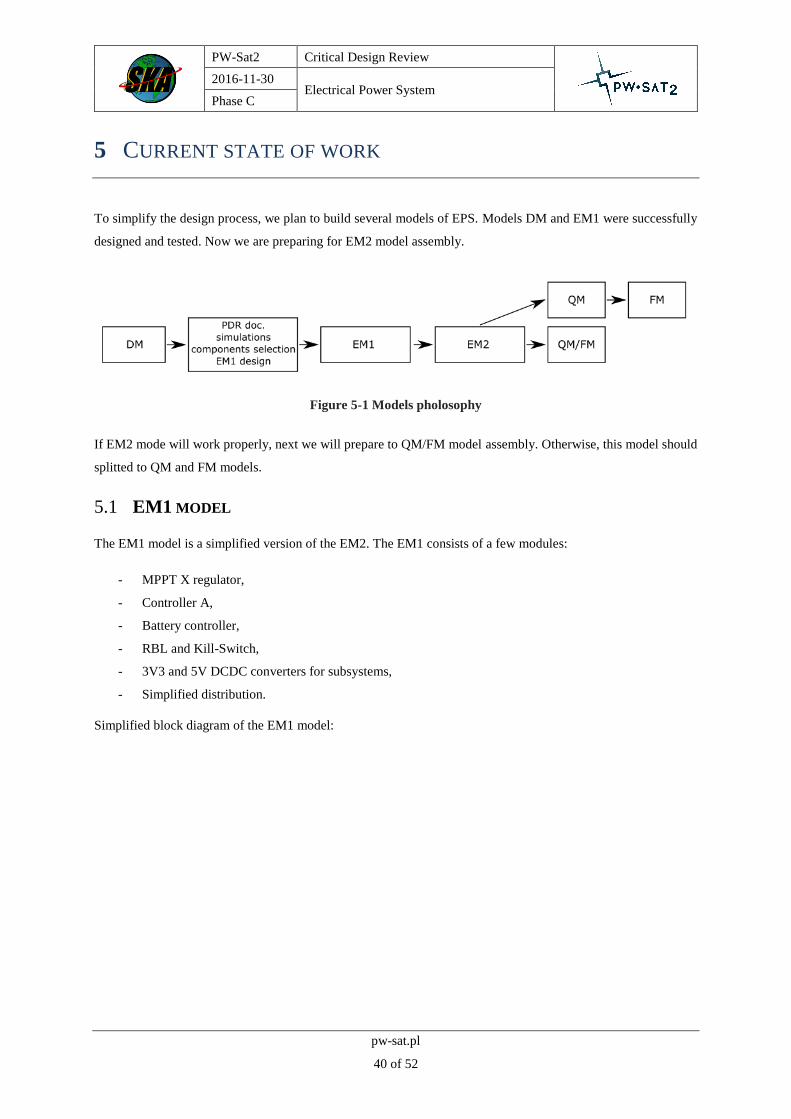
To simplify the design process, we plan to build several models of EPS. Models DM and EM1 were successfully
designed and tested. Now we are preparing for EM2 model assembly.
Figure 5-1 Models pholosophy
If EM2 mode will work properly, next we will prepare to QM/FM model assembly. Otherwise, this model should
splitted to QM and FM models.
5.1 EM1 MODEL
The EM1 model is a simplified version of the EM2. The EM1 consists of a few modules:
- MPPT X regulator,
- Controller A,
- Battery controller,
- RBL and Kill-Switch,
- 3V3 and 5V DCDC converters for subsystems,
- Simplified distribution.
Simplified block diagram of the EM1 model:

PW-Sat2 Critical Design Review
2016-11-30 Electrical Power System
Phase C
pw-sat.pl
41 of 52
Figure 5-2 Simplified block diagram of the EM1 model
5.1.1 EM1 SUB-MODULES
The EM1 had been developed as evaluation board version in order to verify electronics design. Every sub-module
was manufactured as a separated PCB. Some of these modules were listed below.
MPPT X regulated boost converter which was controlled with controller A:
Figure 5-3 EM1 model - boost converter for MPPT X
Ideal diode which was used for solar panels ORing and MPPT to MPB ORing:

PW-Sat2 Critical Design Review
2016-11-30 Electrical Power System
Phase C
pw-sat.pl
42 of 52
Figure 5-4 EM1 model - Ideal diode for solar panels and MPB ORing
RBL and Kill-Switches interface:
Figure 5-5 EM1 - RBL and Kill-Switches
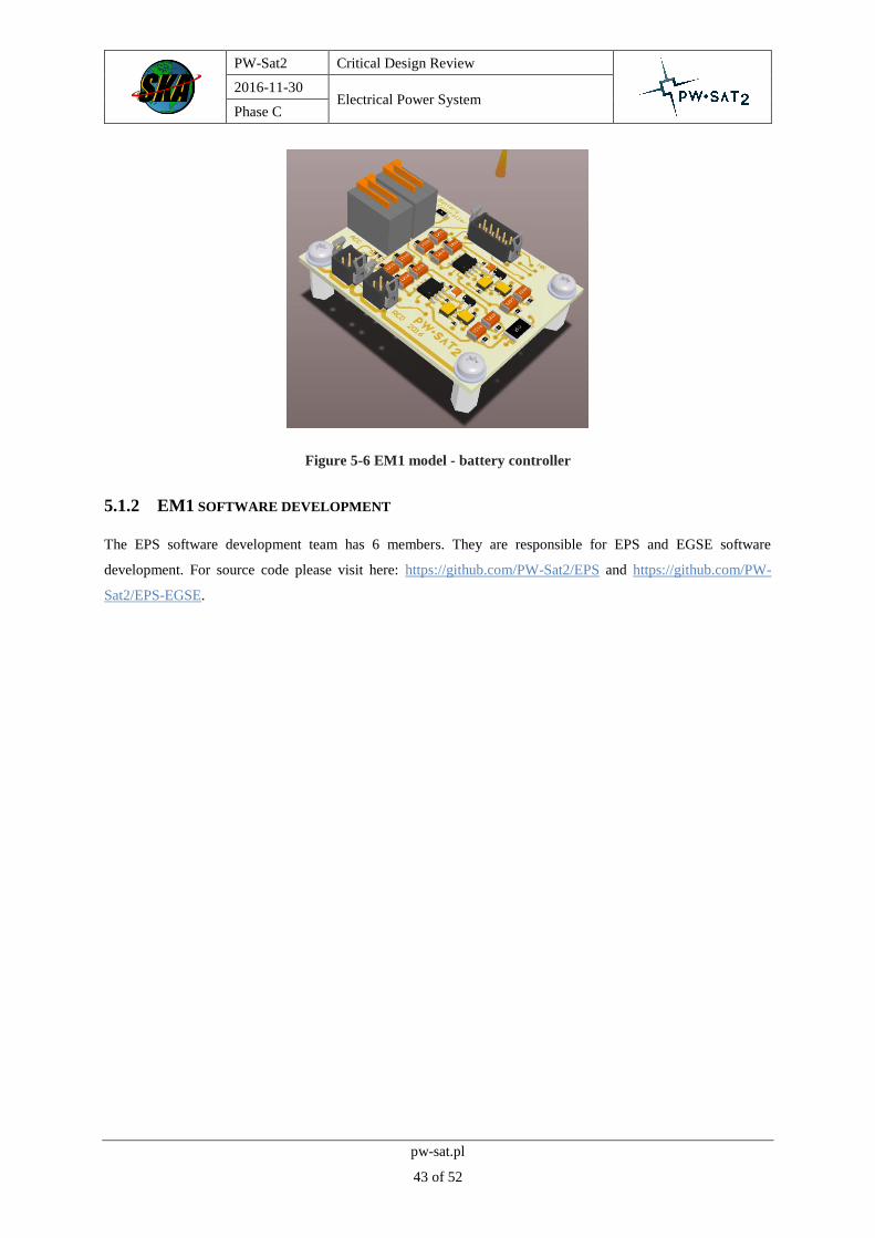
A power stage for battery controller:
PW-Sat2 Critical Design Review
2016-11-30 Electrical Power System
Phase C
pw-sat.pl
43 of 52
Figure 5-6 EM1 model - battery controller
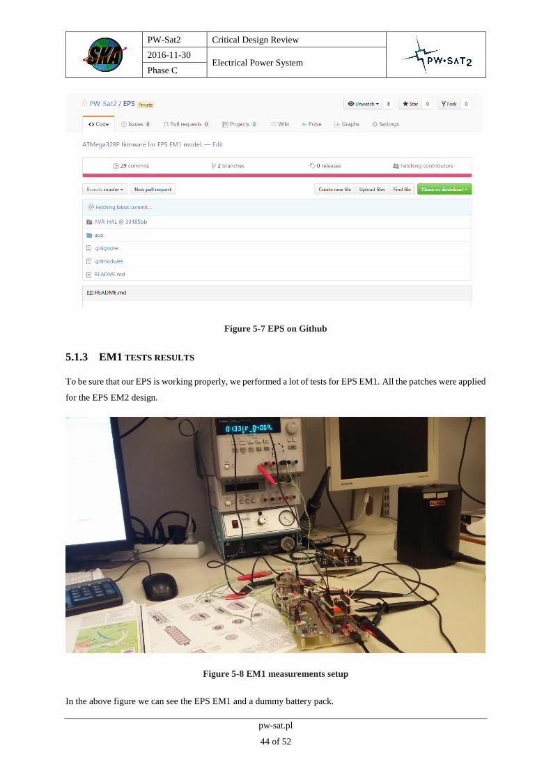
5.1.2 EM1 SOFTWARE DEVELOPMENT
The EPS software development team has 6 members. They are responsible for EPS and EGSE software
development. For source code please visit here: https://github.com/PW-Sat2/EPS and https://github.com/PW-
Sat2/EPS-EGSE.
PW-Sat2 Critical Design Review
2016-11-30 Electrical Power System
Phase C
pw-sat.pl
44 of 52
Figure 5-7 EPS on Github
5.1.3 EM1 TESTS RESULTS
To be sure that our EPS is working properly, we performed a lot of tests for EPS EM1. All the patches were applied
for the EPS EM2 design.
Figure 5-8 EM1 measurements setup
In the above figure we can see the EPS EM1 and a dummy battery pack.

PW-Sat2 Critical Design Review
2016-11-30 Electrical Power System
Phase C
pw-sat.pl
45 of 52
5.1.3.1 Battery pack deep discharge
This test shows that the EPS is able to disconnect subsystems from battery pack when battery is low. The EPS
should cut-off subsystems when voltage is low (battery pack voltage is lower than 6.5V). The graph shows this
behaviour:
Figure 5-9 Battery pack deep discharge
The simulated OBC was disconnected from supply and it stops sending telemetry.
5.1.3.2 Battery charging and discharging cycles
Battery charging and discharging cycles were shown below:

PW-Sat2 Critical Design Review
2016-11-30 Electrical Power System
Phase C
pw-sat.pl
46 of 52
Figure 5-10 EM1 battery pack charging/discharging cycles
5.1.3.3 MPPT X regulator performance
The MPPT X regulator was examined from point of view of performance. We simulated sunlight witch an external
solar panels simulator:
Power supply (CC mode)Iout = 0.5AVout = 5.5V
0.5Ω
PGND
EXT X
6x1N4007
Figure 5-11 Solar panels simulator for MPPT X
Other MPPT regulators were simulated with remote controlled power supplies. MPPT X regulator performance:

PW-Sat2 Critical Design Review
2016-11-30 Electrical Power System
Phase C
pw-sat.pl
47 of 52
Figure 5-12 EM1 - MPPT X performance
Sunlight was changed periodically.
We performed stability measurements for the MPPT DCDC regulated converter. The measurement setup:

PW-Sat2 Critical Design Review
2016-11-30 Electrical Power System
Phase C
pw-sat.pl
48 of 52
Figure 5-13 EM1 stability measurements
We used the Ridley AP300 FRA. Bode plot of the DCDC converter:
Figure 5-14 EM1 MPPTX bode plot
This chart confirms that the MPPTX regulator meets these requirements. The phase margin is equal to 60° and the
magnitude margin is higher than 14dB.
5.2 EM2 MODEL
The EM2 model was designed and we are preparing for assembling. The electrical design was described
previously. For mechanical drawings and detailed electrical characteristics please see [PW-Sat2-C-03.01-EPS-
ICD].

PW-Sat2 Critical Design Review
2016-11-30 Electrical Power System
Phase C
pw-sat.pl
49 of 52
6 TESTS PLAN FOR EM2
6.1 KILL-SWITCHES
To be sure that the Kill-Switch mechanism is working properly, a special test should be performed.
Figure 6-1 Kill-Swtches test
When the Kill-Switch deactivates EPS, a voltage after the Kill-Switch should be close to 0V.
6.2 EMC - RADIATION SUSCEPTIBILITY
The COMM module radiates very high RF power. The EPS should work properly in harsh RF environment. A
proper test is planned:

PW-Sat2 Critical Design Review
2016-11-30 Electrical Power System
Phase C
pw-sat.pl
50 of 52
Figure 6-2 EMC - radiation susceptibility
6.3 EMC – CONDUCTED EMISSION
Conducted emission on supply lines should be measured. Measurement procedures and limits will be applied
according to [5].
Figure 6-3 EMC - conducted emission @ inputs

PW-Sat2 Critical Design Review
2016-11-30 Electrical Power System
Phase C
pw-sat.pl
51 of 52
Figure 6-4 EMC - conducted emission @ outputs
6.4 EMC – PHASE MARGINS FOR DCDC CONVERTERS
We decided to test all DCDC converters from point of view of stability. We selected 60° phase margin and 10dB
magnitude margin. All DCDC converters should meet these requirements.
Figure 6-5 DCDC stability measurements

PW-Sat2 Critical Design Review
2016-11-30 Electrical Power System
Phase C
pw-sat.pl
52 of 52
7 EPS EGSE
To examine the EPS performance, a special EGSE was designed. The EGSE can simulate subsystems from point
of view of loads. The EGSE was designed and fully assembled and it is ready to use.
Figure 7-1 EPS EGSE
The EGSE board can be used both for EM2 and for next models.


