Page 1
ELECTRICAL PROPERTIES OF ZnO GROWN BY
METALORGANIC VAPOUR PHASE EPITAXY
by
Dichen Li B.Sc., University of Science and Technology of China, 2008
THESIS SUBMITTED IN PARTIAL FULFILLMENT OF THE REQUIREMENTS FOR THE DEGREE OF
MASTER OF SCIENCE
In the Department of Physics
© Dichen Li 2011
SIMON FRASER UNIVERSITY
Summer 2011
All rights reserved. However, in accordance with the Copyright Act of Canada, this work may be reproduced, without authorization, under the conditions for Fair Dealing. Therefore, limited reproduction of this work for the purposes of private
study, research, criticism, review and news reporting is likely to be in accordance with the law, particularly if cited appropriately.
Page 2
ii
APPROVAL
Name: Dichen Li
Degree: Master of Science
Title of Thesis: Electrical Properties of ZnO Grown by Metalorganic Vapour Phase Epitaxy
Examining Committee:
Chair: Dr. J. Steven Dodge
______________________________________
Supervisor Dr. Simon Watkins
______________________________________
Supervisor Dr. Karen Kavanagh
______________________________________
Supervisor Dr. Patricia Mooney
______________________________________
Internal Examiner Dr. Gary Leach
Date Defended/Approved: ______________________________________
Page 3
iii
ABSTRACT
ZnO is a wide band gap semiconductor which is a good candidate for the next generation
of visible and ultraviolet optoelectronic devices. The electrical properties of thin film
ZnO grown on sapphire by metalorganic vapour phase epitaxy (MOVPE) were
investigated in this thesis. Hall measurements were performed to determine the electrical
properties of the ZnO layers. Films were found to be n-type in all cases with residual
carrier densities in the range 5×10¹⁷
to 2×10¹⁸
cm-3
. The addition of In dopant did not
result in a significant increase in n-doping despite a large In concentration determined by
secondary ion mass spectrometry and low temperature photoluminescence spectroscopy.
Temperature dependent Hall measurements showed carrier freeze-out with an activation
energy of ~30 meV which is attributed to native donors. No significant change in
activation energy was observed for In doping, consistent with poor activation of the In
impurities. These data indicate that under the present conditions, In primarily
incorporates as an electrically inactive phase. Thermally deposited Al Ohmic contacts
were developed, having a sheet resistance of <10-5
Ω cm2. Devices were fabricated with
top side Al Ohmic contacts and Au rectifying contacts on ZnO epilayers. The effect of
oxygen plasma and hydrogen peroxide wet treatments were studied by I-V and C-V
measurements. Au-ZnO devices showed rectifying behaviour but with significant leakage
and high ideality factors compared with bulk substrate material. Some improvement was
observed for devices treated with oxygen plasma treatment.
Page 4
iv
ACKNOWLEDGEMENTS
I would like to thank my mother, my grandmother, all my friends and my supervisor
Simon Watkins
Page 5
v
TABLE OF CONTENTS
Approval .......................................................................................................................... ii
Abstract .......................................................................................................................... iii
Acknowledgements ........................................................................................................ iv
Table of Contents ............................................................................................................ v
List of Figures................................................................................................................ vii
List of Tables ................................................................................................................... x
1: Introduction ............................................................................................................... 1
2: Theory ........................................................................................................................ 3
2.1 Metal-semiconductor contact................................................................................... 3
2.1.1 Schottky barrier model of rectifying contacts ................................................ 3 2.1.2 Current-voltage characteristics .................................................................... 7 2.1.3 Capacitance-Voltage characteristics ............................................................ 8 2.1.4 Ohmic contacts .......................................................................................... 10 2.1.5 Transmission line measurements .............................................................. 12
2.2 Hall effect .............................................................................................................. 17
2.2.1 Hall effect theory ........................................................................................ 17 2.2.2 van der Pauw theory .................................................................................. 19 2.2.3 Temperature dependent Hall measurements ............................................. 21
3: Experimental methods ............................................................................................ 25
3.1 Photolithography ................................................................................................... 25
3.1.1 Mask design .............................................................................................. 25
3.2 Procedure for preparation of Hall measurement samples ...................................... 33
4: Material properties .................................................................................................. 35
4.1 Comparison of structural properties of ZnO films on Si and sapphire substrates ............................................................................................................. 35
4.2 Electrical properties ............................................................................................... 40
5: Metal-ZnO junctions ................................................................................................ 56
5.1 Transmission Line Measurements ......................................................................... 57
5.2 Rectifying Au contacts for ZnO on Si substrates.................................................... 61
5.3 Rectifying Au contacts for ZnO on sapphire substrates ......................................... 65
5.3.1 Rectifying Au contacts on as-received samples ......................................... 65 5.3.2 Surface treatment for ZnO/sapphire rectifying contacts ............................. 74
Page 6
vi
6: Conclusions and Future work ................................................................................ 81
Appendix ...................................................................................................................... 83
Summary of growth conditions and Hall measurements for samples processed into Au-ZnO diodes. .............................................................................................. 83
Bibliography ................................................................................................................ 84
Page 7
vii
LIST OF FIGURES
Figure 2.1 Band diagram of metal and semiconductor before contact ....................................... 4
Figure 2.2 Band diagram of metal and semiconductor when contacted to each other ................. 5
Figure 2.3 Schottky diode with energy band diagram (a) under forward bias (b) under
reverse bias. ...................................................................................................... 6
Figure 2.4 (a) Ohmic contact for n type semiconductor before contact; (b) the equilibrium
band diagram for the junction. ........................................................................... 11
Figure 2.5 Schematic diagram showing current flow between metal contacts adapted
from [5] .......................................................................................................... 12
Figure 2.6 Schematic of current flowing from semiconductor into metal contact and
equivalent circuit with the current choosing the path of least resistance
adapted from [5] .............................................................................................. 13
Figure 2.7 Transfer length method (a) diagram of test structure and (b) plot of total
resistance versus contact spacing adapted from [5] .............................................. 16
Figure 2.8 Geometry for measuring Hall effect adapted from [3]. .......................................... 17
.Figure 2.9 Contact for (a) resistivity measurement (b) Hall measurement. .............................. 19
Figure 2.10 The energy band diagram for (a) donor state of non-degenerate and (b)
degenerate n-type semiconductors. .................................................................... 22
Figure 3.1 Schematic of devices for (a) side view (b) top view. ............................................. 26
Figure 3.2 (a) Mask for fabricating rectifying Au contacts. Light areas represent regions
where light passes through. Al mask is similar but with larger circles and the
light and dark areas are reversed. (b) superposition of two masks used to
fabricate TLM samples. Green shows exposed ZnO surface of mesa. Purple
shows Al contact area. ...................................................................................... 27
Figure 3.3 Fabrication procedure for rectifying contact devices. ........................................... 28
Figure 3.4 Optical microscope image of a typical device after processing (H085).
Diameter of the largest Au contacts is 500 µm. .................................................... 31
Figure 3.5 Fabrication procedure for TLM samples. ............................................................ 32
Figure 3.6 Optical micrograph of a typical device for TLM measurement (H075). ................... 33
Figure 4.1 XRD ω scan for the ZnO(002) plane grown on Al2O3(001) and Si(111)
substrates performed by David Huang. ............................................................... 36
Figure 4.2 (101) Pole figure for ZnO on a sapphire substrate. ................................................ 37
Figure 4.3 XRD φ-scan for (a) ZnO/Al2O3 (101) plane scan, (b) Al2O3 substrate (202)
plane scan, (c) ZnO/Si (101) plane scan performed by David Huang. ..................... 38
Page 8
viii
Figure 4.4 Selective area electron diffraction (SAED) images of ZnO film grown on Si
(111) substrate. ................................................................................................ 39
Figure 4.5 AFM images of sapphire (Al2O3) substrate for (a) no annealing and (b)
annealing at 1100˚C for 30 min with 100 sccm oxygen flow. [27]. ......................... 41
Figure 4.6 300K (a) carrier concentration and (b) mobility as a function of TMI flow for
samples grown on treated and untreated substrates. .............................................. 44
Figure 4.7 Hall measurement for (a) carrier concentration (b) mobility as a function of
TMI flow and annealing temperature. Substrate was treated in O2 at 1100°C
prior to growth. ............................................................................................... 46
Figure 4.8 Hall measurement for (a) carrier concentration (b) mobility as a function of
TMMA flow and annealing temperature. Substrate was treated in O2 at
1100°C prior to growth. .................................................................................... 49
Figure 4.9 (a) carrier concentration (b) mobility versus temperature for an as-grown ZnO
with and without 1 sccm of In doping. The sapphire substrate had no cleaning
or annealing pre growth treatment. Sample H233 (undoped) and H266 (1sccm
TMIn). ........................................................................................................... 52
Figure 4.10 (a) carrier concentration and (b) mobility as function of temperature for ZnO
samples annealed at 1050 . Sapphire substrate was cleaned and annealed at
1100°C. Samples H282 (undoped) and H285 5sccm TMIn. .................................. 54
Figure 5.1 Schematic and dimensions of TLM measurement devices: W=110 µm, 210
µm, 310 µm,410 µm; Z=100 µm, 200 µm, 300 µm, 400 µm. ................................ 58
Figure 5.2 TLM measurement on (a) ZnO H062 (b) ZnO H075 with mesa width of
100µm-resistance versus distance. ..................................................................... 59
Figure 5.3 The current-voltage characteristics of the Au/ZnO contacts on n-Si substrate
on (a) linear scale (b) log scale. ......................................................................... 62
Figure 5.4 The reverse-bias (a) C-V and (b) 1/C2 vs. V plots for Au/ZnO rectifying
contacts on sapphire substrates. ......................................................................... 64
Figure 5.5 I-V characteristics for Au-ZnO devices on sapphire, sample H085 (a) linear (b)
log scale. ........................................................................................................ 66
Figure 5.6 Current density vs. voltage for different diameter Au-ZnO devices on
sapphire, sample H085. .................................................................................... 67
Figure 5.7 Schematic of Au--ZnO rectifying contact (top view) showing the transfer
length for the forward biased Au contact. A similar annular contact region
exists for the Al contact (not shown). ................................................................. 68
Figure 5.8 Current vs. contact radius for rectifying Au on ZnO/sapphire H085 at 1V
forward bias. ................................................................................................... 69
Figure 5.9 Capacitance per unit area vs. voltage for different device sizes for Au-ZnO
sample H085. .................................................................................................. 69
Figure 5.10 Capacitance vs. diameter for Au rectifying contacts on ZnO/sapphire H085. .......... 70
Figure 5.11 Schematic of the depletion area under the Au metal. Because of current
leakage in reverse bias, only the depletion region at the edges will change
with bias voltage. Arrows show primary region with current flow. ......................... 71
Page 9
ix
Figure 5.12 1/(C/A)2 vs. V plot for Au rectifying contacts on ZnO/sapphire H085. Fits are
shown at -1V and at 0V. ................................................................................... 73
Figure 5.13 Scanning electron micrograph of a gold contact (upper right) on the ZnO
H085 epilayer (lower left). Image courtesy of Thomas Wintschel. ......................... 74
Figure 5.14 Comparison of I-V curves of plasma treated and as-received devices for Au
rectifying contacts on ZnO H085 (linear scale). ................................................... 76
Figure 5.15 Comparison of plasma treated devices with Au rectifying contacts on ZnO
H085 (log scale). ............................................................................................. 77
Figure 5.16 Comparison of I-V curves for hydrogen peroxide treated and as-received Au
contacts (100 µm Au) on ZnO/sapphire (sample H183). ....................................... 78
Page 10
x
LIST OF TABLES
Table 3.1 Diameter of rectifying contact circles as designed. ................................................. 26
Table 4.1 Electron concentrations from Hall measurements, and SIMS In concentrations
for different In flows. ....................................................................................... 45
Table 4.2 Summary of temperature dependent Hall measurements. ........................................ 53
Table 5.1 Summary of TLM measurement of sample (a) H062 (b) H075. ............................... 60
Table 5.2 Summary of properties of Au rectifying contacts on ZnO/sapphire (sample
H085). ............................................................................................................ 73
Table 5.3 Summary of comparison of plasma treatment for Au contacts on ZnO H085. ............ 76
Table 5.4 Series resistance of Au contacts on ZnO H085 for as-received sample and
plasma treated sample. ..................................................................................... 76
Table 5.5 Summary of comparison of H2O2 treatment for Au rectifying contacts on ZnO
(sample H183). ................................................................................................ 79
Page 11
1
1: INTRODUCTION
ZnO is a wide band gap semiconductor with a large exciton binding energy of 60 meV at
room temperature making it important for ultra-violet optical devices. [1] ZnO is very
easy to etch in several common acids or alkalis, making it suitable for small-size device
fabrication. [2] In addition, ZnO has a similar crystal structure and lattice constant to
GaN, so that it can be used as a substrate for GaN thin films. All these properties, as well
as resistance to high energy radiation, lower cost and less toxic material, have resulted in
an extraordinary level of interest from researchers over the past decade.
However, some problems need to be solved before ZnO can be used to make
optoelectronic devices. Growth of good crystal quality ZnO on sapphire substrates, which
is highly desirable for low cost light emitting diodes, is very challenging. Also, a
reproducible method for making p-type ZnO still has not been reported. It is still
uncertain whether it is intrinsic defects such as Zn interstitials and oxygen vacancies or
hydrogen impurities which are responsible for making as-grown n-type ZnO. [2] Even for
the case of intentional n-doping, it is not clear whether the doping effect is caused by
substitutional point defects, or by complexes with native defects. Also, despite the fact
that rectifying contacts on ZnO are very important for ZnO device applications, [2] up to
now there are still limited reports for rectifying contacts on thin film ZnO, especially for
growth by metalorganic vapour phase epitaxy (MOVPE). This thesis will focus on the
electrical properties of ZnO grown on sapphire and Si substrates by MOVPE and on the
formation of metal-semiconductor contacts on MOVPE–grown ZnO. Chapters 2 and 3
Page 12
2
will introduce the semiconductor theory and basic experimental methods including the
device fabrication methods. Chapter 4 will investigate the structural and electrical
properties of ZnO, especially for In and Al doping in ZnO and the effects of substrate
annealing. Also, data from temperature dependent Hall measurements will be presented
and discussed. Chapter 5 will show the results from current-voltage and capacitance-
voltage measurements for Au rectifying contacts on ZnO. A model to describe the trends
of these measurements on device area will be provided in this chapter.
Page 13
3
2: THEORY
This chapter will introduce and explain the theory and background for performing the
experiments during the study of ZnO material. In this chapter, the theory of metal-
semiconductor contacts will be presented. Hall effect measurements and temperature
dependent Hall effect will be introduced.
2.1 Metal-semiconductor contact
It is very important to understand the energy band structure and electrical behavior of
rectifying and Ohmic contacts for fabrication of devices on ZnO. In this chapter, an
overview of energy bands of metal-semiconductor junctions will be discussed, as well as
the theory behind current-voltage (I-V) and capacitance-voltage (C-V) characterization.
A Schottky contact is an idealized metal-semiconductor junction with rectifying current-
voltage characteristics and is important for certain device applications. An Ohmic contact
is a metal-semiconductor junction having linear current-voltage characteristics. Ohmic
contacts are very important because they link semiconductor devices with the outside
world by carrying current into and out of devices with low resistance. [2] In this section,
we will study the physics of metal semiconductor contacts using a band diagram picture,
and then elaborate on the I-V and C-V characterization of Ohmic and rectifying contacts.
2.1.1 Schottky barrier model of rectifying contacts
Fig 2.1 illustrates the energy band diagram before metal-semiconductor contact. Since
our sample is n-type ZnO, we mainly focus on n-type semiconductors. is the metal
Page 14
4
work function, which is the energy needed to move an electron out of a particular metal
into the vacuum. Typical values of for Al and Au are 4.3 eV and 4.8 eV respectively.
is the semiconductor work function, defined as the energy difference between the
vacuum level potential and the Fermi level of a particular semiconductor. is the
electron affinity which is defined as the energy difference between the vacuum energy
and the conduction band.
Figure 2.1 Band diagram of metal and semiconductor before contact.
The potential energy needed to move an electron from the metal to the semiconductor can
be divided into two parts: the electron is first taken out of the metal to the vacuum level;
then transported from vacuum level into the semiconductor. So ideally, the total energy
required to move the electron from the metal to the semiconductor, also defined as the
Schottky barrier height, is just the difference between the work function of the metal and
the electron affinity of the semiconductor. The Schottky barrier height is computed
as: [3]
( )
Page 15
5
When the semiconductor and metal are joined, there exists an energy difference between
the Fermi levels of the two materials. Usually, the Fermi level of the n-type
semiconductor is higher than that of metal, making the electrons flow from the
semiconductor into the lower energy level in the metal. This process will not stop until
the Fermi energy levels in these two materials reach equilibrium. Similar to a one sided
p-n junction, in the n-type semiconductor, a depletion region or space charge region W is
formed near the junction resulting in a bending of the energy band due to the charge layer
which is established in the depletion region, which can be seen from Fig 2.2.
Figure 2.2 Band diagram of metal and semiconductor when contacted to each other.
From the semiconductor side, to go through the junction, electrons also need to cross over
the barrier created by the space charge region, this barrier is called the built-in
potential barrier, given by [3]:
( )
It is worth pointing out that the Schottky barrier height is a fixed value determined by the
kind of metal and semiconductor that we choose. The Schottky barrier height will not
change as the voltage across the diode. In contrast, the applied voltage does change the
Page 16
6
magnitude of the barrier height across the space charge region in the semiconductor
which is e(VR+Vbi). This difference is very important for understanding Schottky contact
electrical behaviour.
Figure 2.3 Schottky diode with energy band diagram (a) under forward bias (b) under reverse
bias.
As illustrated in Fig 2.3(a), if a positive voltage is applied to the metal with respect to the
semiconductor, VR is negative so the barrier height across the space charge region
decreases, while the Schottky barrier height remains constant. In this situation, more and
Page 17
7
more electrons can cross over the barrier to reach to the metal since the barrier height
decreases. The shrinkage of the depletion width will also make it easier for electrons to
cross the barrier, just as in the case of the p-n junction. This results in a rapid increase of
forward current with voltage observed in the I-V measurements. On the other hand, if we
apply a positive voltage to the semiconductor with respect to the metal, it will increase
the barrier height across the space charge region, although the Schottky barrier height
remains constant, and the depletion width also increases. As is shown in Fig 2.3 (b), in
this condition, only a few electrons can get over such a relatively large barrier, flowing
from the semiconductor into the metal.
2.1.2 Current-voltage characteristics
The current-voltage characteristics of the ideal Schottky barrier junction are similar to the
rectifying behaviour of a p-n junction. In forward bias, the current depends on how many
majority carrier electrons can get over the built-in potential barrier from the
semiconductor to the metal side. This process can be described using thermionic emission
theory. [3]
The net current density should be the combination of the current density from the
semiconductor to metal, and the current density in the opposite direction, . The
net current density is
( )
The Maxwell-Boltzmann approximation can be used to calculate the concentration of the
electrons that have enough energy to cross the barrier. [3] This can be shown to have the
following simple form:
Page 18
8
[ (
) ] ( )
where (
) is the reverse-saturation current density and
is
called the effective Richardson constant for thermionic emission. is the Schottky
barrier height. Although the current-voltage relationship in a p-n junction and a Schottky
barrier diode have a very similar form, the current mechanisms are very different in these
two devices. The current in a p-n junction is determined by the diffusion of the minority
carriers, while thermal emission of majority carriers over a potential barrier determines
the current in Schottky diode.
2.1.3 Capacitance-Voltage characteristics
Capacitance voltage (C-V) measurements can be used to determine the donor
concentration in the semiconductor. This concentration can also be compared with the
free electron concentration determined from Hall measurements.
As in a p-n junction, a Schottky diode also forms a depletion region, but the depletion
region of a Schottky contact is only located in the semiconductor side. In the theory of
the p-n junction, Poisson’s equation is used for a one-dimensional derivation. [3]
( )
( )
( )
( )
First we consider the case of an abrupt p-n junction. Assuming that the electric field at
both edges of the depletion area is zero, the space charge depletion width of the p-n
junction can be approached as:
{ ( )
[
]}
( )
Page 19
9
A metal-n-type semiconductor junction is conceptually similar to a p-n junction with a
very high hole density. This means that we can borrow equation 2.6 for the case NA>>ND.
In this case, equation 2.6 reduces to:
[ ( )
]
( )
where is the magnitude of the applied reverse-bias voltage. For a Au Schottky contact
on a ZnO sample with electron concentration 1×10¹⁸
cm-3
, the depletion width is 20 nm.
The junction capacitance is given by:
[
( )]
( )
This equation can be rewritten as:
(
)
( )
( )
From equation 2.9, there exists a linear relationship between the applied voltage and the
reciprocal of the square of the capacitance. The donor concentration Nd can be
determined from the slope of the 1/C2 vs. VR data, while the built-in potential can be
obtained from the intercept on the x-axis. In addition, we can determine the Schottky
barrier height from the that we get from C-V measurements. Considering equation 2.1
and 2.2, we find that there is only a slight difference between the Schottky barrier height
and built-in potential:
( )
Page 20
10
where is the difference in energy between the bottom of the conduction band and the
Fermi energy.
2.1.4 Ohmic contacts
Metal-semiconductor junctions can also form Ohmic contacts. The type of contact,
Schottky barrier or Ohmic, depends mostly on the work function of the metal and
semiconductor.
We still take an n-type semiconductor as an example. If the work function of the
semiconductor is greater than the work function of the metal , as shown in Fig.
2.4(a), the Fermi energy of the semiconductor is lower than that of the metal, resulting in
a transfer of electrons from the metal to semiconductor until equilibrium is reached. Fig.
2.4(b) illustrates the band diagram of an Ohmic contact. The effective barrier height for
electrons flowing from the metal to semiconductor is very small for electrons to
overcome. Compared with the Schottky contact formation process, the majority carrier
electrons flow from the metal into the semiconductor, making it more n type, thus there is
no space charge region in the semiconductor. No matter how the voltage is applied across
the junction, the barrier height does not change. Electrons only need to get over a small
barrier to transfer from the metal to the semiconductor.
Tunneling barriers are also frequently used to form Ohmic contacts. [4] From equation
2.7, we can see the space charge width in a rectifying metal-semiconductor contact is
inversely proportional to the square root of the carrier concentration. So if the
concentration is too high, then the space charge region is very thin. That can increase the
Page 21
11
possibility of tunneling, making it an Ohmic contact. Therefore it is very difficult to make
Schottky contacts on a semiconductor with a high carrier concentration.
Figure 2.4 (a) Ohmic contact for n type semiconductor before contact; (b) the equilibrium band
diagram for the junction.
Page 22
12
2.1.5 Transmission line measurements
Since Ohmic contacts are critical in circuit design, it is important to make low resistance
Ohmic contacts for particular semiconductor materials.
To determine the quality of an Ohmic contact, we define the specific contact resistance.
|
( )
We want to be small to make a good Ohmic contact. Generally, the specific contact
resistance is Ω∙cm2 for a good Ohmic contact. [5]
As is shown in Fig 2.5, when we measure the total resistance between two metal contacts,
there are three contributions to the measured resistance: (1) metal resistance (2)
contact resistance , (3) semiconductor resistance . The total resistance is: [5]
( )
Figure 2.5 Schematic diagram showing current flow between metal contacts adapted from [5].
Page 23
13
Since most metals are highly conductive, can usually be neglected. The dominant
contributions are usually due to the semiconductor and the contact resistance. Current
flow analysis reveals current crowding effects, [6] which means that the current lines
only flow through part of the metal contact area. To find , we must consider more
details about the current flow into and out of the metal contact.
Figure 2.6 Schematic of current flowing from semiconductor into metal contact and equivalent
circuit with the current choosing the path of least resistance adapted from [5].
The transmission line model (TLM) was provided by Murrmann and Widmann to find
the contact resistance at a semiconductor-metal junction. [7] This model is now widely
used in semiconductor physics and engineering. As shown in Fig 2.6, when current flows
Page 24
14
from a semiconductor into metal, it chooses the path of least resistance. [5] According to
H.H.Berger’s analysis, [8] the potential distribution under the metal contact is given
below: [5]
( ) √ [( ) ]
( ) ( )
where L is the contact length, Z is the contact width, I is the current flowing into the
contact, is the specific contact resistance, is sheet resistance of the semiconductor.
From equation 2.13, it follows that the voltage is the highest at the edge of the contact
(x=0) and decreases rapidly with distance. The voltage can be neglected over a particular
distance, which is defined as the transfer length:
√
( )
The transfer length can be thought of as a distance within which, from the edge of the
contact, most of current transfers from the metal into the semiconductor or from the
semiconductor into the metal. Typical transfer lengths are less than 1 micron and in most
cases, the transfer length is much smaller than the contact length. [5] This means most of
the contact area is “inactive”.
Now we may consider the contact resistance. From equation 2.13 we have:
(
) ( )
Equation 2.15 is just an approximation of the contact resistance, because we just suppose
that all the current flows along one dimension i.e. there is no spreading perpendicular to
Page 25
15
the line between the contacts. Figure 2.7a shows the typical geometry used in this work.
In order to confine the current, we etched a mesa on the ZnO layer down to the sapphire
substrate. We only make metal contact on these mesas so that the current is confined to
transfer along the ZnO mesa, since sapphire is an insulator.
For , ( ) , and therefore:
( )
For , ( ) , and therefore we get
( )
In the second condition, which includes most cases, the effective contact area is
. So the effective contact area is much smaller than the real contact area. [5] Next, we
consider our TLM model illustrated in Fig 2.7. The metal contact was deposited on the
semiconductor with a particular variable spacing The resistance was then measured
between adjacent pairs of metal contacts with increasing separation. Then we plot the
measured resistances as a function of spacing.
For contacts with , the total resistance between any two contacts should be [5]
( ) ( )
The slope of this line gives the sheet resistance of the semiconductor by multiplying by
the width Z of the contact. Secondly, the intercept on the R-axis gives . We can
obtain the transfer length from the intercept on the d-axis. We have assumed that
, so this transfer length can also help double-check this preliminary
Page 26
16
assumption. Moreover, from equation 2.14, we can calculate the specific contact
resistance, which is the more important parameter, as it is independent of the contact
area.
Care must be taken in obtaining the contact resistance. For example, a small change of
the slope can lead to a large relative change in the d-axis intercept. That means that the
transfer length we get from the intercept at =0 may have large uncertainties.
Figure 2.7 Transfer length method (a) diagram of test structure and (b) plot of total resistance
versus contact spacing adapted from [5]
Page 27
17
2.2 Hall effect
Hall effect measurements are widely used in semiconductor technology to determine the
carrier concentration and mobility of semiconductor materials. In this section, the basic
principle of the Hall effect and van der Pauw theory will be introduced.
2.2.1 Hall effect theory
We assume that an electron travels through a sample, with a velocity . Under a
magnetic field in the z direction, the electron experiences a Lorentz force perpendicular
to the current flow. This Lorentz force results in an accumulation of static positive and
negative charges on opposite sides of the sample resulting in a transverse voltage known
as the Hall voltage.
Figure 2.8 Geometry for measuring Hall effect adapted from [3].
Page 28
18
Fig 2.8 shows this process. Once the equilibrium is reached, Lorentz force must balance
the electric force induced by the static charges:
[ ] ( )
If we construct the frame as shown in Fig 2.8, equation 2.18 can be written in
components:
( )
where is the drift velocity of the electrons, which can be related to the current density
by:
( )
where is an induced electric field and is called the Hall field . This electric field can
be measured by measuring the voltage across the sample, which is defined as the Hall
voltage.
( )
We define the Hall coefficient as:
( )
Equation 2.22 can be obtained by measuring the applied magnetic field, the current, the
Hall voltage, and knowledge of the geometry of the sample. Plugging equation 2.19 and
2.20 into 2.22, the Hall coefficient can also be written as:
( )
Page 29
19
From equation 2.23, the carrier concentration can be computed once the Hall coefficient
is known.
2.2.2 van der Pauw theory
It is very inconvenient to measure the Hall effect following the traditional bar geometry
described above for the reason that the shape of the sample is rather difficult to make. van
der Pauw provided a method in 1958 and solved the problem successfully for a thin layer
for arbitrary shape with four point-like contacts along the periphery. [9] This method
involves only 4 contacts, and is now widely used in determining the electrical properties
such as carrier concentration and Hall mobility in semiconductors.
.Figure 2.9 Contact for (a) resistivity measurement (b) Hall measurement.
The resistivity is measured at zero magnetic field as shown in Fig 2.9 (a) for one of two
possible configurations. We define the resistance . as the current
flow from point O to point P and where m,n,o,p are integer labels for the
Page 30
20
contacts shown in Fig. 2.9. Van der Pauw showed that the resistivity of the sample can be
expressed as:
[
] ( )
where f is a correction factor which should equal 1 for a square or circular sample. This
correction factor f is determined by a ratio . The relationship between f
and Q result in the following: [10]
[
(
)] ( )
This equation is solved numerically to obtain f. To find the resistivity, we calculate Q
from the measurement, and then determine f from the equation 2.25 and then find the
resistivity from equation 2.24. It is worth pointing out that, f is just a geometric correction
factor and has nothing to do with resistivity of the material. [10] However, the presence
of a large f factor can indicate a problem with the sample such as non-uniform carrier
concentration or mobility.
To increase the accuracy, additional measurements were taken by using multiple contact
arrangements and changing the direction of the current. [11] The resistivity can then be
expressed as:
[( ) (
) ] ( )
where and are calculated from the experimental data and and are given by:
Page 31
21
( )
The resistivity was calculated using equation 2.26. To obtain the Hall coefficient, the
magnetic field needs to be applied perpendicular to the sample surface. According to van
der Pauw theory, the Hall coefficient can be written as:
(
) ( )
where the resistance values are defined in Fig 2.9 (b).
Similar to the resistivity measurements, the Hall coefficient measurements are obtained
by averaging over all contacts and directions of the magnetic field.
(
) [ ] ( )
(
) [ ] ( )
where and are the Hall coefficients measured using opposite directions of the
magnetic field. can be obtained by taking the average over and .
2.2.3 Temperature dependent Hall measurements
Temperature dependent Hall measurements were also an important part of this project.
Information such as the donor activation energy can be extracted from temperature
dependent Hall measurements.
Impurities in semiconductors can change the electrical properties of semiconductors. We
take n-type ZnO for example. Consider adding a low concentration of group III dopant
atoms such as Al, In or Ga, which have three electrons in their outer shells. These group
Page 32
22
III elements will substitute for Zn atoms, which have only two electrons in their outer
shells. Only two of these group III valence electrons will form covalent bonds with
oxygen atoms, leaving an extra electron which is weakly bonded to the extra charge of
the donor ion. This electron can be easily promoted to the conduction band at higher
temperature and the energy needed to elevate this electron into conduction band is
significantly less than the covalent bonding energy. Fig 2.10 (a) shows the donor energy
level relative to the conduction band minimum. Ed is the binding energy of the donor
electron. At high temperatures, electrons in donor states will jump to the conduction band
leaving fixed positively charged ions. If the temperature decreases, the electrons in the
conduction band will be trapped by these shallow donor levels, resulting in a drop in the
free carrier density called freeze-out. Freeze-out can only occur for so-called non-
degenerate doping, which occurs when the individual dopant atoms are at low
concentrations such that the wave functions of the donors do not overlap (Fig. 2.10a).
Figure 2.10 The energy band diagram for (a) donor state of non-degenerate and (b) degenerate n-
type semiconductors.
Page 33
23
At high impurity concentrations, the interaction between the impurities should be taken
into consideration. In this case, the single donor energy levels will split and form a band.
(Fig 2.10 (b)) If the doping concentration further increases, this band will become wider
and finally overlap the bottom of the conduction band. If the donor concentration is very
high, the Fermi level will shift up into the conduction band. This kind of semiconductor
is called a degenerate n-type semiconductor. Under these conditions, freeze-out is not
possible because the band of donor states forms a continuum which merges with the
conduction band.
We consider the case of an n-type semiconductor. The form of the Fermi-Dirac function
for electrons can be written as: [3]
( )
(
)
( )
where g is the spin degeneracy factor, g=2 for electrons, and is the ionization energy
of the donor level. The electron concentration occupying the electron donor levels is:
(
)
( )
where is concentration of donor atoms. The ionized donor concentration can be
expressed as:
(
)
(
) ( )
Page 34
24
where (
)
is the effective density of states function in the conduction
band. is the activation donor energy that equals the difference between
the conduction band energy minimum and the donor energy level, and n is the electron
concentration in the conduction band. The charge neutrality condition, which requires
that the positive charge should be equal to the negative charge in the neutral part of the
semiconductor, can be written as:
( )
where p is the hole concentration in the valence band and is the concentration of
ionized negatively charged acceptors. Since our semiconductor is n type, the hole
concentration in the valence band can be neglected and . In this case,
equation 2.34 can be simply written as:
( )
Plugging 2.33 into 2.35 we can rewrite the charge balance equation as:
( )
where
(
) and
is the effective density of states function at T=1K,
, and represent the donor concentration, degeneracy factor and donor activation
energy. From equation 2.36, we can see that n is a function of temperature and ,
and can be extracted by fitting the n versus T plot, which can be obtained from
temperature dependent Hall measurements.
Page 35
25
3: EXPERIMENTAL METHODS
This chapter mainly provides an introduction to the experimental methods used for
Schottky device fabrication and the preparation for Hall measurement samples. The
Schottky device fabrication was performed using photolithography.
3.1 Photolithography
Photolithography is a process to optically transfer a device pattern onto a substrate.
Photolithography must be performed in an ultraclean environment because even a little
contamination will result in defects in the photoresist coating. If the defects appear on
more than 10% of the chip surface during each photolithography step, it will cause more
than 50% of the chips to be useless. [12] Since the dimensions of the devices are in the
micron range, and the devices are sensitive to particles in the air, all the processing is
performed in a cleanroom. The specific details about each photolithography step will be
discussed later in this section.
3.1.1 Mask design
A photomask is used to define a particular pattern which we want to “print” onto the
semiconductor wafer. The mask is constructed with an opaque metal coating with
transparent windows which allow ultraviolet (UV) light to expose specific features.
In this project, the substrate we used to grow ZnO films was sapphire, an insulator, which
means that we could not deposit Ohmic contacts on the backside of the sample. To solve
this problem, we designed one set of masks to pattern the sample surface and deposit both
Page 36
26
rectifying and Ohmic contacts on the ZnO surface. The rectifying regions consisted of
circles of different sizes, while the area in between was covered with Ohmic contact
metal as a uniform electrode. (Fig3.1)
Figure 3.1 Schematic of devices for (a) side view (b) top view.
Two masks were designed to fabricate rectifying contact devices. The first mask was
used to pattern the outer circle for the Ohmic contact deposition (Al). The second mask
was then used to pattern the inner circles for rectifying contact deposition. Fig 3.2(a)
shows the schematic of mask 2. The purple area is patterned for the rectifying contact
(Au). The schematic of mask 1 is similar to mask 2 but the diameter of the circles on
mask 2 is larger. A 10-µm gap between the inner and outer circles ensured electrical
isolation between the Ohmic and rectifying contact metals. The diameters of the inner
and outer circles are listed below:
inner diameter
(µm)
500 250 100 50
outer diameter
(µm)
520 270 120 70
Table 3.1 Diameter of rectifying contact circles as designed.
Another set of masks was designed to fabricate devices for TLM measurements. The first
mask was designed to pattern the area for mesa etching. The second mask was used to
Page 37
27
Figure 3.2 (a) Mask for fabricating rectifying Au contacts. Light areas represent regions where
light passes through. Al mask is similar but with larger circles and the light and dark
areas are reversed. (b) superposition of two masks used to fabricate TLM samples.
Green shows exposed ZnO surface of mesa. Purple shows Al contact area.
Page 38
28
pattern the area for Al (Ohmic contact) deposition on top of the mesas. Alignment marks
were added to make sure the two layers did not overlap and that the Al was deposited on
the mesa. In fig 3.2(b), the green area is the ZnO mesa and the purple area are Al pads.
The masks were fabricated by 4D LABS staff and the patterned area had dimensions of 2
inch×2 inch. The minimum feature dimension was 5 µm and misalignment was within ±1
µm.
Figure 3.3 Fabrication procedure for rectifying contact devices.
1. Cleaning:
The samples were cleaved into small pieces, ultrasonically rinsed in acetone, iso-
propanol and DI water separately, each step for 5 minutes and then dried in flowing
nitrogen gas.
Page 39
29
2. Photoresist application
Before applying photoresist to the surface of the sample, we added a pre-baking step
at 100˚C for one minute, to remove residual water from the surface of the sample,
which cannot be removed just by flowing nitrogen gas. This pre-baking can remove
water droplets on the sample surface to make the photoresist coat the ZnO film better.
Generally, there are two kinds of photoresist: positive and negative. Positive
photoresist is removed after exposing to UV light while negative photoresist remains
after exposure under UV light. We used AZ 703, a positive photoresist for
fabrication, since positive photoresist always yields better process control in small-
geometry structures. [12] Samples were mounted on a vacuum chuck in a spin coater.
The thickness of the photoresist was determined by two factors: viscosity and
spinning speed. The thickness of the sample is inversely proportional to square root of
the spinning speed. From experience, 4000 rpm for 1 min is enough for the ZnO
samples. The photoresist is very uniform with a thickness of about 1.4 µm under
these conditions. After applying the photoresist, a soft bake at 90˚C for one minute
was used to solidify the photoresist to prevent damage during the subsequent
exposure step.
3. Exposure and development
The photoresist was then exposed through the mask with high-intensity 220 nm UV
for 3-4 seconds. AZ 703 photoresist was washed away by developer after exposure to
UV light, leaving bare ZnO in the exposed area. The sample was then baked at 110˚C
for 1 min, also known as the hard bake, and then placed into AZ 703 developer for 50
sec. The sample cannot be developed too long, since this will start to remove the
Page 40
30
unexposed photoresist. If the exposure time is too short, photoresist residue will be
left in the exposed areas. The sample was then rinsed with DI water and dried with
flowing nitrogen gas.
4. Al deposition and lift-off
After opening windows on the photoresist layer, a thermal evaporation system was
used to deposit 100 nm of Al on the sample in order to define the Ohmic contact. The
sample was then ultrasonically rinsed in acetone in order to lift-off the Al layer
attached to the remaining photoresist. Up to this point, we have successfully patterned
the outer circles using the first mask and deposited an Al layer as the Ohmic contact.
5. Au contact inner circle definition
Next we repeated steps 2 and 3, with the second mask to pattern the inner circles.
During exposure, alignment markers on the masks were used to align the second level
of lithography, making sure the outer circles and inner circles did not overlap.
Inevitably, there were some lateral errors and rotational errors between the two
patterned areas. However, considering there is a 10 µm gap between the inner and
outer circles, these errors were tolerable.
6. Surface treatment and Au deposition
Before Au deposition, the sample was usually treated with oxygen plasma or
hydrogen peroxide to make a better rectifying contact. The surface treatment
condition will be discussed in later chapters. A thermal evaporator was used to
deposit Au, followed by lift-off of the excess Au. Finally the sample was cleaned with
DI water and dried with nitrogen gas. After this step, the device was ready for
Page 41
31
current-voltage measurements. Figure 3.4 shows a typical optical microscope image
of the final device.
Figure 3.4 Optical microscope image of a typical device after processing (H085). Diameter of the
largest Au contacts is 500 µm.
A similar fabrication procedure was also necessary for making devices for TLM
measurements. The theory of TLM measurements were introduced in Chapter 2. Fig 3.5
briefly introduces the procedures for device fabrication of TLM samples. The ZnO
sample was first cleaned in acetone, iso-propanol and DI water, each step for 5 min, and
photoresist was then used to pattern the sample. The sample was then etched in dilute
H3PO4 (10%) for 1.5 min to form ZnO mesas. The etch rate for 10% H3PO4 was about
Page 42
32
300 nm per minute. [13] The etching time cannot be too short because that will leave
residual ZnO material on the non-mesa area. This will cause current lines to spread
during the TLM measurement. On the other hand, if the etching time is too long, a lateral
etching effect will occur.
After removing the photoresist, a mesa was formed on a ZnO layer. Then the second
mask was used to pattern the Al deposition area on the sample and then Al was thermally
evaporated on the mesas. After lift-off and a blow-dry in nitrogen gas, the device was
ready for TLM measurements. Fig 3.6 shows a typical optical micrograph of a TLM
sample:
Figure 3.5 Fabrication procedure for TLM samples.
Page 43
33
Figure 3.6 Optical micrograph of a typical device for TLM measurement (H075).
3.2 Procedure for preparation of Hall measurement samples
There are several steps to prepare a sample for Hall measurements .
1. The ZnO was first cleaned in acetone and isopropanol to remove the surface
contamination and then dried in nitrogen for Hall measurement.
2. In balls were pressed and cleaved into small pieces, and then placed in
isopropanol for 5 minutes to remove hydrocarbons.
3. The In pieces were then dried with nitrogen gas and placed into 5% HCl with
ultrasonic agitation to remove the oxide on the surface of In.
Page 44
34
4. The In pieces were then cleaned in isopropanol and DI water to remove the
residual HCl on the surface of the In, followed by a blow dry in nitrogen gas.
5. The In contacts were then pressed firmly onto corners of a ~1 cm square ZnO
sample using the wide end of a pair of plastic tweezers.
Page 45
35
4: MATERIAL PROPERTIES
The materials properties of ZnO grown by MOCVD are very important, since they may
affect the quality of Au-rectifying contacts, which is the primary subject of Ch. 5. In this
chapter, a comparative study of ZnO films grown on sapphire (001) and Si (111)
substrates by MOVPE will be presented followed by a study of the effect of In doping,
annealing temperature and substrate cleaning on the electrical properties of ZnO
epilayers.
4.1 Comparison of structural properties of ZnO films on Si and sapphire substrates
ZnO has a hexagonal wurtzite crystal structure. Because of the high cost of single crystal
ZnO substrates, most work has focussed on the growth of ZnO on substrates with large
lattice mismatch such as sapphire and Si (111). There are significant problems associated
with the very large thermal expansion mismatch (56%) and lattice constant mismatch
(15.4%) between ZnO and Si resulting in high amounts of tensile strain. [14] This results
in very high dislocation densities and the possibility of epilayer cracking, as well as
degradation of the optical and electrical properties. [15]
The growth of ZnO on sapphire (001) substrates suffers from similar problems as Si
(111) and even after 30° rotation to reduce lattice strain, there still exists an 18.4% in-
plane lattice mismatch. [2] In this case the films are under residual compressive strain.
[16] The thin film ZnO in this study was grown by MOCVD on Si (111) and sapphire
(001) substrates separately at 800˚C. X-ray diffraction for both samples has been
Page 46
36
performed by the SFU group in a former work. [17] Fig 4.1 shows comparison of the
scans for the ZnO (002) peak for growth on Si (111) and sapphire (001). The full width at
half maximum (FWHM) shown in ω scans for ZnO (002) on Si (111) was 7.2º, much
larger than the FWHM of 0.1º for ZnO films on sapphire substrate. The peak intensity of
ZnO films on sapphire substrate is 4 times higher than for ZnO films on Si substrates.
Compared with ZnO grown on Si (111) substrates, ZnO films grown on sapphire (001)
substrates have much better crystal quality and are aligned much better along the c-axis.
However, scans can only indicate good alignment of ZnO crystal along the c-axis; they
cannot provide insight into the in-plane alignment.
0 5 10 15 20 25 30 35
Omega (deg)
FWHM=7.12o
FWHM=0.11o
ZnO/Si(111)
ZnO/Al2O
3(001)
Inte
nsity (
a.u
.)
Figure 4.1 XRD ω scan for the ZnO(002) plane grown on Al2O3(001) and Si(111) substrates
performed by David Huang.
Page 47
37
To investigate the in-plane alignment of ZnO films, (101) XRD pole figure scans were
performed. Because of the wurtzite structure of ZnO, a 6-fold symmetry of the (101) peak
should be observed around the c-axis if the crystals are well aligned in-plane. The
detector was fixed at corresponding to the (101) reflection, while the
azimuthal angle and tilt angle were varied. Fig 3.2 shows the pole figure result for
ZnO growth on sapphire substrates by MOCVD at 800˚C. was varied from 56.0 to
68.0 and was varied from 0-360 . It can be seen that there exist 6 peaks separated by
60 along the φ axis. This result indicates that ZnO layers on sapphire substrates are not
only aligned along the c axis but also showed good in-plane alignment. [18]
Figure 4.2 (101) Pole figure for ZnO on a sapphire substrate.
If the tilt angle is fixed at the average optimized tilt angle for these six peaks, the two
dimensional pole figures reduces to a scan. Fig. 4.3(a) shows a scan from the
previous ZnO sample grown on sapphire, derived from the pole figure data with a fixed
Page 48
38
tilt angle of 60.8 . Fig. 4.3(b) shows the scan taken for the sample but with the tilt
angle and 2θ set to the (202) diffraction condition of the sapphire substrate. The scan
shows three very narrow peaks with much higher peak intensity than the ZnO peaks.
Each peak is separated by 120 showing the 3-fold symmetry of Al2O3 around its c axis.
There exists a 30 shift between the sapphire (202) peak and the ZnO (101) peak
confirming that there is a 30 rotation between the ZnO and Al2O3 (101) directions. This
30 rotation occurs because the ZnO lattice aligns itself with the oxygen lattice in Al2O3
during the growth in order to decrease the in-plane lattice mismatch between Al2O3 and
ZnO from 34% to 18%. [19]
ZnO(101)/Al2O
3(a)
0 60 120 180 240 300 360
ZnO(101)/Si(c)
Phi (deg)
Al2O
3(202)(b)
Inte
nsity (
a.u
.)
Figure 4.3 XRD φ-scan for (a) ZnO/Al2O3 (101) plane scan, (b) Al2O3 substrate (202) plane scan,
(c) ZnO/Si (101) plane scan performed by David Huang.
Page 49
39
Fig. 4.3 (c) shows the scan for ZnO growth on a Si (111) substrate. It shows a flat
pattern with roughly uniform intensity and no significant peaks. This shows that the ZnO
crystal growth on Si (111) was randomly oriented around the c-axis. This conclusion
agrees with TEM data and selective area electron diffraction (SAED) images of a ZnO
film grown on a Si (111) substrate shown in Fig 4.4 (performed by Weiyang Jiang,
analyzed by the author D.C. Li.). The rings in the SAED image confirm that the ZnO
grains are randomly oriented in the growth plane in agreement with the φ-scan result.
Otherwise, there should be another set of spots, not rings, corresponding to the ZnO
lattice. The indices indicated in Fig. 4.4 were verified by calculating the distance from the
center of the main beam, calibrated via the Si substrate spots..
Figure 4.4 Selective area electron diffraction (SAED) images of ZnO film grown on Si (111)
substrate.
Page 50
40
This random in-plane ZnO lattice orientation may be due to the presence of a thin
amorphous SiO2 layer formed on the Si surface before ZnO deposition since Si is easily
oxidized in N2O. [20] Some reports suggested the growth of a ZnO buffer layer between
the ZnO film and the Si substrate may solve this problem. [21-22]
4.2 Electrical properties
The fabrication of electronic devices from ZnO is an active and ongoing area of research.
Controlled doping has proven to be very challenging. n-type doping is relatively easy
compared with p-type doping [2] since most as-grown ZnO is naturally n type due to the
existence of native defects such as Zn interstitials (Zni) and oxygen vacancies (Vo),
although the exact role of these two native defects is still controversial. Look has
suggested that Zni rather than VO contributes to the conduction, but in the form of a defect
complex, with an ionization energy of about 30-40 meV. [23] It was also suggested by
Van de Walle that hydrogen can be the dominant background donor since hydrogen is
present in most growth methods, [24] however hydrogen appears to desorb from films
grown at high temperatures and was not observed in photoluminescence measurements of
our MOVPE films.[16] Group III elements such as Al, Ga, and In have been investigated
as n-type dopants since they can substitute for Zn atoms and bond with O to provide one
extra donor electron.[23] Group III element dopants have been attempted by many groups
and ZnO films with high conductivity have been reported. [25-26]
In this work, the effect of controlled In and Al doping on the electrical properties were
investigated using Hall effect measurements. Besides doping effects, the effect of
substrate cleaning and post-growth annealing was also investigated. For the samples
grown in this study, dimethylzinc (DMZn) and N2O were used as the Zn and O
Page 51
41
precursors, and trimethylindium (TMI) and trimethylamine alane (TMMA) were used as
the In and Al sources. The effect of substrate treatments on doping was investigated. ZnO
epitaxial layers were grown on annealed or untreated substrates by MOVPE at 800˚C.
When pre-growth annealing was used, it occurred at 1100˚C in a tube furnace for 30 min
with pure oxygen at a flow rate of 100 sccm. Sapphire substrates were obtained from
Silian Corporation, Victoria BC and were C-plane ±0.2°.
Figure 4.5 AFM images of sapphire (Al2O3) substrate for (a) no annealing and (b) annealing at
1100˚C for 30 min with 100 sccm oxygen flow. [27]
Fig 4.5 shows a comparison of the surface morphology of the sapphire substrate before
annealing and after annealing in 1100 ˚C oxygen for 30 min. Before annealing, there are
random scratches and small particles on the substrate. The scratches may come from the
polishing procedure and the small particles were likely due to polishing compounds.
Page 52
42
After annealing, the substrates show a low particle density and atomic terrace steps
indicating that the surface damage layer has been removed. The formation of atomic
terraces might be helpful for ZnO film growth by improving nucleation on the surface.
The absence of particles after annealing suggests that the particles may be carbon related
clusters which are burned off after high temperature annealing. [27] Surface roughness
was considerably improved by annealing the sapphire substrates in a tube furnace at
1100°C for 30 min.
To investigate the effect of In doping, a series of samples was grown with TMI flows
ranging from 0 to 20 sccm. Two series of samples were grown at 800 ˚C, on pre-treated
sapphire and as-received sapphire. The treatment consisted of cleaning in organic
solvents followed by annealing in oxygen at 1100°C. Figs. 4.6 (a) and (b) shows a
comparison of the effect of In doping on the electron concentration and mobility
respectively for samples grown on annealed sapphire substrates versus as received
substrates. The hollow point shows data from a second Hall sample from the same
growth. For undoped samples (TMIn=0), the carrier concentration for the annealed
substrates shows a significant decrease and the mobility nearly doubled compared with
growth on un-treated substrates. This is probably related to the strong difference in
surface morphology indicated by the previous AFM results. Surface pre-treatment by
substrate cleaning and O2 annealing results in the formation of atomic terraces indicating
clean oxygen terminated sapphire surfaces. (Fig. 4.5) The nucleation of ZnO will tend to
occur uniformly on such a surface, resulting in a layer-by-layer growth mode. In contrast,
residual surface contamination of the untreated substrate will inhibit two-dimensional
growth. Instead, nucleation will occur less uniformly at specific sites resulting in the
Page 53
43
lateral coalescence of grains. The lower mobility of the ZnO samples grown on untreated
substrates may be due to the presence of charge scattering at crystal grain boundaries.
[28] Also, scanning electron microscopy measurements showed that the morphology of
the samples grown on untreated substrates consisted of closely packed rods, compared to
a more continuous films with some voids for samples grown on treated substrates. [29]
The increase of the carrier concentration for the untreated sample may due to the increase
of native defects and larger effective surface area caused by the 3 dimensional growth.
The effect of In-doping is somewhat different for the treated vs. untreated substrates.
Surprisingly, there is a weak decrease in carrier concentration with increasing In doping
for samples grown on as-received substrates. This may be due to the higher background
doping masking the weak effect of In doping. One possibility is that In forms complexes
with the native donors, reducing the free electron concentration. This assumption
obviously needs further work to verify.
In contrast, there is a small increase in carrier concentration with In doping for samples
grown on heat treated substrates. This effect may occur because of the lower background
doping on treated substrate due to a significant improvement in the surface roughness and
film quality.
Low temperature photoluminescence (PL) measurements [16] and secondary ion mass
spectrometry (SIMS) confirmed that there is In incorporated in the layers. PL results
show the appearance of emission lines due to the excitons bound to neutral and ionized In
donors. [16] Table 4.1 shows SIMS data and Hall data for pre-treated substrates.
Page 54
44
Figure 4.6 300K (a) carrier concentration and (b) mobility as a function of TMI flow for samples
grown on treated and untreated substrates.
Page 55
45
TMI flow
(sccm)
n (Hall)
(cm-3
)
[In] (SIMS)
(cm-3
)
XRD FWHM
0 4.31×10¹⁷
2.0×10¹⁹
0.182
2.0 2.53×10¹⁷
4.1×10¹⁸
0.188
5.0 9.84×10¹⁶
1.7×10¹⁹
0.247
10.0 2.23×10¹⁷
9.4×10¹⁹
0.338
20.0 1.91×10¹⁷
1.7×10²⁰
0.577
Table 4.1 Electron concentrations from Hall measurements, and SIMS In concentrations for
different In flows.
SIMS analysis was performed on a 1.1 µm ZnO thin film with different In doping
concentrations in order to obtain a depth profile of total In concentration. [30] (Fig. 4.7)
The structure of the SIMS sample consisted of 5 layers of In doped ZnO with TMIn flows
of 0 (undoped), 2.0, 5.0, 10.0, and 20.0 sccm. The SIMS data show a huge discrepancy
between the actual In concentration and the measured electron density, indicating that the
majority of the In does not form shallow substitutional donors. A similar, although
smaller effect, was reported previously in a recent paper on In doping of ZnO grown on
GaN epilayers. [31] This may be due to the formation of other indium oxide phases such
as In2O3, although these were not observed in XRD measurements.
Page 56
46
Figure 4.7 Hall measurement for (a) carrier concentration (b) mobility as a function of TMI flow
and annealing temperature. Substrate was treated in O2 at 1100°C prior to growth.
In an unsuccessful attempt to improve the activation of donor, we performed post-growth
annealing of a series of In-doped epilayers. Fig 4.7 shows the carrier concentration and
mobility as a function TMI flow for different post-growth annealing conditions. Also
Page 57
47
shown are the previous samples without post-growth annealing. All of these samples
were grown on pre-treated substrates (cleaned in solvents plus an O2 anneal in the tube
furnace at 1100°C). The samples were given a post growth anneal at 950°C and 1050°C
annealing respectively.
Fig. 4.7(a) showed that annealing greatly increased the carrier concentration, for both
doped and undoped samples. This has also been observed by other groups who attributed
it to the formation of native donor defects. [32] For the samples with no post-growth
annealing, the carrier concentration increased somewhat with In-doping as discussed
previously, while for the post-growth annealed samples, the carrier concentration showed
a large increase for the undoped layers, but a steady decrease with increasing In doping
level. It is clear that high temperature annealing is increasing the background doping
possibly through the formation of native defects, and that these are masking the effect of
the In doping on the electrical properties.
Fig 4.7 (b) shows the 292K mobility as a function of TMIn flow and annealing
temperature. Annealing increased the mobility for nearly all doping levels. Normally an
increase in donor concentration results in a decrease in mobility due to increased ionized
impurity scattering, however we see the opposite behaviour. We should point out that the
expected theoretical mobility for ZnO at a doping level of 1017
cm-3
is around 200 cm2/Vs
at room temperature. [33] The observed improvement in mobility by annealing may be
due to improvements in the crystal microstructure by annealing: Annealing has been
shown to improve the structural properties of ZnO. [16] Fewer grain boundaries should
increase the effective mobility by reducing charge carrier scattering at grain boundaries.
The mobility has the same trends for both annealing temperatures. The mobility increases
Page 58
48
noticeably for small In concentrations which may be due to the reduction in free carrier
concentration caused by partial compensation of native defects by In atoms or complexes.
The mobility reaches a maximum value at around 2-5 sccm TMIn flow and then
decreases at higher values. This suggests that high concentrations of In result in the
formation of additional scattering centres. XRD measurements showed an increase in the
ω-scan FWHM from 0.18 to 0.58 as the TMIn flow increased from 0 to 20 sccm. (Table
4.1) This indicates the formation of additional structural defects at high concentrations
which could also produce additional charge scattering. This is also confirmed by the PL
results which show a strong decrease in PL intensity with high In doping. [16]
Similar trends were observed in a series of Al doped samples shown in Fig 4.8. These
samples were grown using trimethylamine alane (TMMA), which is a low vapour
pressure precursor with no Al-C bonds. These samples were grown on pre-treated
sapphire, annealed at 1100 ˚C. PL measurements on these samples confirmed the
presence of shallow Al donors. The Hall data indicate a possible increase in electron
concentration with doping, however the data are scattered and further work is clearly
needed. Further improvements in crystal structure and morphology will be required to
properly investigate the effect of group III dopants. For example, by growing on ZnO
substrates, it is possible to greatly improve the morphology and structural quality. C-V
measurements as discussed in Chapter 5 could then be used to measure the donor
concentration in samples with low native and structural defect concentrations.
Page 59
49
Figure 4.8 Hall measurement for (a) carrier concentration (b) mobility as a function of TMMA
flow and annealing temperature. Substrate was treated in O2 at 1100°C prior to
growth.
Hall measurements were also carried out as a function of temperature in order to extract
the donor binding energies and donor concentration in selected undoped and In-doped
ZnO films. The theory of this part has been discussed in former chapters. The relationship
Page 60
50
between electron concentration and temperature can be well fitted using the charge-
balance equation (CBE) in a single-donor model: [23]
⁄ ( )
where n is the electron concentration, and are the acceptor and donor
concentrations to be fitted. is given by:
( ⁄ ) ( ⁄ ) ( )
Here, is a degeneracy factor. ( ) is the effective conduction-band
density of states at 1K. is the donor activation energy. , and are treated as
fitting parameters in order to model the measured electron concentration obtained from
Hall measurements.
Fig 4.9 (a) and (b) show a comparison of temperature dependent Hall data for an undoped
sample and a sample with a TMIn flow of 1.0 sccm. The samples were prepared without
post-growth annealing. The carrier concentration vs. inverse temperature was plotted in
Fig 4.9 (a) and fitted to equation 3.1. We fixed the shallow acceptor concentrations at
1015
cm-3
. We assumed since our PL data indicates that there are almost no
detectable shallow acceptors in our material. [16] The parameters extracted from the fits
are summarized in Table 4.2. Both samples show freeze-out of the electron concentration
between 300K and 240K due to capture of free electrons by shallow donor ions at low
temperatures. The donor activation energy extracted in this range was between 30-40
meV (Table 4.2), much lower than the expected value for In (63.2 meV) suggesting that
In is not the dominant donor responsible for the electron concentration. [34] The undoped
Page 61
51
sample also has a similar binding energy as the In-doped sample. PL indicates that Ga is
the dominant shallow donor in our undoped material. [16] However, the binding energy
of Ga is 54.6 meV, which is still much larger than the observed donor activation energy.
Also, the SIMS measurements showed a Ga concentration of around 3×10¹⁶
cm-3
. These
data suggest that native defects, rather than In or Ga donors, dominate the conduction of
these two samples.
Below 240K, the electron concentration did not continue to decrease with decreasing
temperature as predicted by equation 3.1, which indicates the presence of an additional
conduction channel, which dominates the conductivity at lower temperature. Similar
results have been observed for both thin film and bulk ZnO samples. [35-38] It was
suggested by D.C.Look that there is a highly conductive thin layer due to the highly
reactive ZnO surface absorbing impurities such as H or impurities or defects moving
from the bulk to the surface during the annealing treatment. [35] At higher temperatures,
the bulk part of the ZnO dominates the electron transport resulting in freeze-out as the
temperature decreases. At low temperatures, once the bulk carriers are frozen out, the
conduction becomes dominated by the high sheet density of the surface conduction layer.
This is expected to be especially severe in our films, which have a higher fraction of
surface area to volume compared with a perfect planar film.
Page 62
52
Figure 4.9 (a) carrier concentration (b) mobility versus temperature for an as-grown ZnO with
and without 1 sccm of In doping. The sapphire substrate had no cleaning or
annealing pre growth treatment. Sample H233 (undoped) and H266 (1sccm TMIn).
Fig 4.9 (b) shows the comparison of mobility for the undoped sample and the 1.0 sccm In
doped sample. There are two mechanisms dominating the carrier mobility of bulk
Page 63
53
semiconductors: phonon scattering and ionized impurity scattering. [39] For the undoped
samples, phonon scattering is responsible for the decrease in mobility above 100K and
ionized impurity scattering is responsible for the reduction in mobility below 100K. The
effect of In doping on the mobility is small at room temperature but very large at low
temperatures. This again points out the possibility that In is enhancing the defect
concentration in the crystals which is increasing the electron scattering at grain
boundaries or point defects.
Sample TMI flow
(sccm)
Donor concentration
( )
Donor energy
(meV)
Substrate
treatment
Epilayer annealed
at 1050 C
0 Annealed
1100 C
5 Annealed
1100 C
As-grown epilayer 0
No
Treatment
1 No
Treatment
Table 4.2 Summary of temperature dependent Hall measurements.
The behaviour of the annealed samples is quite different. Fig 4.10 shows a comparison of
the temperature dependent Hall data with and without 5 sccm of In doping. These
samples were grown on cleaned sapphire substrates annealed at 1100 °C and post-
annealed at 1050 C for 30 min. It can be seen from Table 4.2 that the activation energy
for freezeout is much lower for these samples. This is due to the greatly increased donor
concentration caused by annealing. As previously discussed, annealing increases the
concentration of native donor defects, and the activation energy is thereby reduced at
high doping due to overlap of the excited donor states.
Page 64
54
Figure 4.10 (a) carrier concentration and (b) mobility as function of temperature for ZnO samples
annealed at 1050 . Sapphire substrate was cleaned and annealed at 1100°C.
Samples H282 (undoped) and H285 5sccm TMIn.
Reduction of the activation energy is typically caused by the formation of impurity bands
in the donor excited states, which reduces the activation energy for ionization of an
Page 65
55
individual donor electron. [40] Also the annealed samples show much less of a freeze-out
effect than as received samples, for both In-doped and non-doped samples, indicating a
higher electron concentration in the surface conduction layer for the annealed samples.
The low temperature mobility of the 5 sccm In doped sample shows a significant increase
in mobility compared with the undoped sample. It is interesting that the surface
roughness of this sample was greatly improved, with very few voids and an almost fully
coalesced microstructure. [29] The role of In in smoothing the films is a very interesting
result that deserves future study. The fact that the mobility for the doped sample is much
higher tends to support the earlier statement that much of the poor Hall results come from
the 3-d microstructure of the films. Other factors may be relevant, for example the fact
that the film is doped with In.
Page 66
56
5: METAL-ZnO JUNCTIONS
We have discussed the formation of rectifying Au and Ohmic Al contacts in chapter 2. A
rectifying contact is a metal-semiconductor contact with asymmetric current-voltage
characteristics, which can be fabricated by choosing a particular metal and substrate with
a specific combination of work functions. Although Au is reported to be easy to degrade
at high temperature, [41] it is still widely used to make rectifying contacts on both bulk
and thin film ZnO by many groups. [42-44] Other metals such as Ag, [45-46] Pd, [47] Pt
[48] are also good candidates for making rectifying contacts on ZnO. There are also some
reports from the literature that surface treatments such as oxygen plasma, [49] hydrogen
peroxide solutions [50] and surface etching in concentrated HCl [51] may improve the
quality of rectifying contacts. However, up to now, there have been very limited reports
of good rectifying contacts on ZnO, especially for thin film ZnO growth by MOCVD.
To obtain a good Ohmic contact, reducing the contact resistance is an important problem.
Many metallization schemes for making Ohmic contacts on ZnO have been studied [52-
54], such as Ti/Au, Al/Pt, Ti/Al/Pt/Au and Al, all of which have been proved to be good
Ohmic contacts with low contact resistance. Among these metallization schemes, Al is
easy to deposit and shows good Ohmic behaviour on ZnO. It was found that O atoms will
out-diffuse to the Al metal layer while the Al atoms in-diffused to the surface region
forming a layer of n-type ZnO:Al. This inter-diffusion increases the doping concentration
near the surface making the Al-ZnO contact more linear. [55] For our study on metal-
ZnO contact, it is necessary to fabricate a good Ohmic contact with a low contact
Page 67
57
resistance, in order to investigate rectifying contacts on ZnO, which is a more challenging
task.
In this chapter, the results of transmission line measurements (TLM) of Al contacts on
ZnO will be presented. Detailed I-V and C-V measurements for rectifying Au contacts on
ZnO will be presented. Also, a qualitative model of contact size effects for rectifying Au
contacts on ZnO will be provided, as well as a discussion of the effect of surface
treatment on the formation of rectifying Au-ZnO contacts. Details of the growth
conditions and Hall results for the layers used in this chapter are given in the Appendix.
5.1 Transmission Line Measurements
The process of fabrication of TLM devices was introduced in Chapter 3. The schematic
of the device with dimensions is shown in Fig. 5.1. Mesas were etched to ensure that the
current was confined to the ZnO mesa. The widths of the mesas are 110 µm, 210 µm, 310
µm, and 410 µm. Al metal was deposited by e-beam deposition on the mesas with
different spacings. There was a 5 µm gap between the Al pads and the mesa edge. The I-
V characteristics were measured between pairs of Al pads with different separations using
a probe station in the cleanroom. Two pieces of ZnO material, H062 and H075 were
fabricated for TLM measurements. H062 was grown at 800°C for 60 min while H075
was a two step growth sample. A buffer-layer of ZnO was first deposited at 500°C on
sapphire for 5 min and then another layer was deposited at 800°C for 40 min. This two
step growth was expected to help obtain material with smoother surfaces, as well as
better electrical properties.
Page 68
58
Figs. 5.2 (a) and (b) show the results of TLM measurements for samples H062 and H075.
Here we just give the results for 100 µm width mesas. The measurements were carried
out by moving two probes onto adjacent Al pads with different mesa separations. Then
all the I-V curves were plotted to obtain the total resistance for different spacings. It is
worth pointing out that the measured resistances contain not only the resistance between
the two probes but also the resistance of the probe station system, which should be tested
before measurement.
Figure 5.1 Schematic and dimensions of TLM measurement devices: W=110 µm, 210 µm, 310
µm,410 µm; Z=100 µm, 200 µm, 300 µm, 400 µm.
As was discussed in chapter 2, the resistance includes 2 parts: contact resistance and
resistance from the ZnO mesa. If we assume the contact resistance is constant, the
increase of the resistance with increased spacing between Al contacts was caused by the
increased length of the ZnO bar travelled by the electrons. The resistance versus distance
plot (Fig 5.2), was a straight line as expected. The resistivity can be extracted from the
Page 69
59
slope of the line while the y-intercept can give us the contact resistance. The x-axis
intercept can be used to calculate the specific contact resistivity. The results of TLM
measurements for both ZnO H062 and H075 were summarized in Table 5.1 (a) and (b).
Figure 5.2 TLM measurement on (a) ZnO H062 (b) ZnO H075 with mesa width of 100µm-
resistance versus distance.
Page 70
60
The resistivity and sheet resistance agreed with each other for all the measurements of
different sample widths, as did the value determined from Hall measurements. The
resistivity and sheet resistance were obtained from the slope of the straight lines in Fig.
5.2 using equation 2.18. The slope has a very small percentage error so we did not quoted
error of the resistivity and sheet resistance.
(a)
Transfer
length
(µm)
contact
resistance
(ohm)
Specific contact
resistivity
(ohm·cm2)
Resistivity
(10-2
ohm·cm)
sheet resistance
(103ohm)
100µm 0.7±0.5 20.0±16 1.49×10⁻⁵
6.48 2.84
200µm 2.7±1 38.9±3 2.07×10⁻⁴
6.70 2.92
300µm 2.6±1 25.4±4 1.97×10⁻⁴
6.64 2.96
400µm 7.9±3 58.7±17 1.85×10⁻³
6.36 2.99
average 6.55±0.15 2.93±0.07
Hall measurement result 6.34 2.84
(b)
transfer
length
(µm)
contact
resistance
(ohm)
specific contact
resistivity
(ohm·cm2)
Resistivity
(10-2
ohm·cm)
sheet resistance
(103ohm)
100µm 1.4±2 15.1±20 3.0×10⁻⁵
4.65 1.01
200µm -3.3±0.4 -17.6±2 1.2×10⁻⁴
4.92 1.07
300µm 2.2±3 7.3±8 5.8×10⁻⁵
4.55 0.99
400µm 2.7±3 7.1±7 7.7×10⁻⁵
4.78 1.04
average 4.73±0.16 1.03±0.04
Hall measurement result 4.10 0.91
Table 5.1 Summary of TLM measurement of sample (a) H062 (b) H075.
We are unable to obtain accurate values for the transfer length or the specific contact
resistivity for the following reasons. All these results were extracted from the line fits in
Fig 5.2. However, a small error of the slope can cause a relatively large percentage error
in the intercept on the distance and resistance axis, which are used to obtain the transfer
length and contact resistance of the ZnO/Al contact. As a result the errors are as large as
~ 100% in some cases for the transfer length, and in one case the calculated transfer
Page 71
61
length was negative. Since the specific contact resistivity is derived from the transfer
length squared (Eq. 2.14), the percentage errors are even larger and are not quoted, as the
usual equations for error propagation apply to small percentage errors. The data clearly
indicate that more data points and smaller contact spacings are necessary to improve the
measurement accuracy of the transfer length and contact resistivity. Nevertheless, we can
say from these data that the specific contact resistivities are on the order of less than 10-4
Ω cm2 for the best case devices. In addition, the specific contact resistances of the two
step sample (H075) appear to be lower than those of the single step sample (H062). A
contact resistivity of 10-5
Ω·cm2, is considered good Ohmic behaviour for many devices.
[54]
In summary, from the TLM data, we have confirmed that Al is a good metal for making
Ohmic contacts on MOCVD-grown ZnO. The resistivity of the ZnO film from the TLM
measurements agreed very well with the Hall data and the specific contact resistance was
low. There are still some improvements that need to be implemented in future work. The
relatively large errors for contact resistance can be reduced by increasing the number of
data points on the distance versus resistance figure. The size and spacing of the metal
pads on the mask should be shrunk to increase the precision of this measurement.
5.2 Rectifying Au contacts for ZnO on Si substrates
The comparison of material quality of ZnO on Si (111) and sapphire (001) substrates was
presented in Chapter 4. In this section, the current voltage characteristics of rectifying Au
contacts on ZnO grown on Si (111) substrates are presented. ZnO on Si (111) was chosen
because of the ease of contacting the backside through the heavily doped n-type Si
Page 72
62
substrate. However, as discussed in Chapter 4, the material quality of growth on Si(111)
is greatly inferior to films grown on sapphire.
Figure 5.3 The current-voltage characteristics of the Au/ZnO contacts on n-Si substrate on (a)
linear scale (b) log scale.
ZnO/Si wafer R70 was first cleaned with acetone, isopropanol and water before
deposition, each step lasting for 5 minutes. 100 nm thick Au circles with 250 µm
Page 73
63
diameter were then deposited by thermal evaporation on the surface of the ZnO through a
shadow mask to fabricate rectifying contacts. A layer of indium was coated on a piece of
copper sheet which had been cleaned in a mixture of HCl and DI water (1:20 ratio) and
then the copper sheet was connected with the backside of the ZnO device to form the
back contact electrode for the I-V measurements.
Fig 5.3 shows the current-voltage curves of sample R70, both on a log and linear scale.
The linear scale I-V curve shows rectifying characteristics with a reverse leakage current
density of about 10-2
A/cm2 at -1V. Compared with literature values for ZnO substrate
material, [16] the leakage current is still very large, which may be due to the high carrier
concentration in the surface region of the ZnO.
Thermionic emission (TE) theory predicts that the current-voltage characteristic with the
series resistance is given as follows: [3]
[ ( ( )
) ] ( )
where n is unity for an ideal diode. For these devices, the ideality factor n was 3.19 based
on a fit from 0.2V to 0.45V, which was higher compared with rectifying Au contacts on
ZnO thin film on Si substrate reported in the literature. [56] Such high values of n can be
attributed to the prevalence of tunnelling in the surface region [57] especially considering
the high electron concentrations obtained from C-V measurements (to be discussed later).
The existence of an interfacial layer and/or interface states or surface roughness might be
other reasons causing such a high ideality factor. [46]
Page 74
64
Figure 5.4 The reverse-bias (a) C-V and (b) 1/C2 vs. V plots for Au/ZnO rectifying contacts on
sapphire substrates.
The C-V curve for the ZnO/Si sample is shown in Fig 5.4. These data provide estimates
of the barrier height and carrier concentration. The C-V results indicate a very high donor
concentration of which is much higher than the electron concentration
observed by Hall or the donor concentration observed by C-V measurements for samples
Page 75
65
grown on sapphire. This may due to the polycrystalline nature of ZnO on Si substrates
which we have discussed in Chapter 4. The built-in potential can be extracted from the
intercept of the 1/ -V curve, and is about 1.65V. This value is also higher compared
with results from the literature. [58]
5.3 Rectifying Au contacts for ZnO on sapphire substrates
We could not follow the same backside contact procedure to fabricate rectifying contacts
for ZnO on sapphire substrates because the sapphire is such a good insulator. To solve
this problem, both rectifying and Ohmic contacts were deposited on the top side of the
ZnO thin films. The experimental procedure was discussed in Chapter 3. Al was
deposited on the surface of ZnO as the Ohmic contact and then Au was deposited on
circular patterned areas with a small gap of 10 μm between the Au and the Al. Four
different rectifying contact areas were used for comparison. Some of these samples have
been treated with oxygen plasma or hydrogen peroxide to improve the rectifying
behaviour, which will be discussed in the next section. Then I-V and C-V measurements
were carried out. In this section, the I-V and C-V results of as-received samples will be
discussed. A qualitative model of current transfer through the junctions will be provided
and the effect of surface treatment for the rectifying Au contacts will be presented.
5.3.1 Rectifying Au contacts on as-received samples
To investigate the reproducibility of the rectifying Au contact results, the device was
divided into 9 areas, each group containing all 4 different size rectifying contacts: 50 µm,
100 µm, 250 µm, 500 µm. I-V and C-V measurements were carried out and compared for
diodes within the same area or among different areas.
Page 76
66
Figure 5.5 I-V characteristics for Au-ZnO devices on sapphire, sample H085 (a) linear (b) log
scale.
Fig 5.5 shows I-V measurements of Au-ZnO diodes with 250 µm diameter contacts.
Devices from area 4 and area 6 are shown for comparison. It can be seen that all the I-V
Page 77
67
curves are similar with the exception of a higher leakage current for device 6-2. These
curves clearly show rectifying behaviour with reverse currents density at -1V of
A/cm2 which is still large compared with some literature values. [59] For the
curves shown in the graph, the ideality factors, which can be extracted from I-V curves in
log scale, are 4.7, 4.0, 4.9 and 4.3. The ideality factor is much greater than one, similar to
other groups’ Au/ZnO devices grown by MOVPE. [50]
As mentioned before, four different sizes of contacts were fabricated for comparison. To
investigate the influence of contact area, the current density was plotted as a function of
voltage, as shown in Fig 5.6. Since the uniformity is good for these samples, here we just
show the comparison of different adjacent contact sizes. For forward and reverse bias
there is a clear increase in the current density with device diameter.
Figure 5.6 Current density vs. voltage for different diameter Au-ZnO devices on sapphire, sample
H085.
Page 78
68
The device current can be modelled as a diode resistance in series with a contact
resistance and a bulk contribution from the ZnO in the gap between the Au contact and
the Al electrode. The bulk contribution is due to conduction in the 10 µm thick annular
cylindrical ring of ZnO between the rectifying Au contact and the Ohmic Al contact. The
bulk resistance is given by ( ), where =10 µm is the gap, t is the layer
thickness and r is the inner contact radius. For forward bias, the bulk resistance is
expected to dominate the current, which should therefore scale as r rather than as the
area. In addition there should be a contribution from the contact resistance as shown in
Fig 5.7. The contact resistance is given by ( ) where Lt is the transfer
length and Rc' is the specific contact resistivity (Ohm·cm2). Both the bulk and contact
resistance vary as 1/r, therefore the forward current should also vary as r.
Figure 5.7 Schematic of Au--ZnO rectifying contact (top view) showing the transfer length for
the forward biased Au contact. A similar annular contact region exists for the Al contact (not
shown).
Figure 5.8 shows a plot of the forward current for four different device sizes at voltage of
1V. The line shows a linear fit to the data showing a clear linear trend as expected based
on the previous argument.
Page 79
69
Figure 5.8 Current vs. contact radius for rectifying Au on ZnO/sapphire H085 at 1V forward bias.
Figure 5.9 Capacitance per unit area vs. voltage for different device sizes for Au-ZnO sample
H085.
Page 80
70
The C-V measurements show a similar trend to the I-V measurements. Fig 5.9 shows a
plot of the capacitance per unit area versus voltage. Ideally, the four curves representing
four different contact areas should overlap with each other if the quality and properties of
the diode didn’t change with area. However, the C-V measurements show a strong size
effect. To further study this issue, the capacitance versus diameter was plotted in Fig
5.10.
Fig 5.10 shows several capacitance vs. diameter curves for rectifying Au contacts at
different voltages. The data show a linear increase in capacitance with diameter rather
than the quadratic behaviour which would be expected for a diode with top and bottom
contacts. This suggests that the depletion width is only changing in an annular region
near the edge of the circular mesa rather than throughout the entire metal surface.
Figure 5.10 Capacitance vs. diameter for Au rectifying contacts on ZnO/sapphire H085.
Page 81
71
The following is a qualitative explanation for this trend. The diodes are quite leaky
compared with high quality diodes typically prepared on ZnO substrate material. The
current flow will be primarily through an annular region of the Au electrode and the Al
electrode as was the case for the TLM measurements. This means that the region closer
to the center of the Au contacts will have very little current flow, with the result that the
ZnO under the center region is essentially at the same potential as the Au itself. Since the
sapphire is an excellent insulator, it will not facilitate the flow of current through the
center region of the contact. As a result, the potential of the ZnO under the diode will
tend to be the same as the potential of the Au contact, independent of the applied voltage,
resulting in a constant depletion width. As a result, a C-V measurement will mostly be
affected by changes in the charge near the edge of the Au contact.
Figure 5.11 Schematic of the depletion area under the Au metal. Because of current leakage in
reverse bias, only the depletion region at the edges will change with bias voltage.
Arrows show primary region with current flow.
Figure 5.12 shows plots of the inverse square of capacitance per area versus voltage for
the four different device sizes for sample H085. Ideally, the fits should be linear over the
entire voltage range, however it is clear that this is not the case for these devices. Fit lines
Page 82
72
are shown at -1V and 0V. The carrier concentrations and built-in potentials of sample
H085 calculated from C-V data for these two bias voltages are shown in Table 5.2. The
carrier concentrations were calculated assuming the nominal Au contact area, neglecting
the previously described edge effects, which could not be included quantitatively. Also
shown are the leakage current densities at -1V, and the built in voltages and ideality
factors obtained from the I-V data. Four diodes for each contact size were chosen and the
average value and standard deviation was summarized in this table. The apparent
concentration increased as the contact size reduced, but we believe this is an artefact due
to the previously discussed edge effects. The carrier concentration obtained from Hall
measurements for ZnO H085 is , which is much closer to the 50 µm
contact data at 0V. This indicates that the effective contact area is closer to the real
contact area when the radius is 50 µm and confirms the above qualitative discussion of
the depletion region only varying near the edge of the contact.
In general the values of the built in voltages obtained from I-V data are seen to compare
better with the C-V measurements at 0V bias than -1V bias. This may be due to the larger
leakage currents affecting the C-V measurement process at -1V. The ideality factor seems
to increase as the diode size decreases. This may be due to a higher concentration of
surface states near the contact edges.
Finally we complete the present analysis by estimating the depletion width for these
epilayers. Based on the measured Hall concentration of 1.9×10¹⁸
cm-3
for sample H085,
we estimate a zero bias voltage depletion width of 23.6 nm using equation 2.7, and
assuming a dielectric constant of 7.9 and a built in voltage of 1.4V. This is much less
than the nominal layer thickness of ~500 nm.
Page 83
73
Figure 5.12 1/(C/A)2 vs. V plot for Au rectifying contacts on ZnO/sapphire H085. Fits are shown
at -1V and at 0V.
Device
Diameter
(µm)
J at -1V
(A/cm2)
N(cm-3
)
(@-1V)
Vbi(V)
(@-1V)
N(cm-3
)
(@0V)
Vbi(V)
(@0V)
ϕB0(V)
(from
I-V)
Ideality
factor
(from I-V)
500 0.023±0.01 7.1×10¹⁶
1.89 4.9×10¹⁶
1.17 1.44 4.1±0.1
250 0.0016±0.005 3.7×10¹⁷
2.15 3.1×10¹⁷
1.64 1.34 4.5±0.3
100 0.035±0.01 1.1×10¹⁸
1.47 8.2×10¹⁷
0.84 1.39 5.0±0.4
50 0.13±0.05 7.0×10¹⁸
3.69 3.0×10¹⁸
1.31 1.40 6.0±0.5
Table 5.2 Summary of properties of Au rectifying contacts on ZnO/sapphire (sample H085).
Page 84
74
Figure 5.13 Scanning electron micrograph of a gold contact (upper right) on the ZnO H085
epilayer (lower left). Image courtesy of Thomas Wintschel.
Figure 5.13 shows a scanning electron micrograph of the actual morphology of our
device layers. The image shows that the actual microstructure is quite porous and
contains many voids. Clearly many of the assumptions used in the above analysis will
break down for such a film.
5.3.2 Surface treatment for ZnO/sapphire rectifying contacts
Surface treatments such as oxygen plasma exposure and hydrogen peroxide solutions
were reported to improve the properties of ZnO rectifying diodes. [60] Oxygen plasma
treatment was reported to be a good method to remove surface OH conduction layers in
order to decrease the surface conductivity. [49] The adsorbed oxygen species can diffuse
into the lattice and act as electron acceptors, which will also lower the surface
conductivity. This process was critical for diode barrier formation. [49] In this part of the
thesis, we investigate the effects of oxygen plasma and hydrogen peroxide treatment on
the properties of our Au-ZnO diodes grown by MOCVD. The device fabrication
procedure was the same as before but the device was exposed to 30W, 0.050Torr oxygen
Page 85
75
plasma for 2.5 minutes after the Al contact was deposited on the ZnO film. Then Au was
deposited on the patterned area to form a rectifying contact. Fig 5.14 shows the
comparison of the I-V curves for Au-ZnO devices with and without the plasma treatment.
The same data are plotted on a log scale for comparison in Fig 5.15 and the results of the
I-V measurements are summarized in Table 5.3. From the results of Fig 5.14, we can see
that for all four contact sizes, the plasma treatment increases the forward current
somewhat. Table 5.4 compares the series resistance for plasma treated samples and as-
received samples, and it is clear that the plasma treatment does reduce the resistance. As
before, the series resistance was proportional to r, not r2 confirming that the effective area
was the ring area, not the whole contact area. Also, there seems to be no significant
improvement of the leakage current. From Table 5.4, the ideality factor improved
somewhat after the plasma treatment. The leakage current at -1V and the carrier
concentration didn’t show much difference and the built-in potential barrier increased
after the treatment.
C-V measurements were also performed on this set of samples and the results were
similar in form to those on the untreated ZnO samples. Carrier concentrations and built-in
voltages were estimated from fits to the 1/(C/A)2 vs. V data averaged over the voltage
range from -1 to 0V. The results are summarized in Table 5.3. The apparent carrier
concentration was observed to decrease significantly compared with the untreated
samples. Again, we get better agreement with the Hall data for the 50 µm devices. For
example, the C-V data for the 50 µm plasma treated device indicates Nd=2.3×10¹⁸
cm-3
compared with the measured Hall value of 2×10¹⁸
cm-3
.
Page 86
76
Diameter
(µm) N (10
17cm-3)
Vbi(V)
from CV
ϕB0 (V)
from IV
Ideality
factor
current
at -1V(A)
Plasma
treated
500 2.15 2.05 1.44 2.92
250 3.90 1.15 1.35 3.20
100 9.81 0.98 1.40 3.25
50 22.8 1.39 1.42 3.00
As
received
500 1.49 1.17 1.44 3.71
250 4.87 1.64 1.34 4.16
100 8.99 0.84 1.39 4.56
50 50.9 1.31 1.40 5.37
Table 5.3 Summary of comparison of plasma treatment for Au contacts on ZnO H085.
Diameter
(µm)
Rs as received
(ohm)
Rs plasma treated
(ohm)
500 92 80
250 199 182
100 450 427
50 1126 833
Table 5.4 Series resistance of Au contacts on ZnO H085 for as-received sample and plasma
treated sample.
Figure 5.14 Comparison of I-V curves of plasma treated and as-received devices for Au rectifying
contacts on ZnO H085 (linear scale).
Page 87
77
Figure 5.15 Comparison of plasma treated devices with Au rectifying contacts on ZnO H085 (log
scale).
Hydrogen peroxide treatment is another method which is reported to improve the quality
of rectifying metal-ZnO diodes. [50] Hydrogen peroxide treatment is expected to remove
the surface OH layer, similar to the plasma treatment. According to some works, [61] the
OH layer on the top surface may result in a heavy-doped n-type surface layer, making the
junction behave like an Ohmic contact. Hydrogen peroxide treatment is expected to
remove this OH layer through the reaction of deep level defects with the oxygen radicals
supplied by the dissociation of hydrogen peroxide, filling oxygen vacancies, and forming
ZnO. [61] The space charge region is wider after the hydrogen peroxide treatment, which
will force the electrons to climb over the barrier near the interface instead of tunnelling
Page 88
78
through the barrier. Hence, the I-V characterization will mainly be determined by the
thermal emission process.
In our case, Al was first deposited on the surface of the ZnO as usual. A layer of
photoresist was then coated on top of the Al layer. This layer of photoresist was used to
pattern a particular area for Au deposition. Also, it protects the Al layer from being
oxidized. The device was then placed into 30°C hydrogen peroxide for 10 minutes. After
the treatment, then the Au was deposited. The I-V data is shown in Fig 5.16.
Figure 5.16 Comparison of I-V curves for hydrogen peroxide treated and as-received Au contacts
(100 µm Au) on ZnO/sapphire (sample H183).
Fig. 5.16 clearly indicates that the hydrogen peroxide does improve the quality of the
rectifying Au contacts by increasing the forward-to-reverse current ratio, but at the same
time, the diode series resistance was increased dramatically by a factor of ~ . Due to
Page 89
79
the high resistance, C-V measurements could not be carried out. Hence we just show the
built-in barrier heights extracted from the I-V measurements. The results are shown in
Table 5.5.
Diameter
(µm)
ϕB0(V)
from IV
Ideality
factor
current
at -1V(A)
Series
resistance(ohm)
H2O2
treated
500 0.63 4.44 2.3×10⁴
250 0.61 4.89 4.9×10⁴
100 0.62 4.56 1.2×10⁵
As
received
500 0.42 4.55 55.4
250 0.42 4.15 131
100 0.43 4.09 300
Table 5.5 Summary of comparison of H2O2 treatment for Au rectifying contacts on ZnO (sample
H183).
From Table 5.5, there is no significant improvement of ideality factor for the hydrogen
peroxide treated samples. Such a high ideality factor can be attributed to the existence of
interfacial layers or surface states. [46] Similar to other group’s results [62], the hydrogen
peroxide treatment significantly increased the series resistance by a large factor.
To summarize this chapter, TLM results showed that Al was a good metal for making
Ohmic contacts to MOCVD ZnO. Rectifying I-V characteristics were observed for Au
contacts on ZnO both grown on Si and Al2O3 substrates, but they showed large leakage
currents and high ideality factors. Also, an interesting size dependence effect was found
for both I-V and C-V data. The forward current was found to depend on r instead of r2
and this was shown to be a result of the specific way top side contacts were applied. The
capacitance also depended on the radius rather than the area and this was postulated to be
Page 90
80
due to the high leakage of our diodes, resulting in a depletion width that changed with
bias only near the contact edges. Capacitance-voltage measurements at zero bias gave
carrier concentrations that agreed reasonably well with Hall measurements for the
smallest contact areas. Surface treatments were performed to try to improve the
properties of Au-rectifying contacts, however, both oxygen plasma treatment and
hydrogen peroxide treatment did not show significant improvements.
Page 91
81
6: CONCLUSIONS AND FUTURE WORK
This thesis explored the electrical properties of MOCVD-grown ZnO thin films by
various electrical characterization techniques including Hall effect, TLM, I-V, and C-V
measurements. Intentional doping with substitutional donors like Al and In was not found
to be very effective despite evidence from PL and SIMS measurements of large amounts
of donor incorporation. This discrepancy may be due to the poor crystal quality of our
films which results in large densities of native defects and grain boundaries which
dominate the electrical resistance of the layers. While rectifying diodes were achieved
using Au contacts, the properties were poor in comparison with devices reported in the
literature which were usually grown on high quality bulk ZnO substrates. Several things
should be done in the future to improve the performance of the rectifying contacts:
The MOCVD ZnO material which was used to fabricate Au-ZnO devices was not
optimal. The electron concentration from Hall measurements was about 1018
cm-3
which is very high. High concentrations can increase the leakage current of the Au-
ZnO contacts. In the future, Au contact devices on better quality ZnO should be
fabricated for I-V characterization. This is now possible using recent epilayers with
greatly reduced free carrier concentrations.
The surface morphologies of the films used in this study have recently been
investigated in detail using SEM and it was found that in many cases the films consist
of high densities of nanorods and void regions. This is clearly not optimal for the
formation of planar devices. The use of alternate orientation sapphire substrates may
Page 92
82
permit higher quality 2-d growth. Growth on ZnO substrates should also be
considered. This has been reported to permit atomically smooth films. Recent work in
our lab has shown that the films can be greatly smoothed using In doping. Rectifying
Au-ZnO devices should be grown on low-doped layers grown on In-doped buffer
layers.
Other kinds of metals such as Pt and Pd which are also expected to form good
rectifying contacts on ZnO can also be tried.
A highly conductive ZnO layer can be deposited on the sapphire first, followed by
epitaxial growth of a lower-doped ZnO film. This highly conductive ZnO layer can
force the current to flow vertically through the film rather than laterally as is the
present case with Al ring contacts.
Page 93
83
APPENDIX
Summary of growth conditions and Hall measurements for samples processed into Au-ZnO diodes.
Page 94
84
BIBLIOGRAPHY
1. V.A.Coleman et.al in Zinc Oxide Bulk, Thin Film and Nanostructures, Chapter 1,
Basic Properties and Applications of ZnO, Ed. by C. Jagadish and S Pearton,
Elsevior, 2006.
2. Ü. Özgür,Y. I. Alivov, C. Liu, A. Teke, M.A. Reshchikov, S. Doğan, V. Avrutin, S.J.
Cho, H. Morkoç, J. Appl. Phys., 98, 041301 (2005)
3. D.A.Neaman, Semiconductor Physics and Devices: Basic Principle. McGraw-Hill
Press, Third Edition, 2003.
4. B.G.Streetman. Solid State Electronic Devices. Prentice-Hall Press, Second Edition,
1980.
5. D.K.Schroder. Semiconductor Material and Device Characterization. John Wiley &
Sons Ltd, Third Edition, 2006.
6. D.P.Kennedy and P.C.Murley, IBM J. Res. Dev., 12, 242 (1968)
7. H.Murrmann and D.Widmann, IEEE Trans.Electron.Dev. ED-16, 1022 (1969)
8. H.H.Berger, Solid-State Electron., 15,145 (1972); H.H.Berger, J. Electrochem. Soc.,
119, 507 (1972)
9. Van der Pauw, L.J, Philips. Res. Reports., 13, 1 (1958)
10. D.C.Look., Methods in Materials Research, Wiley, New York, 2000.
11. Hadis Morkoc, Handbook of Nitride Semiconductors and Devices 2008.
12. Richard C.Jaeger, Introduction to Microelectronic Fabrication, Second Edition,
Prentice Hall Press, 2002
Page 95
85
13. S.H.Nam, M.H.Kim, D.G.Yoo, S.H.Jeong, D.Y.Kim, N.E.Lee and J.H.Boo, Surf.
Rev. Lett., 17, 121 (2010)
14. W.R.Liu, Y.H.Li, W.F.Hsieh, C.H.Hsu, W.C.Lee, M.Hong, J.Kwo, J. Phys. D 41,
065105 (2008)
15. J.Y.Shi, L.P.Yu, Y.Z.Wang, G.Y.Zhang and H.Zhang, Appl. Phys. Lett., 80, 2293
(2002)
16. S.P.Watkins, Z.W.Deng, D.C.Li and H.Huang, submitted for J. Appl. Phys (2011)
17. H.Huang, S.P.Watkins, unpublished work
18. I.Ohkubo, Y.Matsumoto, A.Ohtomo, T.Ohnishi, A.Tsukazaki, M.Lippmaa,
H.Koinuma, M.Kawasaki, Appl. Surf. Sci., 159, 514 (2000)
19. Y.F.Chen, D.M.Bagnall, H.J.Koh, K.T.Park, K.J.Hiraga, Z.Q.Zhu and T.Yao, J. Appl.
Phys., 84, 3912 (1998)
20. T. Moriyama, S. Fujita, J. Cryst. Growth., 298, 464 (2007)
21. W. Guo, A. Allenic, Y.B. Chen, Z.Q. Pan, W. Tian, C. Adamo, D.G. Schlom, Appl.
Phys. Lett., 92, 072101 (2008)
22. J.Y. Park, D.J. Lee, B.T. Lee, J.H. Moon, S.S. Kim, J. Cryst. Growth., 276, 165
(2005)
23. D.C.Look et.al in Zinc Oxide Bulk, Thin Film and Nanostructures, Chapter 2, Doping
and Defects in ZnO, Chennupati Jagadish and Stephen Pearton, Elsevior, 2006.
24. C.G.Van de Walle, Phys. Rev. Lett., 85, 1012 (2000)
25. S.Y.Myong, S.J.Baik, C.H.Lee, W.Y.Cho and K.S.Lim, Jpn.J. Appl. Phys., Part 2 36
L1078 (1995)
Page 96
86
26. H.J.Ko, Y.F.Chen, S.K.Hong, H.Wenisch, T.Tao and D.C.Look, Appl. Phys. Lett., 77
3761 (2000)
27. H.Huang, summary for private communication.
28. K.S. Weisenrieder, J.Müller, Thin Solid Films., 300, 30 (1997)
29. Thomas Wintchel, private communiation.
30. Performed by Evans Analytical Group.
31. Tammy Ben-Yaacov, Tommy Lve, Chris G.Van de Walle, Umesh K. Mishra, James
S. Speck and Steven P. Denbaars Phys.Status.Solidi C6, 1464 (2009)
32. J.C.Sun, T.P.Yang, G.T.Du, H.W.Liang, J.M.Bian and L.Z.Hu, Appl. Surf. Sci., 253,
2066 (2006)
33. J.D.Albrecht, P.P.Ruden, S.Limpijumnong, W.R.L.Lambrecht and K.F.Brennan, J.
Appl. Phys., 86,6864 (1991)
34. B.K.Meyer, H.Alves, D.M.Hofmann, W.Kriegseis, D.Forster, F.Bertram, J.Christen,
A. Ho_mann, M.Straburg, M.Dworzak, U.Haboeck, and A.V.Rodina, Phys. Stat. Sol.
(b), 241, 231 (2004)
35. D.C.Look, H.L.Mosbacker, Y.M.Strzhemechny and L.J.Brillson, Supperlattice.
Microst., 38, 406 (2005)
36. D.C.Look, J. Appl. Phys., 104, 063728 (2008)
37. K.T.Roro, G.H.Kassier, J.K.Dangbegnon, S.Sivaraya, J.E.Westraadt, J.H.Neethling,
A.WR.Leitch and J.R.Botha, Semicond. Sci. Technol., 23, 055021 (2008)
38. H.Wenckstern, M.Brandt, G.Zimmermann, J.Lenzner, H.Hochmuth, M.Lorenz, and
M.Grundmann, Mater. Res. Soc. Symp. Proc., 957, 2 (2007)
Page 97
87
39. L.Li, C.X.Shan, S.P.Wang, B.H.Li, J.Y.Zhang, B.Yao, D.Z.Shen, X.W.Fan and
Y.M.Lu, J. Phys. D:Appl Phus., 42 195403 (2009)
40. G.E.Stillman and C.M.Wolfe, Thin. Solid. Films., 31, 69 (1976)
41. A.Y.Polyakov, N.B.Smirnov, E.A.Kozhukhova, V.I.Vdodin, K.Ip, Y.W.Heo,
D.P.Norton and S.J.Pearton, Appl. Phys. Lett., 83, 1575 (2003)
42. R.C.Neville and C.A.Mead, J. Appl. Phys., 41, 3795 (1970)
43. N.Ohashi, J.Tanaka, T.Ohgaki, H.Haneda, M.Ozawa and T.Tsurumi, J. Mater. Res.,
17, 1529 (2002)
44. F.D.Auret, S.A.Goodman, M.Hayers, M.J.Legodi, H.A.van Laarhoven and D.C.Look,
Appl. Phys. Lett., 79, 3074 (2001)
45. S.Liang, H.Sheng, Y.Liu, Z.Huo, Y.Lu and H.Shen, J. Cryst. Growth., 225, 110
(2001)
46. H.Sheng, S.Muthukumar, N.W.Emanetoglu and Y.Lu, Appl. Phys. Lett., 80, 2132
(2002)
47. S.V.Slobodchikov, Kh.M.Salikhov, E.V.Russu and Yu.G.Malinin, Semiconductors,
35, 464 (2001)
48. S.H.Kim, H.K.Kim and T.Y.Seong, Appl. Phys. Lett., 86, 112101 (2005)
49. B.J.Koppa, R.F.Davis and R.J.Nemanich, Appl. Phys. Lett., 82, 400 (2003)
50. Q.L.Gu, C.K.Cheung, C.C.Ling, A.M.C.Ng, A.B.Djurisic, L.W.Lu, X.D.Chen,
S.Fung, C.D.Beling and H.C.Ong, J. Appl. Phys., 103 093706 (2008)
51. A.Y.Polyakov, N.B.Smirnov, E.A.Kozhukhova, V.I.Vdodin, K.Ip, D.P.Norton and
S.J.Pearton, J. Vac. Sci. Technol., A21, 1603 (2003)
52. J.M.Lee, K.K.Kim, S.J.Park and W.K.Choi, Appl. Phys. Lett., 78 3842 (2001)
Page 98
88
53. H.K.Kim, S.H.Han, T.Y.Seong and W.K.Choi, Appl. Phys. Lett., 77, 1647 (2000)
54. H.K.Kim, K.K.Kim, S.J.Patk, T.Y.Seong and I.Adesida, J. Appl. Phys., 94, 4225
(2003)
55. H.K.Kim, J.M.Lee, Supperlattice. Microst., 42, 55 (2007)
56. Ş.Aydoğan, K.Çınar, H.Asıl, C.Coşkun and A.Türüt, J. Alloy. Compd., 476, 913,
(2009)
57. S.M.Sze, Physics of Semiconductor Devices (Wiley, New York, 1981)
58. G.Yuan, Z.Ye, L.Zhu, J.Huang, Q.Qian and B. Zhao, J. Cryst. Growth., 268, 169
(2004)
59. Dhananjay, J.Nagaraju, S.B.Krupanidhi, Physics:B., 391, 344 (2007)
60. Basavaraj Angadi, H.C.Park, H.W.Choi, J.W.Choi and W.K.Choi, J. Phys. D:Appl.
Phys., 40, 1422 (2007)
61. C.S.Singh, G.Agarwal, G.Durga Rao, Sujeet Chaudhary, R.Singh, Mat. Sci. Semicon.
Proc., 14, 1 (2011)
62. A.E.Rakhshani, Semicond. Sci. Technol., 23, 075037 (2003)


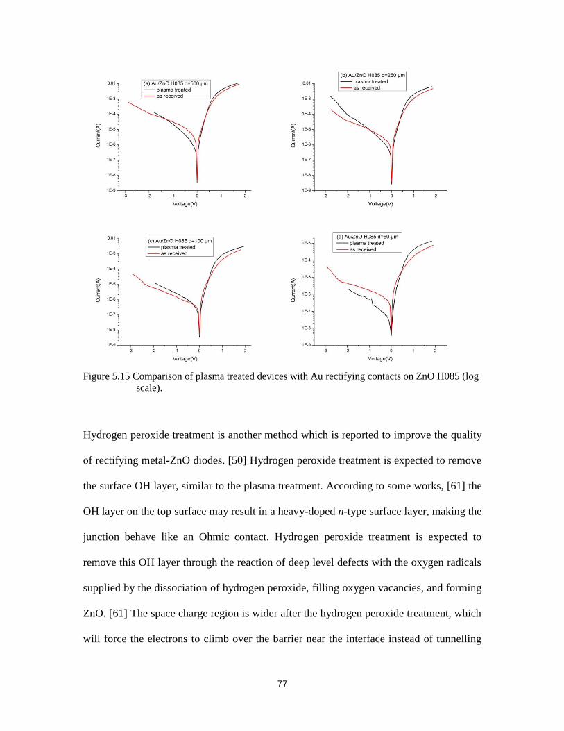


![Synthesis and Characterisation of Lanthanum added ZnO ...joics.org/gallery/ics-1925.pdf · ZnO [26-30]. It clearly shows that the prepared ZnO and La doped ZnO samples revelation](https://static.documents.pub/doc/80x56/5ea23502b68dcf2dd872f588/synthesis-and-characterisation-of-lanthanum-added-zno-joicsorggalleryics-1925pdf.jpg)