San Jose State University San Jose State University SJSU ScholarWorks SJSU ScholarWorks Master's Projects Master's Theses and Graduate Research Spring 2012 Electrocardiogram (ECG/EKG) using FPGA Electrocardiogram (ECG/EKG) using FPGA Vaibhav Desai San Jose State University Follow this and additional works at: https://scholarworks.sjsu.edu/etd_projects Part of the Computer Sciences Commons Recommended Citation Recommended Citation Desai, Vaibhav, "Electrocardiogram (ECG/EKG) using FPGA" (2012). Master's Projects. 238. DOI: https://doi.org/10.31979/etd.kk7h-c84x https://scholarworks.sjsu.edu/etd_projects/238 This Master's Project is brought to you for free and open access by the Master's Theses and Graduate Research at SJSU ScholarWorks. It has been accepted for inclusion in Master's Projects by an authorized administrator of SJSU ScholarWorks. For more information, please contact [email protected].
Transcript
San Jose State University San Jose State University
SJSU ScholarWorks SJSU ScholarWorks
Master's Projects Master's Theses and Graduate Research
Spring 2012
Electrocardiogram (ECG/EKG) using FPGA Electrocardiogram (ECG/EKG) using FPGA
Vaibhav Desai San Jose State University
Follow this and additional works at: https://scholarworks.sjsu.edu/etd_projects
This Master's Project is brought to you for free and open access by the Master's Theses and Graduate Research at SJSU ScholarWorks. It has been accepted for inclusion in Master's Projects by an authorized administrator of SJSU ScholarWorks. For more information, please contact [email protected].
Associate Dean Office of Graduate Studies and Research Date
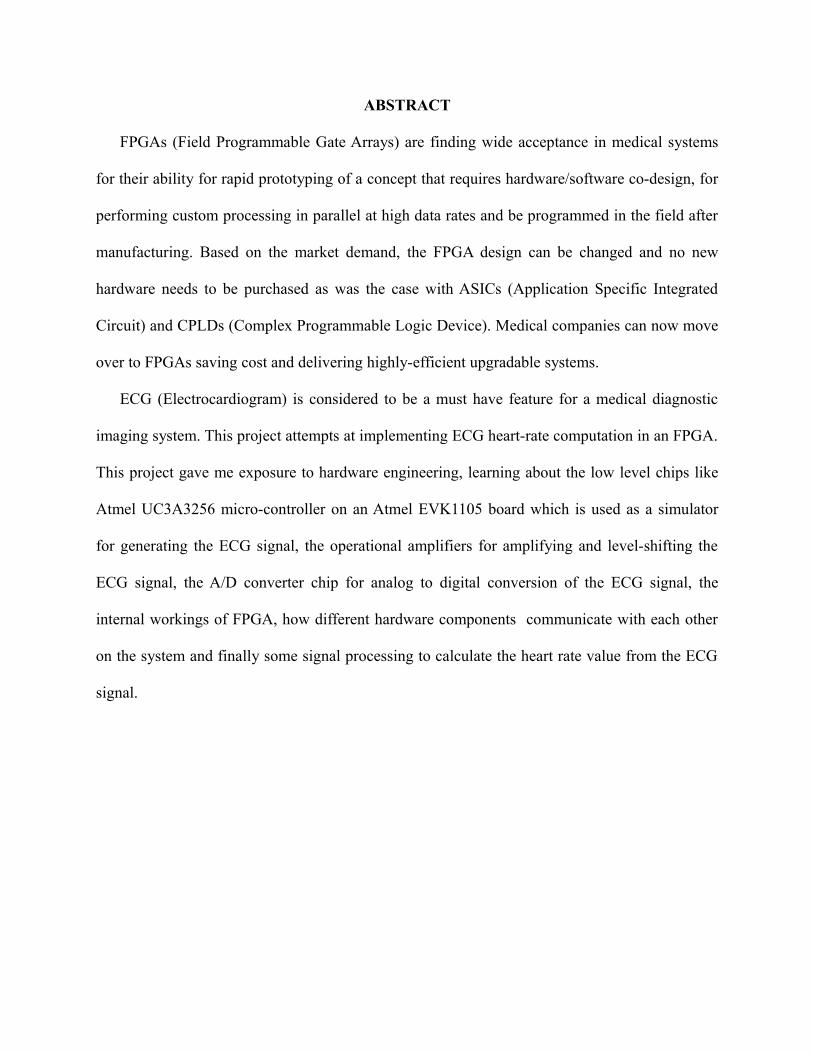
ABSTRACT
FPGAs (Field Programmable Gate Arrays) are finding wide acceptance in medical systems
for their ability for rapid prototyping of a concept that requires hardware/software co-design, for
performing custom processing in parallel at high data rates and be programmed in the field after
manufacturing. Based on the market demand, the FPGA design can be changed and no new
hardware needs to be purchased as was the case with ASICs (Application Specific Integrated
Circuit) and CPLDs (Complex Programmable Logic Device). Medical companies can now move
over to FPGAs saving cost and delivering highly-efficient upgradable systems.
ECG (Electrocardiogram) is considered to be a must have feature for a medical diagnostic
imaging system. This project attempts at implementing ECG heart-rate computation in an FPGA.
This project gave me exposure to hardware engineering, learning about the low level chips like
Atmel UC3A3256 micro-controller on an Atmel EVK1105 board which is used as a simulator
for generating the ECG signal, the operational amplifiers for amplifying and level-shifting the
ECG signal, the A/D converter chip for analog to digital conversion of the ECG signal, the
internal workings of FPGA, how different hardware components communicate with each other
on the system and finally some signal processing to calculate the heart rate value from the ECG
signal.
ACKNOWLEDGEMENTS
I am very grateful to my advisor Dr. Robert Chun for guiding me through this project. His
constant support and patience was vital to the completion of this project. I thank him for
believing in me and encouraging me throughout the course of this project.
I am grateful to Mr. Dan Need for sharing his expertise on FPGA and helping me take the
right decisions. I thank him for taking the time to answer my questions clearly and with patience
during the design phase of the project.
I appreciate the help I received from Mr. Tarak Shah in overcoming all the technical
challenges I faced while working on this project. His knowledge on FPGA systems and their
implementation is exceptional.
Finally, I would like to sincerely thank my committee member Dr. Jon Pearce for his
support. I am also thankful to my friends and family especially Ms. Namrata Bapat who stood by
me throughout this entire journey here at San Jose State University.
Thank you.
Vaibhav Desai
TABLE OF CONTENTS
LIST OF TABLES
LIST OF FIGURES
1. BACKGROUND
This section gives a brief introduction to ECG. Section 1.1 explains what is ECG. Section 1.2
explains the electrical activity of the heart resulting in generation of 5 distinct waves. Finally,
section 1.3 explains how ECG data is interpreted to get the heart rate from the electrical signal.
1.1 WHAT IS ECG
Electrocardiography (ECG/EKG) is a medical diagnostic test that captures the heart’s
electrical workings helping in understanding the rhythm of the heart and any irregularities
associated with it. The result of the test is called an “Electrocardiogram”. The heart muscles
contract due to electrical signals received from the sinoartrial node. These electrical impulses are
detected by an ECG. It is non-evasive and one of the most common procedures a person
undergoes when having any trouble with breathing, chest pain, etc.
1.2 HOW DOES IT WORK
Electrical signals are triggered due to heart muscle depolarization which occurs during every
heartbeat. Each heart muscle cell has a negative charge around it, which is along its membrane
when the heart is at rest. Depolarization is the process of decreasing this negative charge to zero
with the help of cations like Na+ and Ca++. This causes the heart muscles to contract. During
each heartbeat, a healthy heart will have an orderly progression of a wave of depolarization that
is triggered by the cells in the sinoatrial node, spreading out through the atrium, and passing
through the atrioventracular node and then spreading all over the ventricles.
Generally more than two pairs of electrodes are used to detect these signals. The output of a
pair of electrodes is known as lead. Placing more than a pair of electrodes provides a better way
8 | P a g e
to analyze the heart from different angles. Commonly 12 electrodes are used during an ECG,
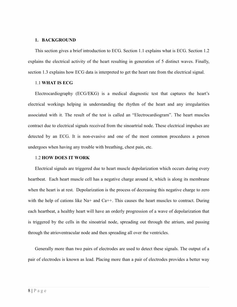
which are placed across the chest, arms and legs. An ECG signal is shown in the figure below:
Figure - Typical ECG signal
• The P wave represents the atrial contractions.• QRS complex represents the ventricular contractions. The R peak indicates a heartbeat.• The T wave is the last common wave in an ECG. This electrical signal is produced when
the ventricles are repolarizing.• The letters used in the ECG signal description do not have abbreviations in medical
terminology.1.3 ECG INTERPRETATION
The output generated by an ECG is in the graph format with time on the x-axis and voltage
on the y-axis. The baseline voltage is known as isoelectric line. In case of no signal detection,
this would be a flat line. QRS complex is a combination of three graphical deflections noted on a
typical ECG. Most of the times, it is the central and most visually obvious part of the trace
generated. An ECG has five deflections, “P” through “T”. The Q, R and S waves occur in rapid
succession and are usually considered together. They reflect a single event but do not necessarily
appear in all leads. Post P wave, the Q wave is a downward deflection. It is followed by the R
wave which is an upward spike. The S wave is again a downward deflection after the R wave. S
wave is followed by the T wave. Modern ECG monitors convert these electrical signals into
9 | P a g e
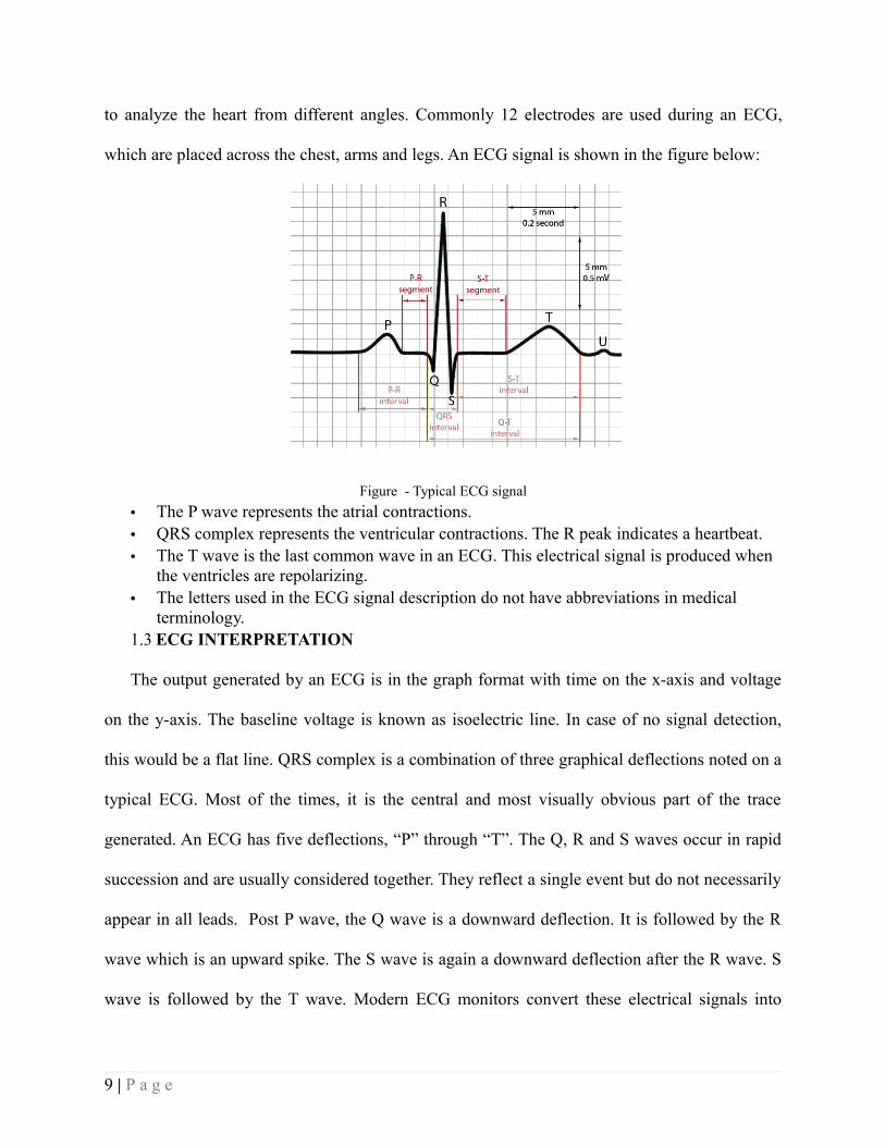
digital values. They make use of various types of filters for signal processing. AN ECG graph as
observed on a Philips ECG system is shown below:
Figure - ECG graph recorded on Philips system
10 | P a g e
2. RELATED WORK
This section discusses the methods that have been used for implementing ECG.
2.1 TRADITIONAL METHOD
The traditional methods involve using leads to detect heart rate. The standard 12-lead
electrocardiogram is a representation of the heart's electrical activity recorded from electrodes on
the body surface. The electrical signals then get passed on to a data logger system that performs
all the necessary signal processing and shows an ECG waveform on the screen. This method is
widely used in diagnostic centers.
2.2 PULSE OXIMETRY
This method uses the principle of light absorbance to determine oxygenated blood from
deoxygenated. In doing so, it then calculates the heart rate and an ECG. Pulse oximetry uses a
sensor which is placed on a sensitive part of the body, usually fingertip or earlobes. The basic
idea is to pass light of two different wavelengths through the body. Typically, light emitting
diodes (LEDs) are used in this process. One emits red light while the other emits infrared light.
The absorption of light depends on the wavelengths as well as the blood inside the human body.
Absorption of radiation as a function of wavelength is calculated. Absorption of both the lights
differs significantly for oxygenated and deoxygenated blood as it depends on the amount of
oxygen present. Based on it, the device can determine a heartbeat or a pulse. In smartphone apps,
the camera is used to emit light. Placing one’s fingertip on the camera is same as placing it on a
sensor of a pulse oximetry device. The app triggers the phone to emit light of certain
wavelengths and then calculates the heart rate.
11 | P a g e
2.3 SEISMOCARDIOGRAPHY
Seismocardiogram (SCG) is the recording of body vibrations that are induced by the human
heart. SCG can provide definitive information about cardiac output. It uses accelerometer to
determine the pace or change of pace in the vibrations. SCG with the help of accelerometers can
help establish heart rate by assessing respiratory movements. Accelerometers can be attached
directly to human body using inertial footpads or by attaching it to some fabric. They are
commonly used on treadmills.
12 | P a g e
3. SYSTEM COMPONENTS
This section discusses the individual components used in the implementation of ECG using
FPGA.
3.1 DEVELOPMENT BOARD - ALTERA DE2 115
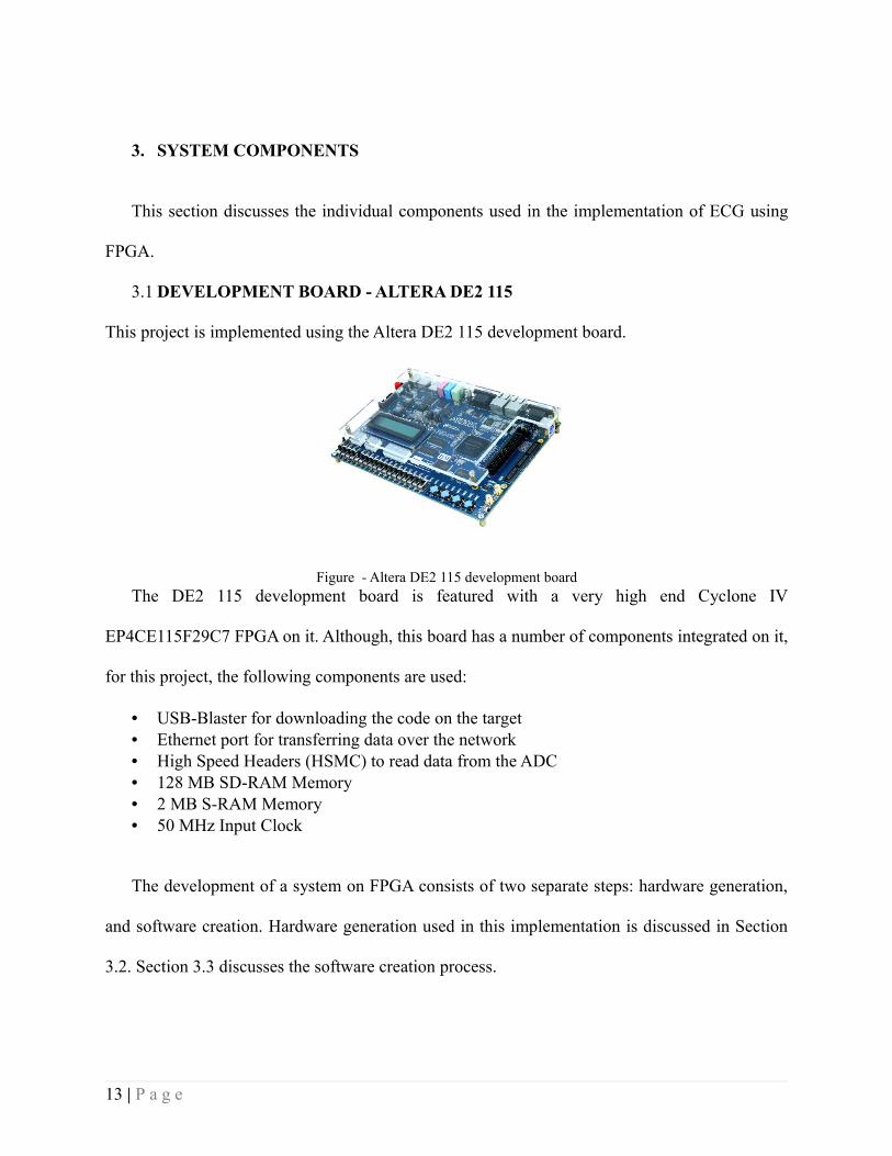
This project is implemented using the Altera DE2 115 development board.
Figure - Altera DE2 115 development boardThe DE2 115 development board is featured with a very high end Cyclone IV
EP4CE115F29C7 FPGA on it. Although, this board has a number of components integrated on it,
for this project, the following components are used:
• USB-Blaster for downloading the code on the target • Ethernet port for transferring data over the network • High Speed Headers (HSMC) to read data from the ADC• 128 MB SD-RAM Memory• 2 MB S-RAM Memory• 50 MHz Input Clock
The development of a system on FPGA consists of two separate steps: hardware generation,
and software creation. Hardware generation used in this implementation is discussed in Section
3.2. Section 3.3 discusses the software creation process.
13 | P a g e
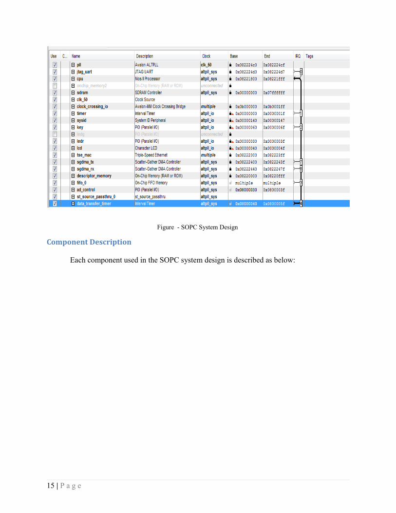
3.2 HARDWARE GENERATION - SOPC
SOPC Builder is software provided by Altera that allows creating soft-hardware components
by generating the corresponding Verilog or VHDL files in the background. This eases the
development efforts and helps in focusing on the application logic. In this case, the software was
used to create a system that will use the NIOS II soft-core processor from Altera.
SOPC Builder automates the task of integrating hardware components. Using traditional design
methods, the developer manually writes HDL modules to wire together the pieces of the system.
SOPC Builder generates the interconnect logic automatically as components are added to the
system. SOPC Builder generates HDL files that define all components of the system, and a top-
level HDL file that connects all the components together. SOPC Builder generates either Verilog
HDL or VHDL equally. In this project, the focus was only on the Verilog files. It produces low-
level drivers for accessing the hardware and adds an API layer on top of these drivers which can
be easily called from the software. The following figure shows the SOPC system design for the
project:
14 | P a g e
Figure - SOPC System Design
Component Description
Each component used in the SOPC system design is described as below:
15 | P a g e
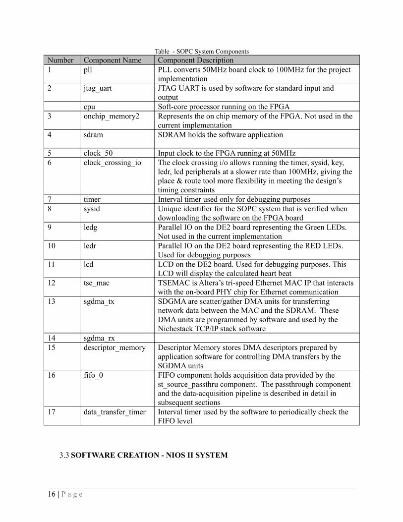
Table - SOPC System Components
Number Component Name Component Description1 pll PLL converts 50MHz board clock to 100MHz for the project
implementation2 jtag_uart JTAG UART is used by software for standard input and
outputcpu Soft-core processor running on the FPGA
3 onchip_memory2 Represents the on chip memory of the FPGA. Not used in the current implementation
4 sdram SDRAM holds the software application
5 clock_50 Input clock to the FPGA running at 50MHz6 clock_crossing_io The clock crossing i/o allows running the timer, sysid, key,
ledr, lcd peripherals at a slower rate than 100MHz, giving the place & route tool more flexibility in meeting the design’s timing constraints
7 timer Interval timer used only for debugging purposes8 sysid Unique identifier for the SOPC system that is verified when
downloading the software on the FPGA board9 ledg Parallel IO on the DE2 board representing the Green LEDs.
Not used in the current implementation10 ledr Parallel IO on the DE2 board representing the RED LEDs.
Used for debugging purposes11 lcd LCD on the DE2 board. Used for debugging purposes. This
LCD will display the calculated heart beat12 tse_mac TSEMAC is Altera’s tri-speed Ethernet MAC IP that interacts
with the on-board PHY chip for Ethernet communication13 sgdma_tx SDGMA are scatter/gather DMA units for transferring
network data between the MAC and the SDRAM. These DMA units are programmed by software and used by the Nichestack TCP/IP stack software
14 sgdma_rx15 descriptor_memory Descriptor Memory stores DMA descriptors prepared by
application software for controlling DMA transfers by the SGDMA units
16 fifo_0 FIFO component holds acquisition data provided by the st_source_passthru component. The passthrough component and the data-acquisition pipeline is described in detail in subsequent sections
17 data_transfer_timer Interval timer used by the software to periodically check the FIFO level
3.3 SOFTWARE CREATION - NIOS II SYSTEM
16 | P a g e
Nios II is a 32-bit embedded soft-core processor architecture designed by Altera for use in
Altera’s FPGAs. Nios II is based on the RISC architecture and is implemented using the logic
blocks on the FPGA. It is available in three different flavors: Nios II/f (fast), Nios II/s (standard)
and Nios II/e (economy). For Nios II software development, Altera provides Embedded Design
Suite (EDS), an Integrated Development Environment (IDE) written on top of Eclipse which
includes C/C++ compiler. EDS supports run-time debugging in a simulation mode, thereby
saving the compile time and download time for the target FPGA. A stable system design with the
Nios II software can then be downloaded on the target.
This project was first implemented using the economic edition of Nios II since it
provided support for in-depth debugging. Once the major bugs were eliminated from the project
and the performance benchmarks were set, the Nios II economic edition was replaced by the
Nios II fast edition. Also, no calls were made to the C++’s standard input output library since
these are expensive calls for the Nios II processor.
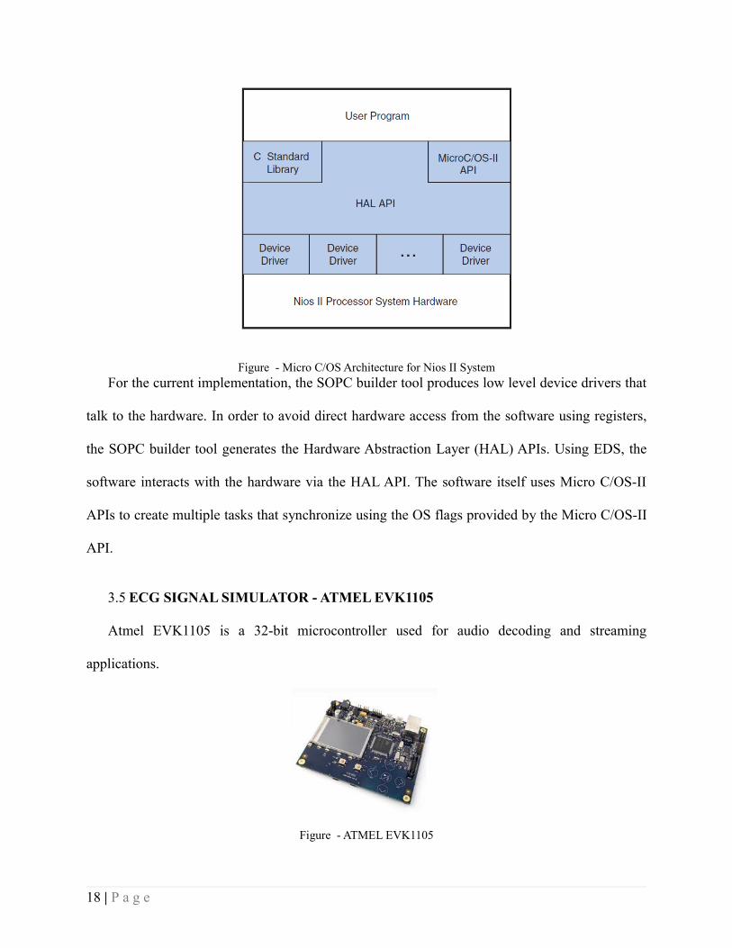
3.4 MICRO C/OS-II
Micro-Controller Operating System, known as Micro C/OS-II is a Real Time Operating
System (RTOS) supporting multi-tasking capabilities. Its light weight kernel makes it the evident
choice for use in embedded systems. In the context of the project, this OS is selected for its
ability to support multiple tasks and allow inter-task communication. Semaphores and mailbox
cores are used for task signaling and task synchronization. The following figure shows how the
Micro C/OS-II APIs integrate with the FPGA.
17 | P a g e
Figure - Micro C/OS Architecture for Nios II SystemFor the current implementation, the SOPC builder tool produces low level device drivers that
talk to the hardware. In order to avoid direct hardware access from the software using registers,
the SOPC builder tool generates the Hardware Abstraction Layer (HAL) APIs. Using EDS, the
software interacts with the hardware via the HAL API. The software itself uses Micro C/OS-II
APIs to create multiple tasks that synchronize using the OS flags provided by the Micro C/OS-II
API.
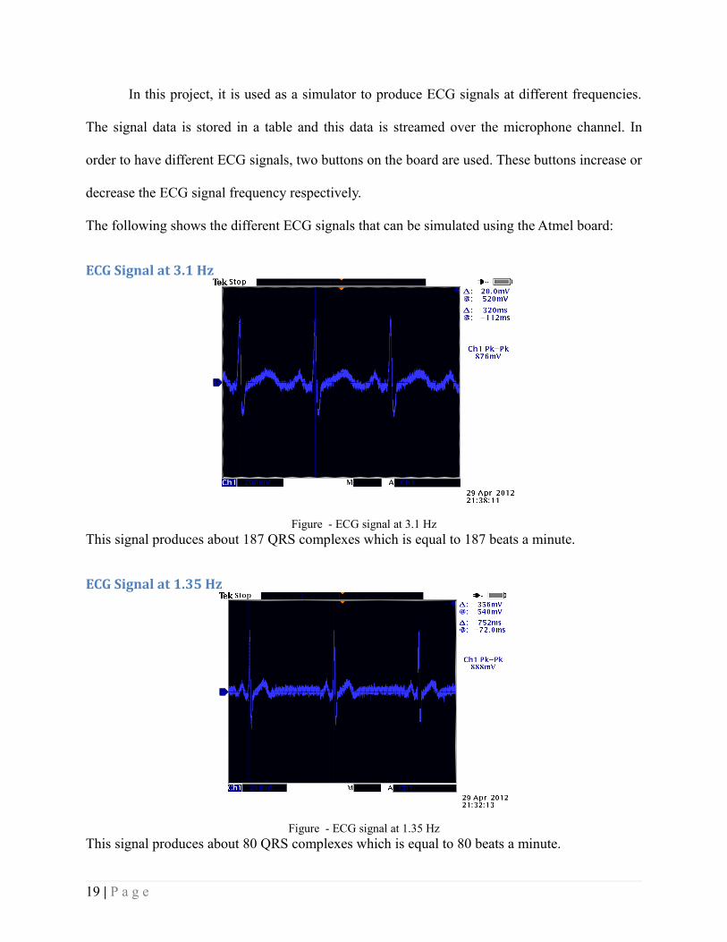
3.5 ECG SIGNAL SIMULATOR - ATMEL EVK1105
Atmel EVK1105 is a 32-bit microcontroller used for audio decoding and streaming
applications.
Figure - ATMEL EVK1105
18 | P a g e
In this project, it is used as a simulator to produce ECG signals at different frequencies.
The signal data is stored in a table and this data is streamed over the microphone channel. In
order to have different ECG signals, two buttons on the board are used. These buttons increase or
decrease the ECG signal frequency respectively.
The following shows the different ECG signals that can be simulated using the Atmel board:
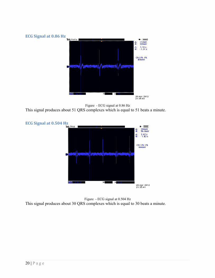
ECG Signal at 3.1 Hz
Figure - ECG signal at 3.1 HzThis signal produces about 187 QRS complexes which is equal to 187 beats a minute.
ECG Signal at 1.35 Hz
Figure - ECG signal at 1.35 HzThis signal produces about 80 QRS complexes which is equal to 80 beats a minute.
19 | P a g e
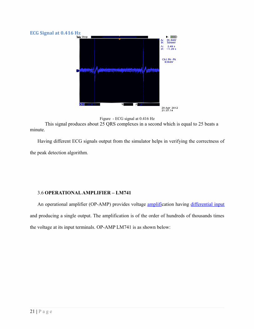
ECG Signal at 0.86 Hz
Figure - ECG signal at 0.86 HzThis signal produces about 51 QRS complexes which is equal to 51 beats a minute.
ECG Signal at 0.504 Hz
Figure - ECG signal at 0.504 HzThis signal produces about 30 QRS complexes which is equal to 30 beats a minute.
20 | P a g e
ECG Signal at 0.416 Hz
Figure - ECG signal at 0.416 HzThis signal produces about 25 QRS complexes in a second which is equal to 25 beats a
minute.
Having different ECG signals output from the simulator helps in verifying the correctness of
the peak detection algorithm.
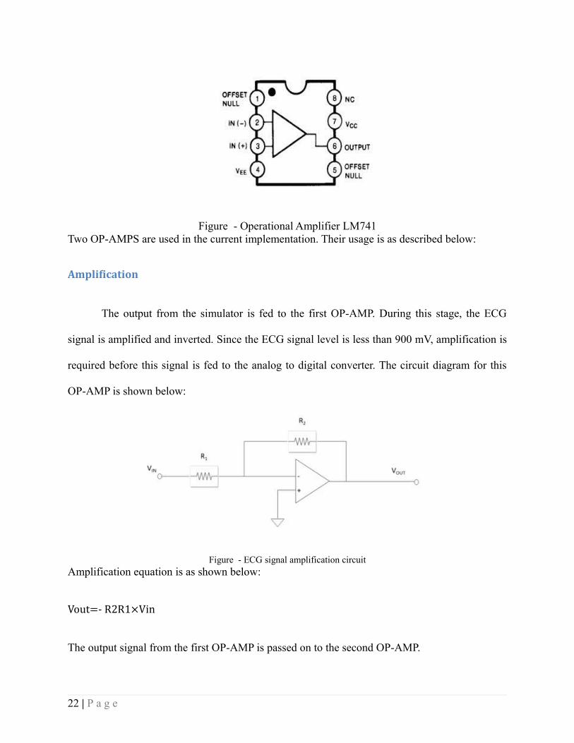
3.6 OPERATIONAL AMPLIFIER – LM741
An operational amplifier (OP-AMP) provides voltage amplification having differential input
and producing a single output. The amplification is of the order of hundreds of thousands times
the voltage at its input terminals. OP-AMP LM741 is as shown below:
Figure - Operational Amplifier LM741Two OP-AMPS are used in the current implementation. Their usage is as described below:
Amplification
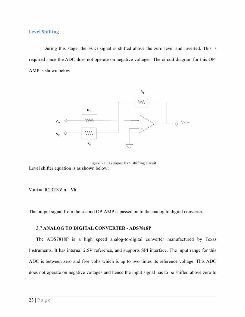
The output from the simulator is fed to the first OP-AMP. During this stage, the ECG
signal is amplified and inverted. Since the ECG signal level is less than 900 mV, amplification is
required before this signal is fed to the analog to digital converter. The circuit diagram for this
OP-AMP is shown below:
Figure - ECG signal amplification circuitAmplification equation is as shown below:
Vout=- R2R1×VinThe output signal from the first OP-AMP is passed on to the second OP-AMP.
22 | P a g e
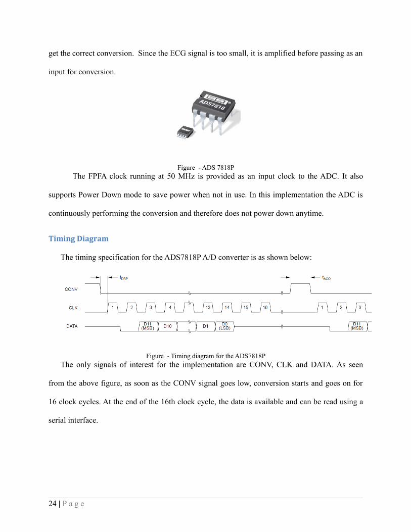
Level Shifting
During this stage, the ECG signal is shifted above the zero level and inverted. This is
required since the ADC does not operate on negative voltages. The circuit diagram for this OP-
AMP is shown below:
Figure - ECG signal level shifting circuitLevel shifter equation is as shown below:
Vout=- R1R2×Vin+ VkThe output signal from the second OP-AMP is passed on to the analog to digital converter.
3.7 ANALOG TO DIGITAL CONVERTER - ADS7818P
The ADS7818P is a high speed analog-to-digital converter manufactured by Texas
Instruments. It has internal 2.5V reference, and supports SPI interface. The input range for this
ADC is between zero and five volts which is up to two times its reference voltage. This ADC
does not operate on negative voltages and hence the input signal has to be shifted above zero to
23 | P a g e
get the correct conversion. Since the ECG signal is too small, it is amplified before passing as an
input for conversion.
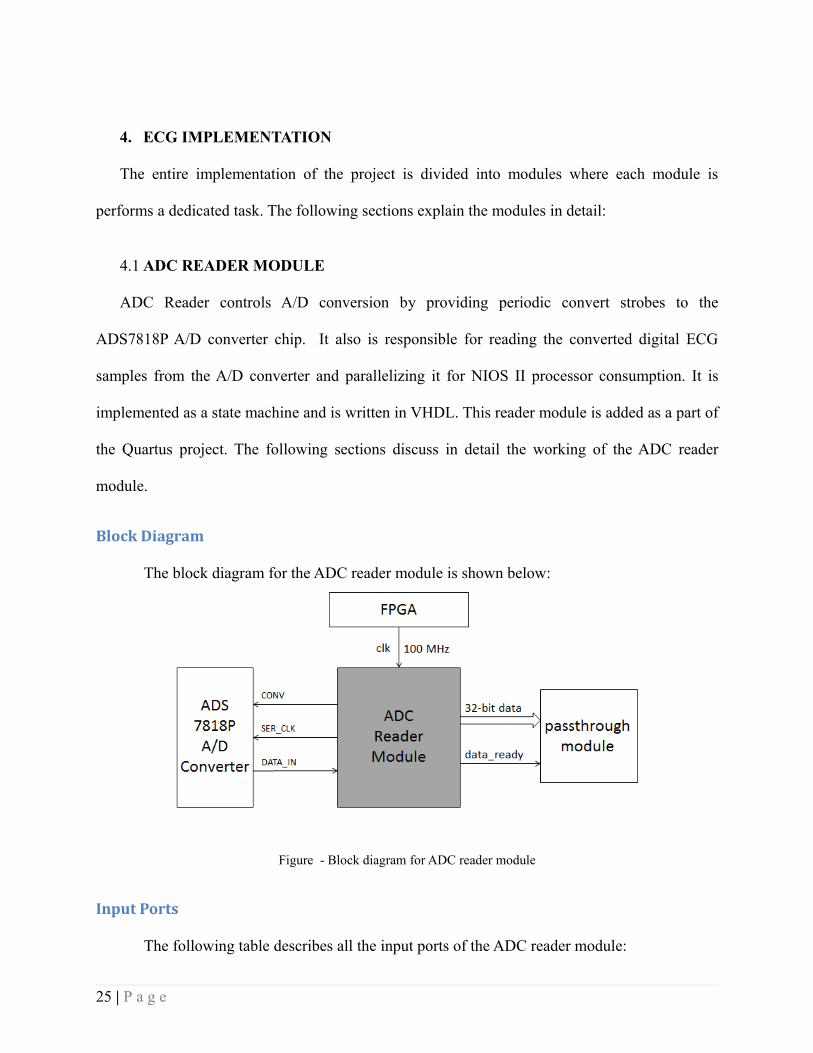
Figure - ADS 7818PThe FPFA clock running at 50 MHz is provided as an input clock to the ADC. It also
supports Power Down mode to save power when not in use. In this implementation the ADC is
continuously performing the conversion and therefore does not power down anytime.
Timing Diagram
The timing specification for the ADS7818P A/D converter is as shown below:
Figure - Timing diagram for the ADS7818PThe only signals of interest for the implementation are CONV, CLK and DATA. As seen
from the above figure, as soon as the CONV signal goes low, conversion starts and goes on for
16 clock cycles. At the end of the 16th clock cycle, the data is available and can be read using a
serial interface.
24 | P a g e
4. ECG IMPLEMENTATION
The entire implementation of the project is divided into modules where each module is
performs a dedicated task. The following sections explain the modules in detail:
4.1 ADC READER MODULE
ADC Reader controls A/D conversion by providing periodic convert strobes to the
ADS7818P A/D converter chip. It also is responsible for reading the converted digital ECG
samples from the A/D converter and parallelizing it for NIOS II processor consumption. It is
implemented as a state machine and is written in VHDL. This reader module is added as a part of
the Quartus project. The following sections discuss in detail the working of the ADC reader
module.
Block Diagram
The block diagram for the ADC reader module is shown below:
Figure - Block diagram for ADC reader module
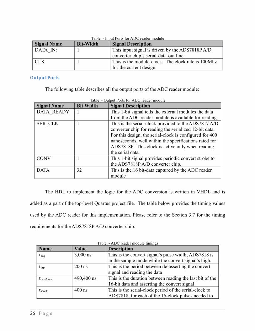
Input Ports
The following table describes all the input ports of the ADC reader module:
25 | P a g e
Table - Input Ports for ADC reader module
Signal Name Bit-Width Signal DescriptionDATA_IN: 1 This input signal is driven by the ADS7818P A/D
converter chip’s serial-data-out line.CLK 1 This is the module-clock. The clock rate is 100Mhz
for the current design.
Output Ports
The following table describes all the output ports of the ADC reader module:
Table - Output Ports for ADC reader module
Signal Name Bit Width Signal DescriptionDATA_READY 1 This 1-bit signal tells the external modules the data
from the ADC reader module is available for readingSER_CLK 1 This is the serial-clock provided to the ADS7817 A/D
converter chip for reading the serialized 12-bit data. For this design, the serial-clock is configured for 400 nanoseconds, well within the specifications rated for ADS7818P. This clock is active only when reading the serial data.
CONV 1 This 1-bit signal provides periodic convert strobe to the ADS7818P A/D converter chip.
DATA 32 This is the 16 bit-data captured by the ADC reader module
The HDL to implement the logic for the ADC conversion is written in VHDL and is
added as a part of the top-level Quartus project file. The table below provides the timing values
used by the ADC reader for this implementation. Please refer to the Section 3.7 for the timing
requirements for the ADS7818P A/D converter chip.
Table - ADC reader module timings
Name Value Descriptiontacq 3,000 ns This is the convert signal’s pulse width; ADS7818 is
in the sample mode while the convert signal’s high.tdrp 200 ns This is the period between de-asserting the convert
signal and reading the datatdata2conv 490,400 ns This is the duration between reading the last bit of the
16-bit data and asserting the convert signaltserclk 400 ns This is the serial-clock period of the serial-clock to
ADS7818, for each of the 16-clock pulses needed to
26 | P a g e
pull the 16 bits of data.
Based on the values listed in the table below, this design obtains ECG sampled data,
periodically, every 500,000 microseconds.
State Machine
The following diagram shows the state machine representation of this module. This state
machine is synchronous to the module’s input clock, running at 100MHz. It uses an internal
counter to generate the slower serial clock needed by the ADS7818P A/D converter chip.
27 | P a g e
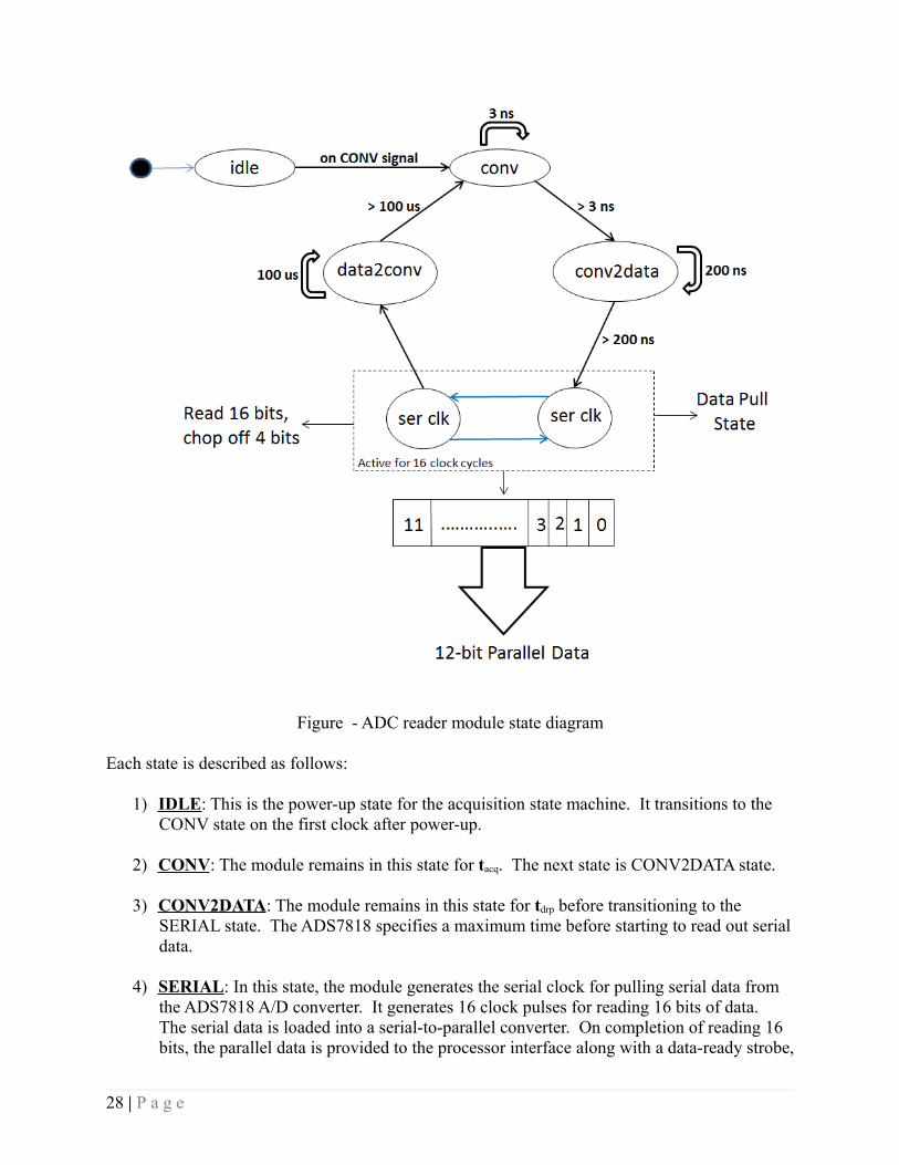
Figure - ADC reader module state diagram
Each state is described as follows:
1) IDLE : This is the power-up state for the acquisition state machine. It transitions to the CONV state on the first clock after power-up.
2) CONV : The module remains in this state for tacq. The next state is CONV2DATA state.
3) CONV2DATA : The module remains in this state for tdrp before transitioning to the SERIAL state. The ADS7818 specifies a maximum time before starting to read out serial data.
4) SERIAL : In this state, the module generates the serial clock for pulling serial data from the ADS7818 A/D converter. It generates 16 clock pulses for reading 16 bits of data. The serial data is loaded into a serial-to-parallel converter. On completion of reading 16 bits, the parallel data is provided to the processor interface along with a data-ready strobe,
28 | P a g e
informing the receiving interface that data’s ready. The data remains valid till the next conversion is read. The data-ready strobe is a single-clock wide pulse. The module then enters the DATA2CONV state. ADS7818P specifications provide a lower limit to the serial-clock rate.
5) DATA2CONV : This state is an idle state that allows reducing the acquisition rate while not violating the other timing parameters affecting the other states.
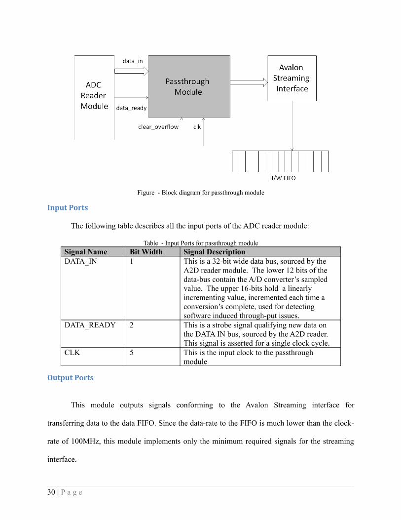
4.2 PASSTHROUGH MODULE
This module is responsible for transferring the acquisition data from the generic-interface of
the A2D reader module to the Avalon-streaming interfaced data FIFO. The rationale for
introducing this adapter is to keep the A2D reader module with a generic interface for
component-reuse in designs that may not conform to Altera-streaming interface. As soon as the
DATA_READY is set by the ADC reader module, this module reads all the data and makes the
same data available to the Altera Avalon streaming interface. Once the right bits are set, the
Avalon streaming interface reads the data and pushes it on the FIFO.
The following sections discuss in detail the working of the passthrough module:
Block Diagram
The block diagram for the passthrough module is as shown below:
29 | P a g e
Figure - Block diagram for passthrough module
Input Ports
The following table describes all the input ports of the ADC reader module:
Table - Input Ports for passthrough module
Signal Name Bit Width Signal DescriptionDATA_IN 1 This is a 32-bit wide data bus, sourced by the
A2D reader module. The lower 12 bits of the data-bus contain the A/D converter’s sampled value. The upper 16-bits hold a linearly incrementing value, incremented each time a conversion’s complete, used for detecting software induced through-put issues.
DATA_READY 2 This is a strobe signal qualifying new data on the DATA IN bus, sourced by the A2D reader. This signal is asserted for a single clock cycle.
CLK 5 This is the input clock to the passthrough module
Output Ports
This module outputs signals conforming to the Avalon Streaming interface for
transferring data to the data FIFO. Since the data-rate to the FIFO is much lower than the clock-
rate of 100MHz, this module implements only the minimum required signals for the streaming
interface.
30 | P a g e
4.3 HARDWARE FIFO
Altera provides a hardware based FIFO on its on-chip memory region. This hardware FIFO
can buffer data and help in the flow control for the SOPC system. Single clock or separate clocks
can be used to operate this FIFO but this implementation uses a single clock input. An interrupt
can be generated when the FIFO level reaches a user-defined threshold. Here an interval timer is
used that queries this level periodically to determine if there are enough packets available to be
transferred over the network via the UDP protocol. The FIFO level is queried using an interface
altera_avalon_fifo_read_level( ) provided in the low-level driver generated by the SOPC system
and the contents of the FIFO are read using the function altera_avalon_read_fifo( ).
FIFO Usage
The FIFO is configured to be of 8K levels which mean the FIFO can store up to 8192
samples from the ADS7818P A/D converter chip at any time. The ADC runs continuously
converting the analog input to digital data and storing it in the FIFO. The rate at which ADC
writes data to the FIFO is synchronized with the rate at which the software reads data from the
FIFO. This ensures that there is enough memory available in the FIFO at all times. If the FIFO is
full, the ADC will stop pushing data on the FIFO, no existing samples of the FIFO are over-
written. There is no mechanism to handle this scenario and the software will come to an halt.
4.4 INTERVAL TIMER
Altera provides a hardware based Interval Timer core with the Altera DE-2 115 board. An
Interrupt Request (IRQ) is generated every time the timer expires. This timer is implemented as a
simple counter internally using the clock period of the FPGA. An Interrupt Service Routine
31 | P a g e
(ISR) has to be registered with the IRQ at the program startup as a callback method. Every time,
the timer reaches zero, it generates an IRQ that is handled by the ISR. The timer can be reset or
disabled from the ISR. The timer supports the following features:
1) Timeout period up to 1 microsecond.
2) Can be controlled using the NIOS II system
3) Can be level-triggered or edge-triggered. For this project, level-triggered mode is used for
the timer.
4) Optional watchdog to check if the timer reached to zero. Watchdog is not used in the
current implementation.
Timer ISR Implementation
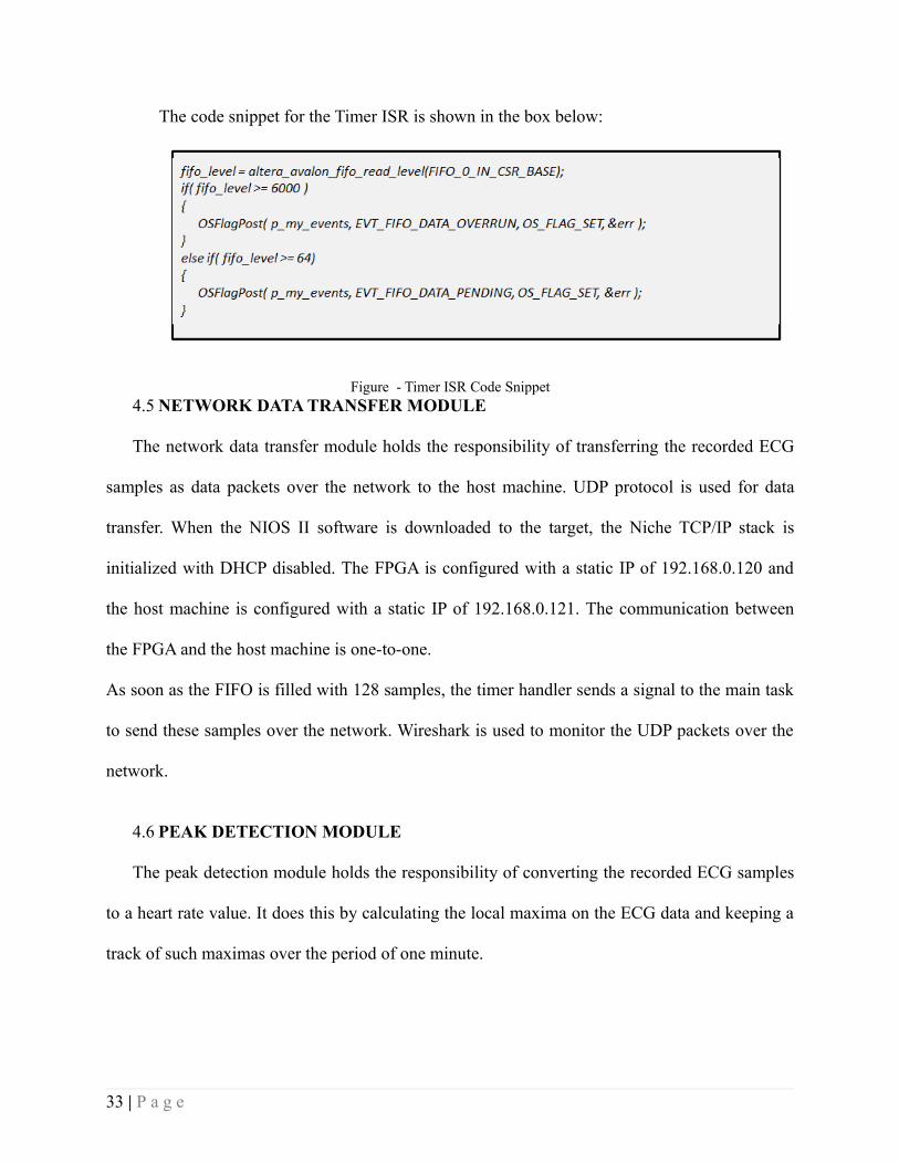
When the timer reaches zero, the ISR function TimerISR() gets invoked. This function does
the following:
1) Read the current hardware FIFO level.
2) If the level is greater than 64, set the OS flag EVT_FIFO_DATA_PENDING. This
internally sends a signal to the other network task indicating data is available in the FIFO.
That task reads the data from the FIFO and sends it over the network via the UDP
protocol.
3) If the level is greater than 6000, set the OS flag EVT_FIFO_DTA_OVERRUN. Based on
the timer interval and the rate at which the ADC is producing digital data, this condition
will never be hit. This is only for debugging purposes.
4) Reset the timer
Timer ISR Code Snippet
32 | P a g e
The code snippet for the Timer ISR is shown in the box below:
Figure - Timer ISR Code Snippet4.5 NETWORK DATA TRANSFER MODULE
The network data transfer module holds the responsibility of transferring the recorded ECG
samples as data packets over the network to the host machine. UDP protocol is used for data
transfer. When the NIOS II software is downloaded to the target, the Niche TCP/IP stack is
initialized with DHCP disabled. The FPGA is configured with a static IP of 192.168.0.120 and
the host machine is configured with a static IP of 192.168.0.121. The communication between
the FPGA and the host machine is one-to-one.
As soon as the FIFO is filled with 128 samples, the timer handler sends a signal to the main task
to send these samples over the network. Wireshark is used to monitor the UDP packets over the
network.
4.6 PEAK DETECTION MODULE
The peak detection module holds the responsibility of converting the recorded ECG samples
to a heart rate value. It does this by calculating the local maxima on the ECG data and keeping a
track of such maximas over the period of one minute.
33 | P a g e
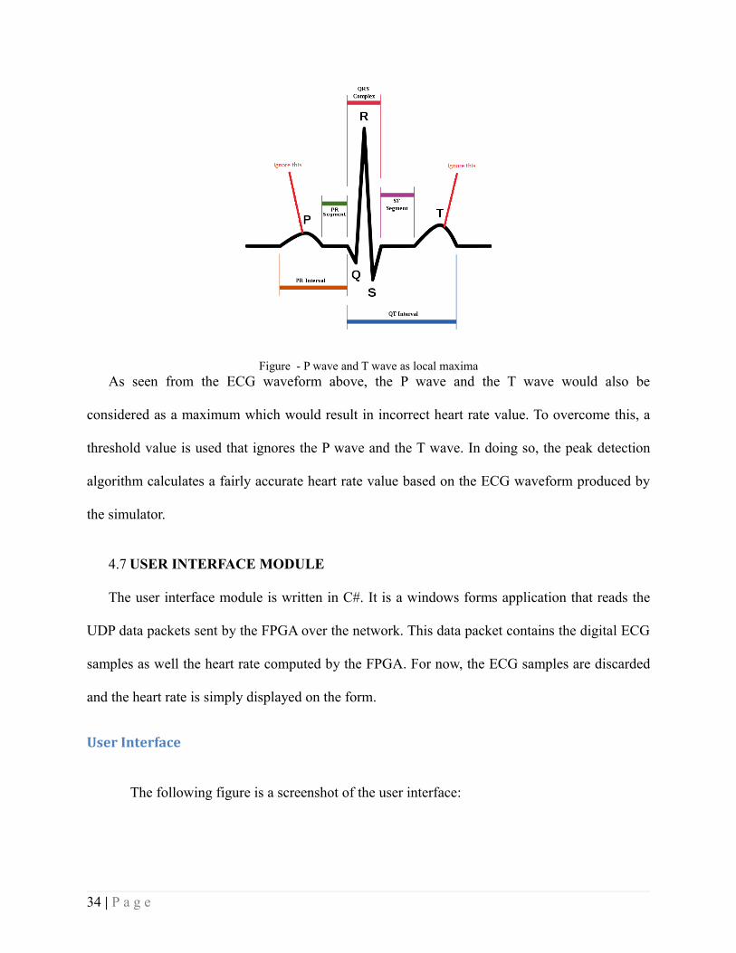
Figure - P wave and T wave as local maximaAs seen from the ECG waveform above, the P wave and the T wave would also be
considered as a maximum which would result in incorrect heart rate value. To overcome this, a
threshold value is used that ignores the P wave and the T wave. In doing so, the peak detection
algorithm calculates a fairly accurate heart rate value based on the ECG waveform produced by
the simulator.
4.7 USER INTERFACE MODULE
The user interface module is written in C#. It is a windows forms application that reads the
UDP data packets sent by the FPGA over the network. This data packet contains the digital ECG
samples as well the heart rate computed by the FPGA. For now, the ECG samples are discarded
and the heart rate is simply displayed on the form.
User Interface
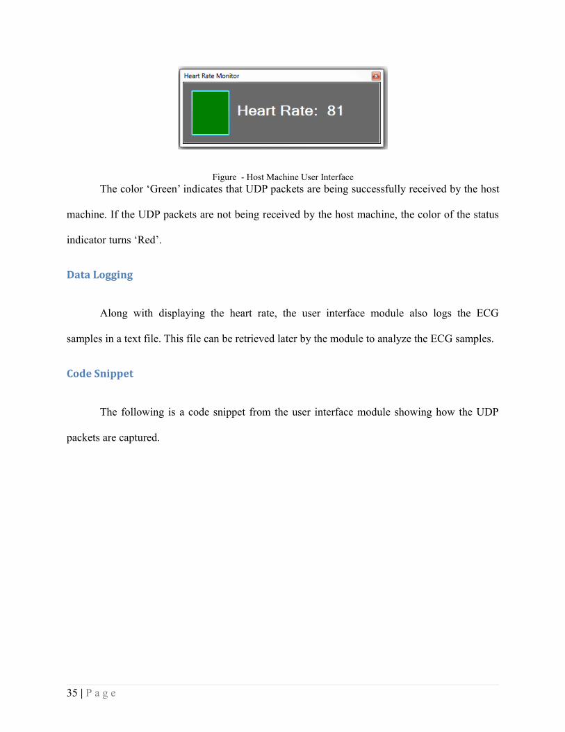
The following figure is a screenshot of the user interface:
34 | P a g e
Figure - Host Machine User InterfaceThe color ‘Green’ indicates that UDP packets are being successfully received by the host
machine. If the UDP packets are not being received by the host machine, the color of the status
indicator turns ‘Red’.
Data Logging
Along with displaying the heart rate, the user interface module also logs the ECG
samples in a text file. This file can be retrieved later by the module to analyze the ECG samples.
Code Snippet
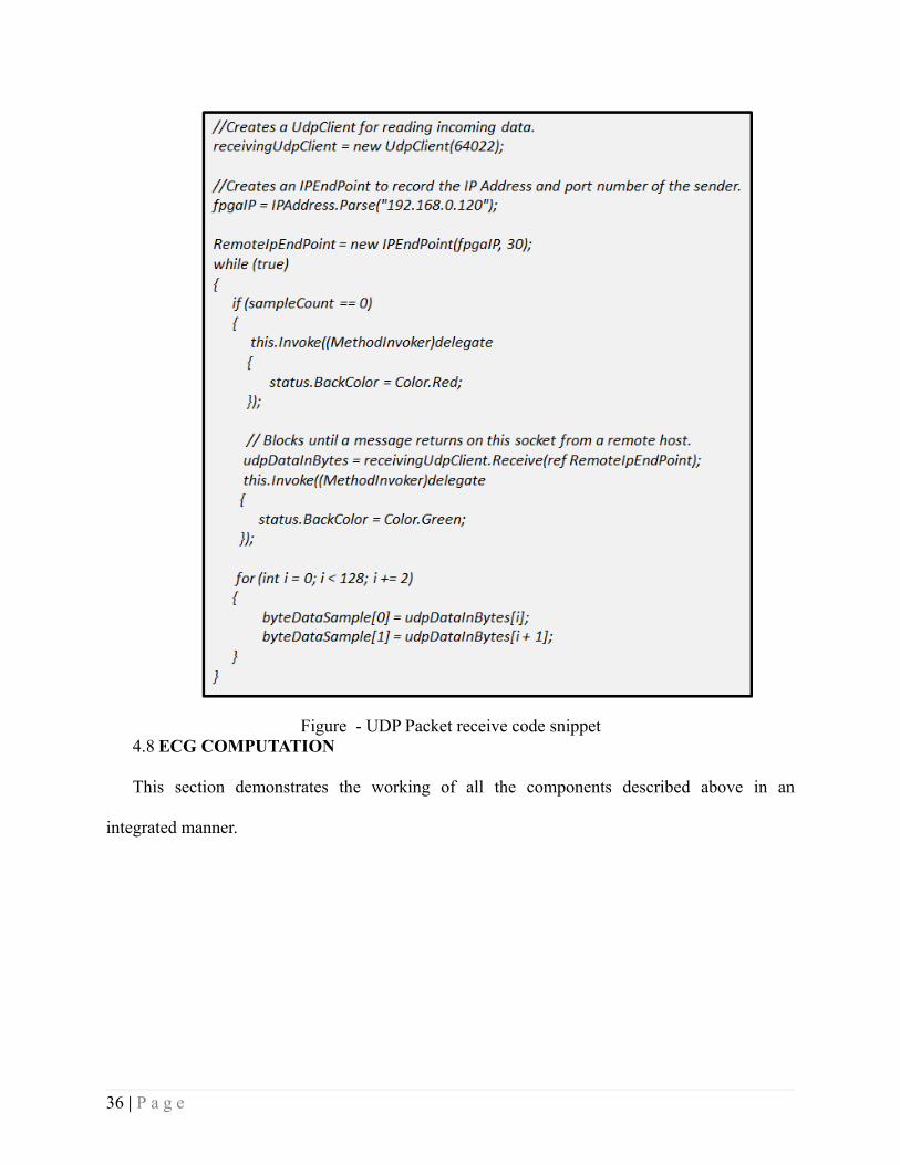
The following is a code snippet from the user interface module showing how the UDP
This section demonstrates the working of all the components described above in an
integrated manner.
36 | P a g e
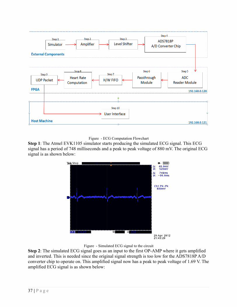
Figure - ECG Computation FlowchartStep 1: The Atmel EVK1105 simulator starts producing the simulated ECG signal. This ECG signal has a period of 748 milliseconds and a peak to peak voltage of 880 mV. The original ECG signal is as shown below:
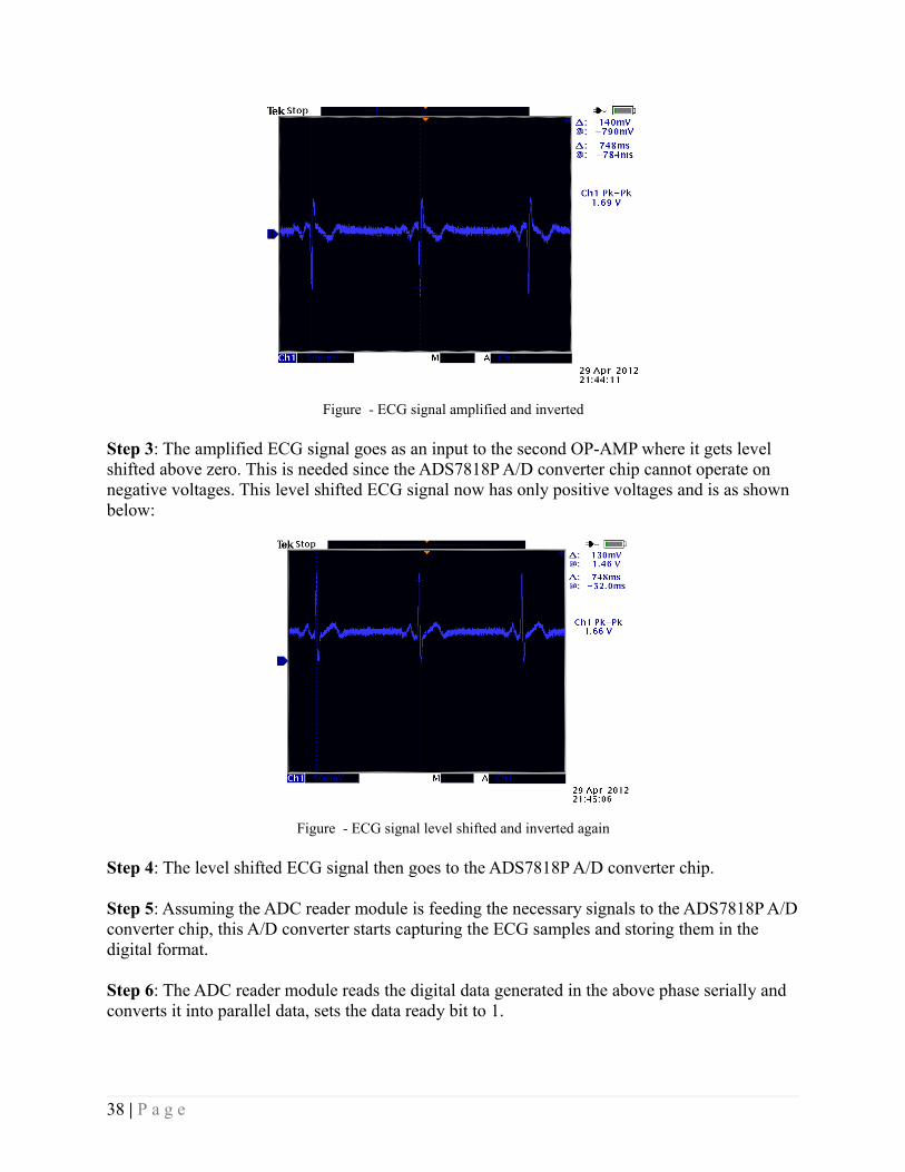
Figure - Simulated ECG signal to the circuitStep 2: The simulated ECG signal goes as an input to the first OP-AMP where it gets amplified and inverted. This is needed since the original signal strength is too low for the ADS7818P A/D converter chip to operate on. This amplified signal now has a peak to peak voltage of 1.69 V. The amplified ECG signal is as shown below:
37 | P a g e
Figure - ECG signal amplified and inverted
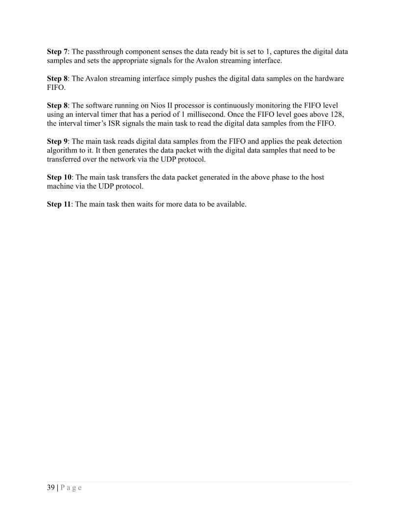
Step 3: The amplified ECG signal goes as an input to the second OP-AMP where it gets level shifted above zero. This is needed since the ADS7818P A/D converter chip cannot operate on negative voltages. This level shifted ECG signal now has only positive voltages and is as shown below:
Figure - ECG signal level shifted and inverted again
Step 4: The level shifted ECG signal then goes to the ADS7818P A/D converter chip.
Step 5: Assuming the ADC reader module is feeding the necessary signals to the ADS7818P A/D converter chip, this A/D converter starts capturing the ECG samples and storing them in the digital format.
Step 6: The ADC reader module reads the digital data generated in the above phase serially and converts it into parallel data, sets the data ready bit to 1.
38 | P a g e
Step 7: The passthrough component senses the data ready bit is set to 1, captures the digital data samples and sets the appropriate signals for the Avalon streaming interface.
Step 8: The Avalon streaming interface simply pushes the digital data samples on the hardware FIFO.
Step 8: The software running on Nios II processor is continuously monitoring the FIFO level using an interval timer that has a period of 1 millisecond. Once the FIFO level goes above 128, the interval timer’s ISR signals the main task to read the digital data samples from the FIFO.
Step 9: The main task reads digital data samples from the FIFO and applies the peak detection algorithm to it. It then generates the data packet with the digital data samples that need to be transferred over the network via the UDP protocol.
Step 10: The main task transfers the data packet generated in the above phase to the host machine via the UDP protocol.
Step 11: The main task then waits for more data to be available.
39 | P a g e
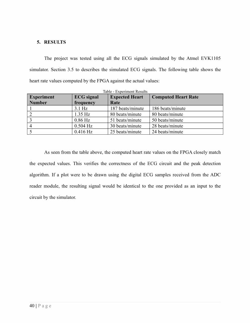
5. RESULTS
The project was tested using all the ECG signals simulated by the Atmel EVK1105
simulator. Section 3.5 to describes the simulated ECG signals. The following table shows the
heart rate values computed by the FPGA against the actual values: