Electrochemical Etching of Zinc Oxide for Silicon Thin Film Solar Cell Applications
S. E. Pusta, J. Worbsa, J. Hüpkesa, S. O. Klemmb, and K. J. J. Mayrhoferb
a Forschungszentrum Jülich GmbH, IEK5 – Photovoltaik, 52425 Jülich, Germany
b Max-Planck-Institut für Eisenforschung GmbH, Max-Planck-Str. 1, 40237 Düsseldorf, Germany
A novel approach is presented for introducing a surface morphology with beneficial light scattering properties to sputter-deposited ZnO:Al films, being used as front contact in Si thin film photovoltaic devices. Electrochemical anodization was used to trigger local corrosion, leading to interfacial structures comple-mentary to those commonly prepared by an etching step in diluted HCl. By systematic variation of electrochemical etching conditions and electrolytes, sensible experimental parameters were evaluated for the preparation of ZnO films that can be applied in Si thin film solar cells. The prepared films were characterized by scanning electron microscopy, four-point resistance and Hall measurements. Furthermore, the kinetics of the heterogeneous interfacial reaction during the corrosion process were studied utilizing electro-analytical techniques. This allowed the identification of the processes occurring at the solid/liquid interface. Application of such films in microcrystalline Si single junction solar cells has shown promising initial results.
Introduction Silicon thin film solar cells require a highly transparent front contact with low series resistance. The most commonly applied transparent conductive oxide (TCO) materials for thin film solar cells are SnO2:In, SnO2:F, ZnO:Al, and ZnO:B (1). The optimization of these TCO films has proven to be crucial for high cell efficiency (2). In superstrate configuration, the interface between the TCO and Si must provide a certain roughness for light scattering as to trap the light in the solar cell by continuous reflection within the absorber layer. With sputter-deposited ZnO:Al, this roughness is usually achieved in a chemical etching step with diluted HCl (3). This process is leading to the so-called 'standard Jülich' material with a favorable surface morphology for light management issues (3). We have recently shown that diluted HF and mixtures of HF and HCl can be utilized to structure the ZnO film surface more selectively. An optimization of this process leads to increased solar cell performance (4-6). For less compact ZnO films deposited at lower substrate temperatures, mild etching agents such as NH4Cl have to be utilized to achieve sufficient roughnesses (7,8). The mechanistical details of these processes on such polycrystalline materials are not yet fully understood. The microscopic etch mechanisms on ZnO single crystal surfaces are well known since the 1960s (9,10), though, basing on a dangling bond model for polar III-V semiconductors (11). A simple transfer of these findings to polycrystalline films, however, is hardly possible.
41Downloaded 26 Mar 2011 to 134.94.112.69. Redistribution subject to ECS license or copyright; see http://www.ecsdl.org/terms_use.jsp
Electrochemical processes can be utilized as well to deposit or modify TCO materials for solar cell applications. The electrochemical deposition of TCO films is an established approach in research as well as in industrial environments – particularly in the field of organic photovoltaics (12) – with the influencing parameters being well understood (13). For the generation of template-based porous structures in particular, electrodeposition is a feasible tool (14-16). Studies concerning the mechanistical details of the electrochemical deposition of ZnO have been driven mainly by Lincot et al. (17-19). In 2003, Canon (Japan) was able to show that cathodically deposited back contact ZnO from a roll-to-roll process may be beneficial for the light trapping properties of Si thin film solar cells (20). Even the electrochemical deposition of complete CuInSe2 thin film solar cells has been demonstrated (21). However, the utilization of electrochemical etching approaches to generate surface structures in TCO films for thin film solar cell applications has not been reported so far.
In this paper, a new approach is presented for introducing a unique surface
morphology to sputter-deposited ZnO:Al films. Electrochemical anodization was used to trigger local corrosion of the material, leading to interfacial structures complementary to those of the standard Jülich ZnO that can be prepared in a simple chemical etching step. Conclusions about the mechanistical details of the electrochemical etch process were derived. By combination of electrochemical and chemical etching steps, novel surface structures with beneficial light scattering properties were prepared. Their utilizability for microcrystalline Si (µc-Si:H) single junction solar cells has been shown.
Experimental ZnO:Al Thin Film Deposition. Polycrystalline and approximately 800 nm thick
ZnO:Al films were deposited on a cleaned (10×10) cm2 glass substrate (Corning Eagle XG) using radio frequency (RF) magnetron sputtering in a vertical in-line system (VISS 300, VON ARDENNE Anlagentechnik GmbH, Dresden, Germany) from a ceramic target consisting of ZnO with 1 w/w% Al2O3 (Cerac Inc., Milwaukee, WI, USA). The deposition was carried out at a substrate temperature of 300°C, a discharge power density of 2 W cm-2, and an Ar pressure of 0.1 Pa. Details about the process have been published elsewhere (22).
Electrochemical Experiments. The electrolytes were prepared from ultrapure
deionized water (Millipore, Schwalbach, Germany) and p.a. grade chemicals. Electrochemical experiments have been performed either with a µAutolab III (Deutsche Metrohm, Filderstadt, Germany) or a Gamry Reference 600 (C3, Haar, Germany) potentiostat in a conventional three-electrode setup, utilizing a Pt wire as counter electrode and an Ag|AgCl|3 M KCl reference electrode (Deutsche Metrohm) to which all given potentials are referred. The ZnO:Al-covered substrate has been cut into (5×2.5) cm2 pieces, and these have been connected as the working electrode. The temperature was kept constant at 25°C during all electrochemical experiments. After the electrochemical treatment, substrates were cleaned in hot, deionized water to remove salt residues originating from the electrolyte solution.
Film Characterization. Film thicknesses have been measured with a Dektak 3030
surface profiler (Veeco Instruments Ltd., Santa Barbara, CA, USA). Scanning electron
ECS Transactions, 33 (17) 41-55 (2011)
42Downloaded 26 Mar 2011 to 134.94.112.69. Redistribution subject to ECS license or copyright; see http://www.ecsdl.org/terms_use.jsp
microscopic (SEM) images have been recorded utilizing a Supra 55VP Smart-SEM (Carl Zeiss, Oberkochen, Germany). A four-point probe and a room temperature Keithley 926 Hall setup (Keithley Instruments, Cleveland, OH, USA) were used for electrical characterization of the films.
Solar Cell Preparation and Characterization. Details of the PECVD Si deposition
process have been described elsewhere (23,24). Solar cells were characterized with a Wacom WXS 140 S solar simulator (Wacom Electric Co., Saitama, Japan) under standard test conditions (AM1.5, 100 mW cm-2, 25°C). The external quantum efficiency (EQE) was measured by differential spectral response (DSR) at zero bias.
Results and Discussion
Anodic Dissolution of ZnO:Al In acidic (25,26) as well as in basic (27,28) media, the chemically induced conversion
of ZnO into soluble complexes proceeds at quite significant reaction rates due to the amphoteric character of Zn, mostly independent on the crystallinity of the material. At pH values around 8-10 without contribution of other ions, however, ZnO is thermodynamically stable (29,30). Almost negligible dissolution rates are observed under neutral or slightly acidic conditions due to either slow kinetics (31) or transport limitations (32).
a) b)
Figure 1. Potentiostatic treatment of ZnO:Al in 0.1 M K2SO4: a) CV (50 mV s-1) and b) chronoamperogram at +2 V vs. Ag|AgCl|3 M KCl.
Hence, to separate electrochemically triggered dissolution from purely chemical
effects, electrolytes should be in the neutral pH range. This can be achieved most effectively by utilizing buffered systems, as we have demonstrated recently (33). However, also common electrolyte salts like KCl or K2SO4 with a pH in solution close to 7 are sufficient for this purpose: Tests have shown that the surface texture of the RF-sputtered ZnO:Al is not changed, even after immersion into these electrolytes for several hours. In such media, the cyclic voltammogram (CV, Fig. 1a) shows a window of up to approximately +1.3 V where the ZnO:Al is electrochemically stable. At higher anodic
ECS Transactions, 33 (17) 41-55 (2011)
43Downloaded 26 Mar 2011 to 134.94.112.69. Redistribution subject to ECS license or copyright; see http://www.ecsdl.org/terms_use.jsp
potentials, dissolution of ZnO sets in. This is visible in the CV as a significant increase in current density up to ~40 µA cm-2 at +2 V.
Two competing reactions can be seen as the source of the current increase: (i) the
oxidative dissolution of ZnO (Eq. 1) and (ii) the oxygen evolution reaction (OER, Eq. 2).
2 ZnO ↓ 2 Zn2+ + O2 + 4 e‾ [1]
2 H2O ↓ 4 H+ + O2 + 4 e‾ [2] The protons generated in the OER lead to a subsequent chemical dissolution of the
ZnO film due to a shift in the surface pH (Eq. 3).
ZnO + 2 H+ ↓ [ZnOH]+ + H+ ↓ Zn2+ + H2O [3] The reader is referred to Ref. (33) for a detailed discussion of the possible dissolution
mechanisms derived from galvanostatic experiments with a microelectrochemical scanning flow cell. In summary, however, both reactions (Eqs. 1 and 2) represent possible pathways for the electrochemical ZnO dissolution. As it can be seen in Fig. 1b, the current flow is stable over a period of more than 10 min at a potential of +2 V, leading to decent and well-controllable dissolution rates. Usually, at a time between 10 and 15 min, the current density drops almost to zero within minutes. This is tantamount to an electrical breakdown of the film and a total loss of lateral conductivity. Up to this point, the sheet resistance of the films is not markedly influenced by the electrochemical treatment.
a) b)
500 nm 500 nm
Figure 2. SEM micrographs of a ZnO:Al thin film a) in the as-deposited state; b) after electrochemical treatment at +2 V in 0.1 M KCl for 13 min.
SEM investigations revealed that the combination of the anodic dissolution of ZnO
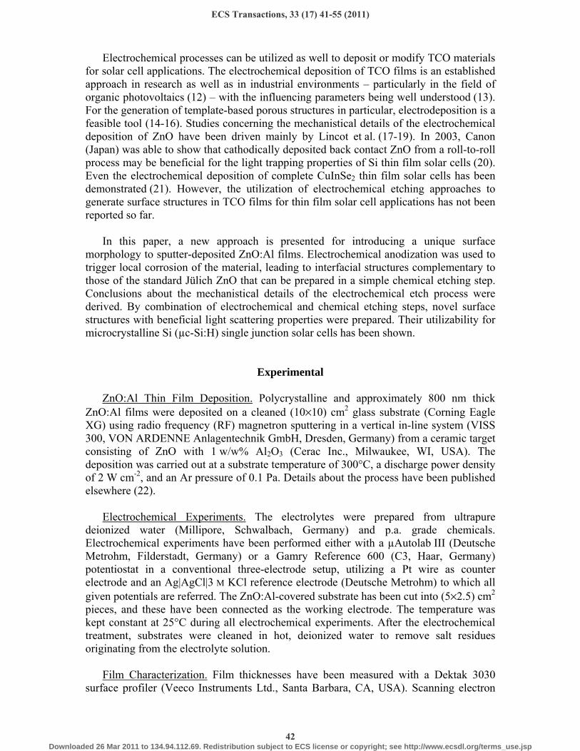
and the OER lead to a surface morphology not being significantly different from the as-deposited state (Fig. 2a). A slight change is observed solely at the grain boundaries that seem to deepen in the course of the experiment (Fig. 2b). Obviously, both interfacial reactions (Eqs. 1 and 2) are distinctly limited to the grain boundaries of the poly-crystalline material with a stunning degree of selectivity. This is an indication for direct lattice decomposition (34). The process is depicted in Fig. 3. Surface profilometric
ECS Transactions, 33 (17) 41-55 (2011)
44Downloaded 26 Mar 2011 to 134.94.112.69. Redistribution subject to ECS license or copyright; see http://www.ecsdl.org/terms_use.jsp
measurements support that observation as no integral thickness changes are observed after the electrochemical treatment. Even the electrochemically induced decrease in pH due to the OER has got a localized effect on the grain boundaries only and does not lead to a chemical dissolution of the c-axis oriented ZnO grains. This effect to the morphology of the substrate explains the previously mentioned breakdown of lateral conductivity at prolonged treatment times: Once the grain boundary pits reach the glass substrate, the sheet resistance will raise significantly.
H+
H O2 O2
e-ZnO
O2
e-
Zn +2
ZnO grains ZnO grains
Figure 3. Schematic illustration of the reactions occuring at the ZnO:Al/electrolyte interface during anodic biasing to potentials of O2 evolution.
The structure resulting from the electrochemical treatment is remarkable as it differs
significantly from the crater-like structures of the standard Jülich ZnO etched in diluted HCl only (3,4). Even though there are strong experimental indications for the grain boundaries – and especially the triple points of grain boundaries – being the origin of crater growth when etching with HCl (35), the grains are nevertheless etched as well. Craters extend over several grains during the etch process. Such a locally limited effect as from the electrochemical anodization that strongly depends on the material properties of the ZnO:Al thin film cannot be achieved by any other chemical surface treatment. The fact that only the grain boundaries are the electrochemically active sites, however, supports the assumption that they might be the origin of each etch pit, independent whether the treatment is an electrochemical or purely chemical one.
It is noteworthy that the composition of the electrolyte does not have a significant
influence on the morphology after the electrochemical treatment as long as its pH is kept in the neutral range. Several electrolyte salts, such as KCl, K2SO4, and KNO3, have been used for the process. The resulting structures are very similar in all cases. Slight changes are observed in the dissolution rates and resulting sheet resistances. The interpretation of these effects is a focus of current research.
ECS Transactions, 33 (17) 41-55 (2011)
45Downloaded 26 Mar 2011 to 134.94.112.69. Redistribution subject to ECS license or copyright; see http://www.ecsdl.org/terms_use.jsp
Combination of Etching Steps The surface structures resulting from the electrochemical treatment are interesting
from a mechanistical point of view, because they allow an insight into the structural prerequisites of the material for the etching process. However, the electrochemically induced roughness on the nanoscale does exhibit limitations concerning the light scattering capabilities due to the small size and high regularity. Furthermore, the changed morphology may affect the Si deposition process and the TCO/p-Si contact because the grain boundary pit quickly reaches high aspect ratios even after short polarization periods (33).
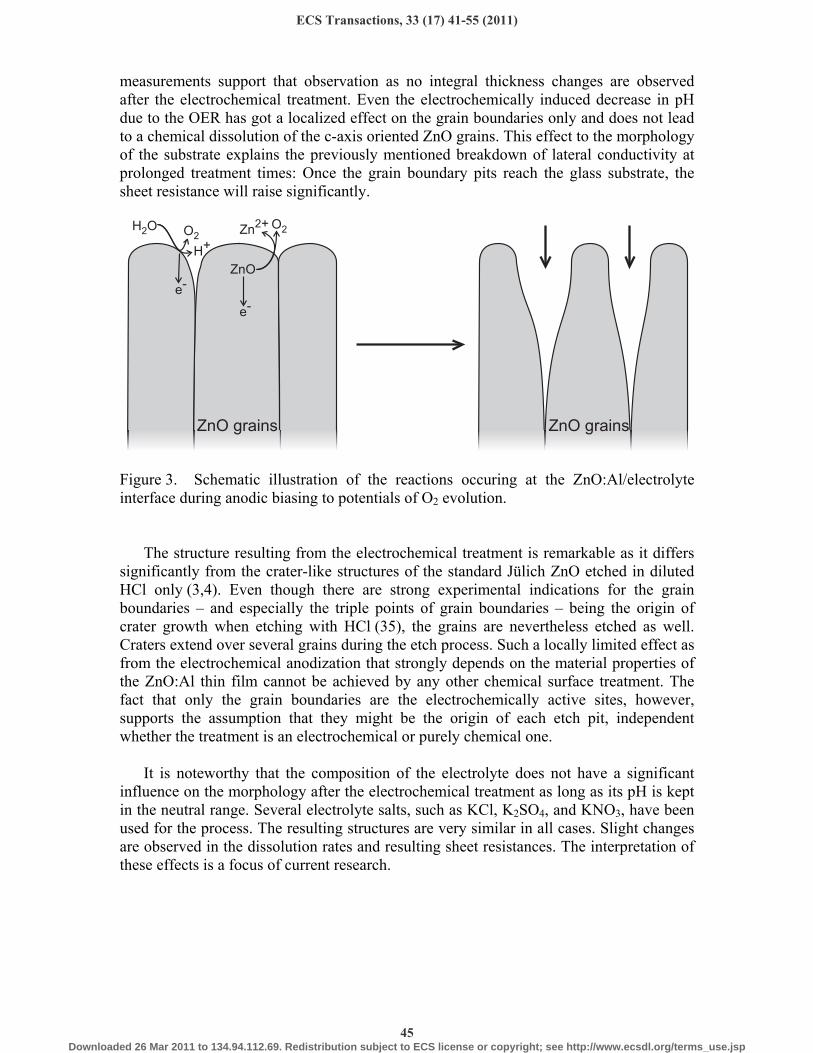
To generate surface structures being beneficial for light scattering purposes, it is a
logical choice to use the electrochemically treated substrates as templates for a subsequent chemical etching step. It was observed that this approach leads to a morphology that is similar to the standard Jülich ZnO, but with a higher crater density and, at the same time, lower crater diameter. Compared to the purely chemical treatment, etch pits are obviously not only generated at some peculiar grain boundaries. The electrochemical pretreatment seems to generate a significant number of new points of attack for the acidic etching. It widens the grain boundaries and thus possibly exposes new defect sites to the etchant. By changing the etch time in HCl, the morphology gradually shifts from extremely small craters to sizes being closer to those after a purely chemical etch (Fig. 4). This allows a quite selective tuning of the surface structure according to the needs of the Si absorber.
a) b) c)
500 nm
500 nm 500 nmd) e) f)
500 nm
500 nm
500 nm
Figure 4. SEM micrographs of ZnO:Al thin films after biasing at +2 V for 10 min in 0.1 M K2SO4 and subsequent etching in 0.5 w/w% HCl for a) a short dip, b) 5 s, c) 10 s, d) 20 s, e) 30 s, f) 40 s.
Generally speaking, the combination of electrochemical and chemical treatment
opens up ways to change the crater size on sputter-deposited ZnO thin films in the range
ECS Transactions, 33 (17) 41-55 (2011)
46Downloaded 26 Mar 2011 to 134.94.112.69. Redistribution subject to ECS license or copyright; see http://www.ecsdl.org/terms_use.jsp
between extremely narrow structures and the standard Jülich ZnO morphology. This aspect of this novel approach is extremely interesting because of two reasons:
(i) The size of the craters has got a significant influence on light scattering in
different regions of the spectrum of light. By selectively tuning the crater size, a material may be optimized for the needs of the Si absorber that is being deposited on top of it. This could, for example, allow a better adaption of a ZnO thin film sputtered at certain conditions to single junction and tandem solar cells.
(ii) Berginski et al. (22) reported that different sputtering conditions lead to ZnO thin films with different electrical and optical properties as well as different etching behaviors. This can result in films being excellent in terms of conductivity. However, etching in diluted HCl leads to craters with a diameter of > 1 µm and a low crater density. These structures do not lead to appropriate light scattering and are thus not desirable for an application in Si thin film solar cells. The novel approach reported herein could help to overcome this drawback: It could tune the surface structure of such electrically favorable ZnO films to improve their light scattering abilities. This is similar to the approach by Owen et al. (4) utilizing diluted HF as etchant.
Electrical Properties after Electrochemical and Chemical Treatment. Hall measure-
ments have been performed to determine the electrical properties of the textured ZnO:Al thin films shown in Fig. 4. Figure 5 shows the resistivity, carrier concentration, mobility, and sheet resistance as a function of etch time in 0.5 w/w% HCl.
The most obvious result of these measurements is the increase of sheet resistance as a
function of etch time, starting at (3.3±0.2) Ω□ in the as-deposited state (shown at 0 s) and increasing to (13.0±0.6) Ω□ after electrochemical pretreatment and 40 s of etching in diluted HCl. The latter value is significantly higher than those of the standard Jülich ZnO films that usually lie well below 10 Ω□. The reference substrate after chemical treatment (shown in grey) gives a value as low as (5.1±0.3) Ω□. A similar trend is observed for the resistivity. This steep increase in resistance for the twice-etched substrates indicates that the chemical etching step is accelerated by the electrochemical pretreatment. This supports the assumption that new points of attack for the etchant are generated by the anodization step. This observation, however, illustrates the necessity for a careful consideration between improved optical properties, originating from more optimized surface morphologies, and a lowered conductivity, which is of course not desirable for an application of these films in solar cells.
ECS Transactions, 33 (17) 41-55 (2011)
47Downloaded 26 Mar 2011 to 134.94.112.69. Redistribution subject to ECS license or copyright; see http://www.ecsdl.org/terms_use.jsp
Figure 5. Electrical properties of twice-etched, RF-sputtered ZnO:Al thin films derived from Hall measurements. All films were firstly biased at +2 V for 10 min in 0.1 M K2SO4 and secondly etched in 0.5 w/w% HCl for different etch times. The value at 0 s etch time shows the properties of the untreated, as-deposited film. The standard Jülich ZnO reference (ZnO:Al etched in 0.5 w/w% HCl for 40 s without electrochemical treatment) is shown in grey.
The mobility and carrier concentration are not influenced significantly by the electro-
chemical treatment; the values remain almost constant within the measurement un-certainty. Interestingly, the carrier concentration in the standard Jülich ZnO reference film etched for 40 s in HCl without electrochemical pretreatment is approximately 2.5×1020 cm-3 higher than that after anodization and etching in HCl for 40 s. However, this aspect should not be overinterpreted as the error in film thickness measurements has to be considered for the determination of the carrier concentration as well. This error clearly dominates the total measurement error on rough films. The same is true for the resistivity measurements.
Influence of the Electrolyte. As mentioned before, the composition of the electrolyte
is almost not affecting the surface morphology of the substrate after the electrochemical treatment as soon as neutral or slightly alkaline pH conditions are met. This is not true for the twice-etched ZnO thin films, though. While the craters on the surface of the ZnO film can be gradually widened after anodization in K2SO4 and remain below the size of the reference craters (Fig. 4), the resulting structures are markedly different when utilizing KCl as electrolyte in the electrochemical etch step (Fig. 6).
ECS Transactions, 33 (17) 41-55 (2011)
48Downloaded 26 Mar 2011 to 134.94.112.69. Redistribution subject to ECS license or copyright; see http://www.ecsdl.org/terms_use.jsp
a) b) c)
500 nm
500 nm 500 nm
d) e) f)
500 nm
500 nm
500 nm
Figure 6. SEM micrographs of ZnO:Al thin films after biasing at +2 V for 5 min in 0.1 M KCl and subsequent etching in 0.5 w/w% HCl for a) a short dip, b) 5 s, c) 10 s, d) 20 s, e) 30 s, f) 40 s.
With KCl as electrolyte, the influence of the electrochemical pretreatment seems to
be less pronounced. In the initial phase, e.g., after a short dip in HCl (Fig. 6a), the accentuation of the grain boundaries is still visible in terms of an increased density of craters. This vanishes almost totally after subsequent etch steps (Fig. 6b-d). After 30 or 40 s of etching (Fig. 6e-f), the morphology is similar to that of a standard Jülich ZnO substrate etched in HCl only. Furthermore, the increase in crater diameter is not as gradual as it has been seen after anodization in K2SO4 (Fig. 4), although it is still visible. Two effects are considered as possible reasons for the observed difference: (i) Sulfate ions may affect the pH by a very limited buffer effect, thus being relevant for the proton induced etching (Eq. 3) following the oxygen evolution (Eq. 2). (ii) A very recent study (36) has shown that the dissolution of the passive film formed on Zn is increased by sulfate ions which might affect the etching process itself or possible subsequent precipitation reactions.
Obviously, these effects become especially evident after the etch step in HCl. This
might be an indication for structural differences inside the etched grain boundaries after the electrochemical treatment. These differences are invisible in SEM measurements and do not affect the electric properties of the film. We are currently undertaking further microscopic experiments to better understand the effect of the electrolyte on the anodization process. This will be reported in the near future.
Besides from mechanistical aspects, however, the observation of the twice-etched
film morphologies depending on the electrolyte composition as well introduces another parameter for the adjustment of the surface structure. As mentioned before, this aspect might be beneficial for a fine tuning of ZnO thin films with respect to light scattering into the Si absorber.
ECS Transactions, 33 (17) 41-55 (2011)
49Downloaded 26 Mar 2011 to 134.94.112.69. Redistribution subject to ECS license or copyright; see http://www.ecsdl.org/terms_use.jsp
µc-Si:H Solar Cell Results. To check the quality of the twice-etched ZnO films in terms of light scattering ability and electrical contact to the p-doped layer of the Si absorber, (1×1) cm2 µc-Si:H single junction thin film solar cells have been prepared. A ~1 µm thick absorber with a ZnO/Ag back contact was used as layer system, utilizing the twice-etched ZnO:Al film as front contact. To evaluate the influence of the electrochemical pretreatment and the crater diameter, solar cell deposition was carried out on all films as shown in Fig. 6 and, in addition to that, on a standard Jülich ZnO reference substrate etched in 0.5 w/w% HCl for 50 s only. The characteristic parameters of these solar cells, namely the initial efficiency ηinit, fill factor FF, open circuit voltage Voc, and short circuit current density Jsc, are shown in Fig. 7 as a function of the etch time in 0.5 w/w% HCl. Please note that, other than in Fig. 5, the data set at 0 s etch time does not represent the as-deposited ZnO:Al thin film, but the film after anodization without any etch step in HCl.
Figure 7. Initial efficiency ηinit, fill factor FF, open circuit voltage Voc, and short circuit current density Jsc of µc-Si:H solar cells on twice-etched, RF-sputtered ZnO:Al films. All films were firstly biased at +2 V for 5 min in 0.1 M KCl and secondly etched in 0.5 w/w% HCl for different etch times before Si deposition. The data set marked as HCl reference (solar cell with standard Jülich ZnO:Al etched in 0.5 w/w% HCl for 50 s without electrochemical treatment) is shown in grey.
The most obvious outcome of this experiment is the fact that ηinit as well as Jsc
increase as a function of the etch time in HCl. As the craters grow in diameter and in depth, the light scattering ability of the ZnO:Al thin film is enhanced. This increases the
ECS Transactions, 33 (17) 41-55 (2011)
50Downloaded 26 Mar 2011 to 134.94.112.69. Redistribution subject to ECS license or copyright; see http://www.ecsdl.org/terms_use.jsp
probability of light absorption in the Si absorber due to a prolongation of the optical path length and due to improved light trapping (1). Thus, the current increases. In this experiment, the highest current density values are in the range of (23.2±0.1) mA cm-2 for the twice-etched films. This corresponds well to Jsc of the standard Jülich ZnO reference film, but does not exceed it. That is consistent with the observation that the morphology of the film (Fig. 6f) is very similar to that of the reference with crater diameters in the range of a few 100 nm.
a) b)
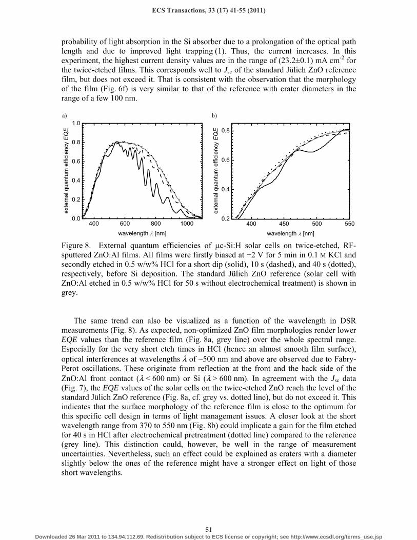
Figure 8. External quantum efficiencies of µc-Si:H solar cells on twice-etched, RF-sputtered ZnO:Al films. All films were firstly biased at +2 V for 5 min in 0.1 M KCl and secondly etched in 0.5 w/w% HCl for a short dip (solid), 10 s (dashed), and 40 s (dotted), respectively, before Si deposition. The standard Jülich ZnO reference (solar cell with ZnO:Al etched in 0.5 w/w% HCl for 50 s without electrochemical treatment) is shown in grey.
The same trend can also be visualized as a function of the wavelength in DSR
measurements (Fig. 8). As expected, non-optimized ZnO film morphologies render lower EQE values than the reference film (Fig. 8a, grey line) over the whole spectral range. Especially for the very short etch times in HCl (hence an almost smooth film surface), optical interferences at wavelengths λ of ~500 nm and above are observed due to Fabry-Perot oscillations. These originate from reflection at the front and the back side of the ZnO:Al front contact (λ < 600 nm) or Si (λ > 600 nm). In agreement with the Jsc data (Fig. 7), the EQE values of the solar cells on the twice-etched ZnO reach the level of the standard Jülich ZnO reference (Fig. 8a, cf. grey vs. dotted line), but do not exceed it. This indicates that the surface morphology of the reference film is close to the optimum for this specific cell design in terms of light management issues. A closer look at the short wavelength range from 370 to 550 nm (Fig. 8b) could implicate a gain for the film etched for 40 s in HCl after electrochemical pretreatment (dotted line) compared to the reference (grey line). This distinction could, however, be well in the range of measurement uncertainties. Nevertheless, such an effect could be explained as craters with a diameter slightly below the ones of the reference might have a stronger effect on light of those short wavelengths.
ECS Transactions, 33 (17) 41-55 (2011)
51Downloaded 26 Mar 2011 to 134.94.112.69. Redistribution subject to ECS license or copyright; see http://www.ecsdl.org/terms_use.jsp
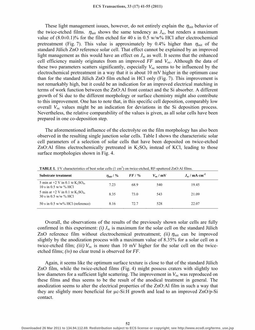
These light management issues, however, do not entirely explain the ηinit behavior of the twice-etched films. ηinit shows the same tendency as Jsc, but renders a maximum value of (8.0±0.1)% for the film etched for 40 s in 0.5 w/w% HCl after electrochemical pretreatment (Fig. 7). This value is approximately by 0.4% higher than ηinit of the standard Jülich ZnO reference solar cell. That effect cannot be explained by an improved light management as this would have an effect on Jsc as well. It seems that the enhanced cell efficiency mainly originates from an improved FF and Voc. Although the data of these two parameters scatters significantly, especially Voc seems to be influenced by the electrochemical pretreatment in a way that it is about 10 mV higher in the optimum case than for the standard Jülich ZnO film etched in HCl only (Fig. 7). This improvement is not remarkably high, but it could be an indication for an improved electrical matching in terms of work function between the ZnO:Al front contact and the Si absorber. A different growth of Si due to the different morphology or surface chemistry might also contribute to this improvement. One has to note that, in this specific cell deposition, comparably low overall Voc values might be an indication for deviations in the Si deposition process. Nevertheless, the relative comparability of the values is given, as all solar cells have been prepared in one co-deposition step.
The aforementioned influence of the electrolyte on the film morphology has also been
observed in the resulting single junction solar cells. Table I shows the characteristic solar cell parameters of a selection of solar cells that have been deposited on twice-etched ZnO:Al films electrochemically pretreated in K2SO4 instead of KCl, leading to those surface morphologies shown in Fig. 4.
TABLE I. I/V characteristics of best solar cells (1 cm2) on twice-etched, RF-sputtered ZnO:Al films.
5 min at +2 V in 0.1 M K2SO4, 10 s in 0.5 w/w % HCl 7.23 68.9 540 19.45
5 min at +2 V in 0.1 M K2SO4, 30 s in 0.5 w/w % HCl 8.35 73.0 543 21.09
50 s in 0.5 w/w% HCl (reference) 8.16 72.7 528 22.07
Overall, the observations of the results of the previously shown solar cells are fully
confirmed in this experiment: (i) Jsc is maximum for the solar cell on the standard Jülich ZnO reference film without electrochemical pretreatment; (ii) ηinit can be improved slightly by the anodization process with a maximum value of 8.35% for a solar cell on a twice-etched film; (iii) Voc is more than 10 mV higher for the solar cell on the twice-etched films; (iv) no clear trend is observed for FF.
Again, it seems like the optimum surface texture is close to that of the standard Jülich
ZnO film, while the twice-etched films (Fig. 4) might possess craters with slightly too low diameters for a sufficient light scattering. The improvement in Voc was reproduced on these films and thus seems to be the result of the anodical treatment in general. The anodization seems to alter the electrical properties of the ZnO:Al film in such a way that they are slightly more beneficial for µc-Si:H growth and lead to an improved ZnO/p-Si contact.
ECS Transactions, 33 (17) 41-55 (2011)
52Downloaded 26 Mar 2011 to 134.94.112.69. Redistribution subject to ECS license or copyright; see http://www.ecsdl.org/terms_use.jsp
Conclusions In summary, we have presented a novel approach to change the surface morphology
of RF-sputtered ZnO:Al thin films by means of an anodic electrochemical treatment. The resulting interfacial reaction is distinctly limited to the grain boundaries of the thin film, leading to unique surface structures that cannot be achieved by any other solution-based technique. The combination of this electrochemical approach with chemical etching in diluted HCl allowed us to tune the surface morphology of the ZnO:Al thin films such that it might be beneficial for an application as a front contact in Si thin film solar cells. Aditionally, the electrochemical treatment seems to advantageously influence the electrical properties of the ZnO for subsequent Si deposition.
The application of such films in µc-Si:H single junction solar cells has proven their
utilizability for Si thin film photovoltaic applications. It was observed that the tuning of the ZnO film surface morphology might lead to an improved light management in the solar cell. The generation of optimum structures, though, strongly depends on the experimental parameters of the surface treatment (electrochemical as well as chemical) and on the physical properties of the ZnO film.
While the results reported in this paper are only the initial step towards an
optimization of the etching procedure, the potential of the electrochemical treatment for an improvement of sputter-deposited ZnO front contact layers has been clearly demonstrated. Further work has to be done to understand and systemize the influence of the electrochemical treatment on the ZnO thin film and on the resulting solar cells. Such experiments are currently under way. Especially for such films with excellent electrical and optical properties derived from slightly different deposition conditions that cannot be etched easily in the established processes, the electrochemical treatment might be the key for an application as front contacts in Si thin film solar cells. This might ultimately lead to an increased overall solar cell performance. Furthermore, a better insight into the mechanisms of the electrochemical etch process will contribute significantly to an in-depth understanding of the etching of sputter-deposited ZnO thin films in general.
Acknowledgments
The authors thank Carsten Grates, Joachim Kirchhoff, and Etienne Moulin for assistance in solar cell preparation and characterization as well as Jan-Philipp Becker, Aad Gordijn and Uwe Rau (all Forschungszentrum Jülich GmbH) for fruitful discussions. SEM images have been recorded by Hans Peter Bochem (IBN-PT, Forschungszentrum Jülich GmbH). Financial support by the German Federal Environment Ministry (BMU, grant 0327693A), Dortmunder Oberflächencentrum, and by the Deutsche Forschungs-gemeinschaft (DFG, grant PU 447/1-1) is gratefully acknowledged.
References
1. J. Hüpkes, J. Müller, and B. Rech, in Transparent Conductive Zinc Oxide: Basics and Applications in Thin Film Solar Cells, K. Ellmer, A. Klein, and B. Rech, Editors, p. 362, Springer, Berlin, Germany (2008).
ECS Transactions, 33 (17) 41-55 (2011)
53Downloaded 26 Mar 2011 to 134.94.112.69. Redistribution subject to ECS license or copyright; see http://www.ecsdl.org/terms_use.jsp
2. B. Rech and H. Wagner, Appl. Phys. A, 69, 155 (1999). 3. M. Kubon, E. Boehmer, F. Siebke, B. Rech, C. Beneking, and H. Wagner, Sol.
Energy Mater. Sol. Cells, 41-42, 485 (1996). 4. J. I. Owen, J. Hüpkes, H. Zhu, E. Bunte, and S. E. Pust, Phys. Status Solidi A, doi:
10.1002/pssa.201026164 (in press). 5. J. I. Owen, J. Hüpkes, E. Bunte, S. E. Pust, and A. Gordijn, in Proceedings of the
25th European Photovoltaic Solar Energy Conference, Valencia, Spain, pp. 2951-2955, WIP, Munich, Germany (2010).
6. J. Hüpkes, J. I. Owen, E. Bunte, H. Zhu, S. E. Pust, J. Worbs, and G. Jost, in Proceedings of the 25th European Photovoltaic Solar Energy Conference, Valencia, Spain, pp. 3224-3227, WIP, Munich, Germany (2010).
7. J. W. Kwon and E. S. Kim, J. Microelectromech. Syst., 14, 603 (2005). 8. S. Fernández, A. Bollero, F. B. Naranjo, O. de Abril, J. Cárabe, and J. J. Gandía,
Proceedings of the 25th European Photovoltaic Solar Energy Conference, Valencia, Spain, pp. 2991-2995, WIP, Munich, Germany (2010).
9. A. N. Mariano and R. E. Hanneman, J. Appl. Phys., 34, 384 (1963). 10. W. Jo, S.-J. Kim, and D.-Y. Kim, Acta Mater., 53, 4185 (2005). 11. H. C. Gatos, J. Appl. Phys., 32, 1232 (1961). 12. Q. Zhang, C. S. Dandeneau, X. Zhou, and G. Cao, Adv. Mater. (Weinheim, Ger.),
21, 4087 (2009). 13. T. Yoshida, J. Zhang, D. Komatsu, S. Sawatani, H. Minoura, T. Pauporté, D.
Lincot, T. Oekermann, D. Schlettwein, H. Tada, D. Wöhrle, K. Funabiki, M. Matsui, H. Miura, and H. Yanagi, Adv. Funct. Mater., 19, 17 (2009).
14. H. Yan, Y. Yang, Z. Fu, B. Yang, L. Xia, S. Fu, and F. Li, Electrochem. Commun., 7, 1117 (2005).
15. Z. Liu, Z. Jin, X. Liu, W. Wu, and W. Li, Semicond. Sci. Technol., 21, 60 (2006). 16. J. Elias, C. Lévy-Clément, M. Bechelany, J. Michler, G.-Y. Wang, Z. Wang, and
L. Philippe, Adv. Mater. (Weinheim, Ger.), 22, 1607 (2010). 17. S. Peulon and D. Lincot, J. Electrochem. Soc., 145, 864 (1998). 18. B. Canava and D. Lincot, J. Appl. Electrochem., 30, 711 (2000). 19. A. Goux, T. Pauporte, J. Chivot, and D. Lincot, Electrochim. Acta, 50, 2239
(2005). 20. N. Toyama, R. Hayashi, Y. Sonoda, M. Iwata, Y. Miyamoto, H. Otoshi, K. Saito,
and K. Ogawa, Proceedings of 3rd World Conference on Photovoltaic Energy Conversion, 2, 1601 (2003).
21. R. P. Raffaelle, W. Junek, J. Gorse, T. Thompson, J. D. Harris, J. Cowen, D. Hehemann, G. Rybicki, and A. F. Hepp, Mater. Res. Soc. Symp. Proc., 606, 155 (2000).
22. M. Berginski, J. Hüpkes, M. Schulte, G. Schöpe, H. Stiebig, B. Rech, and M. Wuttig, J. Appl. Phys., 101, 074903 (1990).
23. T. Roschek, T. Repmann, J. Müller, B. Rech, and H. Wagner, J. Vac. Sci. Technol., 20, 492 (2002).
24. B. Rech, T. Roschek, T. Repmann, J. Müller, R. Schmitz, and W. Appenzeller, Thin Solid Films, 427, 157 (2003).
25. O. Fruhwirth, G. W. Herzog, and J. Poulios, Surf. Technol., 24, 293 (1985). 26. H. Gerischer and N. Sorg, Mater. Corros., 42, 149 (1991). 27. J. Hüpkes, B. Rech, S. Calnan, O. Kluth, U. Zastrow, H. Siekmann, and M.
Wuttig, Thin Solid Films, 502, 286 (2006). 28. Y. C. Lin, Y. C. Jian, and J. H. Jiang, Appl. Surf. Sci., 254, 2671 (2008).
ECS Transactions, 33 (17) 41-55 (2011)
54Downloaded 26 Mar 2011 to 134.94.112.69. Redistribution subject to ECS license or copyright; see http://www.ecsdl.org/terms_use.jsp
29. M. Pourbaix, Atlas of Electrochemical Equilibria in Aqueous Solutions, p. 411, National Association of Corrosion Engineers, Houston, TX, USA (1974).
30. M. Valtiner, S. Borodin, and G. Grundmeier, Langmuir, 24, 5350 (2008). 31. H. Gerischer and N. Sorg, Electrochim. Acta, 37, 827 (1992). 32. Z. Zembura and L. Burzynska, Corros. Sci., 17, 871 (1977). 33. S. O. Klemm, S. E. Pust, A. W. Hassel, J. Hüpkes, and K. J. J. Mayrhofer, J. Solid
State Electrochem., submitted for publication. 34. H. L. Tuller, J. Electroceram., 4, 33 (1999). 35. J. I. Owen, J. Hüpkes, and E. Bunte, Mater. Res. Soc. Symp. Proc., 1153, A07-08
(2009). 36. S. O. Klemm, J.-C. Schauer, B. Schuhmacher, and A. W. Hassel, Electrochim.
Acta, submitted for publication.
ECS Transactions, 33 (17) 41-55 (2011)
55Downloaded 26 Mar 2011 to 134.94.112.69. Redistribution subject to ECS license or copyright; see http://www.ecsdl.org/terms_use.jsp


![Structural and Electrochemical Investigation of Zinc-Doped ... · electrochemical energy storage systems [10, 11]. As a layered n-type semiconductor, MoO 3 has been put into practice](https://static.documents.pub/doc/80x56/6061bf27ca9f7b579b04fd93/structural-and-electrochemical-investigation-of-zinc-doped-electrochemical-energy.jpg)


