Electrocomponent Science and Technology 1976, Vol. 3, pp. 103-111 (C) Gordon and Breach Science Publishers Ltd., 1976 Printed in Great Britain ELECTROLESS PLATING ITS APPLICATIONS IN RESISTOR TECHNOLOGY J. DEARDEN Welwyn Electric Ltd., Bedlington, Northumberland, U.K. (Received January 8, 1976; in final form May 12, 1976) Electroless processes for the deposition of metal films onto insulators have been known for many years. Various aspects of this technology have been applied in the field of resistor technology leading to improved performance of existing resistors and the evaluation of new resistors with novel characteristics. The applications of electroless nickel as a readily solderable, completely ohmic contact for tin oxide resistors is described. Copper oxide layers produced from oxidised electroless copper are shown to improve the thermal stability of tin oxide resistors. A range of electroless high precision metal film resistors from a fraction of an ohm to 100 kohm per square and from a few millimetres in length to over metre is shown to be feasible. This technology has been applied to the manufacture of thin film circuits. The outstanding thermal stability of the electroless nickel-boron films and their temperature coefficient of resistance indicates a potential application in the field of temperature sensors. The ability to produce "weightless" films on Mylar sheet at 10 Gohm per square is considered to be a solution to the charge distribution requirement for electrostatic loudspeakers. INTRODUCTION With the rapid growth in the knowledge of electroless plating techniques over the past 30 years it was inevitable that it should attract the attention of technologists working with thin film electronic components. One of its main attractions was the fact that metal films could be deposited onto non-conductors under low temperature conditions and in very mild solution ambients. In addition the outlay on equipment to deposit these films constituted no more than the cost of simple everyday laboratory items. This paper summarises some of the pertinent literature and describes some of the uses of electroless plating in resistor technology, indicating why it was contemplated at the particular time and in some cases how it gave a successful answer to the problem. 2 LITERATURE SUMMARY The electroless deposition of metals is usually carried out by reduction in an aqueous solution of a metal salt either by an organic or an inorganic reducing agent dissolved in the solution. The reduction process requires the presence of catalytic nuclei before it can take place effectively. Silver was the first metal to be deposited in film form, to replace the rather dangerous silver-mercury amalgam previously used in the manufacture of mirrors. In 1826 Von Liebig found that by heating acetaldehyde with an ammoniacal solution of silver nitrate in a glass vessel a brilliant silver mirror formed on the surface of the glass. A search of the technical and patent literature on silvering processes discloses a vast number of papers on the subject in a wide variety of languages. Most of the quoted processes involved the pre-treatment of the surface to be silvered with a dilute solution of stannous chloride, which provided catalytically active centres to promote silver deposition. The plating solutions used are numerous and a selection of these can be found in a summary article by Wein. 1 Like silver, copper films can be deposited onto non-conductors by a similar chemical route. However, in order to promote the deposition it is usually necessary to have a trace of a precious metal salt in the metallising solution. In another article Wein 2 describes some of the more successful electroless copper solutions. The deposition of nickel and its alloys has attracted much attention during the past thirty years due mainly to the chemical inertness of the films and their interesting electrical and magnetic properties. As with silver and copper, the films are formed by 103
Transcript
Electrocomponent Science and Technology1976, Vol. 3, pp. 103-111
(C) Gordon and Breach Science Publishers Ltd., 1976Printed in Great Britain
ELECTROLESS PLATING ITS APPLICATIONS INRESISTOR TECHNOLOGY
J. DEARDEN
Welwyn Electric Ltd., Bedlington, Northumberland, U.K.
(Received January 8, 1976; in final form May 12, 1976)
Electroless processes for the deposition of metal films onto insulators have been known for many years. Variousaspects of this technology have been applied in the field of resistor technology leading to improved performanceof existing resistors and the evaluation of new resistors with novel characteristics.
The applications of electroless nickel as a readily solderable, completely ohmic contact for tin oxide resistors isdescribed.
Copper oxide layers produced from oxidised electroless copper are shown to improve the thermal stability of tinoxide resistors.
A range of electroless high precision metal film resistors from a fraction of an ohm to 100 kohm per square andfrom a few millimetres in length to over metre is shown to be feasible. This technology has been applied to themanufacture of thin film circuits.
The outstanding thermal stability of the electroless nickel-boron films and their temperature coefficient ofresistance indicates a potential application in the field of temperature sensors.
The ability to produce "weightless" films on Mylar sheet at 10 Gohm per square is considered to be a solution tothe charge distribution requirement for electrostatic loudspeakers.
INTRODUCTION
With the rapid growth in the knowledge of electrolessplating techniques over the past 30 years it wasinevitable that it should attract the attention oftechnologists working with thin film electroniccomponents.
One of its main attractions was the fact that metalfilms could be deposited onto non-conductors underlow temperature conditions and in very mild solutionambients. In addition the outlay on equipment todeposit these films constituted no more than the costof simple everyday laboratory items.
This paper summarises some of the pertinentliterature and describes some of the uses of electrolessplating in resistor technology, indicating why it wascontemplated at the particular time and in some caseshow it gave a successful answer to the problem.
2 LITERATURE SUMMARY
The electroless deposition of metals is usually carriedout by reduction in an aqueous solution of a metalsalt either by an organic or an inorganic reducing agentdissolved in the solution. The reduction processrequires the presence of catalytic nuclei before it cantake place effectively.
Silver was the first metal to be deposited in filmform, to replace the rather dangerous silver-mercuryamalgam previously used in the manufacture ofmirrors. In 1826 Von Liebig found that by heatingacetaldehyde with an ammoniacal solution of silvernitrate in a glass vessel a brilliant silver mirrorformed on the surface of the glass.A search of the technical and patent literature on
silvering processes discloses a vast number of paperson the subject in a wide variety of languages. Most ofthe quoted processes involved the pre-treatment ofthe surface to be silvered with a dilute solution ofstannous chloride, which provided catalytically activecentres to promote silver deposition. The platingsolutions used are numerous and a selection of thesecan be found in a summary article by Wein. 1
Like silver, copper films can be deposited ontonon-conductors by a similar chemical route. However,in order to promote the deposition it is usuallynecessary to have a trace of a precious metal salt inthe metallising solution. In another article Wein2
describes some of the more successful electrolesscopper solutions.
The deposition of nickel and its alloys hasattracted much attention during the past thirty yearsdue mainly to the chemical inertness of the films andtheir interesting electrical and magnetic properties.
As with silver and copper, the films are formed by
103
104 J. DEARDEN
reduction of solutions of nickel salts. A nickel-phosphorus "alloy" can be deposited using sodiumhypophosphite as the reducing agent. The reactionwas first observed by Wurtz3 in 1844; it was, however,a spontaneous uncontrolled reaction which producedonly a black powder.
It was not until 1947 that Brenner and Riddell4 atthe American National Bureau of Standards demon-strated that a stable and controllable plating processwas possible onto certain chemically active metallicsurfaces. They also showed that once the reaction hadbeen started it was autocatalytic thus allowing thickdeposits to be formed, a feature which was absent inthe silver and copper reactions, both of these pro-cesses being self limiting.
Depositions onto non-metallic surfaces did notmeet with much success until Brenner reported on amethod of sensitising insulating surfaces by rinsingin stannous chloride solution followed by a rinse in adilute palladium chloride solution. This deposited amonoatomic layer of a palladium-tin complex on theinsulating surface which in turn was highly catalytictowards the hypophosphite reduction of the nickelsolution.
Gutzeit6 showed that the phosphorus content ofthese films could be varied between 7 and 15 per centby changing the pH of the plating solution.
Because of the brittle nature of the nickel phos-phorus film several attempts were made to findalternative reducing agents. Dini and Coronado7 weresuccessful in producing almost pure nickel films byusing hydrazine instead of sodium hypophosphite.After suitable heat treatment these deposits wereshown to be highly ductile and possess interestingmagnetic properties i.e. low coercivity, high satura-tion magnetisation and hysteresis loops with highsquareness ratios.
Other classes of reductants for electroless nickelplating which have received a considerable amount ofattention are the borohydrides and boranes. Theseproduce nickel films with up to 7 per cent boron, andNarcus,8 in a useful summary paper, claims thatthese processes, because of their low temperatureoperation, are particularly useful for applying con-ductive metal films to temperature sensitive thermo-plastics. He also claims that after heat treatment onrefractory substrates, nickel boride is formed in thefilm endowing it with a high degree of abrasionresistance and chemical inertness.
It can be seen from this brief survey on a widelysubscribed topic that anyone who is working in thefield of thin film components could not help resorting,at some time, to its information for solutions to prob-
lems or as a basis for a new component. A usefulreference book by Goldie 14 on the general topic ofelectroless deposition of metal f’rims is now available.
3 ELECTRICAL CONTACT CONSIDERATIONSFOR TIN OXIDE FILM RESISTORS
Shortly after the introduction of the tin oxide filmresistor a need arose to dispense with the thenrather bulky turned brass caps used for the endcontacts.
The obvious answer was to produce a resistor withmetal film contact bands with lead wires soldereddirectly to the metal film. The proposed design isshown in Figure 1.
Leod wire. Metal Tin ide Solder() contact coated ceramic fi Itet.band. rod. ( ()
FIGURE Capless Resistor Design
The tin oxide coated ceramic rod (1)had "blind"holes at each end into which the tinned copper leadwires (2) could be inserted and subsequentlysoldered (3) onto the metal contact bands (4)(numbers refer to Figure 1). If this type of construc-tion could be achieved then it would eliminate theuse of the costly brass caps and provide a smoothprojectionless outline to the resistor.
The key to the success of this design was theprovision of a satisfactory metal contact whichwould:
a) Give a good electrical contact to the tin oxidefilm
b) Have adequate adherence
c) Solder easily
Both electroless silver and copper films were triedand both gave excellent electrical contacts butsoldering difficulties were encountered due to theirhigh level of solubility in molten solder aggravatedby their thinness and open pore structure.
As an alternative, "fired on" thick film silvercontact bands were investigated. These gave excellentadherence and were readily soldered using soldercontaining a small percentage of silver. However, theelectrical quality of the contact was poor due to a
ELECTROLESS PLATING 105
high resistivity tin oxide layer which formed at theinterface between the silver and the resistive filmduring the firing on of the contact bands at atemperature around 500C.
It was clear that copper and in particular silverwere not offering a solution to this particularcontact problem. However, at this time the Brennerprocess was becoming widely known for thedeposition of nickel-phosphorus films onto non-conductors.
This process seemed to have much to offerbecause, like the electroless silver process, the filmswere deposited under low temperature reducingconditions and in addition the reaction was selfcatalytic, thus holding out the possibility of pro-ducing thick films less likely to give solderingproblems.
The usefulness of this approach was subsequentlyproven and it gave the required quality of electricalcontact, adequate adherence, and, most important ofall, problem-free soldering with no leaching of themetal contact by the solder.A bonus which came to light during the early
experiments was that the tin oxide resistive film had asufficiently high content of lower valency tin atomsthat it could itself initiate the deposition of thenickel-phosphorus film.9 This constrained the metaldeposition to the exposed tin oxide end bands and nometal deposition occurred on the centre maskinglacquer, thus allowing its easy removal with theappropriate solvent.
Using this electroless nickel method for applyingcontacts onto tin oxide resistors a successfulautomatic process was evolved to produce resistorsaccording to the design shown in Figure 1. With thisdesign the ultimate requirement for a smooth,conformal outline resistor was achieved.
4 IMPROVING THE ELECTRICAL STABILITYOF TIN OXIDE RESISTORS
Tin oxide resistive films by the very nature of theirformation, ice. high temperature hydrolysis of "doped"stannic chloride vapour, o depend for their conduc-tion on a degree of oxygen deficiency.
Under normal use these films have a high degree ofelectrical stability. There are certain extremeconditions, however, either during manufacture or inuse, in which the resistive film can encounter mildreducing effects leading to an increase in the level ofoxygen deficiency and hence a lowering of theresistivity of the tin oxide film.
To avoid such damage occurring, some thoughtwas given to the possibility of interposing a sourceof oxygen between the tin-oxide and its surroundings.A wide range of chemical oxygen sources wasexamined ranging from chromates and peroxides to abroad spectrum of elemental oxides.
The ideal solution was ultimately discovered incupric oxide, the optimum protection being givenwhen this material was formed as a layer in intimatecontact with the tin oxide film.A cheap and convenient method of forming this
cupric oxide layer was found using electroless platingtechniques.
() / Copper Copper plating.Tin oide oxa ()
coated ceramicrod. ()
FIGURE 2 Construction of Tin Oxide Resistor withimproved electrical stability
In Figure 2 the tin-oxide coated ceramic rod (1)was copper plated by one of the established electro-less plating methods. After plating, steel caps (2)were pressed onto the ends of the resistor over thecopper plating (3) thus ensuring perfect electricalcontact to the tin oxide film. The exposed copperfilm between the caps was then fully oxidised (4)by heating for 3 hours at 300 C. This caused nodamage to the tin oxide film but provided a highresistivity compact oxide barrier layer.
After the formation of the copper oxide layer theresistor was brought up to value by the cutting of ahelical groove through the copper oxide and tin oxide.The tinned copper lead wires were then welded ontothe caps and the appropriate organic lacquer pro-tection applied.
The presence of the copper oxide kept the pro-cessing changes to a fraction of their value before theuse of this protective layer, thus enabling closertolerance resistors to be produced.
5 NEW COMPONENTS
5.1 Metal Film Resistors
The ability to deposit metal films onto ceramicsurfaces by simple and inexpensive techniques was an
106 J. DEARDEN
obvious invitation to examine their electricalproperties.
In 1959 a comprehensive investigation programmewas started to study the nickel/phosphorus andcobalt/phosphorus electroless films to see if they werecapable of yielding useful resistor properties. Thefilms were deposited by the then classical method ofactivating the ceramic surface by treatment withstannous chloride/palladium chloride followed bydeposition of the film from a buffered nickel and/orcobalt salt solution using sodium hypophosphite asthe reducing agent.
The investigations were far-reaching and coveredall aspects of the process. Detailed electron micro-scopy studies were made of the activation stage andthe early stages of film formation in order to establishthe optimum conditions to achieve a high degree offilm uniformity; an important requirement forresistive t’rims.
Methods of varying the composition of the filmswere examined and the subsequent effect of this onthe film resistivity and temperature coefficient ofresistance (T.C.R.) was determined.
For any resistive film to be useful as a resistor itmust be electrically stable at elevated temperatureswhether these be determined by the ambienttemperature or by the electrical power beingdissipated by the resistor. It was necessary toestablish techniques to induce this stability because,as deposited, the films were shown to be highlyunstable both thermally and in moist ambientconditions.
It became evident that by varying the compositionand pH of the electroless nickel plating bath thephosphorus content of the deposited film could beaccurately controlled. This change in film compo-sition manifested itself as a change in resistivity of thealloy and hence in the surface resistivity of the filmitself. One of the interesting features was that arelatively large change in resistivity resulted in only asmall change in T.C.R.
By combining this effect with a variation of filmthickness it was possible to produce a range of surfaceresistivities from less than ohm per square to500 kohm per square with T.C.R.’s within+100 ppM/C.
The actual relationship between Film thickness,composition and surface resistivity is shown inFigure 3. In Figure 4 the results of 400 T.C.R.measurements 2 taken from production controlrecords are plotted against their correspondingsurface resistivities. They indicate a mean T.C.R. of+4 ppM/C with a standard deviation of 24 ppM/ C.
FIGURE 3 Relationship between film thickness,composition and surface resistivity for electroless nickel-phosphorus films
/100
/80
/60
/40
20
o-20
-40 ";--’
a -60,- -80
-100
10fl 100fl D 10DSheet Resistance (D per sq.)
FIGURE 4 The temperature coefficient of typicalbatches of metal film resistors of various sheet resistivities
It is interesting to note that the metal filmresistors marketed by other companies use evaporatednickel-chromium which in itself gives equally goodresistor performance but produces only a narrowrange of resistivities i.e. 10 ohm per square to justover kohm per square.
The excellent electrical stability of the electrolessnickel-phosphorus film is obtained by heating forseveral hours at an elevated temperature. Thiscompletes any Iatent chemical reactivity within thefilm and promotes the formation of the inertcompound nickel phosphides.
In order to ensure freedom from attack bymoisture the film is chemically treated to give it anouter passivated layer.
The number of resistor blanks or prevalues whichcan be produced per batch is limited only by thesize of the vessels in which they are plated. It alsofollows that the maximum size of the resistor isdictated only by the size of the vessel.
Resistors are produced from a few millimetres in
ELECTROLESS PLATING 107
FIGURE 5 Electroless nickel-phosphorus metal film resistors
length to well over metre. Examples are shown inFigure 5.
To give the resistors protection from mechanicaldamage and an extra barrier against hostile environ-ments they are finally coated with an organic lacquercontaining an epoxy resin This also provides thenecessary electrical insulation.
Since this process was introduced, very largenumbers of high quality precision resistors have beensold to the U.K. and foreign mar,kets and it is believedthat it is the only commercial electroless process in
the world producing metal film resistors in such largenumbers over such a wide range of values and sizes.
5.2 Integrated Orcuits
Shortly after the introduction of these metal filmresistors it became evident that there was a lobbywithin the electronics industry which cast doubt onthe reliability of circuits constructed from wire anddiscrete components, mainly due to failure at thesoldered joints.
108 J. DEARDEN
The so-called integrated circuit was seen as ananswer to these doubts. This concept involved thesimultaneous deposition of resistors onto a flatceramic substrate followed by conductors. This gavea continuous circuit intimately bonded over itsentirety to the substrate.
Once again the use of electroless plating processesappeared to offer a simple and effective solution.
The process adopted was based essentially on aceramic substrate although circuits were alsoproduced in limited quantities on glass epoxylaminate. The build-up of the circuit on the substratetook the following route :-
The substrate was chemically cleaned, activatedand coated all over with the electroless nickel-phosphorus resistive layer. This layer was stabilised
and passivated by subjecting it to the appropriatethermal and chemical treatments.
Using a screen printed lacquer mask or photo-resisttechnique, the resistive layer was fully protectedexcept where the conductor limbs would berequired these parts were left exposed. Theconductor limbs were reinforced with a heavy depositof low resistivity, low phosphorus content, electrolessnickel.
The lacquer mask was removed and by similarscreen printing or photoresist techniques theconductor areas were protected and a mask formed ofthe resistor pattern. The exposed resistive nickel wasetched away and the lacquer layer removed.
This produced the required reliable array ofresistors and conductors, examples of which are shown
FIGURE 6 Electroless nickel-phosphorus metal film integrated circuits
ELECTROLESS PLATING 109
in Figure 6. The discrete components, i.e. capacitorsand active devices, were soldered directly onto theappropriate termincal pads.
Terminal wires were securely attached throughholes in the substrate and the unit was protected withlacquer and potted in a moulded plastic box using oneof the many standard potting resins.
This thin film integrated circuit was in productionfrom 1962 to 1970 and during this time about aquarter of a million modules were sold.
The process was eventually superseded by thescreen printed thick film technique due mainly to thefact that it was a cheaper process and the propertiesof the thick film resistors were as good as, and insome respects, better than the thin film resistors.
5.3 Temperature Sensors
In studying the oxidation rates at elevated tempera-tures of electroless nickel, nickel-phosphorus andnickel-boron films, it became evident that thepresence of the small amount of boron in the nickelboron system significantly retarded the oxidationrate.
It was also shown that the presence of the borondid not cause the T.CoR. to deviate from that ofbulk nickel. This is illustrated in Figure 7 where it canbe seen that the R-T curve for the nickel-boron filmis parallel to the nickel wire resistor. From thesegraphs the T.C.R. is +4300ppM/C at 20C falling to+3800ppM/C at 300C and is +1150ppM/C at500C.
2.2
2.0
1"6.
1.4
1"2
1"0
FIGURE 7
\e
6o 6o a6o 6o 56oTemperature (C)
Variation of resistance with temperature of anickel wire resistor and a nickel-boron film resistor
Temperature sensors made from nickel wire havean upper operating temperature of 200C and inaddition, they are relatively expensive to producedue to the problems of winding the thin wires to aprecise resistance value.
The ability to produce a thermally stable film on a
ceramic substrate with a T.CoR. equivalent to that ofnickel opened up the possibility of producing a temp-erature sensor cheaper than the nickel wire sensor butwith a superior thermal performance.
The nickel boron film was deposited onto analumina rod using one of the many solutioncompositions suggested by Narcus.8 In this particularapplication the bath containing ethylene diamine asthe complexing agent was preferred because of itssuperior chemical stability.
After deposition, the film was heat treated attemperatures in excess of 400C. This maximisedcrystallisation and grain growth and also gave thefilm its "nickel like" T.C.R.
The surface resistivity of the film after this heattreatment was of the order of 0.1 ohm per square.Heat resistant nickel chrome caps were pressed ontothe rod to provide electrical contact and its resistancevalue was raised to a useable level by cutting ahelical groove in the film. There are no problems inproducing values beyond 100 ohm using high gainlaser cutting techniques.
Heavy gauge nickel lead wires were welded onto thecaps and a protective layer of an alkali-free inorganiccement was applied.
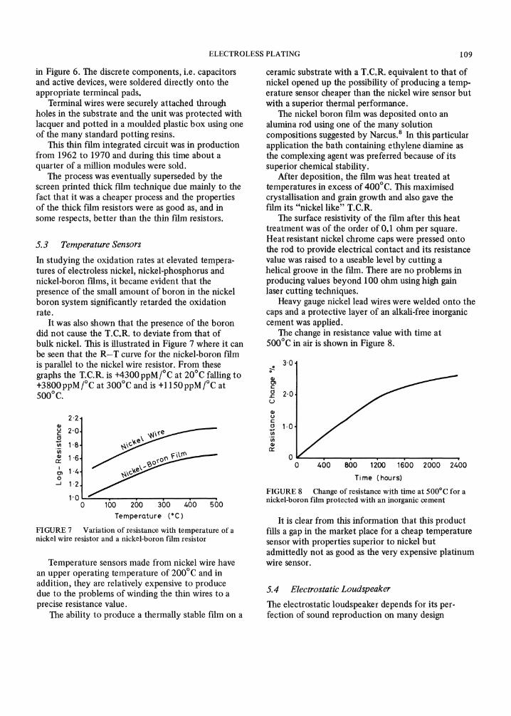
The change in resistance value with time at500C in air is shown in Figure 8.
3.0
2.0
o oo oo zoo 6oo o’oo b0Ti me (hours)
FIGURE 8 Change of resistance with time at 500C for anickel-boron film protected with an inorganic cement
It is clear from this information that this productfills a gap in the market place for a cheap temperaturesensor with properties superior to nickel butadmittedly not as good as the very expensive platinumwire sensor.
5.4 Electrostatic Loudspeaker
The electrostatic loudspeaker depends for its per-fection of sound reproduction on many design
110 J. DEARDEN
features but one of these looms high on the list ofrequirements and that is the efficiency of couplingbetween the vibrating Mylar diaphragm and thesurrounding air. This in turn demands a uniformelectrostatic field across the electrode gap.
One way of achieving this uniformity was to applya high surface resistivity layer uniformly over theentire surface of the diaphragm so that all incidentalleakage paths were over-ridden by this lowerresistivity "spreader".
An adequate level of surface resistivity was statedto be within 10a and 1010 ohm per square but inproducing this film it was made clear that the addedweight to the diaphragm must be minimal because ofits possible damping effect on the diaphragmvibration. At this time problems were beingexperienced using a conductor loaded resin layerwhere the value was achievable but the weight wastoo high.
The obvious answer was to apply a very thin,almost weightless layer, of a metal conductor. Thediaphragms were, however, far too big (2 ft. long x7 in wide) to be accommodated in a vacuum bell jarsuch that a uniform film could be evaporated orsputtered over the entire surface
Electrolessly deposited films did look as thoughthey could be the answer to the uniformity require-ment because the diaphragm could be formed intothe base of the metallising vessel by sticking a plasticwall around the edge of the diaphragm frame andplating over the whole surface of the diaphragm.
Conventional activation, followed by shortexposures to nickel-phosphorus plating solutionsproduced the required average resistivity but did notgive a sufficient degree of uniformity and so thisapproach had to be abandoned.
However, during the course of this work it wasnoted that under certain conditions of activation thecolourless Mylar diaphragms assumed a veryuniform brown colouration which, when dried out,had a resistivity in the required range of 108 to010 ohm per square and which showed little or no
variation over the entire surface of the diaphragm.A study was made of the factors which favoured
the deposition of the film and the variants whichdictated the ultimate value of the resistivity.
Using separate treatments firstly of stannouschloride solution and then palladium chloride solutiongave no measureable film deposition. However, theuse of an acidic colloidal suspension of palladiumprepared by using an admixture of palladium andstannous chlorides in a strong solution of hydro-chloric acid produced the desired film with the
lOlo
._>
1E5-C-
u’) 1090 400 800 1200 1600 2000 2400 2800
Time (hours)
FIGURE 9 Change in resistance with time for a palladium-tin film on Mylar at room temperature and 155C.
preferred resistivity. The film was shown to be amixture of elemental palladium and stannic acid.
It was shown that the surface resistivity achievedwas independent of the contact time providing it wasbeyond one minute and was also independent oftemperature within the range 25C to 80C. It was,however, dependent on the ratio of stannous chlorideto palladium chloride and by controlling this a pre-determined surface resistivity could be obtained.
The film was about 10 nm thick and thereforecame well within the maximum weight requirement.It was also shown that even in its unprotected statethe surface resistivity stayed well within its decadevalue when stored at room temperature for up to3000 hours. Even when exposed to a 155C ambientthe electrical stability was virtually unaltered (seeFigure 9).
6 CONCLUSIONS
From the work reported in this paper it can be seenthat there is no doubt about the usefulness of electro-lessly deposited "metal" films in the field of electro-nics. Only electroless plating appropriate to resistortechnology has been dealt with but it is clear that theproperties and processes can be manipulated over awide spectrum to satisfy a multitude of requirementsand will without doubt continue to provide solutionsto many other problems where thin film technologyis dominant.
REFERENCES
1. Wein, Metal Fnishing, November & December 1964.2. Wein, Metal Fnishing, January 1945.3. Wurtz, Comptes Rendres de l’Academie des Sciences
Vol. 18, April 1844, po 702; Vol. 21, p. 149, 1865.
ELECTROLESS PLATING 111
4. A. Brenner and G. E. Riddell, Journal of Research, Nat.Bureau ofStandards Vol. 39, Nov. 1947, p. 385- 395.
5. A. Brenner, Metal Finishing, December 1954, p. 61.6. G. Gutzeit, A.S. T.M. Special Technical Publication,
No. 265. Nov. 1959, p. 3-12.7. J.W. Dini and P. R. Coronado, Plating, April 1967,
p. 385- 390.8. H. Narcus, Plating, April 1967, p. 380-381.9. British Patent 885,239.
10. J. Dearden, Electronic Components 1968, Feb.p. 178-182.
11. British Patent 1, 119, 741.12. P. L. Kirby, Electronic Components 1965, June
p. 521-526.13. British Patent, 1,347,549.14. W. Goldie, Metallic Coating ofPlastics, Volume I: