80
ISO 9001 Registered ® Electroluminescent Lamp Drivers

ISO 9001 Registered
®
ElectroluminescentLamp Drivers
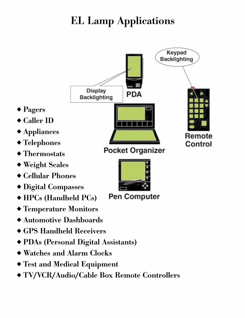
EL Lamp Applications
Pagers Caller ID Appliances Telephones Thermostats Weight Scales Cellular Phones Digital Compasses HPCs (Handheld PCs) Temperature Monitors Automotive Dashboards GPS Handheld Receivers PDAs (Personal Digital Assistants) Watches and Alarm Clocks Test and Medical Equipment TV/VCR/Audio/Cable Box Remote Controllers

Company Overview
© 2000 IMP, Inc. Electroluminescent Lamp Driver i
IMP, Inc. - Company ProfileIMP, Inc. designs, manufacturers and markets standard-setting analogintegrated circuits and specialty analog wafer foundry processes for datacommunications interface and power management applications in computer,communications and control systems. IMP products are sold through aworldwide network of representatives and distributors.
Company FacilitiesIMP headquarters and ISO 9001 certified wafer fabrication and test facility arelocated in San Jose, California. A product development center is located inPleasanton, California. The company employs 188 people.
Principal MarketsData Communications Interface – Data communications components, such asPCM digital switch and Small Computer Systems Interface (SCSI) terminatorintegrated circuits.
Power Management – Devices to generate, distribute, protect and managethermal and power consumption characteristics of desktop and portable com-puters, mobile and wireless communication devices, and battery poweredelectronic systems. Example products include electroluminescent lamp dri-vers, Universal Serial Bus (USB) power switches, microprocessor supervisors,low dropout voltage regulators, and high-frequency switching converters.
Wafer Fabrication and Manufacturing ServicesHigh-volume, analog and mixed-signal wafer foundry services on low-power,high-voltage, CMOS, BiCMOS, Bipolar and EEPROM processes, includingturnkey packaging and test capabilities. Fabrication services include databaseproduction using IMP standard processes, process development and portingof customer-owned technology.
For More InformationVisit the IMP web site at www.impweb.com; email [email protected] or contact IMP headquarters at 408.432.9100.

ii 408-432-9100/www.impweb.com © 2000 IMP, Inc. !

Table of Contents
© 2000 IMP, Inc. Electroluminescent Lamp Driver iii
Table of Contents
EL Driver Product Line Summary . . . . . . . . . . . . . . . . . . . . . . . . . . . . . . . . . . . iv
EL Lamp Driver Development Kits . . . . . . . . . . . . . . . . . . . . . . . . . . . . . . . .viii
Data Sheets
IMP522 . . . . . . . . . . . . . . . . . . . . . . . . . . . . . . . . . . . . . . . . . . . . . . . . . . . . . . . . 1
IMP525 . . . . . . . . . . . . . . . . . . . . . . . . . . . . . . . . . . . . . . . . . . . . . . . . . . . . . . . . 7
IMP527 . . . . . . . . . . . . . . . . . . . . . . . . . . . . . . . . . . . . . . . . . . . . . . . . . . . . . . . 13
IMP528 . . . . . . . . . . . . . . . . . . . . . . . . . . . . . . . . . . . . . . . . . . . . . . . . . . . . . . . 19
IMP560 . . . . . . . . . . . . . . . . . . . . . . . . . . . . . . . . . . . . . . . . . . . . . . . . . . . . . . . 25
IMP803 . . . . . . . . . . . . . . . . . . . . . . . . . . . . . . . . . . . . . . . . . . . . . . . . . . . . . . . 31
Die Specifications
IMP525 - Die Specifications . . . . . . . . . . . . . . . . . . . . . . . . . . . . . . . . . . . . . . 39
IMP527 - Die Specifications . . . . . . . . . . . . . . . . . . . . . . . . . . . . . . . . . . . . . . 40
IMP528 - Die Specifications . . . . . . . . . . . . . . . . . . . . . . . . . . . . . . . . . . . . . . 41
IMP560 - Die Specifications . . . . . . . . . . . . . . . . . . . . . . . . . . . . . . . . . . . . . . 42
IMP803 - Die Specifications . . . . . . . . . . . . . . . . . . . . . . . . . . . . . . . . . . . . . . 43
Application Notes
AN1 - IMP803 Evaluation Board . . . . . . . . . . . . . . . . . . . . . . . . . . . . . . . . . . 45
AN4 - EL Driver Demonstration Boards . . . . . . . . . . . . . . . . . . . . . . . . . . . . 51
Package Information . . . . . . . . . . . . . . . . . . . . . . . . . . . . . . . . . . . . . . . . . . . . . . 53
Tape and Reel Specifications . . . . . . . . . . . . . . . . . . . . . . . . . . . . . . . . . . . . . . . 54
IMP Sales Offices and Representatives . . . . . . . . . . . . . . . . . . . . . . . . . . . . . . 57
U.S. Distributors . . . . . . . . . . . . . . . . . . . . . . . . . . . . . . . . . . . . . . . . . . . . . . . . . 59
IMP International Sales Locations . . . . . . . . . . . . . . . . . . . . . . . . . . . . . . . . . . 60
Map to IMP - San Jose, CA, USA . . . . . . . . . . . . . . . . . . . . . . . . . . . . . . . . . . . 62
Quality at IMP - Our Policy . . . . . . . . . . . . . . . . . . . . . . . . . . . . . . . . . . . . . . . . 63
Power Management Products . . . . . . . . . . . . . . . . . . . . . . . . . . . . . . . . . . . . . . 65
µP Supervisor Products . . . . . . . . . . . . . . . . . . . . . . . . . . . . . . . . . . . . . . . 65-67
USB Power Switches . . . . . . . . . . . . . . . . . . . . . . . . . . . . . . . . . . . . . . . . . . . . 67
Sample Request Form . . . . . . . . . . . . . . . . . . . . . . . . . . . . . . . . . . . . . . . . . . . . . 68

EL Drive Product Line Summary
iv 408-432-9100/www.impweb.com © 2000 IMP, Inc. !
IMP Electroluminescent Lamp DriversIMP electroluminescent lamp drivers incorporate four EL lamp driving functions on-chip. These are the boost switch-mode power supply, its high-frequency oscillator, the high-voltage H-bridge lamp driver and its low-frequency oscillator. Few external componentsare needed: one inductor, one diode, one capacitor and two resistors. The resistors allow independent adjustment of boost converterfrequency and EL lamp drive frequency. Adjustable lamp drive frequency allows control over lamp color and power dissipation. Alldevices can be disabled for power saving.
All devices are available in chip form and small MicroSO and SO packages. Tape and reel shipment is available without additional cost.
–
+
525, 560, 803_01.eps
VDD1
LX4
CS3
VA7
VB6
RSW-OSC2 Switch
Oscillator
RegulationControl
IMP525IMP560IMP803
BridgeOutputDriver
Q
Q
Q
VREF
Lamp DriveOscillator
C
GND5
REL-OSC8
Q
522_01a.eps
–
+
LampDrive
Oscillator
Three-Level Detector
SelectA Lamp
SelectB Lamp
SwitchOscillator
VREF
(2) RSW-OSC
LX (4)
CS (3)
VA (8)
VAB (7)
VB (5)
DualBridgeDriverVDD
RegulationControl
(1) VDD
(9) LMPSEL
(10) REL-OSC
(6) GND
IMP522
EL Driver Product Line Summary
© 2000 IMP, Inc. Electroluminescent Lamp Driver v
The IMP525 Electroluminescent (EL) lamp driver is designed forsystems that must operate down to 1V and below. The input sup-ply voltage range is 0.9V to 2.5V. Typical output lamp drive volt-age is 112V peak-to-peak. EL lamps of up to 6nF capacitance canbe driven to high brightness.
A disable mode puts the chip into a low current-drain state. Whendisabled, quiescent current drops to 1µA typical with a VDD of1.5V. Connecting RSW, the oscillator frequency setting resistor, toground, can disable the chip. A disable pad, accessible only on thedie, can also be used to disable the driver (active low). An internalcircuit shuts down the switching regulator when the lamp drivevoltage exceeds 112V peak-to-peak. This conserves power andextends battery life.
Key Features Wide operating voltage range - from 0.9V to 2.5V Simple design requires few passive components 112V peak-to-peak typical AC output voltage Adjustable output frequency controls lamp color and
power consumption Adjustable converter frequency minimizes circuit
power consumption Disable mode extends battery life Disable current 1µA typical Compact MicroSO package and die option Same pinout as IMP803
IMP525: Single Cell Battery Powered Electroluminescent Lamp Driver/Inverter
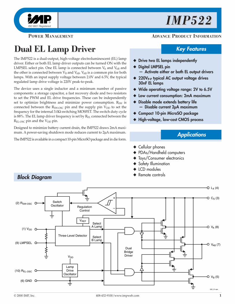
The IMP522 is a dual-output, high-voltage electroluminescent(EL) lamp driver. Either or both EL lamp driver outputs can beturned ON with the LMPSEL select pin. One EL lamp is connect-ed between VA and VAB and the other is connected between VB andVAB. VAB is a common pin for both lamps. With an input supplyvoltage between 2.0V and 6.5V, the typical regulated lamp drivevoltage is 220V peak-to-peak.
The device uses a single inductor and a minimum number of pas-sive components: a storage capacitor, a fast recovery diode andtwo resistors to set the PWM and EL drive frequencies. These canbeindependently set to optimize brightness and minimize powerconsumption. RSW is connected between the RSW-OSC pin and thesupply pin VDD to set the frequency for the internal 3.0Ω switch-ing MOSFET. The switch duty cycle is 88%. The EL lamp driverfrequency is set by REL connected between the REL-OSC pin and theVDD pin.
Designed to minimize battery current drain, the IMP522 draws 2mAmaximum. A power-saving shutdown mode reduces current to 2µAmaximum.
The IMP522 is available in a compact 10-pin MicroSO package and indie form.
Key Features Drive two EL lamps independently Digital LMPSEL pin
— Activate either or both EL output drivers 220VP-P typical AC output voltage drives
30nF EL lamps Wide operating voltage range: 2V to 6.5V Low current consumption: 22mA maximum Disable mode extends battery life
— Disable current 2µA maximum Compact 10-pin MicroSO package High-voltage, low-cost CMOS process
IMP522: Dual-Output, High-Voltage Electroluminescent Lamp Driver
EL Driver Product Line Summary
vi 408-432-9100/www.impweb.com © 2000 IMP, Inc. !
The IMP527 is an Electroluminescent (EL) lamp driver designedfor systems that must operate down to 1 volt and below. Theinput supply voltage range is 0.9V to 2.5V. Typical output lampdrive voltage is 180V. All four EL lamp-driving functions are on-chip. These are the switch-mode power supply, its high-frequen-cy oscillator, the high-voltage H-bridge lamp driver and its low-frequency oscillator. EL lamps of up to 6nF capacitance can bedriven to high brightness.The circuit requires few external components; one inductor, onediode, one capacitor and two resistors. The resistors set the fre-quency for the two oscillators.
A disable mode puts the chip into a low current-drain state. Whendisabled, quiescent current drops to 1µA typical with a VDD of1.5V. The chip can be disabled by connecting RSW, the oscillatorfrequency setting resistor, to ground. A disable pad (active low),accessible only on the die, can also be used to disable the driver.
An internal circuit shuts down the switching regulator when thelamp drive voltage exceeds 180V peak-to-peak. This conservespower and extends battery life.
The IMP527 is available in MicroSO and SO-8 packages and in die form.
Key Features Wide operating voltage range - from 0.9V to 2.5V Simple design requires few passive components 180V peak-to-peak typical AC output voltage Adjustable output frequency controls lamp color
and power consumption Adjustable converter frequency minimizes
circuit power consumption Disable mode extends battery life Disable current 1µA typical Compact MicroSO package option
IMP527: Single Cell Battery Powered Electroluminescent Lamp Driver/Inverter
The IMP528 is an Electroluminescent (EL) lamp driver with thefour EL lamp driving functions on-chip. These are the switch-mode power supply, its high-frequency oscillator, the high-volt-age H-bridge lamp driver and its low-frequency oscillator. TheIMP528 drives EL lamps of up to 50nF capacitance to high bright-ness; EL lamps with capacitances greater than 50nF can be driven,but will be lower in light output. The typical regulated outputvoltage that is applied to the EL lamp is 220V peak-to-peak. Thecircuit requires few external components; a single inductor, singlediode, two capacitors and three resistors. Two of these resistors set the frequency for two internal oscillators.
Unlike other EL lamp drivers, the IMP528 does not require anexternal protection resistor in series with the EL lamp.
The IMP528 operates over a 2.0V to 6.5V supply voltage range. Aregulated, low-power source can supply the low quiescent cur-rent of the IMP528. The inductor may be driven from an indepen-dent, unregulated supply voltage in dual supply applications.
An internal circuit shuts down the switching regulator when thelamp drive voltage reaches 220V peak-to-peak. This conservespower and extends battery life.
The IMP528 is available in MicroSO and SO-8 packages and in dieor wafer form.
Key Features 220V peak-to-peak typical AC output voltage Low Power: 420µA typical VDD current Wide operating voltage range- from 2.0V to 6.5V Large output load capability - drives lamps
with more than 50nF capacitance Eliminates external protection resistor in series
with EL lamp Adjustable output lamp frequency for control of
lamp color, lamp life, and power consumption Adjustable converter frequency to minimize
power consumption High-Voltage CMOS Process MicroSO package option
IMP528: High-Voltage EL Lamp Driver

EL Driver Product Line Summary
© 2000 IMP, Inc. Electroluminescent Lamp Driver vii
The IMP560 is designed for systems with modest EL lamp drive voltage requirements. It is ideal for low ambient light applicationsor where small lamps are used. With just one-half the inductorcurrent of the IMP803, the IMP560 reduces system power consumption and extends battery life. Input supply voltage rangeis 2.0V to 6.5V and quiescent current is a low 420µA. Typical ELlamp drive voltage is 120V peak-to-peak.
An internal circuit shuts down the switching regulator when thelamp drive voltage exceeds 120V peak-to-peak. This conservespower and extends battery life.
A disable mode puts the chip into a low current drain mode. Witha 3.0V supply, quiescent current drops to 200nA maximum, 50nAtypical.
Key Features 120V peak-to-peak typical AC output voltage Low input current (w/inductor current)......12mA Low disabled input current......50nA Wide operating voltage range - from 2.0V to 6.5V Simple design requires few passive components Adjustable output lamp frequency controls lamp color
and power consumption Adjustable converter frequency for minimum power
consumption IMP803 pin compatible MicroSO package option
IMP560: Power Efficient EL Lamp Driver
The IMP803 drives EL lamps of up to 30nF capacitance to highbrightness. EL lamps with capacitance greater than 30nF can bedriven but will be less bright. The typical regulated output volt-age that is applied to the EL lamp is 180V peak-to-peak.
The IMP803 operates over a 2.0V to 6.5V supply voltage range. A regulated, low-power source can supply the low quiescent current of the IMP803. The inductor may be driven from an inde-pendent, unregulated supply voltage in dual supply applications.An internal circuit shuts down the switching regulator when thelamp drive voltage reaches 180V peak-to-peak. This conservespower and extends battery life.
Key Features Low Power: 420µA typical VDD current Wide operating voltage range - from 2.0V to 6.5V 180V peak-to-peak typical AC output voltage Large output load capability - drive lamps with more
than 30nF capacitance Adjustable output lamp frequency for control of lamp
color, lamp life, and power consumption Adjustable converter frequency to minimize power
consumption Device can be Enabled/Disabled Low quiescent current - 20nA (disabled) High-Voltage CMOS Process MicroSO package option
IMP803: High-Voltage EL Lamp Driver
EL Lamp Driver Product Summary Table
traPtupnI
egnaRegatloV)V(
lacipyTegatloVtuptuO
V( PP )
detalugeRegatloVtuptuO
pmaLelbatsujdAtsooBdnaevirD
ycneuqerF
rewoPwoLedoMelbasiD
segakcaP
225PMI 5.6ot0.2022
)stuptuOlauD(seY seY seY OSorciM,nip-01
525PMI 5.2ot9.0 211 seY seY seY OS&OSorciM,nip-8
725PMI 5.2ot9.0 081 seY seY seY OS&OSorciM,nip-8
825PMI 5.6ot0.2 022 seY seY seY OS&OSorciM,nip-8
065PMI 5.6ot0.2 021 seY seY seY OS&OSorciM,nip-8
308PMI 5.6ot0.2 081 seY seY seY OS&OSorciM,nip-8
.elbaliavaoslaeraeiD 60t_B/DLE
!t
EL Driver Product Line Summary
viii 408-432-9100/www.impweb.com © 2000 IMP, Inc. !
EL Lamp Driver Development Kits
Several demonstration boards and evaluation kits are available to reduce time-to-market. The kits are available by calling IMPCustomer Service at 408.432.9100.
metI egakcaP/eciveD noitpircseD
1VE308PMI GL308PMI .draobnoitaulavE
MBDxxxPMI OSorciMynA .tiucric-ni)s(elpmasCIgnitaulaveroF.draobtnempoleveD
SBDxxxPMI OSynA .tiucric-ni)s(elpmasCIgnitaulaveroF.draobtnempoleveD50t_B/DLE
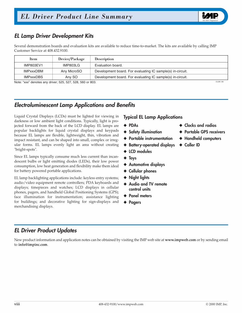
Electroluminescent Lamp Applications and Benefits
Liquid Crystal Displays (LCDs) must be lighted for viewing indarkness or low ambient light conditions. Typically, light is pro-jected forward from the back of the LCD display. EL lamps arepopular backlights for liquid crystal displays and keypadsbecause EL lamps are flexible, lightweight, thin, vibration andimpact resistant, and can be shaped into small, complex or irreg-ular forms. EL lamps evenly light an area without creating"bright-spots".
Since EL lamps typically consume much less current than incan-descent bulbs or light emitting diodes (LEDs), their low powerconsumption, low heat generation and flexibility make them idealfor battery powered portable applications.
EL lamp backlighting applications include: keyless entry systems;audio/video equipment remote controllers; PDA keyboards anddisplays; timepieces and watches; LCD displays in cellularphones, pagers, and handheld Global Positioning Systems (GPS);face illumination for instrumentation; assistance lighting for buildings; and decorative lighting for sign-displays and merchandising displays.
Typical EL Lamp Applications
PDAs Safety illumination Portable instrumentation Battery-operated displays LCD modules Toys Automotive displays Cellular phones Night lights Audio and TV remote
control units Panel meters Pagers
Clocks and radios Portable GPS receivers Handheld computers Caller ID
EL Driver Product UpdatesNew product information and application notes can be obtained by visiting the IMP web site at www.impweb.com or by sending emailto [email protected].
Note: “xxx” denotes any driver; 525, 527, 528, 560 or 803.
!t
© 2000 IMP, Inc. 408-432-9100/www.impweb.com 1
IMP522IMP522POWER MANAGEMENT ADVANCE PRODUCT INFORMATION
Dual EL LamDual EL Lamp Drp Driviverer
Cellular phones PDAs/Handheld computers Toys/Consumer electronics Safety Illumination LCD modules Remote controls
Drive two EL lamps independently Digital LMPSEL pin
— Activate either or both EL output drivers 220VP-P typical AC output voltage drives
30nF EL lamps Wide operating voltage range: 2V to 6.5V Low current consumption: 2mA maximum Disable mode extends battery life
— Disable current 2µA maximum Compact 10-pin MicroSO package High-voltage, low-cost CMOS process
Key Features
Applications
522_01.eps
–
+
LampDrive
Oscillator
Three-Level Detector
SelectA Lamp
SelectB Lamp
SwitchOscillator
VREF
(2) RSW-OSC
LX (4)
CS (3)
VA (8)
VAB (7)
VB (5)
DualBridgeDriverVDD
RegulationControl
(1) VDD
(9) LMPSEL
(10) REL-OSC
(6) GND
The IMP522 is a dual-output, high-voltage electroluminescent (EL) lampdriver. Either or both EL lamp driver outputs can be turned ON with theLMPSEL select pin. One EL lamp is connected between VA and VAB andthe other is connected between VB and VAB. VAB is a common pin for bothlamps. With an input supply voltage between 2.0V and 6.5V, the typicalregulated lamp drive voltage is 220V peak-to-peak.
The device uses a single inductor and a minimum number of passivecomponents: a storage capacitor, a fast recovery diode and two resistorsto set the PWM and EL drive frequencies. These can be independently set to optimize brightness and minimize power consumption. RSW is connected between the RSW-OSC pin and the supply pin VDD to set the frequency for the internal 3.0Ω switching MOSFET. The switch duty cycleis 88%. The EL lamp driver frequency is set by REL connected between theREL-OSC pin and the VDD pin.
Designed to minimize battery current drain, the IMP522 draws 2mA maxi-mum. A power-saving shutdown mode reduces current to 2µA maximum.
The IMP522 is available in a compact 10-pin MicroSO package and in die form.
Block Diagram

I M P 5 2 2I M P 5 2 2
2 408-432-9100/www.impweb.com © 2000 IMP, Inc.
Parameter Symbol Conditions Min Typ Max UnitsON-resistance of MOS Switch RDS(ON) I = 100mA 3.5 8 ΩOutput Voltage Regulation VCSREG 110 120 VOutput Voltage Peak-to-Peak (in regulation) VA-VAB, VB-VAB VDD = 2.0 to 6.5V 220 VOutput Drive Frequency (either output) fEL See Figure 1 2 µASwitching Frequency fSW See Figure 1 61 kHzSwitching Duty Cycle DSW See Figure 1 88 %
Input Current:IDD Without Inductor Current IIN0 See Figure 1 1.0 2.0 mAIDD Plus Inductor Current (1 Load) IIN1 See Figure 1 21 31
IDD Plus Inductor Current (2 Load) IIN2 See Figure 1 TBD TBD
4LX
3CS
2RSW-OSC
1VDD
7
LMPSEL
5VB 6 GND
8
VAB
9
VA
10 REL-OSC
522_02.eps
IMP522
MicroSO
Part Number Input Voltage Temperature Range Pins-Package IMP522EMB 2.0V to 6.5V –40°C to +85°C 10-MicroSO
VDD, RSW-OSC and REL-OSC . . . . . . . . . . . . . . . . . –0.5V to +7.0VCS, LX . . . . . . . . . . . . . . . . . . . . . . . . . . . . . . . . . –0.5V to +120VOperating Temperature Range . . . . . . . . . . . . –40°C to +85°CStorage Temperature Range . . . . . . . . . . . . . . –65°C to +150°CPower Dissipation (MicroSO) . . . . . . . . . . . . . 500mWVA, VB, VAB . . . . . . . . . . . . . . . . . . . . . . . . . . . . . –0.5V to VCS (pin 3)
Unless otherwise noted, VDD = 3.0V, RSW = 910kΩ, REL = 2.7MΩ, L = 220µH and TA = 25°C.
Note: All voltages are referenced to GND.
These are stress ratings only and functional operation is notimplied. Exposure to absolute maximum ratings for prolongedtime periods may affect device reliability.
Add /T to ordering part number for Tape and Reel.
Ordering Information
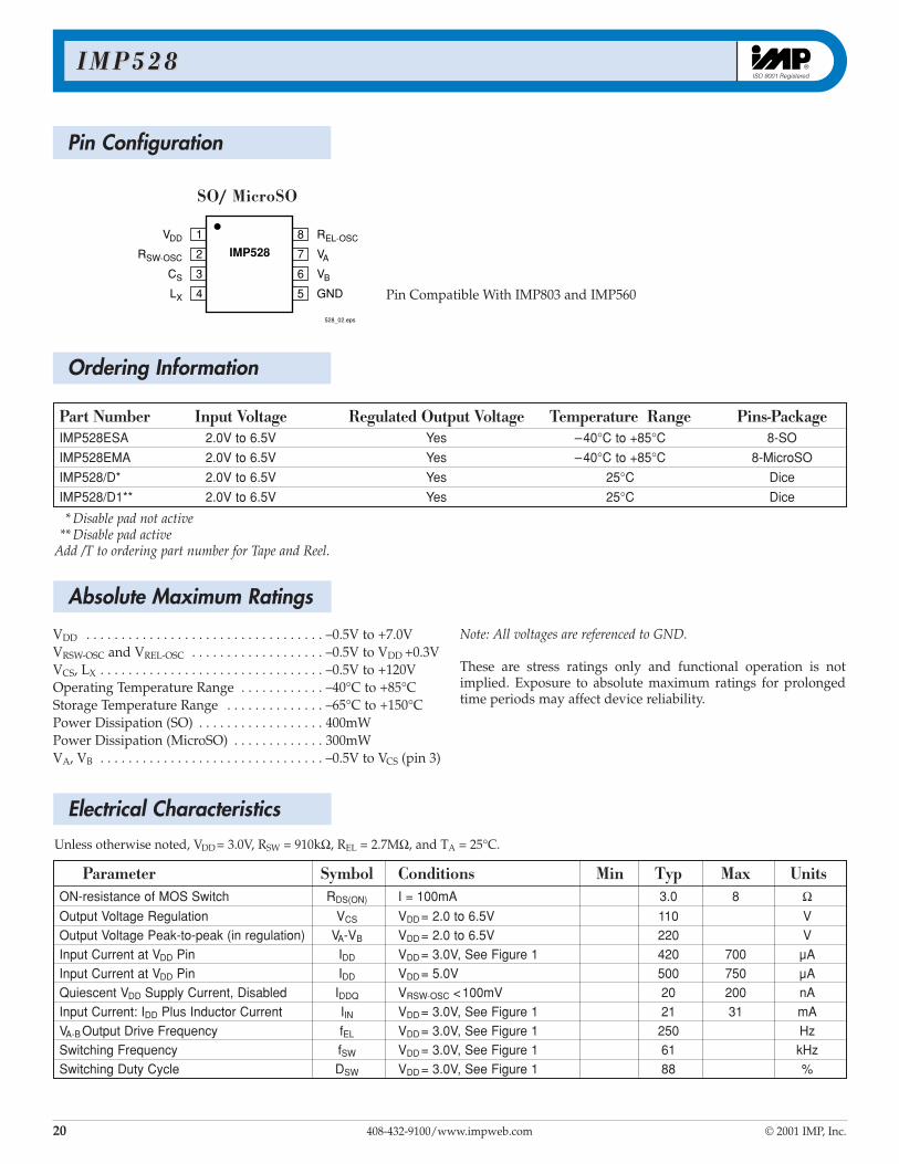
Pin Configuration
Absolute Maximum Ratings
Electrical Characteristics
I M P 5 2 2I M P 5 2 2
© 2000 IMP, Inc. Electroluminescent Lamp Drivers 3
Pin Descriptions
rebmuNniP emaN noitcnuF1 V DD detalugernuetarapesaotroerehdetcennocebyamLrotcudnI.ylppusegatlovevitisoP
.ylppus
2 R CSO-WS RrotsiserlanretxeehT.niprotsiseredom-hctiwS WS .ycneuqerfgnihctiwssenimreted
3 CS lauqeyletamixorppasipmalLEehtssorcaegatlovehT.roticapacegarotsretrevnoctsooBCtaegatlovehteciwtot S.
4 LX .LrotcudnikcabylfotnoitcennoC
5 VB .BpmaLLEroftuptuO
6 DNG .dnuorG
7 V BA .spmalLEhtobroflanimretnommoC
8 VA .ApmaLLEroftuptuO
9 LESPML .spmalhtobroBpmalroApmalrehtietceleS.niptupnietats-eerhtlatigiD
01 R CSO-LE RrotsiserlanretxE.nipgnittesycneuqerfrotallicsopmalLEehT LE Votdetcennoc DD stes.spmalhtobrofycneuqerfevirdpmaLLEeht
spe.10t_225
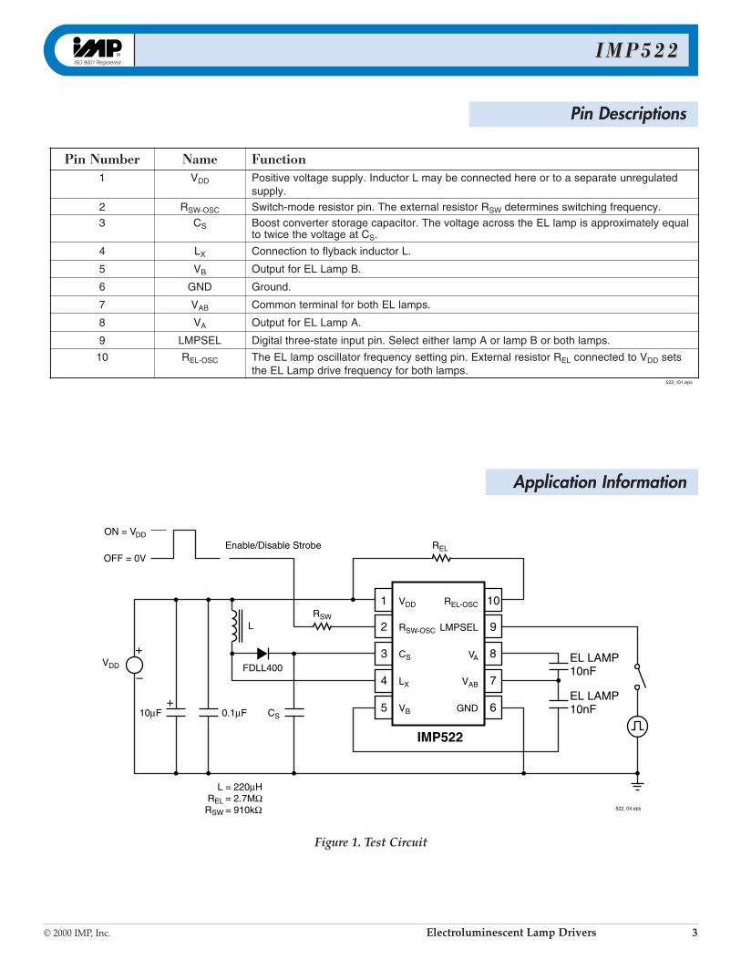
Figure 1. Test Circuit
Application Information
+
–
+
VDD
RSW-OSC
CS
LX
REL-OSC
VA
VAB
LMPSEL
VB GND
10
9
8
7
EL LAMP10nF
EL LAMP10nF
1
2
3
4
65
IMP522
RELEnable/Disable Strobe
VDD FDLL400
L
522_04.eps
ON = VDD
OFF = 0V
RSW
CS0.1µF10µF
L = 220µHREL = 2.7MΩ
RSW = 910kΩ
I M P 5 2 2I M P 5 2 2
4 408-432-9100/www.impweb.com © 2000 IMP, Inc.
Application Information
EL Lamp DriveThe outputs VA – VAB and VB – VAB are configured as H-bridges, driven by the EL oscillator. Each output is switched between CS
and ground on alternate phases, creating peak-to-peak signalsacross the EL lamps of twice the regulated voltage.
EL Lamp Selection: LMPSELThe digital input pin LMPSEL allows either or both EL lamps tobe active. Lamp A is active when LMPSEL is LOW and lamp B isactive when LMPSEL is HIGH. When LMPSEL is left floating ordriven by a three-state driver in the high impedance state, bothlamp driver outputs are active.
The logic HIGH signal level is defined as greater than 0.7VDD andlogic LOW is defined as less than 0.3VDD. A floating level is rec-ognized with the signal level between 0.3VDD and 0.7VDD, orwhen the output impedance of the driving voltage signal sourceis infinite (driver in OFF state).
Both drivers are OFF if the IMP522 is disabled.
LESPMLlangiS
evirDApmaLVA dna V BA
evirDBpmaLVB dna V BA
HGIH FFO NO
WOL NO FFO
/gnitaolFecnadepmIhgiH
NO NO
spe.20t_225
EL Driver Output Overvoltage RegulatorThe IMP522 maximum VCS output voltage is between 110V and120V. The internal overvoltage regulator skips the inductorswitching whenever the voltage on the CS pin exceeds the regula-tion threshold. The internal overvoltage detection trip point has ahysterisis of 1V and a range of 110V to 120V at room temperature.
PWM Circuit SwitchingThe switching MOSFET is driven by the PWM signal (nominally61kHz). During the first 88% of the period, the switch is ON, providing a low impedance path (<8Ω) from LX to ground. Thiscauses the external inductor to charge. In the last 12% of the period, the MOSFET is turned OFF. This causes the voltage on the output of LX to rise up to a high value. At some point, this willforward-bias the external diode, thus pumping charge into thestorage capacitor CS. The voltage on CS increases each cycle tobetween 110V and 120V. When the internal regulation trip-point isreached, the overvoltage regulator turns the MOSFET switch OFFto conserve power.

I M P 5 2 2I M P 5 2 2
© 2000 IMP, Inc. Electroluminescent Lamp Drivers 5
Power SequencingTo power up the chip, the RSW-OSC pin is connected to VDD throughthe external RSW resistor. The voltage on the pin will charge up toVDD/2. An internal threshold detector circuit monitors the pinvoltage and when it exceeds the threshold range (0.2V to 0.9V) itpowers up the oscillator and internal bias modules. This starts adelay counter which is one half of the EL oscillator period, afterwhich power to the high voltage internal modules is applied. TheIMP522 is then operating fully.
To power down the chip, RSW is driven to ground via a switch orlogic gate. When the voltage on the driver side of the resistor fallsbelow VDD/2, there will be no input bias current into the RSW-OSC
pin. This immediately powers down the internal high-voltage circuits, which effectively shuts the lamp off. At this point theoscillator and bias modules still draw quiescent current, but oscil-lations have ceased. As the RSW-OSC pin voltage falls below 0.1, theoscillator and bias modules are also fully powered down.
Figure 1. Driver Waveforms
522_03.eps
IN (Pulse)
ILX
VLX
Power Saving Disable ModeThe IMP522 can be powered up and down with RSW-OSC. In normal operation, this resistor on the RSW-OSC pin is connected toVDD or another voltage source. To power down (disable) theIMP522, RSW is connected to ground.
When disabled, the IMP522 quiescent current drops to typically 20nA.
In die form, an extra pin ENABLE is available (contact factory).Connecting this pad to VDD disables the chip. The ENABLE signalcan be driven by a microcontroller.
Oscillator Frequency AdjustmentThe EL lamp drive and PWM boost converter oscillation frequen-cies can be programmed independently.
The RSW resistor, connected between the RSW-OSC pin and VDD,determines the Inductor Switching (or PWM-) frequency. For therecommended nominal resistor value of 910kΩ, the frequency is61kHz. For other resistor values, the frequency is inversely pro-portional to the resistor value. Increasing the resistance will lowerthe frequency.
The REL resistor, connected between the REL-OSC pin and VDD,determines the EL lamp drive frequency. For the recommendednominal resistor value of 2.7MΩ, the frequency is 250Hz. Forother resistor values, the frequency is inversely proportional tothe resistor value: increasing the resistance will lower the fre-quency.
rotallicsO lanimoNrotsiseR
lanimoNycneuqerF
evirDpmaLLE R LE M7.2= Ω zH052
)MWP(hctiwSrotcudnI R WS k019= Ω zHk16spe.30t_225
Application Information

6 408-432-9100/www.impweb.com © 2000 IMP, Inc. !
Notes
Project
© 2000 IMP, Inc. 408-432-9100/www.impweb.com 7
IMP525IMP525POWER MANAGEMENT
SingSingle Cell Battle Cell Batterery Py PoowwererededElectrElectroluminescent Lamoluminescent LamppDrDriviver/Iner/Invverertterer
Audio/TV remote control units Pagers/Cellular phones PDAs Clocks and radios Portable GPS receivers LCD modules Toys
Wide operating voltage range - from 0.9V to 2.5V Simple design requires few passive components 112V peak-to-peak typical AC output voltage Adjustable output frequency controls lamp
color and power consumption Adjustable converter frequency minimizes
circuit power consumption Disable mode extends battery life Disable current 1µA typical Compact MicroSO package option
Block Diagram
–
+
525_01.eps
VDD1
LX4
CS3
VA7
VB6
RSW-OSC2 Switch
Oscillator
RegulationControl
IMP525 BridgeOutputDriver
Q
Q
Q
VREF
Lamp DriveOscillator
C
GND5
REL-OSC8
Q
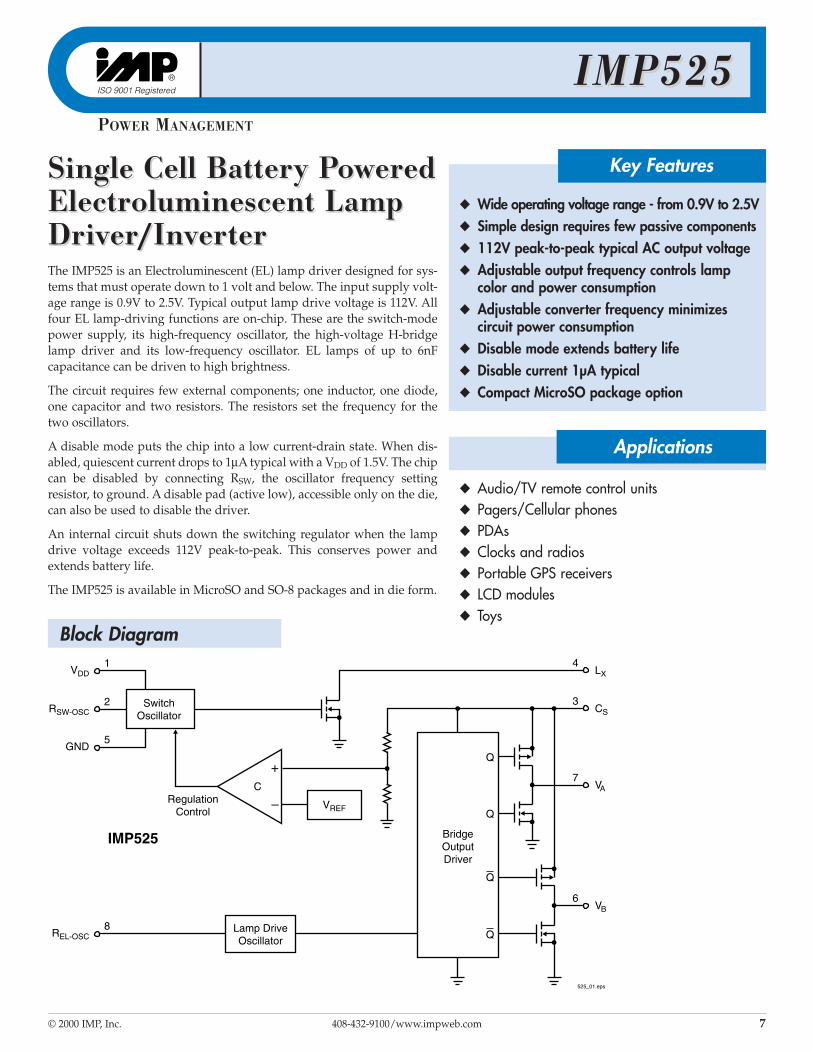
The IMP525 is an Electroluminescent (EL) lamp driver designed for sys-tems that must operate down to 1 volt and below. The input supply volt-age range is 0.9V to 2.5V. Typical output lamp drive voltage is 112V. Allfour EL lamp-driving functions are on-chip. These are the switch-modepower supply, its high-frequency oscillator, the high-voltage H-bridgelamp driver and its low-frequency oscillator. EL lamps of up to 6nFcapacitance can be driven to high brightness.
The circuit requires few external components; one inductor, one diode,one capacitor and two resistors. The resistors set the frequency for thetwo oscillators.
A disable mode puts the chip into a low current-drain state. When dis-abled, quiescent current drops to 1µA typical with a VDD of 1.5V. The chipcan be disabled by connecting RSW, the oscillator frequency setting resistor, to ground. A disable pad (active low), accessible only on the die,can also be used to disable the driver.
An internal circuit shuts down the switching regulator when the lampdrive voltage exceeds 112V peak-to-peak. This conserves power andextends battery life.
The IMP525 is available in MicroSO and SO-8 packages and in die form.
Key Features
Applications

I M P 5 2 5I M P 5 2 5
8 408-432-9100/www.impweb.com © 2000 IMP, Inc.
Parameter Symbol Conditions Min Typ Max UnitsON-resistance of MOS Switch RDS(ON) I = 50mA 15 ΩOperating Voltage 0.9 2.5 VOutput Voltage at CS VCS VDD = 1.5V, See Figure 1, Table 1 52 58 65 VOutput Voltage at CS VCS VDD = 0.9V, See Figure 1, Table 2 50 VOutput Voltage Peak-to-Peak VA-VB VDD = 1.5V, See Figure 1 104 112 124 VP-P
Quiescent VDD Supply Current, Disabled IQDIS Disable = HIGH 70 nA(Disable pin available on die only)Quiescent VDD Supply Current, Disabled IQDIS RSW-OSC = GND 1.0 2.0 µA
VDD = 1.5VInput Current at VDD Pin IDD VDD = 0.9V to 1.5V 1.5 mAInput Current: IDD Plus Inductor Current IIN VDD = 1.5V 23 32 mAVA-B Output Drive Frequency fEL VDD = 1.5V, See Figure 1, Table 1 500 HzBoost Converter Switching Frequency fSW VDD = 1.5V, See Figure 1, Table 1 26 kHzSwitching Duty Cycle DSW VDD = 1.5V, See Figure 1 87.5 %Disable Input LOW Voltage VDISL GND 0.2 V(Disable pin available on die only)Disable Input HIGH Voltage VDISH VDD-0.5V VDD V(Disable pin available on die only)
Ordering Information
Pin Configuration
4LX
3CS
2RSW-OSC
1VDD
5 GND
6 VB
7 VA
8 REL-OSC
525_02.eps
IMP525
SO/MicroSO
Part Number Input Voltage Regulated Output Voltage Temperature Range Pins-Package IMP525EMA 0.9V to 2.5V YES –40°C to +85°C 8-MicroSO
IMP525ESA 0.9V to 2.5V YES –40°C to +85°C 8-SO
IMP525/D* 0.9V to 2.5V YES 25°C Dice
IMP525/D1** 0.9V to 2.5V YES 25°C Dice
Absolute Maximum RatingsSupply Voltage, VDD, VRSW-OSC and VREL-OSC . . – 0.5V to +3.5VStorage Temperature Range . . . . . . . . . . . . . . . . – 65°C to +150°CPower Dissipation (SO package) . . . . . . . . . . . . 400mWPower Dissipation (MicroSO package) . . . . . . . 300mW
Unless otherwise noted, VDD = 1.5V, RSW = 1MΩ, REL = 1.0MΩ, and TA = 25°C.
Note: All voltages are referenced to GND.
These are stress ratings only and functional operation is not implied.Exposure to absolute maximum ratings for prolonged time periods mayaffect device reliability.
Electrical Characteristics
* Disable pad not active** Disable pad active
Add /T to ordering part number for Tape and Reel.
I M P 5 2 5I M P 5 2 5
© 2000 IMP, Inc. Electroluminescent Lamp Driver 9
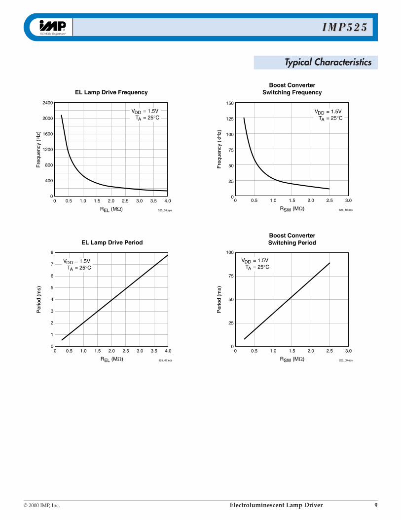
Typical Characteristics
Fre
quen
cy (
Hz)
REL (MΩ)
EL Lamp Drive Frequency
525_08.eps
VDD = 1.5VTA = 25°C
0 0.5 1.0 1.5 2.0 2.5 3.0 3.5 4.00
400
800
1200
1600
2000
2400
Fre
quen
cy (
kHz)
RSW (MΩ) 525_10.eps
0 0.5 1.0 1.5 2.0 2.5 3.00
25
50
75
100
125
150
Boost ConverterSwitching Frequency
VDD = 1.5VTA = 25°C
Per
iod
(ms)
REL (MΩ) 525_07.eps
0 0.5 1.0 1.5 2.0 2.5 3.0 3.5 4.00
1
2
3
4
5
6
7
8
EL Lamp Drive Period
VDD = 1.5VTA = 25°C
Per
iod
(ms)
RSW (MΩ) 525_09.eps
0 0.5 1.0 1.5 2.0 2.5 3.00
25
50
75
100
Boost ConverterSwitching Period
VDD = 1.5VTA = 25°C
I M P 5 2 5I M P 5 2 5
10 408-432-9100/www.impweb.com © 2000 IMP, Inc. !
Pin Descriptions
Pin Number Name Function1 VDD Positive voltage supply for the IMP525. Inductor L may be connected here or to a
separate supply.
2 RSW-OSC Switch-mode resistor pin. Switching frequency is determined by external resistor RSW, connected between pin 2 and VDD.
3 CS Boost converter storage capacitor. The voltage across the EL lamp is equal to twice the voltage at CS.
4 LX Connection to flyback inductance, L.
5 GND Ground pin.
6 VB EL lamp drive. The lamp is connected to a high-voltage bridge circuit with VB providing the complementary connection to VA.
7 VA EL lamp drive. (See above)
8 REL-OSC The EL lamp oscillator frequency-setting pin. The frequency is controlled by resistor REL, connected from pin 8 to VDD.
Disable Pad DIS Available only in die form. Setting DIS HIGH disables the chip.
External Component Description and Selection GuideDiode A fast reverse recovery diode, with BV > 100, such as a 1N4148.
Capacitor CS The high voltage capacitor that stores the inductive energy transferred through the catch diode. A 100 volt capacitor between 10nF and 100nF is recommended.
Resistor REL The EL lamp oscillator frequency-setting resistor. REL is connected between pin 8 and VDD, providing a frequency inversely proportional to REL; as REL increases, the EL lamp frequencydecreases along with the current drawn by the lamp. Lamp color is also determined by this frequency. A 1MΩ resistor between the REL-OSC pin and the VDD supply results in a lamp frequency around 500Hz.
Resistor RSW Switching Oscillator frequency-setting resistor. RSW is connected between the RSW-OSC pin and the VDD supply. The switching frequency is inversely proportional to the resistor value, dropping as the resistance increases.
Capacitor CSW This is an optional noise-suppression capacitor connected from ground to the RSW-OSC pin. A 100pF capacitor is recommended.
Inductor L The inductor provides the voltage boost needed by means of inductive “flyback”. The internalMOSFET switch alternately opens and closes the ground connection for the inductor at the LX pin. When the switch opens, the inductor potential will forward-bias the diode and the current will pass through to the storage capacitor CS, charging it to a high voltage.
As the value of the inductor is increased, the switching frequency set by RSW should also beincreased to prevent saturation. In general, smaller value inductors that can handle more currentare more desirable when larger-area EL lamps must be driven.
A small electrolytic capacitor (10µF, 16V), normally present across the inductor supply VIN, will likely eliminate the need for CSW.
External Components

I M P 5 2 5I M P 5 2 5
© 2000 IMP, Inc. Electroluminescent Lamp Driver 11
+
–
VDD
RSW-OSC
CS
LX
REL-OSC
VA
VB
GND
8
7
6
5
1
2
3
4
IMP525
REL
RSW
CS
VDD
0.1µF1
1N4148
D
L
3nF
Note:1. Larger values may be required depending upon supply impedance.
* Optional
525_03.eps
0.1µF100V
CSW*0.1nF
ON = VDD
OFF = 0V
Figure 1. Test Circuit
Test CircuitFigure 1 shows the IMP525 configured to drive an EL lamp, represented as a 3nF capacitor.
Application Information
Component Connections Value DescriptionRSW VDD, RSW-OSC 1MΩ Boost converter oscillator bias resistor
REL VDD, REL-OSC 1MΩ EL lamp driver oscillator bias resistor
L VDD, LX2 330µH2 Boost converter inductor
CS CS, GND 0.1µF/100V Boost converter storage capacitor
D LX, CS 1N4148 Switching diode
CSW RSW-OSC, GND 0.1nF Noise-suppression capacitor
Table 1. VIN = 1.5V
Notes. 2. Murata LQH4N331K04 (8.2Ω max. DCR)
Component Connections Value DescriptionRSW VDD, RSW-OSC 1.0MΩ Boost converter oscillator bias resistor
REL VDD, REL-OSC 2.62MΩ EL lamp driver oscillator bias resistor
L VDD, LX3 680µH3 Boost converter inductor
CS CS, GND 0.1µF/100V Boost converter storage capacitor
D LX, CS 1N4148 Switching diode
CSW RSW-OSC, GND 0.1nF Noise-suppression capacitor
Table 2. VIN = 0.9V
Notes. 3. Coilcraft DS1608C-684 (2.2Ω max. DCR)

I M P 5 2 5I M P 5 2 5
12 408-432-9100/www.impweb.com © 2000 IMP, Inc. !
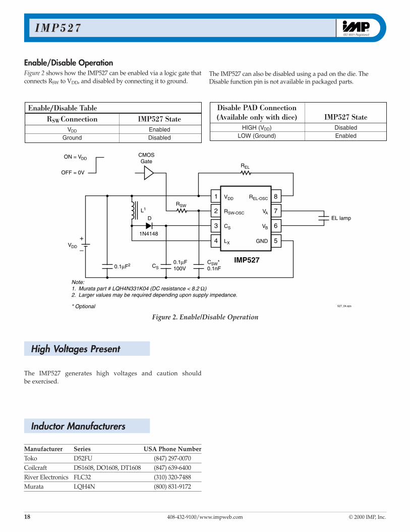
Enable/Disable OperationFigure 2 shows how the IMP525 can be enabled via a logic gate thatconnects RSW to VDD, and disabled by connecting it to ground.
RSW Connection IMP525 StateVDD Enabled
Ground Disabled
Figure 2. Enable/Disable Operation
Enable/Disable Table Disable PAD Connection(Available only with dice) IMP525 State
HIGH (VDD) DisabledLOW (Ground) Enabled
The IMP525 can also be disabled using a pad on the die. TheDisable function pin is not available in packaged parts.
+
–
VDD
RSW-OSC
CS
LX
REL-OSC
VA
VB
GND
8
7
6
5
1
2
3
4
IMP525
REL
CMOSGate
RSWL1
VDD
0.1µF2
1N4148
EL lamp
Note:1. Murata part # LQH4N331K04 (DC resistance < 8.2 Ω)2. Larger values may be required depending upon supply impedance.
* Optional 525_04.eps
ON = VDD
OFF = 0V
0.1µF100V
CSW*0.1nFCS
D
High Voltages Present
The IMP525 generates high voltages and caution should be exercised.
Manufacturer Series USA Phone NumberToko D52FU (847) 297-0070Coilcraft DS1608, DO1608, DT1608 (847) 639-6400River Electronics FLC32 (310) 320-7488Murata LQH4N (800) 831-9172
Inductor Manufacturers

© 2000 IMP, Inc. 408-432-9100/www.impweb.com 13
IMP52IMP5277POWER MANAGEMENT
SingSingle Cell Battle Cell Batterery Py PoowwererededElectrElectroluminescent Lamoluminescent LamppDrDriviver/Iner/Invverertterer
Audio/TV remote control units Pagers/Cellular phones PDAs Clocks and radios Portable GPS receivers LCD modules Toys
Wide operating voltage range - from 0.9V to 2.5V Simple design requires few passive components 180V peak-to-peak typical AC output voltage Adjustable output frequency controls lamp
color and power consumption Adjustable converter frequency minimizes
circuit power consumption Disable mode extends battery life Disable current 1µA typical Compact MicroSO package option
Key Features
Applications
Block Diagram
–
+
527_01.eps
VDD1
LX4
CS3
VA7
VB6
RSW-OSC2 Switch
Oscillator
RegulationControl
IMP527 BridgeOutputDriver
Q
Q
Q
VREF
Lamp DriveOscillator
C
GND5
REL-OSC8
Q
The IMP527 is an Electroluminescent (EL) lamp driver designed for systems that must operate down to 1 volt and below. The input supplyvoltage range is 0.9V to 2.5V. Typical output lamp drive voltage is 180V.All four EL lamp-driving functions are on-chip. These are the switch-mode power supply, its high-frequency oscillator, the high-voltage H-bridge lamp driver and its low-frequency oscillator. EL lamps of up to6nF capacitance can be driven to high brightness.
The circuit requires few external components; one inductor, one diode,one capacitor and two resistors. The resistors set the frequency for thetwo oscillators.
A disable mode puts the chip into a low current-drain state. When dis-abled, quiescent current drops to 1µA typical with a VDD of 1.5V. The chipcan be disabled by connecting RSW, the oscillator frequency setting resis-tor, to ground. A disable pad (active low), accessible only on the die, canalso be used to disable the driver.
An internal circuit shuts down the switching regulator when the lampdrive voltage exceeds 180V peak-to-peak. This conserves power andextends battery life.
The IMP527 is available in MicroSO and SO-8 packages and in die form.
I M P 5 2I M P 5 2 77
14 408-432-9100/www.impweb.com © 2000 IMP, Inc.
Parameter Symbol Conditions Min Typ Max UnitsON-resistance of MOS Switch RDS(ON) I = 50mA 15 ΩOperating Voltage 0.9 2.5 VOutput Voltage at CS VCS VDD = 1.5V, See Figure 1, Table 1 80 90 VOutput Voltage at CS VCS VDD = 0.9V, See Figure 1, Table 2 50 VOutput Voltage Peak-to-Peak VA-VB VDD = 1.5V, See Figure 1 180 VP-P
Quiescent VDD Supply Current, Disabled IQDIS Disable = HIGH 70 nA(Disable pin available on die only)Quiescent VDD Supply Current, Disabled IQDIS RSW-OSC = GND 1.0 2.0 µA
VDD = 1.5VInput Current at VDD Pin IDD VDD = 0.9V to 1.5V 1.5 mAInput Current: IDD Plus Inductor Current IIN VDD = 1.5V, See Figure 1, Table 1 26 32 mAVA-B Output Drive Frequency fEL VDD = 1.5V, See Figure 1, Table 1 500 HzBoost Converter Switching Frequency fSW VDD = 1.5V, See Figure 1, Table 1 26 kHzSwitching Duty Cycle DSW VDD = 1.5V, See Figure 1 87.5 %Disable Input LOW Voltage VDISL GND 0.2 V(Disable pin available on die only)Disable Input HIGH Voltage VDISH VDD-0.5V VDD V(Disable pin available on die only)
Ordering Information
Pin Configuration
4LX
3CS
2RSW-OSC
1VDD
5 GND
6 VB
7 VA
8 REL-OSC
527_02.eps
IMP527
SO/MicroSO
Part Number Input Voltage Regulated Output Voltage Temperature Range Pins-Package IMP527EMA 0.9V to 2.5V YES –40°C to +85°C 8-MicroSO
IMP527ESA 0.9V to 2.5V YES –40°C to +85°C 8-SO
IMP527/D* 0.9V to 2.5V YES 25°C Dice
IMP527/D1** 0.9V to 2.5V YES 25°C Dice
Absolute Maximum Ratings
Supply Voltage, VDD, VRSW-OSC and VREL-OSC . . – 0.5V to +3.5VStorage Temperature Range . . . . . . . . . . . . . . . . – 65°C to +150°CPower Dissipation (SO package) . . . . . . . . . . . . 400mWPower Dissipation (MicroSO package) . . . . . . . 300mW
Unless otherwise noted, VDD = 1.5V, RSW = 1MΩ, REL = 1MΩ, and TA = 25°C.
Note: All voltages are referenced to GND.
These are stress ratings only and functional operation is not implied.Exposure to absolute maximum ratings for prolonged time periods mayaffect device reliability.
Electrical Characteristics
* Disable pad not active** Disable pad active

I M P 5 2I M P 5 2 77
© 2000 IMP, Inc. Electroluminescent Lamp Driver 15
Typical Characteristics
Fre
quen
cy (
Hz)
REL (MΩ)
EL Lamp Drive Frequency
527_08.eps
VDD = 1.5VTA = 25°C
0 0.5 1.0 1.5 2.0 2.5 3.0 3.5 4.00
400
800
1200
1600
2000
2400
Fre
quen
cy (
kHz)
RSW (MΩ) 527_10.eps
0 0.5 1.0 1.5 2.0 2.5 3.00
25
50
75
100
125
150
Boost ConverterSwitching Frequency
VDD = 1.5VTA = 25°C
Per
iod
(ms)
REL (MΩ) 527_07.eps
0 0.5 1.0 1.5 2.0 2.5 3.0 3.5 4.00
1
2
3
4
5
6
7
8
EL Lamp Drive Period
VDD = 1.5VTA = 25°C
Per
iod
(ms)
RSW (MΩ) 527_09.eps
0 0.5 1.0 1.5 2.0 2.5 3.00
25
50
75
100
Boost ConverterSwitching Period
VDD = 1.5VTA = 25°C

I M P 5 2I M P 5 2 77
16 408-432-9100/www.impweb.com © 2000 IMP, Inc. !
Pin Descriptions
Pin Number Name Function1 VDD Positive voltage supply for the IMP527. Inductor L may be connected here or to a
separate supply.
2 RSW-OSC Switch-mode resistor pin. Switching frequency is determined by external resistor RSW, connected between pin 2 and VDD.
3 CS Boost converter storage capacitor. The voltage across the EL lamp is equal to twice the voltage at CS.
4 LX Connection to flyback inductance, L.
5 GND Ground pin.
6 VB EL lamp drive. The lamp is connected to a high-voltage bridge circuit with VB providing the complementary connection to VA.
7 VA EL lamp drive. (See above)
8 REL-OSC The EL lamp oscillator frequency-setting pin. The frequency is controlled by resistor REL, connected from pin 8 to VDD.
Disable Pad DIS Available only in die form. Setting DIS HIGH disables the chip.
External Component Description and Selection GuideDiode A fast reverse recovery diode, with BV > 100, such as a 1N4148.
Capacitor CS The high voltage capacitor that stores the inductive energy transferred through the catch diode. A 100 volt capacitor between 10nF and 100nF is recommended.
Resistor REL The EL lamp oscillator frequency-setting resistor. REL is connected between pin 8 and VDD, providing a frequency inversely proportional to REL; as REL increases, the EL lamp frequencydecreases along with the current drawn by the lamp. Lamp color is also determined by this frequency. A 1MΩ resistor between the REL-OSC pin and the VDD supply results in a lamp frequency around 500Hz.
Resistor RSW Switching Oscillator frequency-setting resistor. RSW is connected between the RSW-OSC pin and the VDD supply. The switching frequency is inversely proportional to the resistor value, dropping as the resistance increases.
Capacitor CSW This is an optional noise-suppression capacitor connected from ground to the RSW-OSC pin. A 100pF capacitor is recommended.
Inductor L The inductor provides the voltage boost needed by means of inductive “flyback”. The internalMOSFET switch alternately opens and closes the ground connection for the inductor at the LX pin. When the switch opens, the inductor potential will forward-bias the diode and the current will pass through to the storage capacitor CS, charging it to a high voltage.
As the value of the inductor is increased, the switching frequency set by RSW should also beincreased to prevent saturation. In general, smaller value inductors that can handle more currentare more desirable when larger-area EL lamps must be driven.
A small electrolytic capacitor (10µF, 16V), normally present across the inductor supply VIN, will likely eliminate the need for CSW.
External Components

I M P 5 2I M P 5 2 77
© 2000 IMP, Inc. Electroluminescent Lamp Driver 17
+
–
VDD
RSW-OSC
CS
LX
REL-OSC
VA
VB
GND
8
7
6
5
1
2
3
4
IMP527
REL
RSW
CS
VDD
0.1µF1
1N4148
D
L
3nF
Note:1. Larger values may be required depending upon supply impedance.
* Optional
527_03.eps
0.1µF100V
CSW*0.1nF
ON = VDD
OFF = 0V
Figure 1. Test Circuit
Test CircuitFigure 1 shows the IMP527 configured to drive an EL lamp, represented as a 3nF capacitor.
Component Connections Value DescriptionRSW VDD, RSW-OSC 1MΩ Boost converter oscillator bias resistor
REL VDD, REL-OSC 1MΩ EL lamp driver oscillator bias resistor
L VDD, LX2 330µH2 Boost converter inductor
CS CS, GND 0.1µF/100V Boost converter storage capacitor
D LX, CS 1N4148 Switching diode
CSW RSW-OSC, GND 0.1nF Noise-suppression capacitor (optional)
Table 1. VIN = 1.5V
Notes. 2. Murata LQH4N331K04 (8.2Ω max. DCR)
Component Connections Value DescriptionRSW VDD, RSW-OSC 1MΩ Boost converter oscillator bias resistor
REL VDD, REL-OSC 2.62MΩ EL lamp driver oscillator bias resistor
L VDD, LX3 680µH3 Boost converter inductor
CS CS, GND 0.1µF/100V Boost converter storage capacitor
D LX, CS 1N4148 Switching diode
CSW RSW-OSC, GND 0.1nF Noise-suppression capacitor (optional)
Table 2. VIN = 0.9V
Notes. 3. Coilcraft DS1608C-684 (2.2Ω max. DCR)
Application Information
I M P 5 2I M P 5 2 77
18 408-432-9100/www.impweb.com © 2000 IMP, Inc. !
Enable/Disable OperationFigure 2 shows how the IMP527 can be enabled via a logic gate thatconnects RSW to VDD, and disabled by connecting it to ground.
RSW Connection IMP527 StateVDD Enabled
Ground Disabled
Figure 2. Enable/Disable Operation
Enable/Disable Table Disable PAD Connection(Available only with dice) IMP527 State
HIGH (VDD) DisabledLOW (Ground) Enabled
The IMP527 can also be disabled using a pad on the die. TheDisable function pin is not available in packaged parts.
+
–
VDD
RSW-OSC
CS
LX
REL-OSC
VA
VB
GND
8
7
6
5
1
2
3
4
IMP527
REL
CMOSGate
RSWL1
VDD
0.1µF2
1N4148
EL lamp
Note:1. Murata part # LQH4N331K04 (DC resistance < 8.2 Ω)2. Larger values may be required depending upon supply impedance.
* Optional 527_04.eps
ON = VDD
OFF = 0V
0.1µF100V
CSW*0.1nFCS
D
High Voltages Present
The IMP527 generates high voltages and caution should be exercised.
Manufacturer Series USA Phone NumberToko D52FU (847) 297-0070Coilcraft DS1608, DO1608, DT1608 (847) 639-6400River Electronics FLC32 (310) 320-7488Murata LQH4N (800) 831-9172
Inductor Manufacturers

© 2001 IMP, Inc. 408-432-9100/www.impweb.com 19
IMP528IMP528POWER MANAGEMENT
Block Diagram
High-High-VVoltoltagage EL Lame EL Lamp Drp Driviverer– 220 V– 220 VPPPP DrDrivivee
GPS units/Pagers/Cellular phones PDAs/Handheld computers Safety illumination Portable instrumentation Battery-operated displays LCD modules Toys
220V peak-to-peak typical AC output voltage Low Power: 420µA typical VDD current Wide operating voltage range- from 2.0V to 6.5V Large output load capability - drives lamps
with more than 50nF capacitance Eliminates external protection resistor in series
with EL lamp Adjustable output lamp frequency for control of
lamp color, lamp life, and power consumption Adjustable converter frequency to minimize
power consumption High-Voltage CMOS Process MicroSO package option
Key Features
Applications
–
+
528_01.eps
VDD1
LX4
CS3
VA7
VB6
RSW-OSC2 Switch
Oscillator
RegulationControl
IMP528 BridgeOutputDriver
Q
Q
Q
VREF
Lamp DriveOscillator
C
GND5
REL-OSC8
Q
The IMP528 is an Electroluminescent (EL) lamp driver with the four ELlamp driving functions on-chip. These are the switch-mode power sup-ply, its high-frequency oscillator, the high-voltage H-bridge lamp driverand its low-frequency oscillator. The IMP528 drives EL lamps of up to50nF capacitance to high brightness; EL lamps with capacitances greaterthan 50nF can be driven, but will be lower in light output. The typicalregulated output voltage that is applied to the EL lamp is 220V peak-to-peak. The circuit requires few external components; a single inductor,single diode, two capacitors and two resistors. Two of these resistors set the frequency for two internal oscillators.
Unlike other EL lamp drivers, the IMP528 does not require an externalprotection resistor in series with the EL lamp.
The IMP528 operates over a 2.0V to 6.5V supply voltage range. Aregulated, low-power source can supply the low quiescent current of theIMP528. The inductor may be driven from an independent, unregulatedsupply voltage in dual supply applications.
An internal circuit shuts down the switching regulator when the lampdrive voltage reaches 220V peak-to-peak. This conserves power andextends battery life.
The IMP528 is available in MicroSO and SO-8 packages and in die orwafer form.
I M P 5 2 8I M P 5 2 8
20 408-432-9100/www.impweb.com © 2001 IMP, Inc.
Electrical Characteristics
Absolute Maximum Ratings
Ordering Information
Pin Configuration
Parameter Symbol Conditions Min Typ Max UnitsON-resistance of MOS Switch RDS(ON) I = 100mA 3.0 8 ΩOutput Voltage Regulation VCS VDD = 2.0 to 6.5V 110 VOutput Voltage Peak-to-peak (in regulation) VA-VB VDD = 2.0 to 6.5V 220 VInput Current at VDD Pin IDD VDD = 3.0V, See Figure 1 420 700 µAInput Current at VDD Pin IDD VDD = 5.0V 500 750 µAQuiescent VDD Supply Current, Disabled IDDQ VRSW-OSC <100mV 20 200 nAInput Current: IDD Plus Inductor Current IIN VDD = 3.0V, See Figure 1 21 31 mAVA-B Output Drive Frequency fEL VDD = 3.0V, See Figure 1 250 HzSwitching Frequency fSW VDD = 3.0V, See Figure 1 61 kHzSwitching Duty Cycle DSW VDD = 3.0V, See Figure 1 88 %
4LX
3CS
2RSW-OSC
1VDD
5 GND
6 VB
7 VA
8 REL-OSC
528_02.eps
IMP528
SO/ MicroSO
Part Number Input Voltage Regulated Output Voltage Temperature Range Pins-Package IMP528ESA 2.0V to 6.5V Yes –40°C to +85°C 8-SO
IMP528EMA 2.0V to 6.5V Yes –40°C to +85°C 8-MicroSO
IMP528/D* 2.0V to 6.5V Yes 25°C Dice
IMP528/D1** 2.0V to 6.5V Yes 25°C Dice
VDD . . . . . . . . . . . . . . . . . . . . . . . . . . . . . . . . . . –0.5V to +7.0VVRSW-OSC and VREL-OSC . . . . . . . . . . . . . . . . . . . –0.5V to VDD +0.3VVCS, LX . . . . . . . . . . . . . . . . . . . . . . . . . . . . . . . . –0.5V to +120VOperating Temperature Range . . . . . . . . . . . . –40°C to +85°CStorage Temperature Range . . . . . . . . . . . . . . –65°C to +150°CPower Dissipation (SO) . . . . . . . . . . . . . . . . . . 400mWPower Dissipation (MicroSO) . . . . . . . . . . . . . 300mWVA, VB . . . . . . . . . . . . . . . . . . . . . . . . . . . . . . . . –0.5V to VCS (pin 3)
Unless otherwise noted, VDD = 3.0V, RSW = 910kΩ, REL = 2.7MΩ, and TA = 25°C.
Note: All voltages are referenced to GND.
These are stress ratings only and functional operation is notimplied. Exposure to absolute maximum ratings for prolongedtime periods may affect device reliability.
Pin Compatible With IMP803 and IMP560
* Disable pad not active** Disable pad active
Add /T to ordering part number for Tape and Reel.
I M P 5 2 8I M P 5 2 8
© 2001 IMP, Inc. Electroluminescent Lamp Driver 21
Pin Descriptions
External Components
Pin Number Name Function1 VDD Positive voltage supply for the IMP528. Inductor L may be connected here or to a
separate unregulated supply.
2 RSW-OSC Switch-mode resistor pin. Switching frequency is determined by an external resistor, RSW.
3 CS Boost converter storage capacitor. The voltage across the EL lamp is equal to twice the voltage at CS.
4 LX Connection to flyback inductance, L.
5 GND Ground pin.
6 VB EL lamp drive. The lamp is connected in a high-voltage bridge circuit with VB providing the complementary connection to VA. The peak-to-peak AC voltage across the EL lamp is thus two times VCS.
7 VA EL lamp drive. (See above)
8 REL-OSC The EL lamp oscillator frequency setting pin. The oscillator frequency is controlled by external resistor REL.
External Component Description and Selection GuideDiode Catch diode. A fast reverse recovery diode, with BV > 150V, such as an FDLL400 (150V).
Capacitor CS This is the high voltage capacitor that stores the inductive energy transferred through the catch diode. A capacitor with WV > 120V between 10nF and 100nF is recommended.
Resistor REL The EL lamp oscillator frequency setting resistor. This resistor, connected between the REL-OSC pin and VDD, provides an oscillator frequency inversely proportional to REL; as REL increases, the EL lamp frequency decreases along with the current drawn by the lamp. Lamp color is also determined by this frequency. A 2.7MΩ resistor between the REL-OSC pin and the VDD supply results in a lamp frequency around 250Hz.
Resistor RSW Switching Oscillator frequency setting resistor. The switching oscillator resistor is connected between the RSW-OSC pin and the VDD supply. The switching frequency is inversely proportionalto the resistor value, dropping as the resistance increases.
Inductor L The inductor provides the voltage boost needed by means of inductive “flyback”. The internalMOSFET switch alternately opens and closes the ground connection for the inductor at the LX pin. When this internal switch opens, the inductor potential will forward-bias the catch diode and the current will pass through the storage capacitor CS, charging it to a high voltage.
Smaller inductors are preferred to prevent saturation. As the value of the inductor increases (and the series DC resistance of the inductor decreases), the switching frequency set by RSW should be increased to prevent saturation. In general, smaller value inductors thatcan handle more current are more desirable when larger area EL lamps must be driven.

I M P 5 2 8I M P 5 2 8
22 408-432-9100/www.impweb.com © 2001 IMP, Inc.
+
–
VDD
RSW-OSC
CS
LX
REL-OSC
VA
VB
GND
8
7
6
5
1
2
3
4
IMP528
2.7MΩ
REL
910kΩ220µH1
VIN = 3.0V
0.1µF2
FDLL400
LL EN3
EL lamp10nF(3 in2 lamp)
Note:1. Murata part # LQH4N221K04 (DC resistance <5Ω)2. Larger values may be required depending upon supply impedance.3. EN is connected to VDD to enable and to GND to disable.
528_03.eps
10nF200V
RSW
CS
Figure 1. 3.0V Application
Test and Application Circuit, 3.0VFigure 1 shows the IMP528 configured to drive an EL lamp with a3.0V input.
Dual Supply Operation with 1.5V BatteryThe IMP528 can also be operate from a single battery cell when aregulated voltage higher than 2.0V is also available. This dualsupply configuration, shown in Figure 2, uses the regulated
voltage to operate the IMP528 while the energy for the high-voltage boost circuit comes from the battery.
+
–
EN2
VDD
RSW-OSC
CS
LX
REL-OSC
VA
VB
GND
8
7
6
5
1
2
3
4
IMP528
REL
Regulated Voltage(2.0V to 6.5V)
RSW
VIN
L
BatteryVoltage
0.1µF1
FDLL400
EL lamp
528_04.eps1. Larger values may be required depending upon supply impedance.2. EN is connected to VDD to enable and to GND to disable.
10nF200VCS
Figure 2. Dual Supply Operation
Application Information

I M P 5 2 8I M P 5 2 8
© 2001 IMP, Inc. Electroluminescent Lamp Driver 23
High–Voltages Present
Switch ResistanceThe IMP528 inductor switch resistance is typically below 3.5Ω, asshown in Figure 3.
On
Res
ista
nce
(Ω)
VDD (V) 528_05.eps
1 2 3 4 5 6 70
5
10
15
20
25
30
Figure 3. Boost Switch ON-Resistance
The IMP528 generates high voltages and caution should be exercised.

24 408-432-9100/www.impweb.com © 2001 IMP, Inc.
Notes
Project
© 2000 IMP, Inc. 408-432-9100/www.impweb.com 25
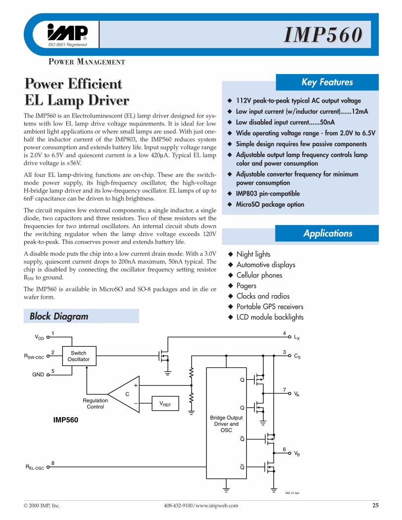
IMP560IMP560POWER MANAGEMENT
PPoowwer Efer Effficient icient EL LamEL Lamp Drp Driviverer
Night lights Automotive displays Cellular phones Pagers Clocks and radios Portable GPS receivers LCD module backlights
112V peak-to-peak typical AC output voltage
Low input current (w/inductor current)......12mA
Low disabled input current......50nA
Wide operating voltage range - from 2.0V to 6.5V
Simple design requires few passive components
Adjustable output lamp frequency controls lampcolor and power consumption
Adjustable converter frequency for minimumpower consumption
IMP803 pin-compatible
MicroSO package option
Block Diagram
–
+
560_01.eps
VDD1
LX4
CS3
VA7
VB6
RSW-OSC2 Switch
Oscillator
RegulationControl
IMP560 Bridge OutputDriver and
OSC
Q
Q
Q
VREF
C
GND5
REL-OSC8
Q
The IMP560 is an Electroluminescent (EL) lamp driver designed for sys-tems with low EL lamp drive voltage requirements. It is ideal for lowambient light applications or where small lamps are used. With just one-half the inductor current of the IMP803, the IMP560 reduces systempower consumption and extends battery life. Input supply voltage rangeis 2.0V to 6.5V and quiescent current is a low 420µA. Typical EL lampdrive voltage is ±56V.
All four EL lamp-driving functions are on-chip. These are the switch-mode power supply, its high-frequency oscillator, the high-voltage H-bridge lamp driver and its low-frequency oscillator. EL lamps of up to6nF capacitance can be driven to high brightness.
The circuit requires few external components; a single inductor, a singlediode, two capacitors and three resistors. Two of these resistors set thefrequencies for two internal oscillators. An internal circuit shuts downthe switching regulator when the lamp drive voltage exceeds 120V peak-to-peak. This conserves power and extends battery life.
A disable mode puts the chip into a low current drain mode. With a 3.0Vsupply, quiescent current drops to 200nA maximum, 50nA typical. Thechip is disabled by connecting the oscillator frequency setting resistorRSW to ground.
The IMP560 is available in MicroSO and SO-8 packages and in die orwafer form.
Key Features
Applications
I M P 5 6 0I M P 5 6 0
26 408-432-9100/www.impweb.com © 2000 IMP, Inc.
Parameter Symbol Conditions Min Typ Max UnitsON-resistance of MOS Switch RDS(ON) I = 100mA 3.5 8 ΩOutput Voltage Regulation VCS VDD = 2.0 to 6.5V 52 56 65 VOutput Voltage Peak-to-peak (in regulation) VA-VB VDD = 2.0 to 6.5V 104 112 120 VQuiescent VDD Supply Current, Disabled IDDIS VRSW-OSC <100mV 50 200 nAInput Current at VDD Pin IDD VDD = 3.0V, See Figure 1 470 700 µAInput Current at VDD Pin IDD VDD = 5.0V, See Figure 2 500 750 µAInput Current: IDD Plus Inductor Current IIN VDD = 3.0V, See Figure 1 12 mAVA-B Output Drive Frequency fEL VDD = 3.0V, See Figure 1 300 370 430 HzSwitching Frequency fSW VDD = 3.0V, See Figure 1 50 70 90 kHzSwitching Duty Cycle DSW VDD = 3.0V, See Figure 1 88 %
Ordering Information
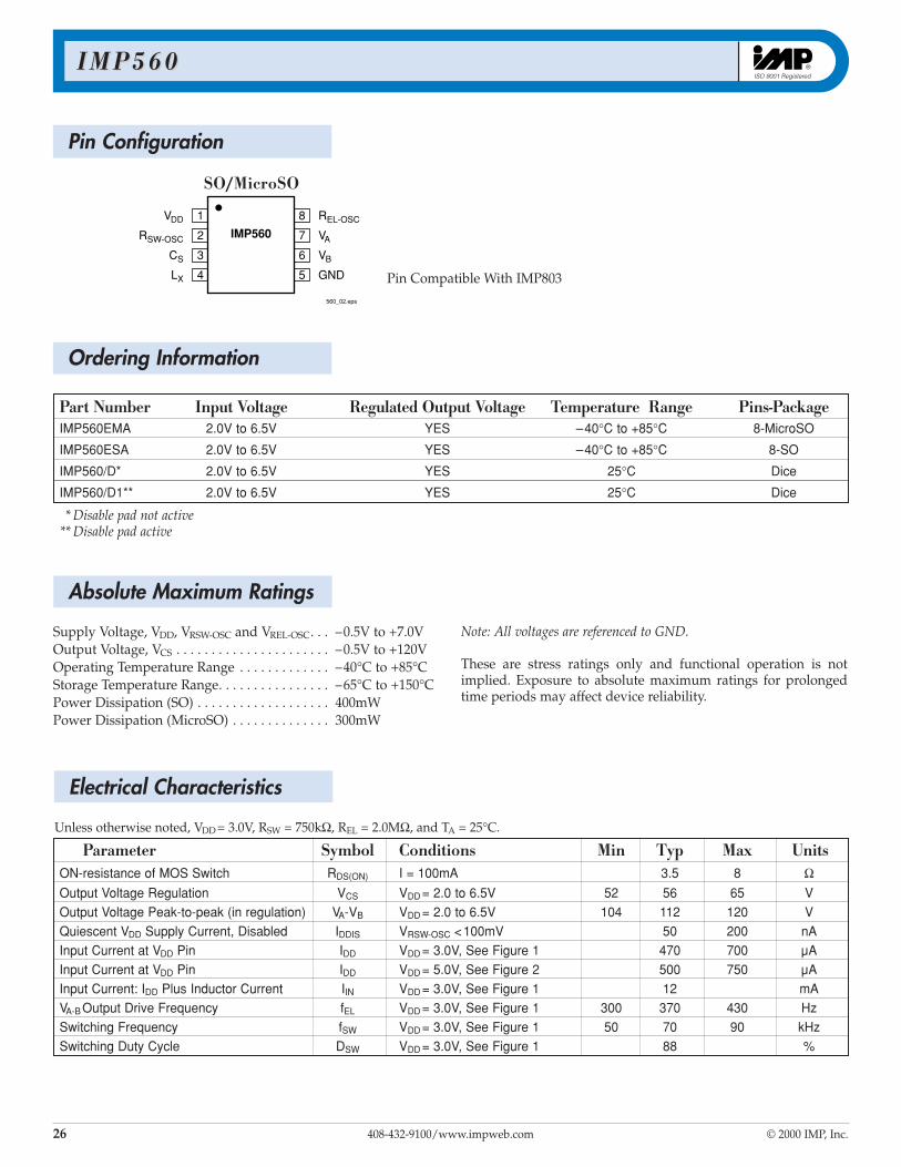
Pin Configuration
4LX
3CS
2RSW-OSC
1VDD
5 GND
6 VB
7 VA
8 REL-OSC
560_02.eps
IMP560
SO/MicroSO
Part Number Input Voltage Regulated Output Voltage Temperature Range Pins-Package IMP560EMA 2.0V to 6.5V YES –40°C to +85°C 8-MicroSO
IMP560ESA 2.0V to 6.5V YES –40°C to +85°C 8-SO
IMP560/D* 2.0V to 6.5V YES 25°C Dice
IMP560/D1** 2.0V to 6.5V YES 25°C Dice
Absolute Maximum Ratings
Supply Voltage, VDD, VRSW-OSC and VREL-OSC. . . –0.5V to +7.0VOutput Voltage, VCS . . . . . . . . . . . . . . . . . . . . . . –0.5V to +120VOperating Temperature Range . . . . . . . . . . . . . –40°C to +85°CStorage Temperature Range. . . . . . . . . . . . . . . . –65°C to +150°CPower Dissipation (SO) . . . . . . . . . . . . . . . . . . . 400mWPower Dissipation (MicroSO) . . . . . . . . . . . . . . 300mW
Electrical Characteristics
Unless otherwise noted, VDD = 3.0V, RSW = 750kΩ, REL = 2.0MΩ, and TA = 25°C.
Note: All voltages are referenced to GND.
These are stress ratings only and functional operation is notimplied. Exposure to absolute maximum ratings for prolongedtime periods may affect device reliability.
Pin Compatible With IMP803
* Disable pad not active** Disable pad active
I M P 5 6 0I M P 5 6 0
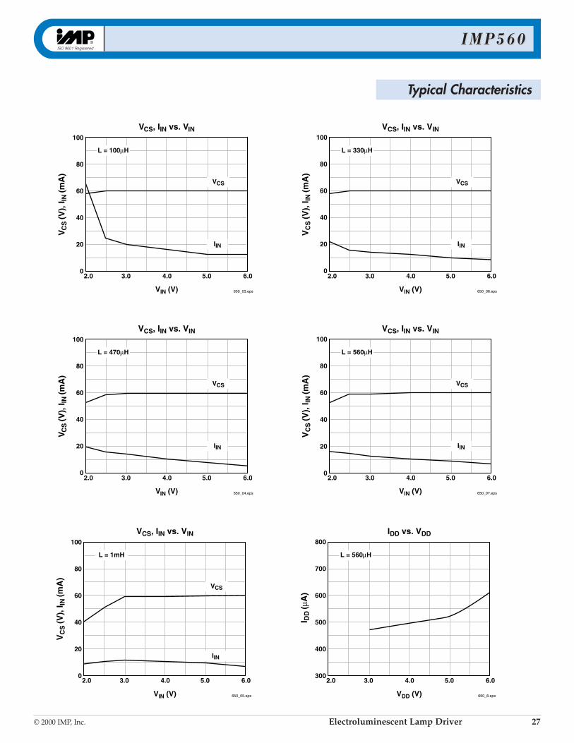
© 2000 IMP, Inc. Electroluminescent Lamp Driver 27
2.0
VC
S (V
), I I
N (m
A)
VIN (V)
100
80
60
40
20
0
VCS, IIN vs. VIN
3.0 4.0 5.0 6.0
650_03.eps
L = 100µH
VCS
IIN
2.0
VC
S (V
), I I
N (m
A)
VIN (V)
100
80
60
40
20
0
VCS, IIN vs. VIN
3.0 4.0 5.0 6.0
650_06.eps
L = 330µH
VCS
IIN
2.0
VC
S (V
), I I
N (m
A)
VIN (V)
100
80
60
40
20
0
VCS, IIN vs. VIN
3.0 4.0 5.0 6.0
650_07.eps
L = 560µH
VCS
IIN
2.0
V CS
(V),
I IN
(mA
)
VIN (V)
100
80
60
40
20
0
VCS, IIN vs. VIN
3.0 4.0 5.0 6.0
650_04.eps
L = 470µH
VCS
IIN
2.0
VC
S (V
), I I
N (m
A)
VIN (V)
100
80
60
40
20
0
VCS, IIN vs. VIN
3.0 4.0 5.0 6.0
650_05.eps
L = 1mH
VCS
IIN
Typical Characteristics
2.0
I DD
(µA
)
VDD (V)
800
700
600
500
400
300
IDD vs. VDD
3.0 4.0 5.0 6.0
650_8.eps
L = 560µH
I M P 5 6 0I M P 5 6 0
28 408-432-9100/www.impweb.com © 2000 IMP, Inc. !
Pin Descriptions
External Components
High–Voltages Present
Pin Number Name Function1 VDD Positive voltage supply for the IMP560. Inductor L may be connected here or to a
separate unregulated supply.
2 RSW-OSC Switch-mode resistor pin. Switching frequency is determined by an external resistor, RSW.
3 CS Boost converter storage capacitor. The voltage across the EL lamp is equal to twice the voltage at CS.
4 LX Connection to flyback inductance, L.
5 GND Ground pin.
6 VB EL lamp drive. The lamp is connected in a high-voltage bridge circuit with VB providing the complementary connection to VA. The peak-to-peak AC voltage across the EL lamp is thus two times VCS.
7 VA EL lamp drive. (See above)
8 REL-OSC The EL lamp oscillator frequency setting pin. The oscillator frequency is controlled by external resistor REL.
External Component Description and Selection GuideDiode A fast reverse recovery diode, with BV > 100, such as a 1N4148.
Capacitor CS This is the high voltage capacitor that stores the inductive energy transferred through thediode. A 100 volt capacitor between 10nF and 100nF is recommended.
Resistor REL The EL lamp oscillator frequency setting resistor. This resistor, connected between the REL-OSC pin and ground, provides an oscillator frequency inversely proportional to REL; as REL increases, the EL lamp frequency decreases along with the current drawn by the lamp. Lamp color is also determined by this frequency. A 2MΩ resistor between the REL-OSC pin and the VDD supply results in a lamp frequency around 350Hz: a 1MΩ resistor will give ≈700Hz.
Resistor RSW Switching Oscillator frequency setting resistor. The switching oscillator resistor is connected between the RSW-OSC pin and the VDD supply. The switching frequency is inversely proportionalto the resistor value, dropping as the resistance increases.
Inductor L The inductor provides the voltage boost needed by means of inductive “flyback”. The internalMOSFET switch alternately opens and closes the ground connection for the inductor at the LX pin. When this internal switch opens, the inductor potential will forward-bias the diode and the current will pass through the storage capacitor CS, charging it to a high voltage.
Smaller inductors are preferred to prevent saturation. As the value of the inductor increases (and the series DC resistance of the inductor decreases), the switching frequency set by RSW should be increased to prevent saturation. In general, smaller value inductors thatcan handle more current are more desirable when larger area EL lamps must be driven.
The IMP560 generates high voltages and caution should be exercised.
I M P 5 6 0I M P 5 6 0
© 2000 IMP, Inc. Electroluminescent Lamp Driver 29
+
–
VDD
RSW-OSC
CS
LX
REL-OSC
VA
VB
GND
8
7
6
5
1
2
3
4
IMP560
2MΩ
750kΩ560µH1
VIN = 3.0V
0.1µF2
L
1N4148
10nFEquivalent to3 in2 lamp
Note:1. Murata part # LQH4N561K04 (DC resistance <14.5 Ω)2. Larger values may be required depending upon supply impedance.
560_09.eps
0.1µF100V
ON = VDD
OFF = 0V
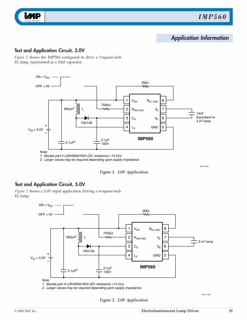
Figure 1. 3.0V Application
Test and Application Circuit, 3.0VFigure 1 shows the IMP560 configured to drive a 3-square-inch EL lamp, represented as a 10nF capacitor.
+
–
ON = VDD
OFF = 0V
VDD
RSW-OSC
CS
LX
REL-OSC
VA
VB
GND
8
7
6
5
1
2
3
4
IMP560
2MΩ
750kΩ560µH1
VIN = 5.0V
0.1µF2
L
1N4148
6 in2 lamp
Note:1. Murata part # LQH4N561K04 (DC resistance <14.5 Ω)2. Larger values may be required depending upon supply impedance.
560_10.eps
0.1µF100V
Figure 2. 5.0V Application
Test and Application Circuit, 5.0VFigure 2 shows a 5.0V input application driving a 6-square-inch EL lamp.
Application Information

I M P 5 6 0I M P 5 6 0
30 408-432-9100/www.impweb.com © 2000 IMP, Inc. !
Enable/Disable OperationFigure 3 shows the IMP560 can be enabled via a logic gate that con-nects RSW to VDD, and disabled by connecting it to ground. RELmaybe connected either to VDD or to the gate.
RSW Connection IMP560 StateVDD Enabled
Ground Disabled
Figure 3. Enable/Disable Operation
+
–
ON = VDD
OFF = 0V
VDD
RSW-OSC
CS
LX
REL-OSC
VA
VB
GND
8
7
6
5
1
2
3
4
IMP560
REL
CMOSGate
RSWL1
VIN
0.1µF2
15V
1N4148
EL lamp
Note:1. Murata part # LQH4N561K04 (DC resistance <14.5 Ω)2. Larger values may be required depending upon supply impedance.
560_11.eps
0.1µF100V
Enable/Disable Table
Dual Supply Operation with 1.5V BatteryThe IMP560 can also be operate from a single battery cell when aregulated voltage higher than 2.0V is also available. The dualsupply configuration, shown in Figure 4, uses the regulated voltage to operate the IMP560 while the energy for the high-voltage boost circuit comes from the battery. The current to runthe internal logic is typically 420µA.
The circuit of Figure 4 can also be used with batteries that exceed6.0V as long as VDD does not exceed 6.5V.
+
–
VDD
RSW-OSC
CS
LX
REL-OSC
VA
VB
GND
8
7
6
5
1
2
3
4
IMP560
REL
Regulated Voltage(2.0V to 6.5V)
RSWL
BatteryVoltage
VIN
0.1µF*
1N4148
EL lamp
560_12.eps
0.1µF100V
CS
* Larger values may be requireddepending upon supply impedance
ON = VDD
OFF = 0V
Figure 4. Dual Supply Operation with High Battery Voltages
© 2000 IMP, Inc. 408-432-9100/www.impweb.com 31
IMP803IMP803POWER MANAGEMENT
High-High-VVoltoltagage EL Lame EL Lamp Drp Driviverer
GPS units/Pagers/Cellular phones PDAs/Handheld computers Safety illumination Portable instrumentation Battery-operated displays LCD modules Toys
Low Power: 420µA typical VDD current Wide operating voltage range - from 2.0V to 6.5V 180V peak-to-peak typical AC output voltage Large output load capability - drive lamps
with more than 30nF capacitance Adjustable output lamp frequency for control of
lamp color, lamp life, and power consumption Adjustable converter frequency to minimize
power consumption Device can be Enabled/Disabled Low quiescent current – 20nA (disabled) High-Voltage CMOS Process MicroSO package option
Key Features
Applications
–
+
803_01.eps
VDD1
LX4
CS3
VA7
VB6
RSW-OSC2 Switch
Oscillator
RegulationControl
IMP803 BridgeOutputDriver
Q
Q
Q
VREF
Lamp DriveOscillator
C
GND5
REL-OSC8
Q
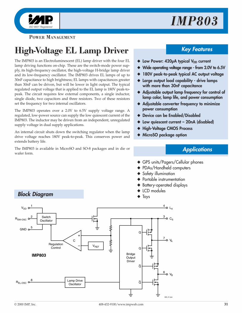
The IMP803 is an Electroluminescent (EL) lamp driver with the four ELlamp driving functions on-chip. These are the switch-mode power sup-ply, its high-frequency oscillator, the high-voltage H-bridge lamp driverand its low-frequency oscillator. The IMP803 drives EL lamps of up to30nF capacitance to high brightness; EL lamps with capacitances greaterthan 30nF can be driven, but will be lower in light output. The typicalregulated output voltage that is applied to the EL lamp is 180V peak-to-peak. The circuit requires few external components, a single inductor,single diode, two capacitors and three resistors. Two of these resistors set the frequency for two internal oscillators.
The IMP803 operates over a 2.0V to 6.5V supply voltage range. Aregulated, low-power source can supply the low quiescent current of theIMP803. The inductor may be driven from an independent, unregulatedsupply voltage in dual supply applications.
An internal circuit shuts down the switching regulator when the lampdrive voltage reaches 180V peak-to-peak. This conserves power andextends battery life.
The IMP803 is available in MicroSO and SO-8 packages and in die orwafer form.
Block Diagram

I M P 8 0 3I M P 8 0 3
32 408-432-9100/www.impweb.com © 2000 IMP, Inc.
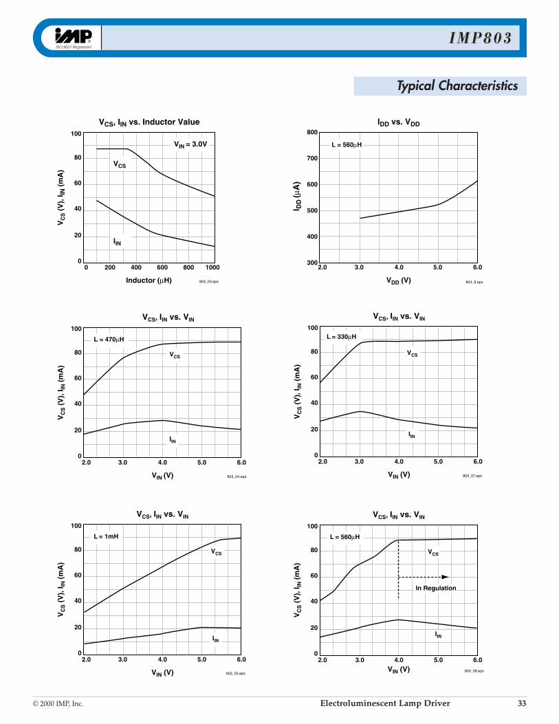
Parameter Symbol Conditions Min Typ Max UnitsON-resistance of MOS Switch RDS(ON) I = 100mA 3.5 8 ΩOutput Voltage Regulation VCS VDD = 2.0 to 6.5V 80 90 100 VOutput Voltage Peak-to-peak (in regulation) VA-VB VDD = 2.0 to 6.5V 160 180 200 VQuiescent VDD Supply Current, Disabled IDDQ VRSW-OSC <100mV 20 200 nAInput Current at VDD Pin IDD VDD = 3.0V, See Figure 1 420 700 µAInput Current at VDD Pin IDD VDD = 5.0V, See Figure 2 500 750 µAInput Current: IDD Plus Inductor Current IIN VDD = 3.0V, See Figure 1 20 31 mAOutput Voltage at VCS VCS VDD = 3.0V, See Figure 1 60 74 100 VVA-B Output Drive Frequency fEL VDD = 3.0V, See Figure 1 300 370 430 HzSwitching Frequency fSW VDD = 3.0V, See Figure 1 50 70 90 kHzSwitching Duty Cycle DSW VDD = 3.0V, See Figure 1 88 %
4LX
3CS
2RSW-OSC
1VDD
5 GND
6 VB
7 VA
8 REL-OSC
803_02.eps
IMP803
SO/ MicroSO
Part Number Input Voltage Regulated Output Voltage Temperature Range Pins-Package IMP803LG 2.0V to 6.5V Yes –40°C to +85°C 8-SO
IMP803IMA 2.0V to 6.5V Yes –40°C to +85°C 8-MicroSO
IMP803SX* 2.0V to 6.5V Yes 25°C Dice
IMP803/D1** 2.0V to 6.5V Yes 25°C Dice
VDD, VRSW-OSC and VREL-OSC . . . . . . . . . . . . . . . –0.5V to +7.0VVCS, LX . . . . . . . . . . . . . . . . . . . . . . . . . . . . . . . . –0.5V to +120VOperating Temperature Range . . . . . . . . . . . . –40°C to +85°CStorage Temperature Range . . . . . . . . . . . . . . –65°C to +150°CPower Dissipation (SO) . . . . . . . . . . . . . . . . . . 400mWPower Dissipation (MicroSO) . . . . . . . . . . . . . 300mWVA, VB . . . . . . . . . . . . . . . . . . . . . . . . . . . . . . . . –0.5V to VCS (pin 3)
Unless otherwise noted, VDD = 3.0V, RSW = 750kΩ, REL = 2.0MΩ, and TA = 25°C.
Note: All voltages are referenced to GND.
These are stress ratings only and functional operation is notimplied. Exposure to absolute maximum ratings for prolongedtime periods may affect device reliability.
Pin Compatible With HV803 and IMP560
Ordering Information
Pin Configuration
Absolute Maximum Ratings
Electrical Characteristics
* Disable pad not active** Disable pad active
Add /T to ordering part number for Tape and Reel.
I M P 8 0 3I M P 8 0 3
© 2000 IMP, Inc. Electroluminescent Lamp Driver 33
0
VC
S (
V),
I IN
(m
A)
Inductor (µH) 803_03.eps
100
80
60
40
20
0
VCS, IIN vs. Inductor Value
200 600 800400 1000
VIN = 3.0V
VCS
IIN
2.0
I DD
(µA
)
VDD (V)
800
700
600
500
400
300
IDD vs. VDD
3.0 4.0 5.0 6.0
803_6.eps
L = 560µH
2.0
VC
S (
V),
I IN (
mA
)
VIN (V)
100
80
60
40
20
0
VCS, IIN vs. VIN
3.0 4.0 5.0 6.0
L = 330µH
VCS
IIN
803_07.eps
2.0
VC
S (
V),
I IN (
mA
)
VIN (V)
100
80
60
40
20
0
VCS, IIN vs. VIN
3.0 4.0 5.0 6.0
L = 470µH
VCS
IIN
803_04.eps
2.0
VC
S (
V),
I IN (
mA
)
VIN (V)
100
80
60
40
20
0
VCS, IIN vs. VIN
3.0 4.0 5.0 6.0
L = 1mH
VCS
IIN
803_05.eps
2.0
VC
S (
V),
I IN (
mA
)
VIN (V)
100
80
60
40
20
0
VCS, IIN vs. VIN
3.0 4.0 5.0 6.0
L = 560µH
VCS
In Regulation
IIN
803_08.eps
Typical Characteristics

I M P 8 0 3I M P 8 0 3
34 408-432-9100/www.impweb.com © 2000 IMP, Inc. !
Pin Descriptions
External Components
Pin Number Name Function1 VDD Positive voltage supply for the IMP803. Inductor L may be connected here or to a
separate unregulated supply.
2 RSW-OSC Switch-mode resistor pin. Switching frequency is determined by an external resistor, RSW.
3 CS Boost converter storage capacitor. The voltage across the EL lamp is equal to twice the voltage at CS.
4 LX Connection to flyback inductance, L.
5 GND Ground pin.
6 VB EL lamp drive. The lamp is connected in a high-voltage bridge circuit with VB providing the complementary connection to VA. The peak-to-peak AC voltage across the EL lamp is thus two times VCS.
7 VA EL lamp drive. (See above)
8 REL-OSC The EL lamp oscillator frequency setting pin. The oscillator frequency is controlled by external resistor REL.
External Component Description and Selection GuideDiode Catch diode. A fast reverse recovery diode, with BV > 100, such as a 1N4148.
Capacitor CS This is the high voltage capacitor that stores the inductive energy transferred through the catch diode. A 100 volt capacitor between 10nF and 100nF is recommended.
Resistor REL The EL lamp oscillator frequency setting resistor. This resistor, connected between the REL-OSC pin and VDD, provides an oscillator frequency inversely proportional to REL; as REL increases, the EL lamp frequency decreases along with the current drawn by the lamp. Lamp color is also determined by this frequency. A 2MΩ resistor between the REL-OSC pin and the VDD supply results in a lamp frequency around 350Hz: a 1MΩ resistor will give ≈700Hz.
Resistor RSW Switching Oscillator frequency setting resistor. The switching oscillator resistor is connected between the RSW-OSC pin and the VDD supply. The switching frequency is inversely proportionalto the resistor value, dropping as the resistance increases.
Inductor L The inductor provides the voltage boost needed by means of inductive “flyback”. The internalMOSFET switch alternately opens and closes the ground connection for the inductor at the LX pin. When this internal switch opens, the inductor potential will forward-bias the catch diode and the current will pass through the storage capacitor CS, charging it to a high voltage.
Smaller inductors are preferred to prevent saturation. As the value of the inductor increases (and the series DC resistance of the inductor decreases), the switching frequency set by RSW should be increased to prevent saturation. In general, smaller value inductors thatcan handle more current are more desirable when larger area EL lamps must be driven.
Lamp, RCL An external resistor (RCL) in series with the lamp will protect the output drivers from high transient currents during lamp commutation.
The IMP803 generates high voltages and caution should be exercised.
High Voltages Present

I M P 8 0 3I M P 8 0 3
© 2000 IMP, Inc. Electroluminescent Lamp Driver 35
+
–
VDD
RSW-OSC
CS
LX
REL-OSC
VA
VB
GND
8
7
6
5
1
2
3
4
IMP803
2kΩ
2MΩ
REL
750kΩ560µH1
VIN = 3.0V
0.1µF2
1N4148
L10nFEquivalent to3 in2 lamp
Note:1. Murata part # LQH4N561K04 (DC resistance <14.5 Ω)2. Larger values may be required depending upon supply impedance.
RCL
803_09.eps
ON = VDD
OFF = 0V
0.1µF100V
RSW
CS
Figure 1. 3.0V Application
Test and Application Circuit, 3.0VFigure 1 shows the IMP803 configured to drive a 3-square-inch EL lamp, represented as a 10nF capacitor. With a 3.0V input, theEL lamp will be driven to moderate brightness.
+
–
VDD
RSW-OSC
CS
LX
REL-OSC
VA
VB
GND
8
7
6
5
1
2
3
4
IMP803
2kΩ
2MΩ
REL
750kΩ560µH1
VIN = 5.0V
0.1µF2 CS
1N4148
6 in2 lamp
Note:1. Murata part # LQH4N561K04 (DC resistance <14.5 Ω)2. Larger values may be required depending upon supply impedance.
RCL
803_10.eps
0.1µF100V
ON = VDD
OFF = 0V
RSW
L
Figure 2. 5.0V Application
Test and Application Circuit, 5.0VFigure 2 shows a 5.0V input application driving a 6-square-inch EL lamp.
Application Information

I M P 8 0 3I M P 8 0 3
36 408-432-9100/www.impweb.com © 2000 IMP, Inc. !
+
–
VDD
RSW-OSC
CS
LX
REL-OSC
VA
VB
GND
8
7
6
5
1
2
3
4
IMP803
2kΩ
2MΩ
REL
330kΩ560µH1
VIN = 6.0V
0.1µF2
1N4148
10 in2 lamp
Note:1. Murata part # LQH4N561K04 (DC resistance <14.5 Ω)2. Larger values may be required depending upon supply impedance.
RCL
803_11.eps
0.1µF100V
LRSW
CS
Enable/Disable OperationFigure 4 shows that the IMP803 can be enabled via a logic gate thatconnects RSW to VDD, and disabled by connecting it to ground.
RSW Connection IMP803 StateVDD Enabled
GND Disabled
Figure 3. 6.0V Application
Figure 4. Enable/Disable Operation
+
–
ON = VDD
OFF = 0V
VDD
RSW-OSC
CS
LX
REL-OSC
VA
VB
GND
8
7
6
5
1
2
3
4
IMP803
RCL
REL
CMOSGate
RSWL1
VIN
0.1µF2
1N4148
EL lamp
Note:1. Murata part # LQH4N561K04 (DC resistance <14.5 Ω)2. Larger values may be required depending upon supply impedance. 803_12.eps
0.1µF100VCS
Test and Application Circut, 6.0VAt higher input voltage levels, the IMP803 will drive large ELlamps. Figure 3 shows a 6.0V circuit configuration that will drivea 10 square-inch lamp.
Enable/Disable Table
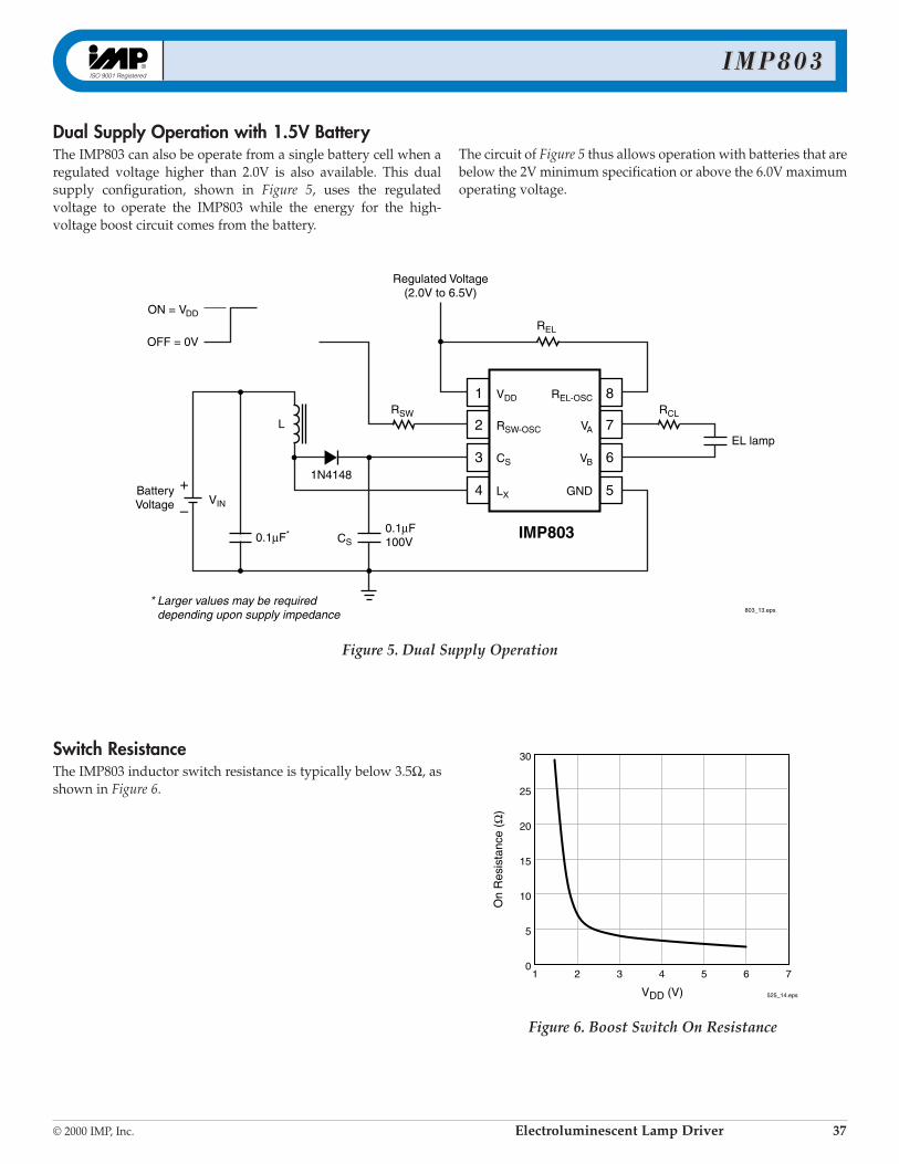
I M P 8 0 3I M P 8 0 3
© 2000 IMP, Inc. Electroluminescent Lamp Driver 37
Dual Supply Operation with 1.5V BatteryThe IMP803 can also be operate from a single battery cell when aregulated voltage higher than 2.0V is also available. This dualsupply configuration, shown in Figure 5, uses the regulated voltage to operate the IMP803 while the energy for the high-voltage boost circuit comes from the battery.
The circuit of Figure 5 thus allows operation with batteries that arebelow the 2V minimum specification or above the 6.0V maximumoperating voltage.
+
–
VDD
RSW-OSC
CS
LX
REL-OSC
VA
VB
GND
8
7
6
5
1
2
3
4
IMP803
RCL
REL
Regulated Voltage(2.0V to 6.5V)
RSW
VIN
L
BatteryVoltage
0.1µF*
1N4148
EL lamp
803_13.eps* Larger values may be required
depending upon supply impedance
ON = VDD
OFF = 0V
0.1µF100VCS
Figure 5. Dual Supply Operation
Switch ResistanceThe IMP803 inductor switch resistance is typically below 3.5Ω, asshown in Figure 6.
On
Res
ista
nce
(Ω)
VDD (V) 525_14.eps
1 2 3 4 5 6 70
5
10
15
20
25
30
Figure 6. Boost Switch On Resistance

38 408-432-9100/www.impweb.com © 2000 IMP, Inc. !
Notes
Project

© 2000 IMP, Inc. Electroluminescent Lamp Driver 39
IMP525 - Die Specif ications
Pad Number Name Function
1 VDD Positive voltage supply.
2 RSW-OSC Switch-mode oscillator frequency setting pad.
3 CS Boost converter storage capacitor pad.
4 LX Inductor pad.
5 GND Ground pad.
6 VB EL lamp drive.
7 VA EL lamp drive.
8 REL-OSC EL lamp oscillator frequency setting pad.
9* DIS Disable pad. DIS = HIGH disables chip.
IMP525Single Cell Battery Powered EL Lamp Driver
Die Thickness: 25 mils (625 microns)
Bond Wire Size: 1.0 mil (25 microns)
Back Side Metal: None
Back Side Potential: Ground
Die Attach Method: Conductive Adhesive
Bond Pad Metal: Aluminum, 1% Silicon, 1/2% Copper
Bond Pad Size: 100 microns per side
Die Size: 1.35mm x 1.54mm
General Information Pad Description
Pad Number X (microns) Y (microns)
1 1153 1092
2 476 1226
3 314 1226
4 143 1216
5 111 460
6 397 112
7 1104 112
8 1153 958
9 1153 1226
Pad Location1
Notes 1. To bonding pad center
5GND
4 3 2
LX CSRSW-OSC
19 DIS
VDD8 REL-OSC
76
VAVB
1.35mm
1.54mm
(0, 0)
IMP525
Ordering Information
traPrebmuN
daPrebmuN
noitpircseD
daPelbasiDevitcA
daPelbasiDevitcAtoN
D/525PMI 9
1D/525PMI 9
10t_eiD525
* See Ordering Information table

IMP527 - Die Specif ications
40 408-432-9100/www.impweb.com © 2000 IMP, Inc. !
Pad Number Name Function
1 VDD Positive voltage supply.
2 RSW-OSC Switch-mode oscillator frequency setting pad.
3 CS Boost converter storage capacitor pad.
4 LX Inductor pad.
5 GND Ground pad.
6 VB EL lamp drive.
7 VA EL lamp drive.
8 REL-OSC EL lamp oscillator frequency setting pad.
9* DIS Disable pad. DIS = HIGH disables chip.
IMP527Single Cell Battery Powered EL Lamp Driver, 180VPP Drive
Die Thickness: 25 mils (625 microns)
Bond Wire Size: 1.0 mil (25 microns)
Back Side Metal: None
Back Side Potential: Ground
Die Attach Method: Conductive Adhesive
Bond Pad Metal: Aluminum, 1% Silicon, 1/2% Copper
Bond Pad Size: 100 microns per side
Die Size: 1.35mm x 1.54mm
General Information Pad Description
Pad Number X (microns) Y (microns)
1 1153 1092
2 476 1226
3 314 1226
4 143 1216
5 111 460
6 397 112
7 1104 112
8 1153 958
9 1153 1226
Pad Location1
Notes 1. To bonding pad center
5GND
4 3 2
LX CSRSW-OSC
19 DIS
VDD8 REL-OSC
76
VAVB
1.35mm
1.54mm
(0, 0)
IMP527
Ordering Information
traPrebmuN
elbasiDdaP
rebmuN
noitpircseD
daPelbasiDevitcA
daPelbasiDevitcAtoN
D/725PMI 9
1D/725PMI 9
10t_eiD725
* See Ordering Information table
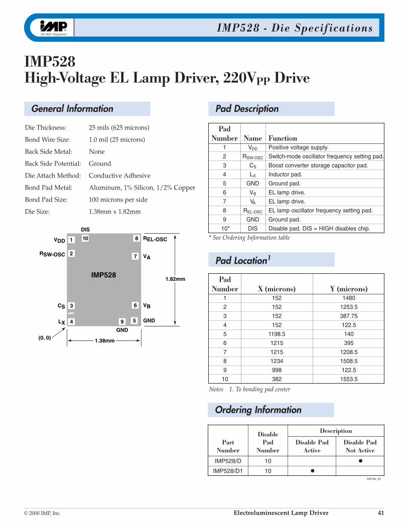
© 2000 IMP, Inc. Electroluminescent Lamp Driver 41
IMP528 - Die Specif ications
Pad Number Name Function
1 VDD Positive voltage supply.
2 RSW-OSC Switch-mode oscillator frequency setting pad.
3 CS Boost converter storage capacitor pad.
4 LX Inductor pad.
5 GND Ground pad.
6 VB EL lamp drive.
7 VA EL lamp drive.
8 REL-OSC EL lamp oscillator frequency setting pad.
9 GND Ground pad.
10* DIS Disable pad. DIS = HIGH disables chip.
IMP528High-Voltage EL Lamp Driver, 220VPP Drive
Die Thickness: 25 mils (625 microns)
Bond Wire Size: 1.0 mil (25 microns)
Back Side Metal: None
Back Side Potential: Ground
Die Attach Method: Conductive Adhesive
Bond Pad Metal: Aluminum, 1% Silicon, 1/2% Copper
Bond Pad Size: 100 microns per side
Die Size: 1.38mm x 1.82mm
General Information Pad Description
Pad Number X (microns) Y (microns)
1 152 1480
2 152 1253.5
3 152 387.75
4 152 122.5
5 1198.5 140
6 1215 395
7 1215 1208.5
8 1234 1508.5
9 998 122.5
10 382 1553.5
Pad Location1
Notes 1. To bonding pad center
1 10
2
3
4
VDD
RSW-OSC
CS
LX
(0, 0)
9
GND
5
6
7
8
GND
VB
VA
REL-OSC
DIS
IMP528
1.38mm
1.82mm
Ordering Information
traPrebmuN
elbasiDdaP
rebmuN
noitpircseD
daPelbasiDevitcA
daPelbasiDevitcAtoN
D/825PMI 01
1D/825PMI 01
10t_eiD825
* See Ordering Information table

IMP560 - Die Specif ications
42 408-432-9100/www.impweb.com © 2000 IMP, Inc. !
Pad Number Name Function
1 VDD Positive voltage supply.
2 RSW-OSC Switch-mode oscillator frequency setting pad.
3 CS Boost converter storage capacitor pad.
4 LX Inductor pad.
5 GND Ground pad.
6 VB EL lamp drive.
7 VA EL lamp drive.
8 REL-OSC EL lamp oscillator frequency setting pad.
9 GND Ground pad.
10* DIS Disable pad. DIS = HIGH disables chip.
IMP560Power Efficient EL Lamp Driver
Die Thickness: 25 mils (625 microns)
Bond Wire Size: 1.0 mil (25 microns)
Back Side Metal: None
Back Side Potential: Ground
Die Attach Method: Conductive Adhesive
Bond Pad Metal: Aluminum, 1% Silicon, 1/2% Copper
Bond Pad Size: 100 microns per side
Die Size: 1.38mm x 1.82mm
General Information Pad Description
Pad Number X (microns) Y (microns)
1 152 1480
2 152 1253.5
3 152 387.75
4 152 122.5
5 1198.5 140
6 1215 395
7 1215 1208.5
8 1234 1508.5
9 998 122.5
10 382 1553.5
Pad Location1
Notes 1. To bonding pad center
1 10
2
3
4
VDD
RSW-OSC
CS
LX
(0, 0)
9
GND
5
6
7
8
GND
VB
VA
REL-OSC
DIS
IMP560
1.38mm
1.82mm
Ordering Information
traPrebmuN
daPrebmuN
noitpircseD
daPelbasiDevitcA
daPelbasiDevitcAtoN
D/065PMI 01
1D/065PMI 01
10t_eiD065
* See Ordering Information table
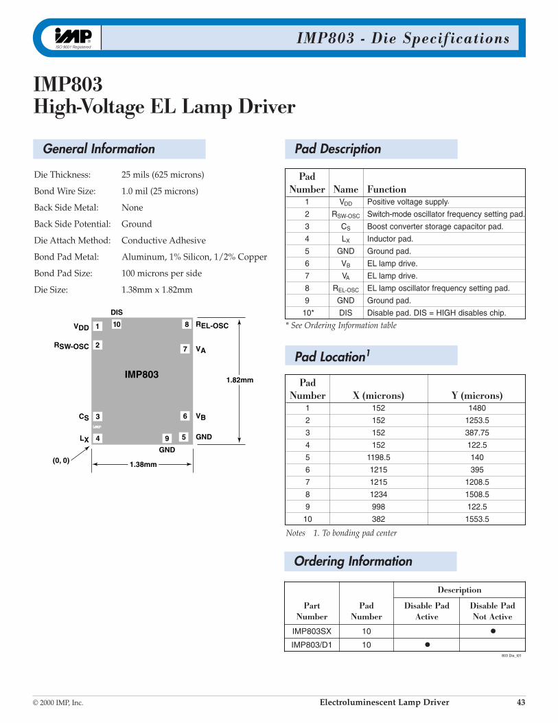
© 2000 IMP, Inc. Electroluminescent Lamp Driver 43
IMP803 - Die Specif ications
Pad Number Name Function
1 VDD Positive voltage supply.
2 RSW-OSC Switch-mode oscillator frequency setting pad.
3 CS Boost converter storage capacitor pad.
4 LX Inductor pad.
5 GND Ground pad.
6 VB EL lamp drive.
7 VA EL lamp drive.
8 REL-OSC EL lamp oscillator frequency setting pad.
9 GND Ground pad.
10* DIS Disable pad. DIS = HIGH disables chip.
IMP803High-Voltage EL Lamp Driver
Die Thickness: 25 mils (625 microns)
Bond Wire Size: 1.0 mil (25 microns)
Back Side Metal: None
Back Side Potential: Ground
Die Attach Method: Conductive Adhesive
Bond Pad Metal: Aluminum, 1% Silicon, 1/2% Copper
Bond Pad Size: 100 microns per side
Die Size: 1.38mm x 1.82mm
General Information Pad Description
Pad Number X (microns) Y (microns)
1 152 1480
2 152 1253.5
3 152 387.75
4 152 122.5
5 1198.5 140
6 1215 395
7 1215 1208.5
8 1234 1508.5
9 998 122.5
10 382 1553.5
Pad Location1
Notes 1. To bonding pad center
1 10
2
3
4
VDD
RSW-OSC
CS
LX
(0, 0)
9
GND
5
6
7
8
GND
VB
VA
REL-OSC
DIS
IMP803
1.38mm
1.82mm
Ordering Information
traPrebmuN
daPrebmuN
noitpircseD
daPelbasiDevitcA
daPelbasiDevitcAtoN
XS308PMI 01
1D/308PMI 01
10t_eiD308
* See Ordering Information table
44 408-432-9100/www.impweb.com © 2000 IMP, Inc. !
Notes
Project

© 2000 IMP, Inc. 408-432-9100/www.impweb.com 45
Application Note 1POWER MANAGEMENT ELECTROLUMINESCENT LAMP DRIVER
Electroluminescent Lamp Driver Evaluation Board
Introduction
Figure 1. Circuitry in gray is on-chip.
This Application Note introduces an Evaluation Board for IMP ELdriver ICs. It is supplied with the IMP803 but can also be usedwith the IMP560 and IMP525: all 3 have identical pinouts.
EL Lamps and DriversAn electroluminescent (EL) lamp consists of a phosphor coatingon a dielectric that is sandwiched between two conductors.Electrically, it looks like a capacitor. Such a lamp requires drivefrom a high alternating voltage source in order to emit light. Thiscan be obtained from IMP integrated circuits IMP803, IMP560 andIMP525 that convert low voltages into appropriate high-voltagewaveforms.
Small EL lamps exhibit about 2 to 6nF/in2. IMP Driver ICs arecapable of powering EL lamps that have total equivalent loadcapacitances up to 30nF, so this works out to a maximum ofaround 15 square inches. “Powering” in this context meansenabling enough light for the application, which can range fromLCD backlights (relatively bright in a handheld device) to pagers(medium-bright, in a poorly-lit room), to night-lights (faint, in adark room).
IMP Driver IC System DiagramAs shown in Figure 1, these ICs contain a high-voltage MOSFETswitch, an output H-bridge, and oscillators to drive each. Theswitch, combined with an external inductor and diode, form astep-up (boost) converter that transforms the input voltage to 45-90 volts across capacitor CS. This, in turn, is switched from oneside of the load (the EL lamp) to the other by a commutatingbridge, driven by its own oscillator. This action causes the lamp toexperience twice the CS value (i.e. 90-180 volts peak-to-peak) withno DC component.
A typical application uses a switch frequency of 80kHz and bridgecommutation frequency of 360Hz. These frequencies are control-lable via external resistors; RSW for the boost converter and REL forthe output driver. REL influences brightness, color and EL lamplife. RSW controls converter efficiency. Both affect power con-sumption.
RELRSW
CBATT
GND
VDD
VA VB+
–
D1L1
CS
LAMP
IMP Driver IC System Diagram
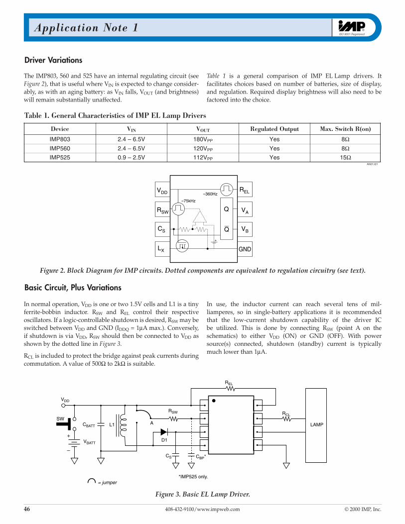
Application Note 1
46 408-432-9100/www.impweb.com © 2000 IMP, Inc. !
Figure 3. Basic EL Lamp Driver.
Figure 2. Block Diagram for IMP circuits. Dotted components are equivalent to regulation circuitry (see text).
In normal operation, VDD is one or two 1.5V cells and L1 is a tiny ferrite-bobbin inductor. RSW and REL control their respective oscillators. If a logic-controllable shutdown is desired, RSW may beswitched between VDD and GND (IDDQ = 1µA max.). Conversely,if shutdown is via VDD, RSW should then be connected to VDD asshown by the dotted line in Figure 3.
RCL is included to protect the bridge against peak currents duringcommutation. A value of 500Ω to 2kΩ is suitable.
In use, the inductor current can reach several tens of mil-liamperes, so in single-battery applications it is recommendedthat the low-current shutdown capability of the driver IC be utilized. This is done by connecting RSW (point A on theschematics) to either VDD (ON) or GND (OFF). With powersource(s) connected, shutdown (standby) current is typicallymuch lower than 1µA.
Basic Circuit, Plus Variations
The IMP803, 560 and 525 have an internal regulating circuit (seeFigure 2), that is useful where VIN is expected to change consider-ably, as with an aging battery: as VIN falls, VOUT (and brightness)will remain substantially unaffected.
Table 1 is a general comparison of IMP EL Lamp drivers. It facilitates choices based on number of batteries, size of display,and regulation. Required display brightness will also need to befactored into the choice.
Table 1. General Characteristics of IMP EL Lamp Drivers
RCL
REL
RSW
AL1
+
–
CBATT
VBATT
SW
VDD
D1
LAMP
= jumper
CS CBP*
*IMP525 only.
VDD
RSW
CS
LX
REL
VAQ
≈360Hz
≈75kHz
Q VB
GND
+
Driver Variations
eciveD V NI V TUO tuptuOdetalugeR )no(RhctiwS.xaM
308PMI V5.6–4.2 V081 PP seY 8Ω065PMI V5.6–4.2 V021 PP seY 8Ω525PMI V5.2–9.0 V211 PP seY 51 Ω
10t.10NA
Application Note 1
© 2000 IMP, Inc. Electroluminescent Lamp Driver 47
Using the circuit in Figure 5, one can utilize an available VIN thatis higher or lower than the allowable VDD. The logic shutdownmay also be separated from VDD. Such arrangements are helpfulwhen the inductor supply is too low for the IC, or the display sizerequires a voltage that is too high for the IC.
A higher VIN will need a higher switching frequency to keep theinductor out of saturation. In all cases, note the presence of HIGHVOLTAGE!
Having said that keeping RCL is a good idea, it is true that remov-ing as many components as possible may also be desirable. Forthe IMP803, REL and RSW may be combined as shown in Figure 4.Varying REL causes a visible change in brightness and color, but asimilar variation in RSW (affecting oscillator frequency and powerconsumption) is much less noticeable. Combining the two is thus
a valid way to save a resistor. The bypass capacitor CBP (IMP525only) reduces display flicker in noisy environments, such as whenthere is no ground plane.
Figure 4. Using RSW to supply current for both switch and EL oscillators, and also serve as a low-current on/off switch(IMP803 only).
Figure 5. General Circuit, where chip VDD, on/off logic and VIN are all different.
Reducing Component Count
RCLRSW
AL1CBATT
VDD
D1
CS
LAMP
= jumper
RCL
REL
ON –
OFF
RSW
L1CBATT
VIN VDD
D1
CS CBP*
*IMP525 only.
LAMP
+
–
VBATT
Application Note 1
48 408-432-9100/www.impweb.com © 2000 IMP, Inc. !
Evaluation BoardThe ELD002 is a PC board for evaluation and experimentationpurposes. More compact arrangements are easily achieved byusing surface-mounted components exclusively. The various pos-sible connections mirror the options discussed in the data sheetand the Application Note.
The two dark patches are the connections for the EL lamp whichare made using conductive double-sided tape. The display itself isheld down with ordinary double-sided tape. Taping is advanta-geous for several reasons, among which are that lamps with
staked connecting terminals generally cost more, and they are apossible site for mechanical (and thus electrical) failure.
As a general precaution, note that HIGH VOLTAGE exists on theboard; around 180V or so. The current level is low so there is nodanger, except possible pain if a tender skin area or open cut con-tacts the HV sections.
There are extra holes for capacitors (if needed), and the hole spac-ings are wide enough to accommodate 1/4W resistors. Cornermounting holes have also been provided.
RCL
REL
VA
VB
GND
VDD
RSW
CS
LX
REL
RSW
L1
A
GND
JP1
= jumper: RSW and L1 are normally connected to VDD.
VDD
VDD
VIND1
CBP
LAMP
CIN CS
CBATT
+
–
VBATT
SWSW
Figure 6. Evaluation Board Layout and Schematic.
RSW
DI
VDD
GND
A
U1
L1CIN
CBATT
CS
DISPLAY
SW BAT
REL
JP1
RC
L
GN
D
VD
D
LAM
PO
UT
EL
Driv
er B
oard
EL
D00
2
Cbp
ISO
900
1 R
egis
tere
d®
Application Note 1
© 2000 IMP, Inc. Electroluminescent Lamp Driver 49
Additional Points1) To experiment with the Figure 4 scheme, a jumper may be run from the rightmost pad of REL to the leftmost pad of CBP (with
the + above it). Start with an RSW of 750kΩ. Short leads and a ground plane are more critical in this arrangement.
2) CS should be 10nF - 100nF.
3) The IMP803, IMP560 and IMP525 datasheets show performance with different inductors. For example, high-voltage regulation isreached earlier with lower L, but this requires more current. This may be partially offset by adjustment of the oscillator resistors.
4) To experiment with multiple supplies, the appropriate jumpers may be removed.
5) The inclusion of RCL should be stressed: while 500Ω to 10kΩ has been used, 2kΩ is the best all-around value.
Layout Rules for Other Arrangements1) A ground plane is recommended to keep stray high frequencies confined. In a very small area, the need for a ground
plane may be nil. A totally surface-mount arrangement would make such a plane difficult anyway.
2) Locate high voltages away from the high-impedance elements REL and RSW.
3) Make sure that CS has a rating of at least 100V.
4) The diode should have good reverse-recovery characteristics (the general-purpose 1N4148 is adequate) and should be rated for pulsed BV > 100V for the IMP803, and pulsed BV > 75V for the IMP560 and IMP525.
5) Shutdown by a logic-level signal is possible by connecting RSW to ground (RSW is normally connected to VDD). This on/off logicuses only 1µA max. when connected at this location.
7) Required voltage ratings for the capacitors other than CS are flexible, and need only reflect actual stresses plus a safety margin.
To keep the board light in weight, a Li-Mn power source wasselected. When energized, the drain from the circuit is around22mA, thus the CR battery chemistry is preferred over the BR forits superior pulse performance. If long-term continual illumina-tion is anticipated and space is not an issue, alkaline batteries maybe more economical.
With the IMP803 and 560µH inductor supplied, regulation beginsat about 3-3.5V, but display illumination appears virtually
unchanged above 2.7V. When choosing the battery chemistry, it isa good idea to match the cell “plateau” voltages to this. For exam-ple, a typical NiCad plateau is 1.2V under load, so more than 2cells would be needed. Alkaline plateaus are somewhat higher,and they differ with size, shape and duty, so 2 cells could suffice.Li-Mn coin cells have their voltage plateau under load at about2.85 volts. They can drop lower, but they also return to close to 3Vwhen the load is removed.
Some Battery Considerations

Application Note 1
50 408-432-9100/www.impweb.com © 2000 IMP, Inc. !
Key to Components and Ratings
Bill of Materials
Component Value Function CommentsRSW 30kΩ to 3MΩ Sets switch osc. frequency. Decrease R to increase frequency.
REL 500kΩ to 10MΩ Sets bridge osc. frequency. Decrease R to increase frequency.
RCL 500Ω to 2kΩ Limits output current. Protects IC.
CS 0.01µF to 0.1µF, 100V Stores high voltage. Use low values for large lamps.
CBATT 0.1µF, 10V Supply bypass. Keeps supply impedance low.
CBP 1nF, 10V Lowers noise at RSW. IMP525 only.
CIN 0.1µF to 22µF Supply bypass. Keeps supply impedance low.
L1 100µH to 1mH Stores energy. Small L, high f increases VOUT.
D1 100V, 10mA (1N4148) Passes energy from L to CS. Use fast recovery type.
Component Description Manufacturer Part NumberResistors (±5%) See Table, below
Capacitors (±20%) See Table, below Murata RPE121/122 Series
Switch SPST, momentary Panasonic P8008S
Battery 3.0V Li-Mn Coin Sony CR2450-HE4Panasonic CR2354-IGU
Inductor L1 = 560µH Murata LQH4N561K04
Diode D1 = 1N4148
Lamp 1.3” x 2.05” MetroMark or other
Conductive Tape Connects display Adhesives Research ARclad 8001
Double-Sided Tape Holds display down 3M Type 665
APPENDIX: Introduction to EL LampsChemical compounds, called phosphors, glow when energy is applied to them. This excitation energy can come from conducted orradiated electrons, or an electric field. A common example of this process is found in the emitted (radiated) electrons that impinge onthe dots and stripes of color monitors and TVs, whose phosphors emit everything from pure colors to white light, depending on theirformulations.
Backlights and lamps generally are simpler, employing a manganese-activated zinc sulfide phosphor (ZnS:Mn) that is excited by ahigh-voltage (> 40V) AC electric field (DC can shorten the lamp life). Fabrication involves depositing the phosphor as a thin film ontoa BaTiO3 dielectric between conducting planes, like a capacitor: one of the planes is the transparent conductor, indium tin oxide (ITO).The lamp color depends on phosphor formulation, but also on its physical realization (i.e. encapsulation, resins, dyes, etc.), plus thecharacteristics of the drive circuitry.
The IMP line of drivers is targeted mainly at applications like backlight EL and stand-alone pre-printed or segmented lamps. Backlightsare used with the Liquid Crystal Displays (LCDs) found in cellular telephones, pagers, Personal Digital Assistants (PDAs), and general-purpose local lighting applications where low power consumption without heat is important (e.g. airline cockpits, medical instrumenta-tion).
The excitation required for lamps ranges from tens to hundreds of volts, at frequencies from 60Hz to a few kHz. Each display has anoptimum combination depending on size, color, efficiency and desired brightness.
In general, the changes in brightness with frequency and voltage are nearly linear. These facts allow tradeoffs. For example, if goingabove a certain voltage is not allowed, an increase in drive frequency may achieve the same result.

© 2000 IMP, Inc. 408-432-9100/www.impweb.com 51
Application Note 4POWER MANAGEMENT ELECTROLUMINESCENT LAMP DRIVER
Introduction
EL Driver Demonstration PC Boards,IMP-DBM and IMP-DBS
These Demonstration Boards provide a platform for demonstra-tion and experimentation with IMP’s EL lamp drivers IMP803,IMP560 and IMP525. The PC board has space for all of the com-ponents required for a complete application circuit. In addition,compact size facilitates their use in prototype systems.
For normal operation, the enable pad (EN), the VDD pad and theVL pad are all connected to the positive supply voltage. If theboard is located far from the supply, a 10µF/10V tantalum capac-itor from VL to GND should be used to keep supply impedancelow (This cap, or its equivalent, is normally present in a manufac-tured circuit). Also, better noise immunity may be achieved byutilizing separate wires for the VL and VDD connections.
The CBATT capacitor is used to bypass the supply pin of the IC. TheCSW capacitor (IMP525 only) is utilized to reduce noise on thehigh impedance RSW pin. CSW should never be greater than 100pFsince this can result in instability of the 525’s internal oscillator.
The layout was designed to reduce the effects of noise through use of a ground plane and by separation of the high-current components (inductor, diode, and reservoir capacitor) from thehigh-impedance portion of the circuit (the high-value frequency-setting resistors). Additionally, the lengths of high-current traceswere minimized.
If parts are replaced or exchanged by hand- soldering, care shouldbe taken to thoroughly clean the residual flux from the board sur-face. Otherwise, resultant leakage currents may prevent properoperation of the part. The tight spacing and high impedances ofinput nodes on the PCB exacerbate this effect. The predominantimpact of PCB leakage is a shift in the switch and commutationfrequencies away from their designed values due to leakage currents from the RSW and REL pins.
DBM board, for MicroSO package DBS board, for SO package
Figure 1. Top View of Printed Circuit Board
RSW CBATT REL RSW CSW REL
EN
VDD
VL
VA
CS
VB
GND
U1
L1 D1
U1
L1 D1
GND
AN4_01.eps
0.510"
0.61
5"CSW
VDD
CBATT
VL
EN
CS
VA
VB
0.460"
0.50
5"

Application Note 4
52 408-432-9100/www.impweb.com © 2000 IMP, Inc. !
Table 2. Component Description Table
Table 1. Bill of Materials (use as required)
tnenopmoC egakcaP rebmuNtraPdnarerutcafunaM 308PMI 065PMI 525PMI
R WS 3060 ynA k057 Ω k057 Ω M1 ΩR LE 3060 ynA M2 Ω M2 Ω M1 ΩR LC 3060 ynA 015 Ω — —
1L 2181 40K165N4HQLataruM 065 µH 065 µH 065 µH
CS 5080 TN101K386B5080paCavoN V001/Fn86 V001/Fn86 V001/Fn86
1D 08DOS epyt-8414 V001 V57 V57
C TTAB 3060 ynA Fn001 Fn001 Fn001
C WS 3060 ynA — — xam,Fp00110t40NA
tnenopmoC noitcnuF stnemmoCR WS ycneuqerfhctiwssteS .ycneuqerfsesaercniRgnisaerceD
R LE ycneuqerfnoitatummocsteS .ycneuqerfsesaercniRgnisaerceDR LC tnerructuptuostimiL lanoitpO lanretxe C(Vfiegdirbstcetorp:trap S .)ylno308PMI(V08>)
1L rotcudnitsooB CotygrenesrevileD S.CS roticapacriovreseR .egdirbgnitatummocotygrenesrevileD
C WS roticapacnoitcuderesioN .)ylno525PMI(devresbosignirekcilffiesu,lanoitpOC TTAB roticapacssapybylppuS )tiucriclanretxemorfgnissimfiesu(lanoitpO
1D edoidhctaC VBevresbO.dednemmoceredoidyrevocertsaF VER .20t.40NA
CBATT
VDD
RSW
CS
LX
REL
VA
VB
GND
8
7
6
5
1
2
3
4
REL
RSW RCL**
J6
J3
J2
ELLamp
L1
ENJ4
VLJ1
VDDJ5
***
CSW*CS
AN4_02x.eps
D1
* IMP525 only.
** IMP803 only (not included on the board).
*** Use if supply leads are long: see text.
Figure 2. Demonstration Board Schematic.
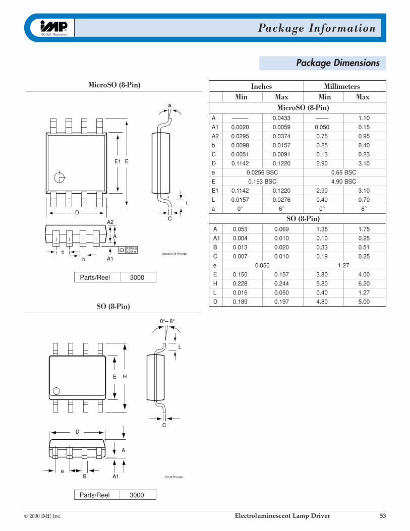
Package Information
© 2000 IMP, Inc. Electroluminescent Lamp Driver 53
L
0°– 8°
C
HE
e
D
B A1
A
SO (8-Pin).eps
Inches MillimetersMin Max Min Max
MicroSO (8-Pin)A ––––– 0.0433 –––– 1.10
A1 0.0020 0.0059 0.050 0.15
A2 0.0295 0.0374 0.75 0.95
b 0.0098 0.0157 0.25 0.40
C 0.0051 0.0091 0.13 0.23
D 0.1142 0.1220 2.90 3.10
e 0.0256 BSC 0.65 BSC
E 0.193 BSC 4.90 BSC
E1 0.1142 0.1220 2.90 3.10
L 0.0157 0.0276 0.40 0.70
a 0° 6° 0° 6°
SO (8-Pin)A 0.053 0.069 1.35 1.75
A1 0.004 0.010 0.10 0.25
B 0.013 0.020 0.33 0.51
C 0.007 0.010 0.19 0.25
e 0.050 1.27
E 0.150 0.157 3.80 4.00
H 0.228 0.244 5.80 6.20
L 0.016 0.050 0.40 1.27
D 0.189 0.197 4.80 5.00SO (8-Pin)
Package Dimensions
MicroSO (8-Pin)
e
b
D
E1 E
a
L
+
C
D 0.10mm0.004in
A1
A2
A
MicroSO (8-Pin).eps
Parts/Reel 3000
Parts/Reel 3000
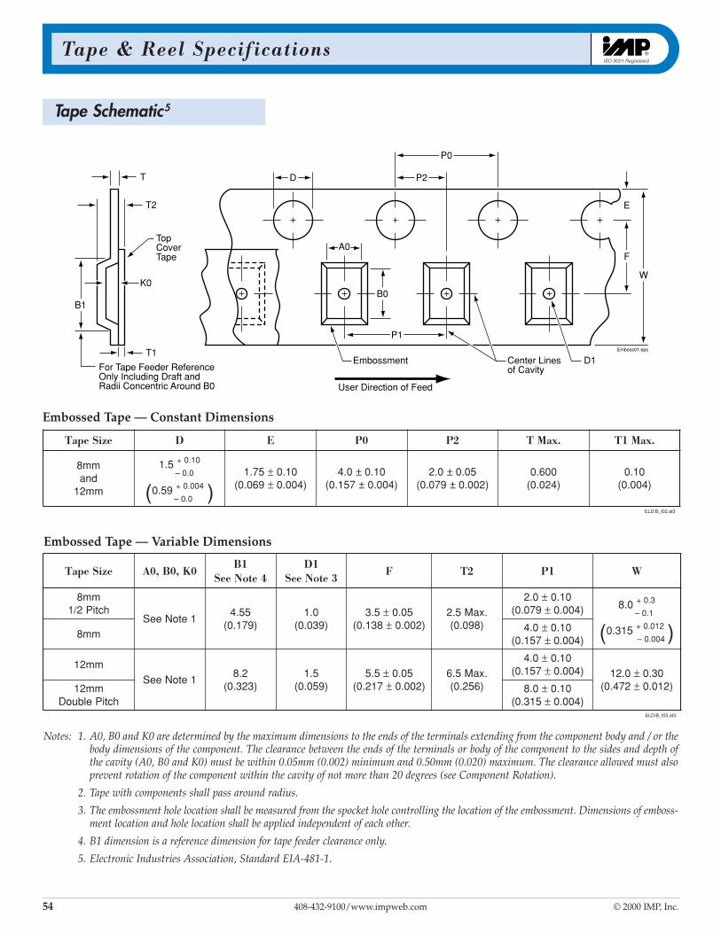
Tape & Reel Specif ications
54 408-432-9100/www.impweb.com © 2000 IMP, Inc. "
Tape Schematic5
Emboss01.eps
D P2
P0
A0
T
Embossment
User Direction of Feed
D1Center Linesof Cavity
P1
B0B1
F
E
W
T1
K0
T2
TopCoverTape
For Tape Feeder Reference Only Including Draft and Radii Concentric Around B0
eziSepaT D E 0P 2P .xaMT .xaM1T
mm8dnamm21
5.1 01.0+
0.0–
( 95.0 400.0+ )0.0–
57.1 ± 01.0960.0( ± )400.0
01.0±0.4)400.0±751.0(
50.0±0.2)200.0±970.0(
006.0)420.0(
01.0)400.0(
3ta.20t_B/DLE
eziSepaT 0K,0B,0A1B
4etoNeeS1D
3etoNeeSF 2T 1P W
mm8hctiP2/1
1etoNeeS55.4
)971.0(0.1
)930.0(5.3 ± 50.0831.0( ± )200.0
.xaM5.2)890.0(
0.2 ± 01.0970.0( ± )400.0 0.8 3.0+
1.0–
( 513.0 210.0+ )400.0–mm80.4 ± 01.0751.0( ± )400.0
mm211etoNeeS
2.8)323.0(
5.1)950.0(
5.5 ± 50.0712.0( ± )200.0
.xaM5.6)652.0(
0.4 ± 01.0751.0( ± )400.0 0.21 ± 03.0
274.0( ± )210.0mm21hctiPelbuoD
0.8 ± 01.0513.0( ± )400.0
3ta.30t_B/DLE
Notes: 1. A0, B0 and K0 are determined by the maximum dimensions to the ends of the terminals extending from the component body and / or thebody dimensions of the component. The clearance between the ends of the terminals or body of the component to the sides and depth ofthe cavity (A0, B0 and K0) must be within 0.05mm (0.002) minimum and 0.50mm (0.020) maximum. The clearance allowed must alsoprevent rotation of the component within the cavity of not more than 20 degrees (see Component Rotation).
2. Tape with components shall pass around radius.
3. The embossment hole location shall be measured from the spocket hole controlling the location of the embossment. Dimensions of emboss-ment location and hole location shall be applied independent of each other.
4. B1 dimension is a reference dimension for tape feeder clearance only.
5. Electronic Industries Association, Standard EIA-481-1.
Embossed Tape — Constant Dimensions
Embossed Tape — Variable Dimensions

Tape & Reel Specif ications
© 2000 IMP, Inc. Electroluminescent Lamp Driver 55
Tape Layout
Emboss04.eps
R Min.
Typical Component Center Line
Typical Component Cavity Center Line
20° Maximum Component Rotation
Emboss05.eps
1mm Max.
Allowable camber to be 1mm/100mm nonaccumulative over 250mm.
TAPE
1mm (.039) Max.
100mm (3.937)
250mm (9.843)
Emboss06.epsUser Direction of Feed
160mm (6.30) Min. Components390mm (15.35) Min.560mm (22.05) Max.
TopCoverTape
EndCarrier Tape
Cover Tape
Start
Component Rotation Bending Radius
Tape Camber (Top View)
Tape Leader and Trailer Dimensions
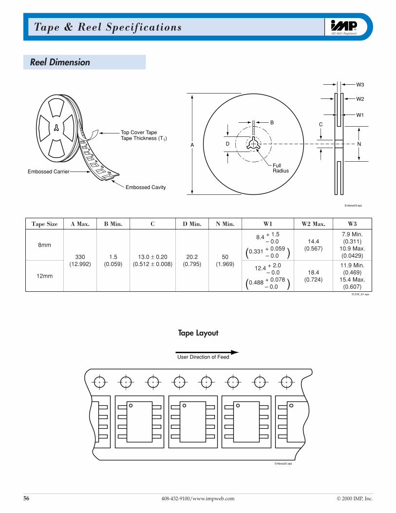
Tape & Reel Specif ications
56 408-432-9100/www.impweb.com © 2000 IMP, Inc. "
Reel Dimension
Emboss02.eps
User Direction of Feed
Emboss03.eps
B
W2
W1
W3
FullRadius
D
C
A
Embossed Carrier
Top Cover TapeTape Thickness (T1)
Embossed Cavity
N
eziSepaT .xaMA .niMB C .niMD .niMN 1W .xaM2W 3W
mm8
033)299.21(
5.1)950.0(
0.31 ± 02.0215.0( ± )800.0
2.02)597.0(
05)969.1(
4.8 5.1+0.0–
( 133.0 950.0+ )0.0–
4.41)765.0(
.niM9.7)113.0(
.xaM9.01)9240.0(
mm214.21 0.2+
0.0–
( 884.0 870.0+ )0.0–
4.81)427.0(
.niM9.11)964.0(
.xaM4.51)706.0(
spe.10t_B/DLE
Tape Layout

IMP Sales Off ices and Representatives
© 2000 IMP, Inc. Electroluminescent Lamp Driver 57
IMP, Inc.Corporate Headquarters2830 North First StreetSan Jose, CA 95134Main: 408.432.9100Sales: 408.434.1277Fax: 408.434.1215E-Mail: [email protected]: www.impweb.com
North American Sales Venkat VedireIMP, Inc.2830 North First StreetSan Jose, CA 95134Tel: 408.434.1427Fax: 408.434.5904E-Mail: [email protected]
Asia Pacific Area Sales OfficeHong Kong/China, Philippines Jacky KwokIMP, Inc.101 Kitchener Road, #02-08 Jalan Besar Plaza Singapore 208511 Phone: 65.296.0626 Fax: 65.398.0974E-Mail:[email protected]
Japan, Taiwan and Thailand Boon Chin PANG (FENG)IMP, Inc.101 Kitchener Road, #02-08 Jalan Besar Plaza Singapore 208511 Phone: 65.296.0626 Fax: 65.398.0974E-Mail: [email protected]
Singapore Mok Kwing YueIMP, Inc.101 Kitchener Road, #02-08 Jalan Besar Plaza Singapore 208511 Phone: 65.296.0626 Fax: 65.398.0974E-Mail:[email protected]
IMP Foundry ServicesMoiz KhambatyIMP, Inc.2830 North First StreetSan Jose, CA 95134Tel: 408.434.1206Fax: 408.434.1215E-Mail: [email protected]: www.impweb.com
North AmericanRepresentatives
AlabamaBITS, Inc.Huntsville, ALTel: 256.534.4020Fax: 256.534.0410URL: www.bits1.com
AlaskaELREPCO - NorthwestBeaverton, ORTel: 503.520.1900Fax: 503.520.1906
ArizonaNELCO Two CompanyChandler, AZTel: 408.726.2334Fax: 408 .726.2338
ArkansasIMP, Inc.San Jose, CATel: 408.434.1467Fax: 408.434.0335 E-Mail: [email protected]: www.impweb.com
California: NorthernQuorum Technical SalesSanta Clara, CATel: 408.980.0812Fax: 408.748.1163
Sacramento Reno AreaQuorum Technical SalesParadise, CATel: 530.877.5772Fax: 530.699.4007
California: SouthernSpectrum Rep CompanyWestlake VillageTel: 818.706.2919Fax: 818.706.2978
Rancho Santa Margarita, CATel: 949.766.6700Fax: 949.766.6701
Mission Viejo, CATel: 949.367.3132Fax: 949.367.3133
CanadaAstec Components Ltd.Mississauga, Ontario, CanadaTel: 905.607.1944Fax: 905.607.9991E-Mail: [email protected]: www.astec.ca
ColoradoPromoTech SalesWestminster, COTel: 303.920.2988Fax: 303.255.0701
ConnecticutAgile Electronic SalesNashua, NH 03062Tel: 603.595.8598Fax: 603.595.8579E-Mail: [email protected]
DelawareAstrorep Mid Atlantic, Inc.Warminister, PATel: 215.957.9580Fax: 215.957.9583URL: www.astrorep.com
FloridaMarathon Technical SalesOrlando, FLTel: 407.872.5775Tel: 800.713.9156Fax: 407.872.0535URL: www.marathontech.com
St. Petersburg, FLTel: 727.894.3603Fax: 727.894.3804URL: www.marathontech.com
Fort Lauderdale, FLTel: 954.527.4949Fax: 954.527.4115URL: www.marathontech.com
GeorgiaBITS, Inc.Lawrenceville, GATel: 770.513.8610Fax: 770.513.8680URL: www.bits1.com
IdahoNELCO Two CompanyBoise, IDTel: 208.343.9171Fax: 208.343.9170
IllinoisNorthern Illinois AreaHorizon Technical Sales, Inc.Downers Grove, ILTel: 630.852.2500Fax: 630.852.2520 Email:[email protected]:www.horizontechsales.com
Southern Illinois AreaCentral Tech Sales, Inc.St. Louis, MOTel: 314.878.6336Fax: 314.878.6550
IndianaSchillinger Associates, Inc.Kokomo, INTel: 765.457.7241Fax: 765.457.7732
IowaIMP, Inc.San Jose, CATel: 408.434.1467Fax: 408.434.0335Email: [email protected]: www.impweb.com
KansasCentral Tech Sales, Inc.St. Louis, MOTel: 314.878.6336Fax: 314.878.6550
KentuckySchillinger Associates, Inc.Kokomo, INTel: 765.457.7241Fax: 765.457.7732 URL: www.sai-rep.com
LouisianaIMP, Inc.San Jose, CATel: 408.434.1467Fax: 408.434.0335 E-Mail: [email protected]: www.impweb.com
MaineAgile Electronic Sales, LLC.Nashua, NH 03062Tel: 603.595.8598Fax: 603.595.8579E-Mail: [email protected]
MarylandAstrorep Mid Atlantic, Inc.Pasadena, MDTel: 410.255.8470Fax: 410.439.0339URL: www.astrorep.com
MassachusettsAgile Electronic Sales, LLC.Nashua, NH 03062Tel: 603.595.8598Fax: 603.595.8579E-Mail: [email protected]
MexicoIMP, Inc.San Jose, CATel: 408.434.1467Fax: 408.434.0335 E-Mail: [email protected]: www.impweb.com
MichiganSchillinger Associates, Inc.Kokomo, INTel: 765.457.7241Fax: 765.457.7732 URL: www.sai-rep.com
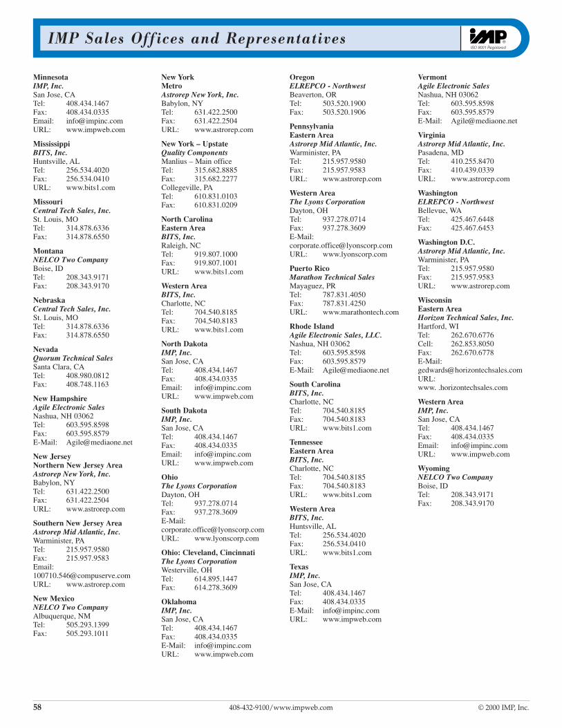
IMP Sales Off ices and Representatives
58 408-432-9100/www.impweb.com © 2000 IMP, Inc.
MinnesotaIMP, Inc.San Jose, CATel: 408.434.1467Fax: 408.434.0335Email: [email protected]: www.impweb.com
MississippiBITS, Inc.Huntsville, ALTel: 256.534.4020Fax: 256.534.0410URL: www.bits1.com
MissouriCentral Tech Sales, Inc.St. Louis, MOTel: 314.878.6336Fax: 314.878.6550
MontanaNELCO Two CompanyBoise, IDTel: 208.343.9171Fax: 208.343.9170
NebraskaCentral Tech Sales, Inc.St. Louis, MOTel: 314.878.6336Fax: 314.878.6550
NevadaQuorum Technical Sales Santa Clara, CATel: 408.980.0812 Fax: 408.748.1163
New HampshireAgile Electronic SalesNashua, NH 03062Tel: 603.595.8598Fax: 603.595.8579E-Mail: [email protected]
New JerseyNorthern New Jersey AreaAstrorep New York, Inc.Babylon, NYTel: 631.422.2500Fax: 631.422.2504URL: www.astrorep.com
Southern New Jersey AreaAstrorep Mid Atlantic, Inc.Warminister, PATel: 215.957.9580Fax: 215.957.9583Email:[email protected]: www.astrorep.com
New MexicoNELCO Two CompanyAlbuquerque, NMTel: 505.293.1399Fax: 505.293.1011
New YorkMetroAstrorep New York, Inc.Babylon, NYTel: 631.422.2500Fax: 631.422.2504URL: www.astrorep.com
New York – UpstateQuality ComponentsManlius – Main officeTel: 315.682.8885Fax: 315.682.2277Collegeville, PATel: 610.831.0103Fax: 610.831.0209
North CarolinaEastern AreaBITS, Inc.Raleigh, NCTel: 919.807.1000Fax: 919.807.1001URL: www.bits1.com
Western Area BITS, Inc.Charlotte, NCTel: 704.540.8185Fax: 704.540.8183URL: www.bits1.com
North DakotaIMP, Inc.San Jose, CATel: 408.434.1467Fax: 408.434.0335Email: [email protected]: www.impweb.com
South DakotaIMP, Inc.San Jose, CATel: 408.434.1467Fax: 408.434.0335Email: [email protected]: www.impweb.com
OhioThe Lyons CorporationDayton, OHTel: 937.278.0714Fax: 937.278.3609 E-Mail:[email protected] URL: www.lyonscorp.com
Ohio: Cleveland, CincinnatiThe Lyons CorporationWesterville, OHTel: 614.895.1447Fax: 614.278.3609
OklahomaIMP, Inc.San Jose, CATel: 408.434.1467Fax: 408.434.0335 E-Mail: [email protected]: www.impweb.com
OregonELREPCO - NorthwestBeaverton, ORTel: 503.520.1900Fax: 503.520.1906
PennsylvaniaEastern AreaAstrorep Mid Atlantic, Inc.Warminister, PATel: 215.957.9580Fax: 215.957.9583URL: www.astrorep.com
Western AreaThe Lyons CorporationDayton, OHTel: 937.278.0714Fax: 937.278.3609 E-Mail:[email protected] URL: www.lyonscorp.com
Puerto RicoMarathon Technical SalesMayaguez, PRTel: 787.831.4050Fax: 787.831.4250URL: www.marathontech.com
Rhode IslandAgile Electronic Sales, LLC.Nashua, NH 03062Tel: 603.595.8598Fax: 603.595.8579E-Mail: [email protected]
South CarolinaBITS, Inc.Charlotte, NCTel: 704.540.8185Fax: 704.540.8183URL: www.bits1.com
TennesseeEastern AreaBITS, Inc.Charlotte, NCTel: 704.540.8185Fax: 704.540.8183URL: www.bits1.com
Western AreaBITS, Inc.Huntsville, ALTel: 256.534.4020Fax: 256.534.0410URL: www.bits1.com
TexasIMP, Inc.San Jose, CATel: 408.434.1467Fax: 408.434.0335 E-Mail: [email protected]: www.impweb.com
VermontAgile Electronic SalesNashua, NH 03062Tel: 603.595.8598Fax: 603.595.8579E-Mail: [email protected]
VirginiaAstrorep Mid Atlantic, Inc.Pasadena, MDTel: 410.255.8470Fax: 410.439.0339URL: www.astrorep.com
WashingtonELREPCO - NorthwestBellevue, WATel: 425.467.6448Fax: 425.467.6453
Washington D.C.Astrorep Mid Atlantic, Inc.Warminister, PATel: 215.957.9580Fax: 215.957.9583URL: www.astrorep.com
WisconsinEastern AreaHorizon Technical Sales, Inc.Hartford, WITel: 262.670.6776Cell: 262.853.8050Fax: 262.670.6778 E-Mail:[email protected] URL:www. .horizontechsales.com
Western AreaIMP, Inc.San Jose, CATel: 408.434.1467Fax: 408.434.0335Email: [email protected]: www.impweb.com
WyomingNELCO Two CompanyBoise, IDTel: 208.343.9171Fax: 208.343.9170
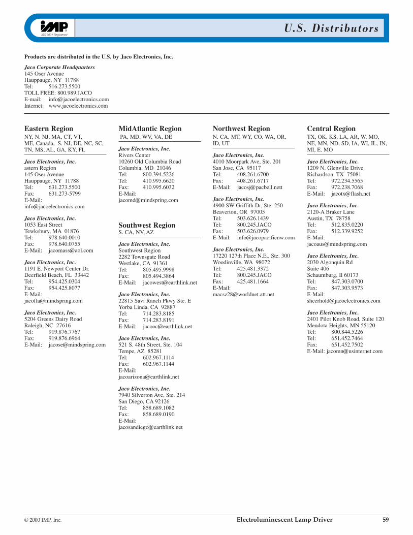
U.S. Distributors
© 2000 IMP, Inc. Electroluminescent Lamp Driver 59
Eastern RegionNY, N. NJ, MA, CT, VT, ME, Canada, S. NJ, DE, NC, SC,TN, MS, AL, GA, KY, FL
Jaco Electronics, Inc.astern Region145 Oser AvenueHauppauge, NY 11788Tel: 631.273.5500Fax: 631.273-5799 E-Mail:[email protected]
Jaco Electronics, Inc.1053 East StreetTewksbury, MA 01876Tel: 978.640.0010Fax: 978.640.0755E-Mail: [email protected]
Jaco Electronics, Inc.1191 E. Newport Center Dr.Deerfield Beach, FL 33442Tel: 954.425.0304Fax: 954.425.8077E-Mail:[email protected]
Jaco Electronics, Inc.5204 Greens Dairy RoadRaleigh, NC 27616Tel: 919.876.7767Fax: 919.876.6964E-Mail: [email protected]
MidAtlantic RegionPA, MD, WV, VA, DE
Jaco Electronics, Inc.Rivers Center10260 Old Columbia RoadColumbia, MD 21046 Tel: 800.394.5226Tel: 410.995.6620Fax: 410.995.6032E-Mail:[email protected]
Southwest RegionS. CA, NV, AZ
Jaco Electronics, Inc.Southwest Region2282 Townsgate RoadWestlake, CA 91361Tel: 805.495.9998Fax: 805.494.3864E-Mail: [email protected]
Jaco Electronics, Inc.22815 Savi Ranch Pkwy Ste. EYorba Linda, CA 92887Tel: 714.283.8185Fax: 714.283.8191E-Mail: [email protected]
Jaco Electronics, Inc.521 S. 48th Street, Ste. 104Tempe, AZ 85281Tel: 602.967.1114Fax: 602.967.1144E-Mail:[email protected]
Jaco Electronics, Inc.7940 Silverton Ave, Ste. 214San Diego, CA 92126 Tel: 858.689.1082Fax: 858.689.0190E-Mail:[email protected]
Northwest RegionN. CA, MT, WY, CO, WA, OR,ID, UT
Jaco Electronics, Inc.4010 Moorpark Ave, Ste. 201San Jose, CA 95117Tel: 408.261.6700Fax: 408.261.6717E-Mail: [email protected]
Jaco Electronics, Inc.4900 SW Griffith Dr, Ste. 250Beaverton, OR 97005Tel: 503.626.1439Tel: 800.245.JACOFax: 503.626.0979E-Mail: [email protected]
Jaco Electronics, Inc.17220 127th Place N.E., Ste. 300Woodinville, WA 98072Tel: 425.481.3372Tel: 800.245.JACOFax: 425.481.1664E-Mail:[email protected]
Central RegionTX, OK, KS, LA, AR, W. MO,NE, MN, ND, SD, IA, WI, IL, IN,MI, E. MO
Jaco Electronics, Inc.1209 N. Glenville DriveRichardson, TX 75081Tel: 972.234.5565Fax: 972.238.7068E-Mail: [email protected]
Jaco Electronics, Inc.2120-A Braker LaneAustin, TX 78758Tel: 512.835.0220Fax: 512.339.9252E-Mail:[email protected]
Jaco Electronics, Inc.2030 Algonquin RdSuite 406Schaumburg, Il 60173 Tel: 847.303.0700Fax: 847.303.9573E-Mail:[email protected]
Jaco Electronics, Inc.2401 Pilot Knob Road, Suite 120Mendota Heights, MN 55120 Tel: 800.844.5226Tel: 651.452.7464Fax: 651.452.7502E-Mail: [email protected]
Products are distributed in the U.S. by Jaco Electronics, Inc.
Jaco Corporate Headquarters145 Oser AvenueHauppauge, NY 11788Tel: 516.273.5500TOLL FREE: 800.989.JACOE-mail: [email protected]: www.jacoelectronics.com
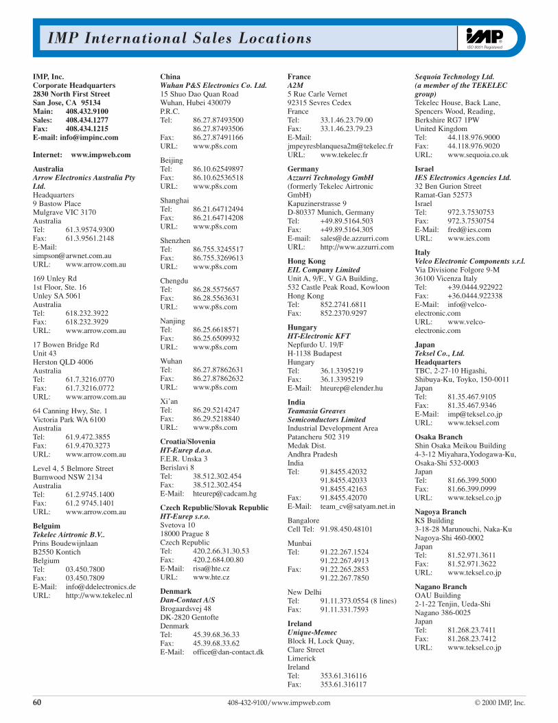
IMP International Sales Locations
60 408-432-9100/www.impweb.com © 2000 IMP, Inc.
IMP, Inc.Corporate Headquarters2830 North First StreetSan Jose, CA 95134Main: 408.432.9100Sales: 408.434.1277Fax: 408.434.1215E-mail: [email protected]
Internet: www.impweb.com
AustraliaArrow Electronics Australia PtyLtd.Headquarters9 Bastow PlaceMulgrave VIC 3170AustraliaTel: 61.3.9574.9300Fax: 61.3.9561.2148E-Mail:[email protected]: www.arrow.com.au
169 Unley Rd1st Floor, Ste. 16Unley SA 5061AustraliaTel: 618.232.3922Fax: 618.232.3929URL: www.arrow.com.au
17 Bowen Bridge RdUnit 43Herston QLD 4006AustraliaTel: 61.7.3216.0770Fax: 61.7.3216.0772URL: www.arrow.com.au
64 Canning Hwy, Ste. 1Victoria Park WA 6100AustraliaTel: 61.9.472.3855Fax: 61.9.470.3273URL: www.arrow.com.au
Level 4, 5 Belmore StreetBurnwood NSW 2134AustraliaTel: 61.2.9745.1400Fax: 61.2 9745.1401URL: www.arrow.com.au
BelguimTekelec Airtronic B.V..Prins BoudewijnlaanB2550 KontichBelgiumTel: 03.450.7800Fax: 03.450.7809E-Mail: [email protected]: http://www.tekelec.nl
ChinaWuhan P&S Electronics Co. Ltd.15 Shuo Dao Quan RoadWuhan, Hubei 430079P.R.C.Tel: 86.27.87493500
86.27.87493506Fax: 86.27.87491166URL: www.p8s.com
BeijingTel: 86.10.62549897Fax: 86.10.62536518URL: www.p8s.com
ShanghaiTel: 86.21.64712494Fax: 86.21.64714208URL: www.p8s.com
ShenzhenTel: 86.755.3245517Fax: 86.755.3269613URL: www.p8s.com
ChengduTel: 86.28.5575657Fax: 86.28.5563631URL: www.p8s.com
NanjingTel: 86.25.6618571Fax: 86.25.6509932URL: www.p8s.com
WuhanTel: 86.27.87862631Fax: 86.27.87862632URL: www.p8s.com
Xi’anTel: 86.29.5214247Fax: 86.29.5218840URL: www.p8s.com
Croatia/SloveniaHT-Eurep d.o.o.F.E.R. Unska 3Berislavi 8Tel: 38.512.302.454Fax: 38.512.302.454E-Mail: [email protected]
Czech Republic/Slovak RepublicHT-Eurep s.r.o.Svetova 1018000 Prague 8Czech RepublicTel: 420.2.66.31.30.53Fax: 420.2.684.00.80E-Mail: [email protected]: www.hte.cz
DenmarkDan-Contact A/SBrogaardsvej 48DK-2820 GentofteDenmarkTel: 45.39.68.36.33Fax: 45.39.68.33.62E-Mail: [email protected]
FranceA2M5 Rue Carle Vernet92315 Sevres CedexFranceTel: 33.1.46.23.79.00Fax: 33.1.46.23.79.23E-Mail:[email protected] URL: www.tekelec.fr
GermanyAzzurri Technology GmbH(formerly Tekelec AirtronicGmbH)Kapuzinerstrasse 9D-80337 Munich, GermanyTel: +49.89.5164.503Fax: +49.89.5164.305E-mail: [email protected]: http://www.azzurri.com
Hong KongEIL Company LimitedUnit A, 9/F., V GA Building,532 Castle Peak Road, KowloonHong KongTel: 852.2741.6811Fax: 852.2370.9297
HungaryHT-Electronic KFTNepfurdo U. 19/FH-1138 BudapestHungaryTel: 36.1.3395219Fax: 36.1.3395219E-Mail: [email protected]
IndiaTeamasia GreavesSemiconductors LimitedIndustrial Development AreaPatancheru 502 319Medak Dist.Andhra PradeshIndiaTel: 91.8455.42032
91.8455.4203391.8455.42163
Fax: 91.8455.42070 E-Mail: [email protected]
BangaloreCell Tel: 91.98.450.48101
Munbai Tel: 91.22.267.1524
91.22.267.4913Fax: 91.22.265.2853
91.22.267.7850
New DelhiTel: 91.11.373.0554 (8 lines)Fax: 91.11.331.7593
IrelandUnique-MemecBlock H, Lock Quay,Clare StreetLimerickIrelandTel: 353.61.316116Fax: 353.61.316117
Sequoia Technology Ltd. (a member of the TEKELEC group)Tekelec House, Back Lane,Spencers Wood, Reading,Berkshire RG7 1PWUnited KingdomTel: 44.118.976.9000Fax: 44.118.976.9020URL: www.sequoia.co.uk
IsraelIES Electronics Agencies Ltd.32 Ben Gurion StreetRamat-Gan 52573IsraelTel: 972.3.7530753Fax: 972.3.7530754 E-Mail: [email protected]: www.ies.com
ItalyVelco Electronic Components s.r.l.Via Divisione Folgore 9-M36100 Vicenza ItalyTel: +39.0444.922922Fax: +36.0444.922338E-Mail: [email protected]: www.velco-electronic.com
JapanTeksel Co., Ltd.HeadquartersTBC, 2-27-10 Higashi,Shibuya-Ku, Toyko, 150-0011JapanTel: 81.35.467.9105Fax: 81.35.467.9346E-Mail: [email protected]: www.teksel.com
Osaka BranchShin Osaka Meikou Building4-3-12 Miyahara,Yodogawa-Ku,Osaka-Shi 532-0003 JapanTel: 81.66.399.5000Fax: 81.66.399.0999URL: www.teksel.co.jp
Nagoya BranchKS Building3-18-28 Marunouchi, Naka-KuNagoya-Shi 460-0002 JapanTel: 81.52.971.3611Fax: 81.52.971.3622URL: www.teksel.co.jp
Nagano BranchOAU Building2-1-22 Tenjin, Ueda-ShiNagano 386-0025 JapanTel: 81.268.23.7411Fax: 81.268.23.7412URL: www.teksel.co.jp
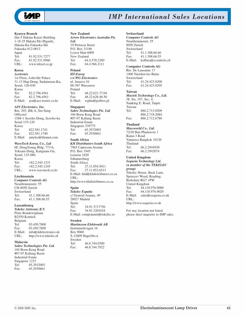
IMP International Sales Locations
© 2000 IMP, Inc. Electroluminescent Lamp Driver 61
Kyusyu BranchDai-5 Hakata Kaisei Building1-18-25 Hakata Eki-Higashi,Hakata-Ku Fukuoka-ShiFukuoka 812-0013JapanTel: 81.92.531.7277Fax: 81.92.531.9960URL: www.teksel.co.jp
KoreaAcetronix1st Floor, Ashiville Palace31-13 Hap-Dong, Sudaimoon-Ku,Seoul, 120-030KoreaTel: 82.2.796.4561Fax: 82.2.796.4563E-Mail: [email protected]
AIN Electronics, Inc.Rm. 203, Blk A, Sin-SungOfficetel1588-1 Seocho-Dong, Seocho-kuSeoul 135-120KoreaTel: 822.581.1741Fax: 822.581.1740 E-Mail: [email protected]
WaveTech Korea, Co., Ltd6F, DongYoung Bldg, 773-6,Yoksam-Dong, Kangnam-Gu,Seoul, 135-080.KoreaTel: +82.2.545.1231Fax: +82.2.545.1245URL: www.wavetech.co.kr
LiechtensteinComputer Controls AGNeunbrunnenstr. 55CH-8050 ZurichSwitzerlandTel: 41.1.308.66.66Fax: 41.1.308.66.55
LuxembourgTekelec Airtronic B.V.Prins BoudewijnlaanB2550 KontichBelgiumTel: 03.450.7800Fax: 03.450.7809E-Mail: [email protected]: http://www.tekelec.nl
MalaysiaSabre Technologies Pte. Ltd.104 Boon Keng Road#07-07 Kallang BasinIndustrial EstateSingapore 1233Tel: 65.2932003Fax: 65.2930661
New ZealandArrow Electronics Australia PtyLtd.19 Pretocia StreetP.O. Box 31186Lower Hutt 6009New ZealandTel: 64.4.570.2260Fax: 64.4.566.2111
PolandHT-Eurepc/o WG Electronicsul. Jarazca 1000-387 WarszawaPolandTel: 48.22.621.77.04Fax: 48.22.628.48.50E-Mail: [email protected]
SingaporeSabre Technologies Pte. Ltd.104 Boon Keng Road#07-07 Kallang BasinIndustrial EstateSingapore 339775Tel: 65.2932003Fax: 65.2930661
South AfricaKH Distributors-South Africa7965 Capricorn AvenueP.O. Box 1945Lenasia 1820JohannesburgSouth AfricaTel: 27.11.854.5011Fax: 27.11.852.6513E-Mail: [email protected]:http://www.khdistributors.co.za
SpainTekelec Españac/ General Aranaz, 4928027 MadridSpainTel: 34.91.3717756Fax: 34.91.3201018E-Mail: [email protected]
SwedenMartinsson Elektronik ABInstrumentvagen 16Box 9060S-12609 HagerSte.nSwedenTel: 46.8.744.0300Fax: 46.8.744.7922
SwitzerlandComputer Controls AGNeunbrunnenstr. 558050 ZurichSwitzerlandTel: 41.1.308.66.66Fax: 41.1.308.66.55E-Mail: [email protected]
Computer Controls AGRte. De Lausanne 171400 Yuerdon-les-BainsSwitzerlandTel: 41.24.423.8200Fax: 41.24.423.8205
TaiwanMaxtek Technology Co., Ltd.3F, No. 197, Sec. 4, Nanking E. Road, TaipeiTaiwanTel: 886.2.713.0209
886.2.718.2084Fax: 886.2.712.6780
ThailandMassworld Co., Ltd.72/30 Ban Phunravee 1Rama 3 RoadYannawa Bangkok 10120ThailandTel: 66.2.2944930Fax: 66.2.2942074
United KingdomSequoia Technology Ltd. (a member of the TEKELEC group)Tekelec House, Back Lane,Spencers Wood, Reading,Berkshire RG7 1PWUnited KingdomTel: 44.118.976.9000Fax: 44.118.976.9020E-Mail: [email protected] URL:http://www.sequoia.co.uk
For any location not listed,please diect inquiries to IMP sales.

Map to IMP - San Jose, CA, USA
62 408-432-9100/www.impweb.com © 2000 IMP, Inc. "
For Additional Directions408-432-9100
Trim
bleRd
Colem
an
Ave
nue
LafayetteS
treet
Brokaw Road
Tasman Drive
Charcot
Montague Exwy
Airport Blvd
880
101
237
Zanker
Road
San JoseInternational
Airport
Terminal ALegion
Terminal C
To San FranciscoInternational
Airport
To OaklandInternational
Airport
70 Daggett DriveBuilding 2San Jose, CA 95134-2108
2830 N. First StreetBuilding 1San Jose, CA 95134-2071
North First Street
CentralExpressway
GuadalupePkw
y
Zanker Rd
North
First Street
D rive
Junction Ave
East
Plum
eria
Dag
gett
Airpor
t Pkw
y
Montague Exwy
From Oakland International AirportGo South on 880 and turn right at the Montague Expresswayexit, move left out of the car pool lane. Turn left on ZankerRoad and then turn right on Daggett Drive.
From San Francisco International AirportGo South on 101 to the Montague Expressway exit(east). Turn right on Zanker Road and then turn righton Daggett Drive.
From San Jose International AirportFrom Terminal Drive go to Airport Blvd. From AirportBlvd., turn onto Airport Pkwy. (Airport Pkwy becomesBrokaw Road after 101). Turn left on North First Street,then turn right on Daggett Drive.

Quality at IMP - Our Policy
© 2000 IMP, Inc. Electroluminescent Lamp Driver 63
Quality PriorityQuality in everything we do is a fundamental IMP commitment. Quality may not be sacrificed for any other priority. Before any action is taken, the effect on quality as seen byemployees and by customers must be considered.
Product Quality ConformanceProducts and services for our customers will conform to all requirements. Products will meet performance specifications. Services will be complete, meet described requirements, and will be in a format appropriate for the customer’s use. If a specification cannot be met in full, the customer will be advised and a new specification will be negotiated.
Product and Process Quality ImprovementAll processes, manufacturing, manufacturing planning, customer service, product design anddesign of manufacturing processes shall utilize Total Quality Management concepts including Statistical Process Control techniques and designed experiments to ensure continualimprovement of products and services.
Employee ResponsibilityEach employee is responsible for performing their work correctly and completely. This responsibil-ity for quality performance applies to all design work, development work, manufacturing work andto all supporting work. It applies to all employee levels. It cannot be abandoned or delegated. Noone else can take responsibility.
IMP’s Commitment of SupportIMP will provide the tools, the training, and the time necessary for employees to meet theirresponsibilities.
Employee ParticipationIMP encourages all employees to take part in the open discussion, analysis and resolution of problems through participation in quality and productivity teams or through personal suggestions.
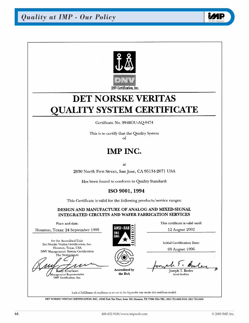
Quality at IMP - Our Policy
64 408-432-9100/www.impweb.com © 2000 IMP, Inc. "

Power Management Products
© 2000 IMP, Inc. Electroluminescent Lamp Driver 65
IMP offers higher performance, lower-power microprocessor supervisors that are pin compatible with devices from DallasSemiconductor and Maxim Integrated Products. For the latest information visit www.impweb.com or send specific requests [email protected].
µP Supervisor Products: Low Power Alternatives to MaximtraP
rebmuNdlohserhT)V(egatloV
yrettaBpukcaBhctiwS
godhctaWremiT
liaFrewoProtinoM
launaMteseR
TESERytiraloP
A096PMI 56.4 # # # WOL
A296PMI 04.4 # # # WOL
507PMI 56.4 # # # WOL
607PMI 04.4 # # # WOL
707PMI 56.4 # # H&L
807PMI 04.4 # # H&L
L208PMI 56.4 # # # WOL
M208PMI 04.4 # # # WOL
L508PMI 56.4 # # # HGIH
908PMI 36.4ot36.2 WOL
018PMI 36.4ot36.2 HGIH
118PMI 36.4ot36.2 # WOL
218PMI 36.4ot36.2 # HGIH
L318PMI 56.4 # # # HGIH60t_B/DLE
+
+
+ +
+
+
+
+
VCC
VOUT
1
7
5
3
PFI
WDI
GND
VBATT8
2
6
4 PFO
RESET(RESET)
( ) IMP805L
Battery-SwitchoverCircuit
ResetGenerator
WatchdogTimer3.5V
1.25V
1.25V0.8V
690A_03x.eps
1.25V –
+
MR
WDI WDO
RESET(RESET)(IMP813L)
PFO
GND
VCC
0.25mA
RESETGenerator
4.65V (IMP705/813L)4.40V (IMP706)
VCC
+ –
+
PFI
Timebase
WatchdogTimer
TransitionDetector
705_01x.eps
RESET
RESET
VCC
0.25mA
RESETGenerator
4.65V (IMP707)4.40V (IMP708)
VCC
+ –
+
MR
PFO
GND
1.25V –
+PFI
705_02x.eps
Block Diagrams
IMP690A, IMP692A, IMP802L,IMP802M and IMP805L IMP705, IMP706 and IMP813L IMP707 and IMP708

Power Management Products
66 408-432-9100/www.impweb.com © 2000 IMP, Inc. "
µP Supervisor Products: Low Power Alternatives to Dallas Semiconductor*gniredrOPMI
rebmuNtraPTESER
)V(egatloVTESER
)%(ecnareloTTESER
)sm(emiTTESERytiraloP
lluP-hsuPegatStuptuO
niarDnepOtuptuO
OSniP-8egakcaP
32-TOSegakcaP
322-TOSegakcaP
T/5-R0181PMI 026.4 5 051 WOL # #
T/01-R0181PMI 073.4 01 051 WOL # #
T/51-R0181PMI 021.4 51 051 WOL # #
T/5-R1181PMI 026.4 5 051 WOL # #
T/01-R1181PMI 053.4 01 051 WOL # #
T/51-R1181PMI 031.4 51 051 WOL # #
T/5-R2181PMI 026.4 5 051 HGIH # #
T/01-R2181PMI 053.4 01 051 HGIH # #
T/51-R2181PMI 031.4 51 051 HGIH # #
T/5-R5181PMI 060.3 5 051 WOL # #
T/01-R5181PMI 088.2 01 051 WOL # #
T/02-R5181PMI 055.2 02 051 WOL # #
T/5-R6181PMI 060.3 5 051 WOL # #
T/01-R6181PMI 088.2 01 051 WOL # #
T/02-R6181PMI 055.2 02 051 WOL # #
T/5-R7181PMI 060.3 5 051 HGIH # #
T/01-R7181PMI 088.2 01 051 HGIH # #
T/02-R7181PMI 055.2 02 051 HGIH # #
T/5-ZD3321PMI 526.4 5 053 WOL # #
T/01-ZD3321PMI 573.4 01 053 WOL # #
T/51-ZD3321PMI 521.4 51 053 WOL # #
T/55-SM3321PMI 526.4 5 053 WOL # #
T/5-SM3321PMI 573.4 01 053 WOL # #
T/3-SM3321PMI 027.2 51 053 WOL # #
.leeRdnaepaTsetacidniT/* 70t_B/DLE

Power Management Products
© 2000 IMP, Inc. Electroluminescent Lamp Driver 67
USB Power Switches
rebmuNtraP sehctiwSforebmuNdaoL-nepO
noitcnuFnoitceteD"NO"mumixaM
m(ecnatsiseR Ω) ytiraloPelbanE5052PMI 1 SEY 05 HGIH
1-5052PMI 1 ON 05 HGIH
2-5052PMI 1 ON 05 WOL
3-5052PMI 1 SEY 05 WOL
1-4252PMI 4 ON 041 HGIH
2-4252PMI 4 ON 041 WOL
1-5252PMI 1 ON 041 HGIH
2-5252PMI 1 ON 041 WOL
1-A5252PMIecnatsiseRNOwoL 1 ON 07 HGIH
2-A5252PMIecnatsiseRNOwoL 1 ON 07 WOL
1-6252PMI 2 ON 041 HGIH
2-6252PMI 2 ON 041 WOL
1-7252PMI 4 ON 003 HGIH
2-7252PMI 4 ON 003 WOL80t_B/DLE
IMP offers a full complement of Universal Serial Bus (USB)power switches that are higher-performance equivalents todevices from Micrel.
68 408-432-9100/www.impweb.com © 2000 IMP, Inc. "
Name:
Position:
Company:
Address:
City: State/Province:
Zip Code: Country:
Phone #: Fax #:
Email Address:
IMP Part Qty
IMP522EMB IMP525EMA IMP525ESAIMP527EMAIMP527ESA
ISO 9001 Registered®
www.impweb.comPhone: 408.432.9100 BRC02.eps-07/18/00
Sample Requests and New Product Updates
IMP Part Qty
IMP528EMAIMP528ESAIMP560EMAIMP560ESAIMP803LGIMP803IMA
Fax to408.434.0335

IMP, Inc.Corporate Headquarters2830 N. First StreetSan Jose, CA 95134-2071Tel: 408-432-9100Fax: 408-434-5904e-mail: [email protected]://www.impweb.com
The IMP logo is a registered trademark of IMP, Inc.
All other company and product names are trademarks of their respective owners.
April 2001© 2001 IMP, Inc.Printed in USAPublication #: 2008Revision: HIssue Date: 04/13/2001Type: Production


