17th World Conference on Nondestructive Testing, 25-28 Oct 2008, Shanghai, China Electromagnetic imaging using probe arrays Gerhard MOOK, Fritz MICHEL, Jouri SIMONIN Institute of Materials and Joining Technology, Otto-von-Guericke-University of Magdeburg, Magdeburg, Germany, Phone: +49 391 6714555, Fax: +49 391 6714569, e-mail: [email protected]; [email protected]; [email protected]Abstract Electromagnetic methods like eddy current technique do not provide images but only produce local signals in a difficult to understand measurement plane. Filters, thresholds and phase rotators are common tools of signal processing unable to bring up all information contained in the signals. Trials to generate images comparable to x-rays mostly base on costly and time consuming mechanical surface scanning. The paper presents theoretical and experimental steps ahead to modular 1D, 2D and 3D probe arrays for eddy current inspection. In contrary to other attempts these arrays work at low frequencies able to penetrate below the surface and provide good lateral resolution. That way they bring up not only surface but also hidden defects and anomalies. Potential applications are outlined. Keywords: Electromagnetic inspection, eddy current inspection, line sensor, sensor arrays 1 Electromagnetic imaging An open coil system fed by an alternating current induces eddy currents in a conductive material. The density and spatial distribution of these currents depends on the coil geometry, the frequency and some material properties like conductivity, magnetic permeability and geometry. The eddy currents build up a responding electromagnetic field interfering with the exciting field. Depending on the resultant field the coil system provides complex valued signals carrying information about the material properties. To generate a fingerprint of the electromagnetic properties of the material a single probe (coil system) scans the surface track by track. The real and the imaginary part of the probe signal are processed according to the material properties of interest [1-3]. The resultant complex signal is displayed correspondingly to the probe position. Within one scan of the probe two pictures may be recorded; one representing the real part and the other representing the imaginary part of the signal. Figure 1 illustrates this method.
Transcript
17th World Conference on Nondestructive Testing, 25-28 Oct 2008, Shanghai, China
Electromagnetic imaging using probe arrays
Gerhard MOOK, Fritz MICHEL, Jouri SIMONIN
Institute of Materials and Joining Technology, Otto-von-Guericke-University of Magdeburg,
Electromagnetic methods like eddy current technique do not provide images but only produce local signals in a difficult to understand measurement plane. Filters, thresholds and phase rotators are common tools of signal processing unable to bring up all information contained in the signals. Trials to generate images comparable to x-rays mostly base on costly and time consuming mechanical surface scanning.
The paper presents theoretical and experimental steps ahead to modular 1D, 2D and 3D probe arrays for eddy current inspection. In contrary to other attempts these arrays work at low frequencies able to penetrate below the surface and provide good lateral resolution. That way they bring up not only surface but also hidden defects and anomalies. Potential applications are outlined.
Keywords: Electromagnetic inspection, eddy current inspection, line sensor, sensor arrays
1 Electromagnetic imaging
An open coil system fed by an alternating current induces eddy currents in a conductive
material. The density and spatial distribution of these currents depends on the coil geometry, the
frequency and some material properties like conductivity, magnetic permeability and geometry.
The eddy currents build up a responding electromagnetic field interfering with the exciting field.
Depending on the resultant field the coil system provides complex valued signals carrying
information about the material properties.
To generate a fingerprint of the electromagnetic properties of the material a single probe (coil
system) scans the surface track by track. The real and the imaginary part of the probe signal are
processed according to the material properties of interest [1-3]. The resultant complex signal is
displayed correspondingly to the probe position. Within one scan of the probe two pictures may
be recorded; one representing the real part and the other representing the imaginary part of the
signal. Figure 1 illustrates this method.
The advantage of this single probe scanning is a high quality of imaging due to the constant
probe characteristics [4, 5]. The drawbacks are the expensive scanners and the time consuming
imaging process. Additionally, scanners are limited to simply shaped objects like flat or uniaxial
bent surfaces. More complicated surfaces have to be inspected manually without imaging.
Figure 1. Electromagnetic imaging using a single scanning eddy current probe.
2 Sensor elements
Eddy current method is most suited for inspecting the surface and near surface regions. The
penetration depth is limited by the skin effect and depends on the material properties and the
inspection frequency. The lower the frequency the deeper the eddy currents penetrate into the
material. But the lower the frequency the lower is also the sensitivity of the receiver coil. To
increase the low frequency performance of receiver coil one can use more windings, high
permeable ferrite cores or sophisticated balancing of two or more coils. On the other hand,
attempts have been made to substitute inductive receivers by new magneto-resistors [6-8]. These
elements are able to sense even DC fields. Their drawbacks are non-linearity, saturation,
hysteresis effects and the demand for DC offset. Until now, newly developed inductive receivers
perform not worse the magneto-resistors and are easier to handle.
One kind of inductive probes with increased inspection depth is the non-axial transmit-
receive probe sometimes called half transmission or even remote field probe [9]. These probes
offer the opportunity to optimize the distance between the transmitting and the receiving coil.
Figure 2 brings up the principle of those probes. The magnetic field of the exciting coil
penetrates accordingly to the well known rules of alternating field spreading into the material.
The receiving coil only picks up this part of the flux, which has penetrated deeply into the
material. The larger the spacing between the two coils the deeper the detected flux lines have
penetrated into the material but the lower becomes the measurement signal.
This system of two non-axial coils may be considered as an axial coil system with a diameter
corresponding to the coil distance of the non-axial system. With increasing distance (or diameter)
of the coils the defect volume decreases relatively to the volume of interaction lowering the
signal amplitude. One has to trade off between these parameters.
Figure 2. Non-axial probe selects deep penetration field trajectories.
Figure 3 displays the Point Spread Function of this probe. It differs significantly from that of
common axial eddy current probes [2] and is most suitable for imaging applications.
Figure 3. Calculated signal distribution of a small hidden pore, z - signal magnitude (arb. units), x and y - position of the pore.
For assessing the chances for defect characterization the complex values of the measurement
voltage were calculated for different inspection situations. Commonly all defect signals are
referred to the lift-off signal. For calculating the VIC-3D code was used.
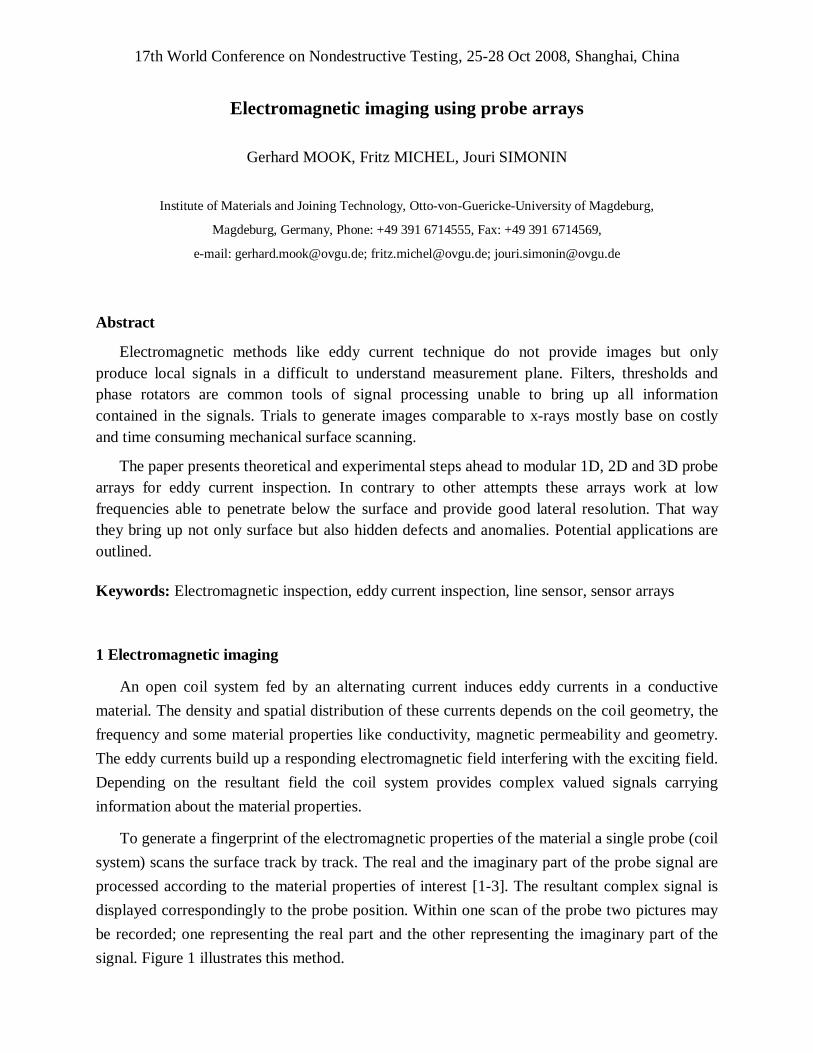
Figure 4 brings up the signal behaviour of a pore with defined underlying [10, 11]. Over the
sound material the signal is centred at the balance point. When approximating a defect the signal
trajectory starts with negative y-values. Just like axial probes the signal turns to positive y-values
over the defect. The defect signal turns clockwise with increasing defect underlying. This
circumstance opens up the opportunity of assessing the defect underlying. The signal magnitude
mirrors the defect volume.
Figure 4. Complex measurement signal of a non-axial probe moving over hidden pores of 2 mm diameter.
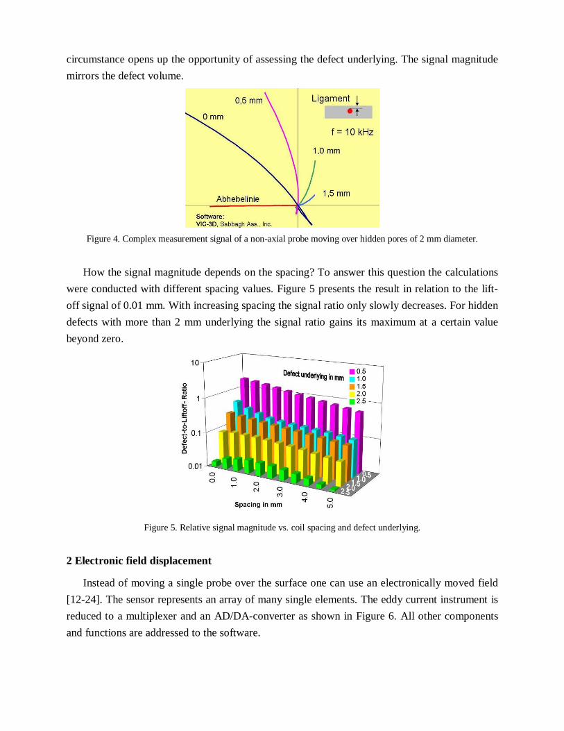
How the signal magnitude depends on the spacing? To answer this question the calculations
were conducted with different spacing values. Figure 5 presents the result in relation to the lift-
off signal of 0.01 mm. With increasing spacing the signal ratio only slowly decreases. For hidden
defects with more than 2 mm underlying the signal ratio gains its maximum at a certain value
beyond zero.
Figure 5. Relative signal magnitude vs. coil spacing and defect underlying.
2 Electronic field displacement
Instead of moving a single probe over the surface one can use an electronically moved field
[12-24]. The sensor represents an array of many single elements. The eddy current instrument is
reduced to a multiplexer and an AD/DA-converter as shown in Figure 6. All other components
and functions are addressed to the software.
Figure 6. Hardware components of the all-digital eddy current instrument with moving field sensor.
2.1 Sensor line
In a first attempt 32 sensor elements were combined in a multiplexed sensor line. The speed
of electronic field movement ranges from 0.4 to 3 m/s according to the inspection requirements.
To visualize a certain area of the workpiece the sensor line must be guided over the surface.
When handled manually a wheel connected to the sensor picks up the distance. In automatic
inspection a robot can guide the sensor with constant velocity from 6 to 48 mm/s. Figure 7
presents a result of hidden holes in an aluminium plate and figure 8 displays a real aluminium
cast with hidden anomalies. Potential applications also cover curved surfaces like pipes, rods or
rails.
Figure 7. Visualization of hidden defects in aluminium, left: moving field sensor,
right: y-component image of the plate.
Figure 8. Visualization of hidden anomalies in aluminium cast: a) Photograph of the area of interest, b) electromagnetic signature of this area, c) Photograph after 1 mm rework brings up the anomaly visually.
2.1 Flat array
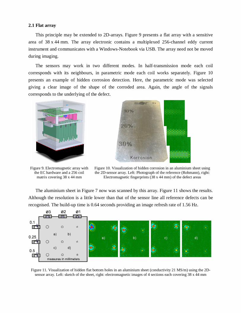
This principle may be extended to 2D-arrays. Figure 9 presents a flat array with a sensitive
area of 38 x 44 mm. The array electronic contains a multiplexed 256-channel eddy current
instrument and communicates with a Windows-Notebook via USB. The array need not be moved
during imaging.
The sensors may work in two different modes. In half-transmission mode each coil
corresponds with its neighbours, in parametric mode each coil works separately. Figure 10
presents an example of hidden corrosion detection. Here, the parametric mode was selected
giving a clear image of the shape of the corroded area. Again, the angle of the signals
corresponds to the underlying of the defect.
Figure 9. Electromagnetic array with
the EC hardware and a 256 coil matrix covering 38 x 44 mm
Figure 10. Visualization of hidden corrosion in an aluminium sheet using the 2D-sensor array. Left: Photograph of the reference (Rohmann), right:
Electromagnetic fingerprints (38 x 44 mm) of the defect areas
The aluminium sheet in Figure 7 now was scanned by this array. Figure 11 shows the results.
Although the resolution is a little lower than that of the sensor line all reference defects can be
recognised. The build-up time is 0.64 seconds providing an image refresh rate of 1.56 Hz.
Figure 11. Visualization of hidden flat bottom holes in an aluminium sheet (conductivity 21 MS/m) using the 2D-
sensor array. Left: sketch of the sheet, right: electromagnetic images of 4 sections each covering 38 x 44 mm
For increasing the signal-to-noise-ratio the software can integrate over a selectable number of
subsequent images. The images may be stored for quality documentation or defect growth
analysis. Basing on the magnitude and the angle of the defect signal in the complex measurement
plane defect classification becomes possible.
2.2 Free-form array
Although not flexible the coil arrangement may adapt to the inspection surface by moulding
techniques. Once moulded and cured the array forms a solid body easy to handle. As an example
a spherical surface was transferred to the array. Figure 12 gives an idea of the array and the
aluminium reference.
Figure 12. Visualization of hidden holes in an aluminium hemisphere using a free-form sensor array. Left top: Sketch of the array, left bottom: sketch of the reference, right: electromagnetic fingerprints of the defect area
Conclusion
The moving electromagnetic field sensor has the potential to visualize and to quantify hidden defects. The handling becomes much easier reducing the cost of the scanning system significantly. The hardware costs are reduced to a minimum addressing the signal processing to a notebook.
References
[1] Thomas, H.-M.; Weigelt, G.: Anwendung von Wirbelstromverfahren zur quantitativen Bestimmung der Tiefenausdehnung von Korrosionsschäden an Aluminiumstrukturen. DECHEMA-Final report, 11L08-4. 1991
[2] Mook, G.: Bildgebende Wirbelstromprüfung. 27. Proc. of Krajowa Konferencja Badan Nieniszczacych, Miedzyzdroje, October 1998, pp. 197-205.
[3] Gramz, M.; Stepinski,T.: Eddy Current Imaging array sensors and flaw reconstruction, Research in Nondestructive Evaluation, 5, (1994), pp. 157 -174
[4] Feist, W. D.; Mook, G.; Hinken, J. H.; Simonin, J.; Wrobel, H.: Electromagnetic detection and characterization of tungsten carbide inclusions in non-ferromagnetic alloys, Advanced Engineering Materials 7 (2005) 9, pp 841-846
[5] Mook, G.; Pohl, J.; Michel, F.: Non-destructive characterization of smart CFRP structures. Smart Mater. Struct. 12 (2003) pp. 997-1004
[6] Mook, G.; Hesse, O.; Uchanin, V.: Deep Penetrating Eddy Currents and Probes. 9. ECNDT, Berlin, 25.-29.9.2006, paper 176
[7] Yashan, A.; Bisle, W.; Meier, Th.: Inspection of Hidden Defects in Metal-Metal Joints of Aircraft Structures Using Eddy Current Technique with GMR Sensor Array. Proc. 9th ECNDT, Berlin, 2006, paper Tu.4.4.4
[8] Vacher, F.; Gilles-Pascaud, C.; Decitre, J.M.; Fermon, C.; Pannetier, M.; Cattiaux, G.: Non Destructive Testing with GMR Magnetic Sensor Arrays. Proc. 9th ECNDT, Berlin, 2006, paper Tu.4.4.2
[9] Reimche, W. et al.: Development and Qualification of a Process-Oriented Nondestructive Test Method for Weld Joints to Operate with Remote Field Eddy Current Technique. Proc. 9th ECNDT, Berlin, 2006, paper Fr.1.7.2
[10] Mook, G.; Michel, F.; Simonin, J.; Krüger, M.; Luther, M.: Visualization of Hidden Anomalies. 2nd Dresden Airport Seminar: Reliability, Testing, Monitoring of Aerospace Components. Airport Dresden, 15. November 2006
[11] Mook, G.; Michel, F.; Simonin, J.; Krüger, M.; Luther, M.: Subsurface Imaging using Moving Electromagnetic Fields and Surface Acoustic Waves, 4th International Conference in Non-Destructive Testing, Stuttgart, Germany, April 2-4, 2007
[12] Scholz, A.: Sondenmatte - neuer Weg für die Oberflächenprüfung mit Wirbelstrom. Proc. DGZfP Annl. Conf. Trier May 1990. pp. 218-22.
[13] Grimberg, R.; Savin, A.; Leitoiu, S.; Bruma, A.; Steigmann, R.; Udpa, L.; Udpa, S.: Automated Eddy Current Data Analysis. 4th International Conference on NDT, Hellenic Society for NDT, Chania, Crete-Greece, 11-14 October 2007
[14] Pelletier, E.; Grenier, M.; Chahbaz, A.; Bourgelas, T.: Array Eddy Current for Fatigue Crack Detection of Aircraft Skin Structures. Proc. Vth International Workshop, Advances in Signal Processing for Non Destructive Evaluation of Materials. Québec City (Canada), 2-4 Aug. 2005
[15] Sollier, T., Talvard, M., Aïd, M.: Use of EC Sensor Arrays on Thin Films. Electromagnetic Nondestructive Evaluation (IV), S.S. Upda et al. (Eds.), IOS Press, 2000
[16] Gilles-Pascaud, C.; Lorecki
B.; Pierantoni, M.: Eddy current array probe development for non-destructive testing. 16th World Conference on NDT, Montreal, Canada Aug 30 - Sep 3, 2004
[17] Joubert, P.-Y.; Le Diraison, Y.; Pinassaud, J.; Satie, L.: Eddy Current Imager for the Detection of Buried Flaws in Large Metallic Structures. Proc. 9th ECNDT, Berlin, 2006, paper Tu.3.6.1
[18] Perez, L.; Dolabdjian, C.; Waché,
C.W.; Butin, L.: Advance in magnetoresistance magnetometer performances applied in eddy current sensor arrays. 16th World Conference on NDT, Montreal, Canada, Aug 30 - Sep 3, 2004
[19] Decitre, J.-M.; Premel, D.; Mangenet, G.; Juliac, E.; Feist, W.D.: Flexible EC Array Probe for the Inspection of Complex Parts developed within the European VERDICT Project. Proc. 9th ECNDT, Berlin, 2006, paper Tu.4.4.3
[20] Gilles-Pascaud C.; Lorecki B.; Pierantoni M.: Eddy Current Array Probe Development for Nondestructive Testing. 16th World Conference on NDT, Montreal, Canada, Aug 30 - Sep 3, 2004
[21] Meilland, P.: Novel Multiplexed Eddy-Current Array for Surface Crack Detection on Rough Steel Surface. Proc. 9th ECNDT, Berlin, 2006, paper Tu.4.8.1
[22] Sullivan, S.P.; Cecco, V.S.; Obrutsky, L.S.; Lakhan, J.R.; Park, A.H.: Validating Eddy Current Array Probes for Inspecting Steam Generator Tubes. NDTnet 1998 January, Vol.3 No.1
[23] Zilberstein, V.; Goldfine, N.; Washabaugh, A.; Weiss V.; Grundy, D.: The use of fatigue monitoring MWM-arrays in production of NDI-Standards with real fatigue cracks for reliability studies. 16th World Conference on NDT, Montreal, Canada, Aug 30 - Sep 3, 2004
[24] Lafontaine, G.; Samson, R.: Eddy Current Array Probes for Faster, Better and Cheaper Inspections. NDT.net, October 2000, Vol. 5 No. 10