electron backscatter diffraction 23 MicroscopyandAnalysis | September 2013 Electron backscatter diffraction analysis of non-conductive samples using in-situ charge compensation Sonia Serrano-Zabaleta, 1 Angel Larrea, 1 Heiko Stegmann, 2 and Carsten Waltenberg 2 1. Instituto de Ciencia de Materiales de Aragón (ICMA), CSIC-Universidad de Zaragoza, Zaragoza, Spain 2. Carl Zeiss Microscopy GmbH, Oberkochen, Germany Introduction Diffraction patterns formed by electrons backscattered from a crystalline material in a scanning electron microscope (SEM) can be recorded with a dedicated electron backscatter diffraction (EBSD) detector that consists of a scintillator screen, a CCD camera and coupling optics. Characteristic dark and bright line pairs in the recorded diffraction patterns, called Kikuchi bands, relate to the phase and orientation of the underlying crystal [1]. The analysis of these bands in multiple measuring points provides crystallographic orientation mapping, grain size mapping, grain boundary characterization, phase discrimination and distribution, and inter-phase orientation relationships with high lateral resolution in 2D, or, if combined with serial sectioning using a focused ion beam (FIB), in 3D [2]. Using in-situ sample modification techniques, EBSD can even be used to investigate the microstructural evolution of the sample under high temperature or mechanical strain. Raw EBSD patterns usually do not show strong enough diffraction contrast to reliably perform Kikuchi band detection and indexing. They require extensive pre- processing, such as background removal and automatic pattern-by-pattern contrast optimization. Sophisticated and fast algorithms are available for pre-processing as well as the pattern analysis itself, but the quality of the raw data is fundamentally limiting the analysis results. EBSD OF NON-CONDUCTIVE SAMPLES Non-conductive samples such as ceramics, polymers, and most biological samples typically charge up negatively during EBSD measurements. Accumulated surface charges act as a retarding field for the beam electrons. They will also deflect the backscattered electrons and, thus, degrade and shift the diffraction pattern. Without any countermeasures to mitigate sample charging, insulators do not provide sufficiently good diffraction patterns for consistent and reliable indexing. In conventional SEMs, EBSD of non- conductive materials can only be done after deposition of a conductive coating of, for example, a few nm of carbon or gold. However, it is difficult to adjust the correct coating thickness. If the layer is too thick, the signal to noise ratio of the diffraction patterns will decrease significantly, especially if low accelerating voltages are required. If it is too thin, the charge will not be sufficiently dissipated. Both will result in poor EBSD results. In a variable-pressure scanning electron microscope (VP-SEM), EBSD analysis of non-conductive samples can be done under low vacuum conditions. Here, the SEM chamber is flooded with water vapour or nitrogen. Electrons leaving the sample surface collide with gas molecules and ionise them. Positive ions are attracted to the negatively charged sample surface and balance out the charge. However, electrons produced during ionization will interact with more gas molecules, so that a cascade of charged particles is produced. Collisions of the beam electrons with these particles in a large interaction volume will broaden the beam (‘skirt effect’), and collisions of the electrons backscattered from the sample will degrade the diffraction pattern. Vapour pressure, acceleration voltage, beam current and dwell times have to be iteratively adjusted on a given sample to balance the pattern degradation by low vacuum and the pattern improvement by surface charge reduction [3]. Both methods described above allow EBSD analysis of non-conductive samples only at the expense of decreased measurement sensitivity. Furthermore, both require tedious and time-consuming optimization of experimental parameters in order to achieve the best results. IN-SITU CHArGE COMPENSATION A dedicated gas injection system that provides a highly localized, adjustable nitrogen gas flow onto the sample surface, such as the in-situ charge compensation (CC) system now available for field- emission SEM and FIB-SEM systems, solves this problem (Figure 1 a). Such a CC system not only allows SEM imaging, but also EBSD analysis of non-conductive samples. While the mechanism of charge neutralisation by gas ionisation is the same as in a VP-SEM, the low vacuum is limited to a small volume around the region of interest. Thus, detrimental interaction of beam and backscattered electrons with gas particles is drastically reduced compared to a VP system. Since Figure 1 (a) Schematic drawing of the charge compensation system configuration. (b) View of the experimental setup inside the SEM chamber.
Transcript
electron backscatter diffraction
23MicroscopyandAnalysis | September 2013
Electron backscatter diffraction analysis of non-conductive samples using in-situ charge compensation Sonia Serrano-Zabaleta,1 Angel Larrea,1 Heiko Stegmann,2 and Carsten Waltenberg2
1. Instituto de Ciencia de Materiales de Aragón (ICMA), CSIC-Universidad de Zaragoza, Zaragoza, Spain
2. Carl Zeiss Microscopy GmbH, Oberkochen, Germany
IntroductionDiffraction patterns formed by electrons backscattered from a crystalline material in a scanning electron microscope (SEM) can be recorded with a dedicated electron backscatter diffraction (EBSD) detector that consists of a scintillator screen, a CCD camera and coupling optics. Characteristic dark and bright line pairs in the recorded diffraction patterns, called Kikuchi bands, relate to the phase and orientation of the underlying crystal [1]. The analysis of these bands in multiple measuring points provides crystallographic orientation mapping, grain size mapping, grain boundary characterization, phase discrimination and distribution, and inter-phase orientation relationships with high lateral resolution in 2D, or, if combined with serial sectioning using a focused ion beam (FIB), in 3D [2]. Using in-situ sample modification techniques, EBSD can even be used to investigate the microstructural evolution of the sample under high temperature or mechanical strain.
Raw EBSD patterns usually do not show strong enough diffraction contrast to reliably perform Kikuchi band detection and indexing. They require extensive pre-processing, such as background removal and automatic pattern-by-pattern contrast optimization. Sophisticated and fast algorithms are available for pre-processing as well as the pattern analysis itself, but the quality of the raw data is fundamentally limiting the analysis results.
EBSD OF NON-CONDUCTIVE SAMPLESNon-conductive samples such as ceramics, polymers, and most biological samples typically charge up negatively during EBSD measurements. Accumulated surface charges act as a retarding field for the beam electrons. They will also deflect the backscattered electrons and, thus, degrade and shift the diffraction pattern. Without any countermeasures to mitigate sample charging, insulators do not provide sufficiently good diffraction patterns for consistent and reliable indexing.
In conventional SEMs, EBSD of non-conductive materials can only be done after deposition of a conductive coating of,
for example, a few nm of carbon or gold. However, it is difficult to adjust the correct coating thickness. If the layer is too thick, the signal to noise ratio of the diffraction patterns will decrease significantly, especially if low accelerating voltages are required. If it is too thin, the charge will not be sufficiently dissipated. Both will result in poor EBSD results.
In a variable-pressure scanning electron microscope (VP-SEM), EBSD analysis of non-conductive samples can be done under low vacuum conditions. Here, the SEM chamber is flooded with water vapour or nitrogen. Electrons leaving the sample surface collide with gas molecules and ionise them. Positive ions are attracted to the negatively charged sample surface and balance out the charge. However, electrons produced during ionization will interact with more gas molecules, so that a cascade of charged particles is produced. Collisions of the beam electrons with these particles in a large interaction volume will broaden the beam (‘skirt effect’), and collisions of the electrons backscattered from the sample will degrade the diffraction pattern. Vapour pressure, acceleration voltage, beam current and dwell times have to be iteratively adjusted on a given sample to balance the pattern
degradation by low vacuum and the pattern improvement by surface charge reduction [3].
Both methods described above allow EBSD analysis of non-conductive samples only at the expense of decreased measurement sensitivity. Furthermore, both require tedious and time-consuming optimization of experimental parameters in order to achieve the best results.
IN-SITU CHArGE COMPENSATIONA dedicated gas injection system that provides a highly localized, adjustable nitrogen gas flow onto the sample surface, such as the in-situ charge compensation (CC) system now available for field-emission SEM and FIB-SEM systems, solves this problem (Figure 1 a). Such a CC system not only allows SEM imaging, but also EBSD analysis of non-conductive samples.
While the mechanism of charge neutralisation by gas ionisation is the same as in a VP-SEM, the low vacuum is limited to a small volume around the region of interest. Thus, detrimental interaction of beam and backscattered electrons with gas particles is drastically reduced compared to a VP system. Since
Figure 1 (a) Schematic drawing of the charge compensation system configuration. (b) View of the experimental setup inside the SEM chamber.
electron backscatter diffraction
24 September 2013 | MicroscopyandAnalysis
the rest of the chamber remains close to high vacuum conditions, no special VP detectors are needed. Image quality and resolution remain largely unchanged [4]. Pneumatic insertion and retraction of the device, as well as the gas flow, are controlled from the software of the microscopes. Charge compensated conditions, as well as restoration of the high vacuum, are achieved in seconds by simply switching the gas flow on and off.
In this article, we present a comparison of EBSD patterns and grain orientation maps recorded at different accelerating voltages with and without CC, but otherwise identical conditions from the same samples.
As typical application examples, an Al2O3-Er3Al5O12-ZrO2 (AEZ) directionally solidified eutectic ceramic (DSEC) and a sample of textured hexagonal silicon nitride b-Si3N4 were used. DSEC materials are highly textured composites whose properties strongly depend on their orientation relationships, EBSD being an essential tool for their characterization [5]. Al2O3-based DSEC present outstanding mechanical properties up to temperatures very close to the melting point. In addition they present excellent microstructural and chemical stability, which make them promising materials for structural applications at high temperatures [6, 7]. Recently, the incorporation of rare earth ions in the eutectic composition also allows their use as selective thermal emitters in thermo-photovoltaic devices [8].
Silicon nitrides have a high technological relevance as engineering ceramics for engine parts and bearings, high temperature parts and cutting tools, as well as in semiconductor technology for isolation and passivation. In addition, textured Si3N4 is an excellent test specimen for EBSD, as it has a strongly anisotropic microstructure with highly oriented grains and a very high dielectric constant. We have used such a sample to assess the effectiveness of the CC system at different accelerating voltages.
Materials and methods
sample preparationThe AEZ rods for the application example were directionally solidified by the laser-heating floating zone method using a continuous wave CO2 laser at a growth rate of 25 mm/h. Details of the sample preparation procedure can be found in [8].
The EBSD experiments were performed on transverse cross-sections after progressive lapping and polishing. The polishing sequence was designed to finally get a thin surface layer (~40 nm thick) free of strains [9]. The presence of strains in the layer where the diffraction patterns are produced would blur the Kikuchi bands, preventing proper indexation. To this end, the sample was polished first using SiC paper (15 μm and 10 μm particle size, polishing wheel at 40 rpm, 2.5 N load),
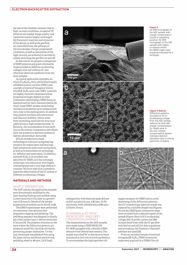
Figure 2 (a) SEM micrograph of the AEZ sample with charge compensation nozzle in operating position. (b) SEM micrograph of the AEZ sample with region of interest where the EBSD maps were acquired indicated by a rectangle.
subsequently with diamond paste (0.3 μm and 0.1 μm particle size, 120 rpm, 2.5 N) and finally with colloidal silica (100 rpm, 2.5 N) for 15 min.
scanning electron microscopy and EBSD ORIENTATION MAPPINGThe measurements on the AEZ samples were made using a ZEISS MERLIN FE-SEM equipped with a Nordlys EBSD detector from Oxford Instruments. The sample was tilted 70° to the electron beam and placed at 14.5 mm of working distance. To accommodate the high specimen tilt
angles necessary for EBSD and to avoid shadowing of the diffraction patterns, the CC’s standard gas injection nozzle was replaced by a suitably shaped one (Figures 1b and 2a). EBSD grain orientation maps were recorded from a selected region of the sample (Figure 2b) at 15 kV accelerating voltage, 0.8 nA probe current and 280 ns pixel dwell time with the CC gas flow switched on and off. For data acquisition and processing, the Flamenco-Channel5 software was used [10].
From an uncoated sample of textured hexagonal b-Si3N4, EBSD orientation maps were acquired in a ZEISS Ultra 55
Figure 3 (below)Diffraction patterns recorded at 15 kV accelerating voltage from the AEZ sample without (a) and with charge compensation (b). Bright spot in the non-charge compensation pattern indicates detector saturation due to strong specimen charging.
electron backscatter diffraction
25MicroscopyandAnalysis | September 2013
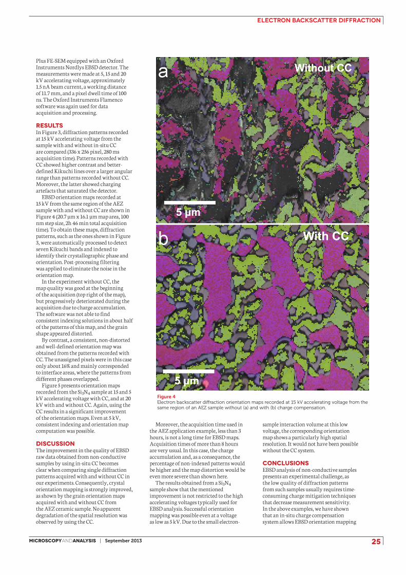
Figure 4 Electron backscatter diffraction orientation maps recorded at 15 kV accelerating voltage from the same region of an AEZ sample without (a) and with (b) charge compensation.
Plus FE-SEM equipped with an Oxford Instruments Nordlys EBSD detector. The measurements were made at 5, 15 and 20 kV accelerating voltage, approximately 1.5 nA beam current, a working distance of 11.7 mm, and a pixel dwell time of 100 ns. The Oxford Instruments Flamenco software was again used for data acquisition and processing.
ResultsIn Figure 3, diffraction patterns recorded at 15 kV accelerating voltage from the sample with and without in-situ CC are compared (336 x 256 pixel, 280 ms acquisition time). Patterns recorded with CC showed higher contrast and better-defined Kikuchi lines over a larger angular range than patterns recorded without CC. Moreover, the latter showed charging artefacts that saturated the detector.
EBSD orientation maps recorded at 15 kV from the same region of the AEZ sample with and without CC are shown in Figure 4 (20.7 μm x 16.1 μm map area, 100 nm step size, 2h 46 min total acquisition time). To obtain these maps, diffraction patterns, such as the ones shown in Figure 3, were automatically processed to detect seven Kikuchi bands and indexed to identify their crystallographic phase and orientation. Post-processing filtering was applied to eliminate the noise in the orientation map.
In the experiment without CC, the map quality was good at the beginning of the acquisition (top right of the map), but progressively deteriorated during the acquisition due to charge accumulation. The software was not able to find consistent indexing solutions in about half of the patterns of this map, and the grain shape appeared distorted.
By contrast, a consistent, non-distorted and well-defined orientation map was obtained from the patterns recorded with CC. The unassigned pixels were in this case only about 16% and mainly corresponded to interface areas, where the patterns from different phases overlapped.
Figure 5 presents orientation maps recorded from the Si3N4 sample at 15 and 5 kV accelerating voltage with CC, and at 20 kV with and without CC. Again, using the CC results in a significant improvement of the orientation maps. Even at 5 kV, consistent indexing and orientation map computation was possible.
DiscussionThe improvement in the quality of EBSD raw data obtained from non-conductive samples by using in-situ CC becomes clear when comparing single diffraction patterns acquired with and without CC in our experiments. Consequently, crystal orientation mapping is strongly improved, as shown by the grain orientation maps acquired with and without CC from the AEZ ceramic sample. No apparent degradation of the spatial resolution was observed by using the CC.
sample interaction volume at this low voltage, the corresponding orientation map shows a particularly high spatial resolution. It would not have been possible without the CC system.
ConclusionsEBSD analysis of non-conductive samples presents an experimental challenge, as the low quality of diffraction patterns from such samples usually requires time-consuming charge mitigation techniques that decrease measurement sensitivity. In the above examples, we have shown that an in-situ charge compensation system allows EBSD orientation mapping
Moreover, the acquisition time used in the AEZ application example, less than 3 hours, is not a long time for EBSD maps. Acquisition times of more than 8 hours are very usual. In this case, the charge accumulation and, as a consequence, the percentage of non-indexed patterns would be higher and the map distortion would be even more severe than shown here.
The results obtained from a Si3N4 sample show that the mentioned improvement is not restricted to the high accelerating voltages typically used for EBSD analysis. Successful orientation mapping was possible even at a voltage as low as 5 kV. Due to the small electron-
electron backscatter diffraction
26 September 2013 | MicroscopyandAnalysis
biography Sonia Serrano-Zabaleta received her degree in engineering in 2010 and her Masters in physics in 2011. Now a PhD student at the Institute of Materials Science of Aragon (CSIC-U. Zaragoza, Spain), she works on the elaboration of directionally solidified eutectics and the characterization of their interfaces by means of electron backscatter diffraction and high resolution electron microscopy.
abstractElectron backscatter diffraction (EBSD) is a powerful technique for structural characterization of micro- or nanocrystalline samples in the scanning electron microscope (SEM). Reliable EBSD analysis of non-conductive samples has so far required the use of conductive coatings or variable pressure (VP) SEM. An in-situ charge compensation system provides improved EBSD analysis of nonconductive samples without the drawbacks of these conventional methods. Similar to VP-SEM, charge neutralisation is achieved by gas ionization, but at negligible loss of resolution due to a significantly reduced interaction volume of beam and backscattered electrons with gas particles.
acknowledgementsAngel Larrea and Sonia Serrano-Zabaleta acknowledge funding from project MAT2012-30763 and the use of Servicio General de Apoyo a la Investigación-SAI, Universidad de Zaragoza. The AEZ sample was kindly provided by M. C. Mesa.
Corresponding author details Dr Heiko Stegmann,Carl Zeiss Microscopy GmbH,Training, Application and Support Center (TASC),Carl-Zeiss-Strasse 22, 73447 Oberkochen, GermanyTel: +49 151 4676 1714Email: [email protected]
Figure 5 Electron backscatter diffraction orientation maps recorded in the marked areas of a Si3N4 sample without (a) and with (b, c and d) charge compensation at different accelerating voltages.
of insulating, nanocrystalline samples without special sample preparation or further countermeasures to eliminate specimen charging. The pattern contrast and quality obtained with the CC system is comparable to those from conductive samples and good enough to ensure phase discrimination and accurate crystallographic orientation.
The restrictions of sample coating or using VP-SEM also apply to energy dispersive X-ray spectroscopic (EDS) analysis of non-conductive samples. It can be improved by in-situ CC as well [4]. Using it for simultaneous EDS and EBSD analysis to couple crystallographic and chemical information enables unambiguous phase identification of insulating materials.
Clean sample surfaces are an essential requirement to successful EBSD analysis. The CC system provides the additional benefit of being able to remove carbon contamination in-situ from the specimen surface [11]. To this end, the region of interest is flooded with oxygen instead of nitrogen, while being exposed to the electron beam. Thus, cleaning of the sample before loading is avoided, and its surface can be repeatedly cleaned whenever necessary between EBSD measurements.
References1. Reimer, L. Scanning Electron Microscopy, Springer, Germany, 1998.2. Zaefferer, S. et al. Three-Dimensional Orientation Microscopy in a Focused Ion
Beam-Scanning Electron Microscope: A New Dimension of Microstructure Characterization. Metallurgical and Materials Transactions 39A:374-389, 2008.3. El-Dasher, B. S., Torres, S. G. In: Electron Backscatter Diffraction in Materials Science 2, LLNL-Book-405556, 2008.4. Stodolka, J., Albiez, M. Local Charge Compensation, Carl Zeiss Microscopy White Paper, 2010.5. Serrano-Zabaleta, S. et al. Orientation relationships and interfaces in directionally solidified eutectics for solid oxide fuel cell anodes. Journal of the European Ceramic Society, http://dx.doi.org/10.1016/j.jeurceramsoc.2013.06.0086. Llorca, J. and Orera, V. M. Directionally-solidified eutectic ceramic oxides. Progress in Materials Science 51:711-809, 2006.7. Oliete, P. B. et al. Ultra-High Strength Nanofibrillar Al2O3-YAG-YSZ Eutectics. Advanced Materials 19:2313-2318, 2007.8. Mesa, M. C. et al. Directionally Solidified Al2O3 - Er3Al5O12 - ZrO2 Eutectic Ceramics with Interpenetrating or Nanofibrillar Microstructure: Residual Stress Analysis. Journal of the American Ceramic Society 95(3):1138-1146, 2012.9. Wilkinson, A. J. and Britton, T. B. Strains, planes, and EBSD in materials science. Materials Today 15:166-176, 2012.10. Channel 5. Oxford Instruments HKL. HKL Technology 2006. Denmark.11. Stodolka, J., Bühler, W. In-situ Sample Cleaning, Carl Zeiss Microscopy White Paper, 2008.


![Electron backscatter diffraction in materials characterization 15 01.pdf · 1 Processing and Application of Ceramics 6 [1] (2012) 1–13 Electron backscatter diffraction in materials](https://static.documents.pub/doc/80x56/5f0ff30b7e708231d446b09d/electron-backscatter-diffraction-in-materials-15-01pdf-1-processing-and-application.jpg)


