Electron Induced Surface Reactions of Organometallic Metal(hfac)2Precursors and Deposit PurificationSamantha G. Rosenberg, Michael Barclay, and D. Howard Fairbrother*
Department of Chemistry, Johns Hopkins University, Baltimore, Maryland 21218, United States
*S Supporting Information
ABSTRACT: The elementary processes associated withelectron beam-induced deposition (EBID) and post-deposi-tion treatment of structures created from three metalII(hfac)2organometallic precursors (metal = Pt, Pd, Cu; hfac =CF3C(O)CHC(O)CF3) have been studied using surfaceanalytical techniques. Electron induced reactions of adsorbedmetalII(hfac)2 molecules proceeds in two stages. For comparatively low electron doses (doses <1 × 10¹⁷ e−/cm2) decompositionof the parent molecules leads to loss of carbon and oxygen, principally through the formation of carbon monoxide. Fluorine andhydrogen atoms are also lost by electron stimulated C−F and C−H bond cleavage, respectively. Collectively, these processes areresponsible for the loss of a significant fraction (≥50%) of the oxygen and fluorine atoms, although most (>80%) of the carbonatoms remain. As a result of these various transformations the reduced metal atoms become encased in an organic matrix that isstabilized toward further electron stimulated carbon or oxygen loss, although fluorine and hydrogen can still desorb in the secondstage of the reaction under the influence of sustained electron irradiation as a result of C−F and C−H bond cleavage,respectively. This reaction sequence explains why EBID structures created from metalII(hfac)2 precursors in electron microscopescontain reduced metal atoms embedded within an oxygen-containing carbonaceous matrix. Except for the formation of copperfluoride from CuII(hfac)2, because of secondary reactions between partially reduced copper atoms and fluoride ions, the chemicalcomposition of EBID films and behavior of metalII(hfac)2 precursors was independent of the transition metal’s chemical identity.Annealing studies of EBID structures created from PtII(hfac)2 suggest that the metallic character of deposited Pt atoms could beincreased by using post deposition annealing or elevated substrate temperatures (>25 °C) during deposition. By exposing EBIDstructures created from CuII(hfac)2 to atomic oxygen followed by atomic hydrogen, organic contaminants could be abatedwithout annealing.
Electron beam-induced deposition (EBID) of volatile organo-metallic precursors is a vacuum-based, site-selective, single-steplithographic technique capable of making and prototypingthree-dimensional, metal-containing nanostructures in electronmicroscopes without masks or resists.1−4 A number of differentmetals can be deposited using organometallic precursorsdeveloped for thermal deposition processes such as chemicalvapor deposition (CVD), enabling EBID deposits to be tailoredfor particular applications. For example, Pt or Cu containingprecursors (e.g., MeCpPtMe3, (hfac)Cu
I(vinyltrimethylsilane))are preferred for the growth of metallic nanowires or inelectronic applications,5−8 whereas Co or Fe containingprecursors (e.g., Co(CO)3NO, Co2(CO)8 and Fe(CO)5) areused to create magnetic nanostructures.9−13 EBID has alsobeen used to create AFM tips,10,14 catalyst nanoparticles forgrowing CNT’s,15,16 magnetic nano-Hall sensors,11 electricalcontacts,17 and in mask repair.18,19
Every organometallic precursor contains organic ligandsattached to the central metal atom. These ligands can besubdivided into monodentate ligands, such as CO and CH3,that are attached to the central metal atom through a singlemetal−ligand bond, and multidentate ligands, such as
hexafluoroacetylacetonate (hfac; CF3C(O)CHC(O)CF3),which are bonded to the central metal atom through multipleligand−metal bonds. Among the bidentate ligands, hfac is oneof the most widely used because it can form metal−ligandbonds with transition metals that do not form stable carbonyls,such as platinum, palladium, and copper.20 CuII(hfac)2 has beenused in EBID to make deposits for high-performance integratedcircuits in an attempt to combine the selective depositionafforded by EBID with copper’s low-cost and lower electricalresistivity compared to Si or Al.21−23
Despite the relative ease and flexibility of structures that canbe created by EBID, a number of scientific and technologicalchallenges are preventing EBID from reaching its full potentialas a robust tool for nanofabrication. One of the majordrawbacks is the often unacceptably high level of organiccontamination, particularly carbon, contained within thedeposits. This contamination negatively impacts the deposit’sproperties (e.g., by increasing resistivity or decreasing catalyticactivity) and therefore limits the range of potential applications
Received: March 10, 2014Accepted: April 30, 2014Published: April 30, 2014
for metal-containing EBID nanostructures. Ligand decom-position is the principal source of organic contamination inEBID. Thus, although CuII(hfac)2, Pd
II(hfac)2 and PtII(hfac)2can all produce pure metal films in thermal depositionprocesses such as CVD,24 nanostructures created by EBIDfrom hfac-containing precursors exhibit high carbon contentsand correspondingly low metal purity. For example, Luisier etal., have reported nanostructures created from CuII(hfac)2 withvery low metal contents (14% Cu), and a correspondingly highcarbon content (75% C).22 Similarly, Miyazoe et al. reportedthat deposits created by EBID from CuII(hfac)2 exhibit only11−12% Cu content.23 These limitations with existing CVDprecursors have provided the impetus to better understand thefundamental bond breaking processes involved in EBID. Thegoal is to provide information that can be used to design new,EBID specific precursors capable of creating nanostructureswith improved metal content.Given the typically low metal content (often <20%) in EBID
structures, several different approaches have been evaluated fortheir ability to abate the organic contamination. Thesestrategies have included varying the deposition conditions(i.e., changing the current, energy, or dwell time of the electronbeam), and heating the substrate to elevated temperatureseither during or after deposition.1,6,12,25,26 An alternativestrategy has been to expose deposits to reactive species capableof volatilizing organic contaminants.27 For example, Miyazoe etal. reported that when EBID deposits created from CuII(hfac)2were treated with a hydrogen−argon plasma, the Cu contentcould be increased from 11 to 12% to 27%.23 In related studies,Wnuk et al. have observed that when EBID films created fromdimethyl(acetylacetonate)gold(III) (Me2Au(acac)) were ex-posed to atomic oxygen (AO) and then atomic hydrogen(AH), almost all of the carbon was removed, creating pure golddeposits.28
As a step toward developing a more detailed fundamentalunderstanding of the electron stimulated reactions ofmetalII(hfac)2 compounds, Engmann et al., have recentlyexplored the interactions of low energy (0−12 eV) electronswith gas phase CuII(hfac)2, Pd
II(hfac)2.29 Motivation for these
studies derives from the widespread belief that in the EBIDprocess, precursor dissociation is initiated by the low energysecondary electrons produced by the interactions of the high-energy primary beam with the substrate.30,31 These gas phasestudies showed that CuII(hfac)2 predominately undergoesnondissociative electron attachment (NDEA) to formCuII(hfac)2
−, whereas for PdII(hfac)2, the precursor’s preferredreaction pathway is the loss of (hfac)−.29 The authorspostulated that this difference occurs because the open shellCuII(hfac)2 (17 electrons) is more likely to be stabilized by theaddition of an extra electron to form CuII(hfac)2
Over the past several years, we have developed an ultrahighvacuum (UHV), surface science approach to acquire moredetailed molecular level information on the EBID proc-ess.28,32−40 These surface science studies on adsorbed organo-metallic precursors represent an increasing level of complexitycompared to gas phase studies and provide a bridge betweeninformation that can be obtained from typical EBID studies,primarily conducted in electron microscopes, and data on thereactions of electrons with isolated precursor molecules in thegas phase. Thus, UHV surface science studies can track theelectron-stimulated decomposition of organometallic precur-sors in situ, identify the volatile species created during
deposition, and study the effects of post-deposition purificationstrategies. In the present study, we have used this approach tointerrogate the electron stimulated surface reactions of thedifferent metalII(hfac)2 precursors, specifically platinum(II)hexafluoroacetylacetonate (PtII(hfac)2), copper(II) hexafluor-oacetylacetonate (CuII(hfac)2), and palladium(II) hexafluor-oacetylacetonate (PdII(hfac)2). Results from these studies havebeen used to determine the bond breaking processes involvedin deposition and the extent to which these processes aresimilar or differ among the three different precursors. As part ofour investigation, we have also examined the effects of twodifferent post-deposition abatement strategies, specificallysubstrate heating and exposure to atomic radicals, on thebonding and composition in EBID films created fromPtII(hfac)2 and CuII(hfac)2.
CAS 14781−45−4, Strem Chemicals, Inc.), Palladium(II) hexafluor-oacetylacetonate (PdII(hfac)2; CAS 64916−48−9, Strem Chemicals,Inc.), and Platinum(II) hexafluoroacetylacetonate (PtII(hfac)2; CAS65353−51−7, Strem Chemicals, Inc.) exist as blue, yellow, and orangecrystals, respectively, at standard temperature and pressure (STP). Allthree precursors were added into glass fingers that were attached to agas manifold. Each precursor was admitted into the two UHVchambers after the gas manifold had been evacuated into the mTorrpressure regime by a mechanical pump and the precursor subsequentlyheated to ≈50−70 °C.
Two types of experiments were conducted in two different UHVchambers, whose analytical capabilities have been described inprevious publications.32,34,38,40,41 The bulk of the experiments reportedin this study were carried out in situ with X-ray photoelectronspectroscopy (XPS) and mass spectrometry (MS) to study the effectof electron irradiation on adsorbed PtII(hfac)2, CuII(hfac)2 andPdII(hfac)2 molecules as well as the effect of annealing on EBIDstructures created from PtII(hfac)2. The second UHV chamber, an AESsystem (PHI 610) modified by the addition of a thermal cracker wasused to study the composition of films grown by EBID fromCuII(hfac)2, Pd
II(hfac)2 and PtII(hfac)2 under steady-state depositionconditions as well as the effect of atomic radicals on EBID structurescreated from CuII(hfac)2.
Brief descriptions of the various experimental elements are providedin the following sections.
XPS/MS Experiments. Creating Films. Films of nanometerthicknesses were created on 1 cm2 substrates by introducing theprecursor gases onto cooled 1 cm2 substrates with no electronirradiation present. The average thicknesses of the films created fromthe precursor in this way were, CuII(hfac)2 (2.0−2.5 nm), PdII(hfac)2(>5.0 nm), and PtII(hfac)2 (3.8−4.2 nm). Experiments with PtII(hfac)2were conducted on a Au substrate cooled to −168 °C, while studies onCuII(hfac)2 and PdII(hfac)2 were conducted on an amorphous carbon(a:C) substrate (created by Ar+ sputtering HOPG) cooled to −110°C. For CuII(hfac)2 and PdII(hfac)2 experiments were performed ona:C because there was evidence that these two molecules underwentpartial decomposition on Au. For example, in the case of CuII(hfac)2,metallic Cu peaks were observed in the XPS even at low depositiontemperatures, consistent with previous studies by Lin et al.42
PtII(hfac)2 was preferred for detailed XPS analysis because ofspectroscopic issues with PdII(hfac)2 and CuII(hfac)2. In the case ofPdII(hfac)2, this was due to overlap between the Pd(3p3/2) and O(1s)peaks,43 whereas for CuII(hfac)2, unambiguous deconvolution of theCu(2p) region is extremely difficult. However, a sufficient number ofcomplementary experiments were performed with PdII(hfac)2 andCuII(hfac)2 to allow us to compare the reactivity among the threeMII(hfac)2 precursors.
For XPS experiments on PtII(hfac)2, film thicknesses weredetermined by measuring the attenuation of the Au(4f) signal.44
CuII(hfac)2 film thicknesses on the a:C substrates were determined
ACS Applied Materials & Interfaces Research Article
from the attenuation of the C−C peak associated with the a:Csubstrate. The more limited number of experiments performed withPdII(hfac)2 were conducted on sufficiently thick (>5.0 nm) films thatthere was no longer a contribution to the C(1s) spectra from the a:Csubstrate.38,40,41
Electron Source. Once the film’s thickness and composition weredetermined by XPS, it was exposed to a known electron dose orientedat normal incidence to the sample surface. For all MS and XPSexperiments a commercial flood gun (Specs FG 15/40) was used as abroad beam electron source.34,38 An incident electron energy of 500eV was used throughout, calculated from the sum of the electronenergy generated by the flood gun (480 eV) and a positive bias (+20V) applied to the substrate to prevent the majority of secondaryelectrons produced during irradiation from escaping. The targetcurrent was held at 5 μA, unless noted. Electron irradiation is reportedin terms of dose (e−/cm2).AES Experiments. Creating EBID Films. The metalII(hfac)2
precursor was directed onto the substrate through a directionaldoser, while the Auger electron beam was rastered across the surfacefor a prescribed period of time. The pressure of precursor molecules atthe surface was held constant during deposition by monitoring thechamber pressure, as was the target current. Film thicknesses were notmeasured, but each deposit was sufficiently thick to obscure the AESsignal from the underlying Au substrate. To ensure that deposition wasdefined by the electron beam (i.e., it was created by EBID), the two-dimensional nature of the films was checked using a secondaryelectron detector (SED).Electron Source. For all AES experiments a 3 keV electron beam
was created from a LaB6 filament cathode and rastered over ≈1.5 μmspot size and a power density of ∼2 × 10² μW/μm2.Radical Treatment. The effect of atomic radicals on EBID
structures created from CuII(hfac)2 was studied in situ. Atomic
radicals were generated by flowing oxygen or hydrogen gas through athermal gas cracker (Oxford Applied Research) to produce a directedflux of atomic radicals (80−90% dissociation efficiency based onmanufacturer’s estimate).28
The chemical composition of EBID films was determined by AES.Using the AugerMap software, spatial concentration maps of surfacecopper, carbon, fluorine, and oxygen atoms were also obtained bymeasuring the difference in AES signals between their respective Augertransitions (CuLMM ≈ 920 eV, CKLL ≈ 262 eV, FKLL ≈ 647 eV,OKLL ≈ 503 eV) and a proximate electron energy that correspondedto the background signal.
3. RESULTS
Figure 1 shows the evolution in the Pt(4f), C(1s), O(1s), andF(1s) regions measured by XPS for 3.6−4.2 nm thickPtII(hfac)2 films as a function of increasing electron dose.Control studies (shown in Figure S1 in the SupportingInformation) used to determine the sensitivity of the adlayerto the secondary electrons generated during XPS analysisrevealed that 161 min of total X-ray exposure produce relativelysmall changes to the Pt(4f), C(1s), O(1s) regions, most notablya loss in the CF3 group intensity and a slight broadening of theC(1s) region. Despite this relative insensitivity, each film wasonly exposed to X-ray irradiation after deposition and thenagain after a single electron dose, collectively corresponding toa total of ∼70 min of X-ray exposure. Thus, changes in the XPSshown in Figure 1 are dominated by the effect of the 500 eVelectrons generated by the electron gun.
Figure 1. Evolution of the Pt(4f), C(1s), O(1s), and F(1s) XP regions for 3.6−4.2 nm thick films of PtII(hfac)2 as a function of increasing electrondose. Films were adsorbed onto a gold substrate at −168 °C and the incident electron energy was 500 eV. The corresponding electron dose is shownon the right-hand side of each set of spectra. Fits are included in the Pt(4f) region for the parent (red, dashed lines) and product (blue, dotted lines)species. All XP spectra were recorded with a step size of 0.125 eV and at pass energies of 22 eV.
ACS Applied Materials & Interfaces Research Article
Analysis of the evolution in Pt(4f), C(1s), O(1s), and F(1s)regions exposed to electron radiation and correspondingchanges to the atom concentration (see Figure 2) reveals two
regimes of transformation; those that occur for electron doses≤1 × 10¹⁷ e−/cm2 and then for ≥1 × 10¹⁷ e−/cm2. Prior toirradiation, the Pt(4f) region contains a Pt(4f7/2/4f5/2) doublet(Pt(4f7/2) peak position = 74.3 eV) associated with adsorbedPtII(hfac)2 molecules (shown as dashed lines in Figure 1). Forelectron doses ≤1 × 10¹⁷ e−/cm2, the Pt(4f) region broadens toa lower binding energy and the resulting envelope can be wellfit using contributions from parent PtII(hfac)2 molecules and anew Pt(4f7/2/4f5/2) doublet with a Pt(4f7/2) peak at 72.6 eV.This new component is indicated by dotted lines in Figure 1with the Pt(4f7/2) peak identified at Ptred. For electron doses ≥1× 10¹⁷ e−/cm2, the Pt(4f) spectral envelope is dominated bythe Ptred species with little or no contribution from thePt(4f7/2/4f5/2) doublet associated with the parent PtII(hfac)2molecules. The decrease (>1.5 eV) that occurs to the Pt(4f)binding energy as a result of electron irradiation is mostapparent by comparing the bottom two spectra in Figure 6a,which shows the measurable change in Pt(4f) binding energythat occurs as the Pt(4f7/2/4f5/2) molecules are decomposed byelectron irradiation.
The C(1s) region prior to electron exposure consists of threewell-defined peaks, centered at 285.5, 288.5, and 293.6 eV, dueto the CH, CO and CF3 carbon atoms in the hfac ligand,respectively.21 For electron doses <1 × 10¹⁷ e−/cm2, the well-defined peak structure is degraded and the CF3 peak disappears.For electron doses >1 × 10¹⁷ e−/cm2, the dominanttransformation is an increase in concentration of the graphiticlike CC/CH2 species at the expense of the CF and CO species(see also Figure S2 in the Supporting Information for the effectof electron irradiation on PdII(hfac)2 films), although theintegrated area of the C(1s) region decreases by only 10−20%over the course of electron exposure. Consequently, thedominant transformation that occurs to carbon atoms involveschanges to the local bonding environments as opposed todesorption. Prior to irradiation, the O(1s) region consists of adominant peak at 534.5 eV due to the CO species in the hfacligand.21 For electron doses ≤1 × 10¹⁷ e−/cm2, changes in theO(1s) region are dominated by a loss of ∼50% spectralintensity while for electron doses ≥1 × 10¹⁷ e−/cm2 theintensity in the O(1s) region remains relatively unchanged (seeFigure 2(a)). Initially, the F(1s) region also consists of a singlepeak (at 689.3 eV) due to the CF3 species in the hfac ligand.21
For electron doses ≤1 × 10¹⁷ e−/cm2, there is a pronouncedloss of intensity (∼50%) and a small decrease in bindingenergy. At higher electron doses ≥1 × 10¹⁷ e−/cm2, the F(1s)region continues to lose intensity, albeit at a slower rate (Figure2b).Figure 3a shows a comparison of the neutral gas phase
species produced when, (i) gas phase PtII(hfac)2 moleculeswere exposed to 70 eV electrons in the quadrupole MS and, (ii)adsorbed PtII(hfac)2 molecules were irradiated by 500 eVelectrons. Analysis of Figure 3a,i reveals that the MS of gasphase PtII(hfac)2 yields significant peaks for CF3, CO, F, O, andC, with smaller contributions from CF2, CFO, CO2, and H2.Although the authors were not able to find any mass spectradata for the PtII(hfac)2 precursor, the cracking pattern in Figure3a is analogous to published mass spectra data on theCuII(hfac)2 precursor.
45 Figure 3a,ii shows that when adsorbedPtII(hfac)2 molecules are electron irradiated, the volatileneutrals produce significant peaks for CO, O, C, and H2,with smaller contributions from CO2. Indeed, the ratio ofCO:O:C is consistent with the fragmentation pattern for CO.Therefore, a notable contrast to the gas phase PtII(hfac)2spectra in Figure 3a,i is that no fluorine-containing species(e.g., CF3, CF2,, CFO, etc.) are observed in Figure 3a,ii. Figure3b shows the kinetics of electron stimulated CO evolution fromadsorbed PtII(hfac)2 molecules (solid circles - left-hand axis).Figure 3b also shows how the fractional concentration ofoxygen atoms volatilized from PtII(hfac)2 during electronirradiation changes as a function of electron dose. BecauseFigure 2a shows that ∼50% of the nascent oxygen atoms arelost from adsorbed PtII(hfac)2 films as a result of electronirradiation, this is plotted as (O/O0 − 0.5) (left-hand axis−open circles). Analysis of Figure 3b shows that the gas phaseCO evolution and loss of oxygen from the surface follow thesame kinetic dependence on electron dose.Figure 4 details the effect of electron exposure on the F(1s)
XP region of a CuII(hfac)2 film. Prior to electron irradiation, theF(1s) region, is characterized by one peak at 688.6 eV,consistent with Figure 1. However, in contrast to the evolutionof the F(1s) region of PtII(hfac)2 or PdII(hfac)2 films thedecrease in C−F peak intensity that occurs with increasing
Figure 2. Change in the fractional coverage of adsorbed (a) oxygenand (b) fluorine atoms for 3.6−4.2 nm PtII(hfac)2 films exposed toelectron irradiation, plotted as a function of electron dose. Eachrelative concentration (F/F0, O/O0) was determined by XPS with theinitial F0, and O0 values measured on the PtII(hfac)2 film prior toelectron irradiation. Films were adsorbed onto Au substrates at −168°C and exposed to 500 eV electrons.
ACS Applied Materials & Interfaces Research Article
electron dose is accompanied by the appearance of a distinctnew peak at 686.0 eV, indicative of a fluoride ion (F−).46
Figure 5a−c shows the in situ AE spectra of 500 μm × 360μm structures deposited by EBID in the AES system using aconstant partial pressure of (a) CuII(hfac)2, (b) Pd
II(hfac)2, and(c) PtII(hfac)2 (PM(hfac)2 ≈ 1.5−3.0 × 10⁻⁷ Torr). Figure 5a−cshow that the Auger spectra contain transitions associated withtheir respective metals: Cu (920 eV, 849 eV, 776 eV), Pd (330eV) and Pt (64 eV). A discernible oxygen peak (503 eV) is alsopresent but all of the Auger spectra are dominated by a largecarbon (272 eV) peak. The most significant difference betweenthe three structures is that the Cu II(hfac)2 displays a prominent
F peak (647 eV), which is noticeably absent for the PtII(hfac)2and barely visible for PdII(hfac)2.Figure 6 shows the effect of annealing an EBID film initially
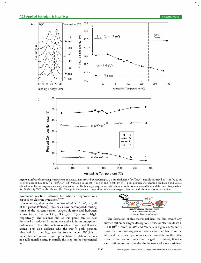
created by exposing PtII(hfac)2 molecules to an electron dose of4.50 × 1017 e−/cm2. On the basis of the data in Figure 1 thiselectron dose is sufficient to decompose all of the parentPtII(hfac)2 molecules, but insufficient to remove all of thenascent fluorine atoms. Figure 6a describes the effect ofelectron irradiation and subsequent annealing on the Pt(4f7/2)peak position. The initial electron dose used to generate theEBID structure causes the Pt(4f7/2) peak position to decreaseby 1.7 eV, from 74.3 to 72.6 eV, as shown in Figure 1. Whenthe film is subsequently annealed to room temperature the
Figure 3. (a) Mass spectrum (0−100 amu) of (i) gas phase PtII(hfac)2 measured at PPt(hfac)2 ≈ 6.0 × 10⁻⁷ Torr, (ii) the volatile neutral speciesproduced when a ∼ 4.0 nm film of PtII(hfac)2, adsorbed onto a gold substrate at −168 °C was irradiated by an electron dose of 2.40 × 10¹⁷ e−/cm2
(incident energy of 500 eV); the spectrum represents an average of MS taken every 20 s during the electron exposure. (b) Effect of electron dose on(filled circles) partial pressure of gas phase CO evolved from a PtII(hfac)2 film, (open circles) change in the labile oxygen atom concentration in thefilm (O/O0 − 0.5). Both data sets were acquired for 3.6−4.2 nm PtII(hfac)2 films (incident electron energy 500 eV).
ACS Applied Materials & Interfaces Research Article
Pt(4f7/2) peak position remains unchanged although at higherannealing temperatures the Pt(4f7/2) peak systematicallydecreases, reaching a binding energy of 71.6 eV at 367 °C.This value is close to that of bulk platinum (71.2 eV).43 Figure6b shows the variation in intensity within the Pt(4f), C(1s),F(1s), and O(1s) regions of the EBID film as a function ofannealing temperature. The platinum, carbon and fluorinesignals remain unchanged. The oxygen signal, however,decreases steadily above 120 °C and is barely perceptible(<5%) at annealing temperatures above 300 °C.Figure 7a−c show the in situ AE spectra of: (a) a rectangular
EBID structure deposited in the AES system from CuII(hfac)2,
(b) the same structure after 40 h exposure to atomic oxygenand (c) subsequently exposed to 2 h of atomic hydrogen.Figure 8 shows the corresponding AES maps. Figures 7a and 8ashow that the native EBID structure is characterized by thepresence of: Cu (920, 849, 776 eV), C (272 eV), O (503 eV),and F (647 eV) Auger peaks. Following 40 h of atomic oxygenexposure, the carbon and fluorine has all but disappeared with aconcomitant increase in intensity of the oxygen and copperAES peaks (Figures 7b and 8b). After this structure wassubsequently exposed to atomic hydrogen for 2 h, the oxygensignal decreased drastically, with a corresponding increase inthe Cu AES signal (Figures 7c and 8c). The combination ofatomic oxygen followed by atomic hydrogen treatmenttherefore produces a structure dominated by Cu AES peaks.
4. DISCUSSIONElectron Stimulated Reactions. Figures 1−3 show that
electron irradiation of adsorbed PtII(hfac)2 molecules changesthe chemical composition and/or bonding environment for theplatinum, carbon, fluorine, and oxygen atoms. The majority ofchanges in bonding and atom concentration occur for electrondoses <1 × 10¹⁷ e−/cm2. These include the loss of parentPt(+2) species from PtII(hfac)2 into a more reduced form ofplatinum (Ptred) which exhibits a binding energy (72.6 eV)intermediate between Pt atoms in PtII(hfac)2 and metallic Pt (≈71.2 eV).43 Similar changes in Pt(4f7/2) binding energies havealso been observed for other Pt precursors, MeCpPtMe3 andPt(PF3)4, exposed to electron irradiation.32,38 The loss ofsignificant amounts of both oxygen and fluorine from thesurface also occurs during this initial period of irradiation.Indeed, all of the oxygen loss (≈ 50% of the initial content)occurs for electron doses <1 × 10¹⁷ e−/cm2. Moreover, Figure3b shows that there is a correlation between the rate at whichvolatile oxygen atoms are lost from the surface and the rate ofgas phase CO production. From this, we conclude that oxygenis lost predominantly in the form of CO(g), possiblyaccompanied by a small amount of CO2(g) (see Figure 3).Based on the chemical structure of the hfac ligands (CF3C-(O)CHC(O)CF3), it appears that approximately half of theCO groups in the precursor molecules are ejected into thegas phase. The concomitant loss of fluorine atoms from the filmis evidenced by the decrease in the F(1s) peak intensity and theCF3 peak in the C(1s) envelope, shown in Figures 1 and 2b.However, the loss of fluorine from the surface is notaccompanied by the appearance of any fluorine or carbon−fluorine containing fragments (e.g., F, CF, CFO) in the neutralgas phase species ejected during the electron irradiation ofPtII(hfac)2 films (Figure 3a(ii)). This suggests that fluorineatoms desorb predominantly in the form of F−(g) because ofelectron-stimulated C−F bond cleavage (C−F(ads) + e− ⇒ C·(ads) + F−(g)), a process that has been shown to be importantfor fluoropolymers or fluorine-containing thin films (e.g.,SAMs) exposed to electrons or ionizing radiation.47−52 Becauseelectron-stimulated C−F bond cleavage does not result in anycarbon desorption, CO and possibly CO2 are the only volatilecarbon-containing species produced. These observationsexplain why electron irradiation leads to significant losses ofoxygen and fluorine atoms from the film, but only acomparatively small change in the carbon content. AlthoughXPS cannot detect hydrogen atoms, the significant increase inintensity of the gas phase m/z = 2 peak (Figure 3a(ii)) duringelectron irradiation indicates that hydrogen is lost from the filmas H2(g) because of electron-stimulated C−H bond cleavage, a
Figure 4. Evolution of the F(1s) XP region as a function of electrondose for 2.0−2.5 nm thick films of CuII(hfac)2 adsorbed onto an (a:C)substrate at −100 °C (dose shown on right-hand side).
Figure 5. Auger electron spectra of EBID structures created from (a)CuII(hfac)2, (b) PdII(hfac)2, and (c) PtII(hfac)2 on a Au substrate.Deposition conditions were Pprecursor ≈ 1.5- 3.0 × 10⁻⁷ Torr, incidentbeam energy =3 keV, substrate current ≈1- 2 μA for a total electrondose of: ∼ 4.7 × 10¹⁸ e−/cm2. Inset shows an SEM image of thePtII(hfac)2 structure.
ACS Applied Materials & Interfaces Research Article
prominent reaction pathway for adsorbed hydrocarbonsexposed to electron irradiation.53−59
In summary, after an electron dose of ∼1 × 10¹⁷ e−/cm2, allof the parent PtII(hfac)2 molecules have decomposed, causingsome of the nascent carbon, oxygen, fluorine and hydrogenatoms to be lost as CO(g)/CO2(g), F−(g) and H2(g),respectively. The residual film at this point can be bestdescribed as reduced Pt atoms encased within an amorphouscarbon matrix that also contains residual oxygen and fluorineatoms. This also explains why the Pt(4f) peak positionobserved for the Ptred species formed when PtII(hfac)2molecules decompose is not representative of platinum atomsin a fully metallic state. Pictorially this step can be representedas
The formation of this matrix stabilizes the film toward anyfurther carbon or oxygen desorption. Thus, for electron doses >∼1 × 10¹⁷ e−/cm2 the XPS and MS data in Figures 1, 2a, and 3show that no more oxygen or carbon atoms are lost from thefilm, and the reduced platinum species formed during the initialstage of the reaction remain unchanged. In contrast, fluorinecan continue to desorb under the influence of more sustained
Figure 6. Effect of annealing temperature on a EBID film created by exposing a 3.30 nm thick film of PtII(hfac)2 initially adsorbed at −168 °C to anelectron dose of 4.50 × 10¹⁷ e−/cm2. (a) (left) Variation in the Pt(4f) region and (right) Pt(4f7/2) peak position after electron irradiation and also asa function of the subsequent annealing temperature; in the binding energy of metallic platinum is shown as a dashed line, and the onset temperaturefor PtII(hfac)2 CVD is also shown. (b) Change in the percent composition of carbon, oxygen, fluorine, and platinum atoms in the film.
ACS Applied Materials & Interfaces Research Article
electron irradiation as a result of C−F bond cleavage and F−
ejection. This transformation accounts not only for thesustained loss of signal in the F(1s) region for electron doses> ∼1 × 10¹⁷ e−/cm2, but also the corresponding changes in theC(1s) region (Figure 1 and Figure S2 in the SupportingInformation) as CF2 and CF species are converted intographitic-like, C(ads), species. This second step can berepresented as
Analogous low-temperature UHV studies conducted withPdII(hfac)2 and CuII(hfac)2 reveal that similar transformationsoccur as a result of electron irradiation, with the loss of fluorineand oxygen, CO(g) evolution, and reduction of the metalatoms. For example, Figure S2 in the Supporting Informationshows that the evolution of the C(1s) region for PdII(hfac)2exposed to electron irradiation is qualitatively similar to thechanges observed for PtII(hfac)2 (see Figure 1). Anotherexample is the nature of the gas phase species produced whenadsorbed CuII(hfac)2 molecules were exposed to electronirradiation (compare Figure S3 in the Supporting Informationand Figure 3a,ii). The one notable difference between the threemetalII(hfac)2 complexes is the Cu
II(hfac)2 precursor, where theelectron stimulated loss of C−F bonds in the F(1s) region wasaccompanied by the appearance of a distinct new peak that canbe identified as a fluoride ion (Figure 4).33,46 The appearance ofa fluoride (F−) species can be understood by considering thatelectron irradiation of adsorbed CuII(hfac)2 molecules createsreduced Cu species while at the same time also liberatingreactive F− ions from C−F bond cleavage. Reactions between
Figure 7. Auger electron spectra of (a) an EBID structure createdfrom CuII(hfac)2 on a Au substrate. Deposition conditions werePCu(hfac)2 ≈ 1.0 × 10⁻⁷ Torr, incident beam energy = 1.5 keV, substrate
current ≈ 4.4 μA, deposition time 1 h; (b) the deposited structureexposed to 40 h of atomic oxygen, and then (c) exposed to 2 h ofatomic hydrogen.
Figure 8. Auger electron elemental maps of (a) EBID films createdfrom CuII(hfac)2 on a Au substrate; deposition conditions werePCu(hfac)2 ≈ 1.0 × 10⁻⁷ Torr, incident beam energy =1.5 keV, substratecurrent ≈ 4.4 μA, deposition time 1 h (b) the deposited film exposedto 40 h of atomic oxygen and then, (c) exposed to 2 h of atomichydrogen.
ACS Applied Materials & Interfaces Research Article
these two species produce a stable copper fluoride. In contrastto Cu, Pd and Pt do not form stable fluorides, providing arationale for the lack of fluoride ion formation in Figure 1.60
This behavior of CuII(hfac)2 in the low-temperature UHVsurface science also explains why there is a pronounced fluorinesignal in the EBID structures created in the AES under steadystate deposition conditions from CuII(hfac)2, a feature that is allbut absent in the deposits created from PdII(hfac)2 andPtII(hfac)2 (Figure 5).An important difference between the EBID structures
created from CuII(hfac)2, PdII(hfac)2, and PtII(hfac)2 in the
AES system (Figure 5) and the films created in the lowtemperature UHV studies is that the AES deposits have beensubjected to much higher effective electron doses. This is aconsequence of the much higher electron flux (∼1 × 10⁴)generated by the Auger electron gun (∼ 2 × 10² μA/mm2)compared to the broad beam electron source used in the UHVsurface science experiments (∼1 × 10⁻² μA/mm2). Thus, if weextrapolate the XPS data shown in Figure 2 to the deposit thatwould form if a film were exposed to orders of magnitudegreater electron fluxes, we would predict that EBID structurescreated in the AES system from PdII(hfac)2, and PtII(hfac)2would contain significant amounts of carbon contamination,along with some oxygen. However, there would be little or nofluorine due to electron stimulated C−F cleavage. This is inqualitative agreement with the chemical composition of thestructures made in the AES system, from PdII(hfac)2 (6.5% Pd,2.7% O, and 90.8%C) and PtII(hfac)2 (3.8% Pt, 4.3% O, and91.9% C), shown in Figure 5. As noted in the previousparagraph the presence of fluorine in films created fromCuII(hfac)2 is due to the formation of copper fluoride.The similarity in the chemical composition of the EBID
structures created from the three metalII(hfac)2 precursors,particularly the comparable concentrations of carbon andoxygen, combined with the observation that the same volatilespecies are detected during electron irradiation, provide strongsupport for the idea that the same overall deposition processesis operative for all three metalII(hfac)2 precursors. In contrast toprevious studies on organometallic complexes that only containmonodentate ligands (e.g., Pt(PF3)4, W(CO)6, and MeCpP-tIVMe3), there is no evidence of direct ligand (hfac) ejectionfollowing electron irradiation. The absence of hfac desorptioncan be inferred not only from the absence of any fluorinecontaining species in the neutrals detected by the QMS duringirradiation (Figure 3), but also by the comparative lack ofchange in the C(1s) XPS area during irradiation and also fromthe preponderance of carbon in deposits created from themetalII(hfac)2 complexes in the AES (Figure 5) and in previousEBID studies using CuII(hfac)2.
21−23,61
The absence of any significant hfac desorption and thesimilar behavior of the three metalII(hfac)2 precursors differsfrom recent gas-phase studies on CuII(hfac)2 and Pd
II(hfac)2. Inthese studies, the nature of the transition metal and theelectronic structure of the complex has been shown to influencethe electron interactions with metalII(hfac)2 complexes,including the potential for hfac ligand desorption.29 Theapparent discrepancy between these studies is a reflection of theimportant role that the surface can play in influencing theoverall sequence of events that accompany EBID. The absenceof any significant hfac desorption in this investigation and inrelated EBID studies can likely be attributed at least in part tothe molecular weight of the hfac fragment (204 amu), which isgreater than any of the central metal atoms (Cu, Pt, Pd). This
kinematic effect will reduce the nascent velocity of any hfacligand released in a bond dissociation process and the ease withwhich it can “escape” from the surface and into the gas phase.Any hfac ligands released from metalII(hfac)2 complexes arealso likely to experience significant interactions with theunderlying substrate through one or both of the coordinatelyunsaturated oxygen atoms. Thus, hfac ligands that thermallydissociate from PdII(hfac)2 on copper surfaces at lowtemperatures (approximately −150 °C) have been shown toremain thermally stable at 100 °C.42 In contrast, hfac ligandsreleased from metalII(hfac)2 complexes in the gas phase will notexperience any of these secondary effects that must beconsidered in a more condensed phase medium. Unfortunately,the inability of the hfac ligands to desorb means that we cannotdirectly compare our results to the related gas-phase studies29
on the same molecules to determine the role and/or relativeimportance of the secondary versus the primary electrons ininitiating precursor decomposition. However, although ourresults do not allow us to unambiguously identify the initialbond dissociation event that causes the various metalII(hfac)2complexes to decompose this lack of information is largelyirrelevant as the fate of the carbon, oxygen, hydrogen, andfluorine atoms is effectively a consequence of how surfacebound hfac ligands decompose under the influence of electronirradiation. We anticipate that a similar situation will beoperative for other bulk multidentate ligands such as acac(CH3COCHCOCH3) and e t h y l e n ed i am i ne(NH2CH2CH2NH2), with the ejection of only small organicfragments during EBID. In support of this assertion, CO andCH4/CH3 were the only volatile carbon-containing fragmentproduced when adsorbed Me2Au(acac) molecules wereelectron irradiated.39 The one aspect of the dissociation/deposition process where the central metal atom does seem toplay a role is in the secondary reactions that can occur betweenthe partially reduced metal atoms liberated in the initialdecomposition step and volatile fragments generated as theligands decompose.
Post-deposition Abatement. In this study, we alsoevaluated the effect of two post-deposition abatementstrategies, annealing and exposure to atomic radicals, on thechemical composition of and bonding in EBID structurescreated from metalII(hfac)2 precursors.Figure 6 shows the effect of annealing an EBID film initially
created from PtII(hfac)2 at −168 °C. On the basis of the initialelectron dose (4.50 × 10¹⁷ e−/cm2) this film is initiallycomposed of reduced platinum atoms, encased in a carbonmatrix that also contains some residual oxygen and fluorineatoms. Figure 6b shows that oxygen is lost (from 11 atomic %to 3 atomic %) when the substrate is annealed above 100 °C.However, increasing the substrate temperature produced nochange in the carbon or fluorine content. For fluorine this incontrast to the effect of electron irradiation due to the fact thatwhile C−F bonds are labile toward electrons they are thermallyinert (C−F bond strength ≈ 490 kJ/mol).20 Increasing thesubstrate temperature above room temperature is also seen toproduce a systematic decrease in the Pt(4f7/2) binding energy(Figure 6a), indicative of the platinum atoms becoming moremetallic. The correlation between the loss of oxygen from thefilm that occurs upon annealing (Figure 6b) and the decrease inPt(4f7/2) binding energy (Figure 6a) suggests that Pt−O bondsare initially present in the as deposited structures. Thispossibility is reasonable given the presence of M−O bonds inthe parent metalII(hfac)2 molecules. Moreover, the loss of
ACS Applied Materials & Interfaces Research Article
oxygen between 0−400 °C is in line with the thermal stabilityof Pt−O bonds formed on Pt nanoparticles.62 Previous studieson EBID deposits formed from MeCpPtMe3, however, havealso reported a decrease in Pt(4f7/2) binding energy of a similarmagnitude to the one shown in Figure 6 and over a similartemperature range in a situation where no Pt−O bonds couldbe present.36 In this case, the decrease in platinum bindingenergy was attributed to the effect of metal atom coalescencepromoted by increased metal atom diffusion in the carbona-ceous matrix at higher substrate temperatures. Our results donot allow us to say unambiguously if one or both of these twoeffects (Pt−O bond cleavage or metal atom coalescence) isresponsible for the decrease in Pt binding energy, althoughFigure 6 demonstrates that increasing the substrate temperatureduring EBID or post deposition annealing have the potential toimprove certain material properties (e.g., resistivity). It shouldbe noted that if elevated substrate temperatures are used duringdeposition they should not exceed ∼250 °C, the onset ofconformal CVD from PtII(hfac)2.
24,63 We anticipate that similarbenefits should also occur for EBID nanostructures createdfrom PdII(hfac)2 or CuII(hfac)2, provided that the onsettemperatures for CVD are not breeched.The second abatement strategy investigated was the effect of
exposing EBID structures created from CuII(hfac)2 to atomicoxygen (AO) and then atomic hydrogen (AH). Atomic radicalsare a potentially useful means of abating organic contaminantsbecause they possess a high degree of intrinsic chemicalreactivity and etching ability, but in contrast to ion beams, lackthe ability to sputter metal atoms.64−66 Figures 7b and 8b showthat AO can etch virtually all of the carbon and fluorine atomsfrom an EBID structure created from CuII(hfac)2, causing anAES signal from the Au substrate to appear in Figure 7b. AfterAO exposure the deposit consists almost exclusively of copperoxide, which Figures 7c and 8c show can be reduced to metalliccopper by exposure to atomic hydrogen (AH). Thus, thecombination of AO followed by AH exposure effectivelyremoves almost all of the organic contaminants, analogous toour observations on EBID structures created from Me2Au-(acac).28 In our previous studies, Atomic Force Microscopy(AFM) revealed that at a microscopic level the EBID depositscreated in the AES system from Me2Au(acac), and by inferencealso from CuII(hfac)2, consist of closely packed discretespherical particles. Upon exposure to AO and AH the size ofthese objects, as measured by their height in AFM, decreased toan extent that was consistent with the residual gold atoms beingpresent in a close packed arrangement.28 Interestingly, ananalogous result has recently been obtained in a study on thepost deposition abatement of carbon from EBID structurescreated from MeCpPtMe3 using oxygen gas in the presence ofan electron beam. In this recent investigation by Plank et al. theactive species responsible for carbon etching are presumablyalso reactive oxygen species (ROS) generated by the electronstimulated decomposition of molecular oxygen, most likelyatomic oxygen.27 If these ROS-based remediation strategies areproven capable of removing the organic contamination, whilethe remaining structure forms a compact and close-packedarrangement of metal atoms as opposed to a honeycombstructure, then they have significant potential in EBID as a postdeposition strategy.
5. CONCLUSIONSThe electron-stimulated reactions of surface bound met-alII(hfac)2 complexes proceeds by the decomposition of hfac
ligands, leading to the ejection of volatile species such as CO(g)and F−(g). As a consequence, carbon is the overwhelming (≳90%) form of organic contamination left in EBID nanostruc-tures created from metalII(hfac)2 precursors, although fluorineatoms are largely absent because of their effective removal byelectron-stimulated C−F bond cleavage. The absence of anyhfac ligand desorption is ascribed to the inability of the bulkyand coordinatively unsaturated hfac ligands to desorb, even ifthey are released from metalII(hfac)2 complexes by electronstimulated processes. As a result, the central metal atom’sidentity is largely irrelevant in the precursor’s surface reactions.The central metal atom, can, however, play a role in regulatingsecondary reactions, as evidenced by the formation of copperfluoride during the electron stimulated reactions of adsorbedCuII(hfac)2 molecules. Post-deposition annealing of EBIDstructures created from metalII(hfac)2 increases the film’smetallic character, as a result of oxygen desorption and/orenhanced metal atom mobility. Under ambient temperatures,post-deposition purification of EBID structures can be achievedby exposing them to atomic oxygen, creating a metal oxide,which can then be reduced to the pure metal by atomichydrogen.
■ ASSOCIATED CONTENT*S Supporting InformationFigure S1: Evolution of the Pt(4f), C(1s), O(1s), and F(1s) XPregions for a 4.0 nm thick film of PtII(hfac)2 irradiated with X-rays (Mg Kα 1253.6 eV); Figure S2: (a) Evolution of the C(1s)XP region for thick films (>5.0 nm) of PdII(hfac)2 adsorbed toan (a:C) substrate at −100 °C, exposed to electron irradiation.Figure S3: Mass spectrum (0−100 amu) of the volatile neutralspecies produced when a ∼ 2.5 nm film of CuII(hfac)2 adsorbedonto an (a:C) substrate at −110 °C was irradiated for the first0−20 s. This material is available free of charge via the Internetat http://pubs.acs.org/.
■ ACKNOWLEDGMENTSThe authors acknowledge the use of the Surface AnalysisLaboratory at Johns Hopkins University.
■ REFERENCES(1) Botman, A.; Mulders, J. J. L.; Hagen, C. W. Creating PureNanostructures From Electron-Beam-Induced Deposition UsingPurification Techniques: A Technology Perspective. Nanotechnology2009, 20 (37), 37200/1−372001/17.(2) Huth, M.; Porrati, F.; Schwalb, C.; Winhold, M.; Sachser, R.;Dukic, M.; Adams, J.; Fantner, G. Focused Electron Beam InducedDeposition: A Perspective. Beilstein J. Nanotechnol. 2012, 3, 597−619.(3) Utke, I.; Hoffmann, P.; Melngailis, J. Gas-Assisted FocusedElectron Beam and Ion Beam Processing and Fabrication. J. Vac. Sci.Technol. B 2008, 26 (4), 1197−1276.(4) van Dorp, W. F.; Hagen, C. W. A Critical Literature Review ofFocused Electron Beam Induced Deposition. J. Appl. Phys. 2008, 104(8), 081301/1−081301/42.(5) Botman, A.; Hesselberth, M.; Mulders, J. J. L. Improving theConductivity of Platinum-Containing Nano-Structures Created byElectron-Beam-Induced Deposition. Microelectron. Eng. 2008, 85 (5−6), 1139−1142.
ACS Applied Materials & Interfaces Research Article
(6) Botman, A.; Mulders, J. J. L.; Weemaes, R.; Mentink, S.Purification of Platinum and Gold Structures after Electron-Beam-Induced Deposition. Nanotechnology 2006, 17 (15), 3779−3785.(7) Koops, H. W. P.; Kaya, A.; Weber, M. Fabrication andCharacterization of Platinum Nanocrystalline Material Grown byElectron-Beam Induced Deposition. J. Vac. Sci. Technol. B 1995, 13(6), 2400−2403.(8) Utke, I.; Friedli, V.; Michler, J.; Bret, T.; Multone, X.; Hoffmann,P. Density Determination of Focused-Electron-Beam-Induced Depos-its with Simple Cantilever-Based Method. Appl. Phys. Lett. 2006, 88(3), 031906/1−031906/3.(9) Fernandez-Pacheco, A.; De Teresa, J. M.; Cordoba, R.; Ibarra, M.R. Magnetotransport Properties of High-Quality Cobalt NanowiresGrown by Focused-Electron-Beam-Induced Deposition. J. Phys. DAppl. Phys. 2009, 42 (5), 055005/1−055005/6.(10) Lau, Y. M.; Chee, P. C.; Thong, J. T. L.; Ng, V. Properties andApplications of Cobalt-Based Material Produced by Electron-Beam-Induced Deposition. J. Vac. Sci. Technol. A 2002, 20 (4), 1295−1302.(11) Serrano-Ramon, L.; Cordoba, R.; Rodriguez, L. A.; Magen, C.;Snoeck, E.; Gatel, C.; Serrano, I.; Ibarra, M. R.; De Teresa, J. M.Ultrasmall Functional Ferromagnetic Nanostructures Grown byFocused Electron-Beam-Induced Deposition. Nano 2011, 5 (10),7781−7787.(12) Zhang, W.; Shimojo, M.; Takeguchi, M.; Furuya, K. ElectronBeam-Induced Formation Of Nanosized Alpha-Fe Crystals. J. Mater.Sci. 2006, 41 (9), 2577−2580.(13) Gazzadi, G.; Mulders, H.; Trompenaars, P.; Ghirri, A.; Affronte,M.; Grillo, V.; Frabboni, S. Focused Electron Beam Deposition ofNanowires from Cobalt Tricarbonyl Nitrosyl (Co(CO)3NO)Precursor. J. Phys. Chem. C 2011, 115, 19606−19611.(14) Utke, I.; Hoffmann, P.; Berger, R.; Scandella, L. High-ResolutionMagnetic Co Supertips Grown by a Focused Electron Beam. Appl.Phys. Lett. 2002, 80 (25), 4792−4794.(15) Sharma, R.; Moore, E.; Rez, P.; Treacy, M. M. J. Site-SpecificFabrication of Fe Particles for Carbon Nanotube Growth. Nano Lett.2009, 9 (2), 689−694.(16) Ervin, M. H.; Nichols, B. M. Electron Beam Induced Depositionof Cobalt for Use as Single- And Multiwalled Carbon NanotubeGrowth Catalyst. J. Vac. Sci. Technol. B 2009, 27 (6), 2982−2985.(17) Bauerdick, S.; Linden, A.; Stampfer, C.; Helbling, T.; Hierold, C.Direct Wiring Of Carbon Nanotubes For Integration In Nano-electromechanical Systems. J. Vac. Sci. Technol. B 2006, 24 (6), 3144−3147.(18) Liang, T.; Frendberg, E.; Lieberman, B.; Stivers, A. AdvancedPhotolithographic Mask Repair Using Electron Beams. J. Vac. Sci.Technol. B 2005, 23 (6), 3101−3105.(19) Edinger, K.; Becht, H.; Bihr, J.; Boegli, V.; Budach, M.;Hofmann, T.; Koops, H. W. P.; Kuschnerus, P.; Oster, J.; Spies, P.;Weyrauch, B. Electron-Beam-Based Photomask Repair. J. Vac. Sci.Technol. B 2004, 22 (6), 2902−2906.(20) Bruice, P. Y. Organic Chemistry, 6th ed.; Prentice Hall: UpperSaddle River, NJ, 2010.(21) Cohen, S. L.; Liehr, M.; Kasi, S. Mechanisms of CopperChemical Vapor-Deposition. Appl. Phys. Lett. 1992, 60 (1), 50−52.(22) Luisier, A.; Utke, I.; Bret, T.; Cicoira, F.; Hauert, R.; Rhee, S.W.; Doppelt, P.; Hoffmann, P. Comparative Study Of Cu-PrecursorsFor 3D Focused Electron Beam Induced Deposition. J. Electrochem.Soc. 2004, 151 (9), C590−C593.(23) Miyazoe, H.; Utke, I.; Kikuchi, H.; Kiriu, S.; Friedli, V.; Michler,J.; Terashima, K. Improving The Metallic Content Of FocusedElectron Beam-Induced Deposits by a Scanning Electron MicroscopeIntegrated Hydrogen-Argon Microplasma Generator. J. Vac. Sci.Technol. B 2010, 28 (4), 744−750.(24) Jeon, N. L.; Lin, W.; Erhardt, M. K.; Girolami, G. S.; Nuzzo, R.G. Selective Chemical Vapor Deposition of Platinum and PalladiumDirected by Monolayers Patterned Using Microcontact Printing.Langmuir 1997, 13 (14), 3833−3838.(25) Mulders, J. J. L.; Belova, L. M.; Riazanova, A. Electron BeamInduced Deposition at Elevated Temperatures: Compositional
Changes and Purity Improvement. Nanotechnology 2011, 22 (5),055302/1−055302/7.(26) Roberts, N. A.; Fowlkes, J. D.; Magel, G. A.; Rack, P. D.Enhanced Material Purity and Resolution Via Synchronized LaserAssisted Electron Beam Induced Deposition of Platinum. Nanoscale2013, 5 (1), 408−415.(27) Plank, H.; Noh, J. H.; Fowlkes, J. D.; Lester, K.; Lewis, B. B.;Rack, P. D. Electron-Beam-Assisted Oxygen Purification at LowTemperatures for Electron-Beam-Induced Pt Deposits: Towards Pureand High-Fidelity Nanostructures. ACS Appl. Mater. Interfaces 2014, 6(2), 1018−1024.(28) Wnuk, J. D.; Gorham, J. M.; Rosenberg, S. G.; Madey, T. E.;Hagen, C. W.; Fairbrother, D. H. Atomic Radical Abatement ofOrganic Impurities from Electron Beam Deposited Metallic Structures.J. Vac. Sci. Technol. B 2010, 28 (3), 527−537.(29) Engmann, S.; Omarsson, B.; Lacko, M.; Stano, M.; Matejcik, S.;Ingolfsson, O. Dissociative Electron Attachment to Hexafluoroacety-lacetone and Its Bidentate Metal Complexes M(hfac)2; M = Cu, Pd. J.Chem. Phys. 2013, 138 (23), 234309/1−234309/9.(30) Smith, D. A.; Fowlkes, J. D.; Rack, P. D. A Nanoscale Three-Dimensional Monte Carlo Simulation of Electron-Beam-InducedDeposition with Gas Dynamics. Nanotechnology 2007, 18 (26),265308/1−265308/14.(31) Silvis-Cividjian, N.; Hagen, C. W.; Kruit, P.; Van der Stam, M.A. J.; Groen, H. B. Direct Fabrication Of Nanowires In An ElectronMicroscope. Appl. Phys. Lett. 2003, 82 (20), 3514−3516.(32) Landheer, K.; Rosenberg, S. G.; Bernau, L.; Swiderek, P.; Utke,I.; Hagen, C. W.; Fairbrother, D. H. Low-Energy Electron-InducedDecomposi t ion and React ions of Adsorbed Tetrak is -(trifluorophosphine)platinum [Pt(PF3)4]. J. Phys. Chem. C 2011, 115(35), 17452−17463.(33) Perry, C. C.; Torres, J.; Carlo, S. R.; Fairbrother, D. H.Reactivity Of Cu With Poly(Tetrafluoroethylene) and Poly(VinylChloride): Effect of Pre- and Post-Metallization Modification on theMetal/Polymer Interface. J. Vac. Sci. Technol. A 2002, 20 (5), 1690−1698.(34) Rosenberg, S. G.; Barclay, M.; Fairbrother, D. H. ElectronInduced Reactions of Surface Adsorbed Tungsten Hexacarbonyl(W(CO)6). Phys. Chem. Chem. Phys. 2013, 15 (11), 4002−4015.(35) Rosenberg, S. G.; Barclay, M.; Fairbrother, D. H. Electron BeamInduced Reactions of Adsorbed Cobalt Tricarbonyl Nitrosyl (Co-(CO)3NO) Molecules. J. Phys. Chem. C 2013, 117 (31), 16053−16064.(36) Rosenberg, S. G.; Landheer, K.; Hagen, C. W.; Fairbrother, D.H. Substrate Temperature And Electron Fluence Effects on MetallicFilms Created by Electron Beam Induced Deposition. J. Vac. Sci.Technol. B 2012, 30 (5), 051805/1−051805/10.(37) van Dorp, W. F.; Wnuk, J. D.; Gorham, J. M.; Fairbrother, D.H.; Madey, T. E.; Hagen, C. W. Electron Induced Dissociation ofTrimethyl(methylcyclopentadienyl)platinum(IV): Total Cross Sectionas a Function of Incident Electron Energy. J. Appl. Phys. 2009, 106 (7),074901/1−074903/9.(38) Wnuk, J. D.; Gorham, J. M.; Rosenberg, S. G.; van Dorp, W. F.;Madey, T. E.; Hagen, C. W.; Fairbrother, D. H. Electron InducedSurface Reactions of the Organometallic Precursor Trimethyl-(methylcyclopentadienyl)platinum(IV). J. Phys. Chem. C 2009, 113(6), 2487−2496.(39) Wnuk, J. D.; Gorham, J. M.; Rosenberg, S. G.; van Dorp, W. F.;Madey, T. E.; Hagen, C. W.; Fairbrother, D. H. Electron BeamIrradiation of Dimethyl-(acetylacetonate) Gold(III) Adsorbed OntoSolid Substrates. J. Appl. Phys. 2010, 107 (5), 054301/1−054301/11.(40) Wnuk, J. D.; Rosenberg, S. G.; Gorham, J. M.; van Dorp, W. F.;Hagen, C. W.; Fairbrother, D. H. Electron Beam Deposition forNanofabrication: Insights from Surface Science. Surf. Sci. 2011, 605(3−4), 257−266.(41) Wnuk, J. D.; Gorham, J. M.; Rosenberg, S. G.; van Dorp, W. F.;Madey, T. E.; Hagen, C. W.; Fairbrother, D. H., Electron beamirradiation of dimethyl-(acetylacetonate) gold(III) adsorbed onto solidsubstrates. J. Appl. Phys. 2010, 107, (5).
ACS Applied Materials & Interfaces Research Article
(42) Lin, W.; Wiegand, B. C.; Nuzzo, R. G.; Girolami, G. S.Mechanistic Studies of Palladium Thin Film Growth from Palladium-(II) b-Diketonates. 1. Spectroscopic Studies on the Reactions ofBis(hexafluoroacetylacetonato)palladium(II) on Copper Surfaces. J.Am. Chem. Soc. 1996, 118, 5977−5987.(43) Moulder, J. F.; Stickle, W. F.; Sobol, P. E.; Bomben, K. E.Handbook of X-ray Photoelectron Spectroscopy; Physical ElectronicsUSA: Chanhassen, MN, 1995.(44) Tanuma, S.; Powell, C. J.; Penn, D. R. Calculations of ElectronInelastic Mean Free Paths 0.2. Data for 27 Elements over the 50−2000-Ev Range. Surf. Interface Anal. 1991, 17 (13), 911−926.(45) NIST Mass Spectrometry Data Center. http://webbook.nist.gov/cgi/cbook.cgi?ID=C14781454&Units=SI&Mask=200#Mass-Spec(January 7 2013).(46) Vanderlaan, G.; Westra, C.; Haas, C.; Sawatzky, G. A. SatelliteStructure in Photoelectron and Auger-Spectra of Copper Dihalides.Phys. Rev. B 1981, 23 (9), 4369−4380.(47) Wagner, A. J.; Han, K.; Vaught, A. L.; Fairbrother, D. H. X-rayInduced Modification of Semifluorinated Organic Thin Films. J. Phys.Chem. B 2000, 104 (14), 3291−3297.(48) Wagner, A. J.; Vecitis, C. D.; Fairbrother, D. H.CF3(CF2)7(CH2)2SH self-assembled on Au and subsequent degrada-tion under the influence of ionizing radiation as measured by XPS.Surface Science Spectra 2001, 8 (1), 32−38.(49) Perry, C. C.; Wagner, A. J.; Fairbrother, D. H. Electronstimulated C-F bond breaking kinetics in fluorine-containing organicthin films. Chem. Phys. 2002, 280 (1−2), 111−118.(50) Graham, R. L.; Bain, C. D.; Biebuyck, H. A.; Laibinis, P. E.;Whitesides, G. M. Damage To Trifluoroacetamido-TerminatedOrganic Self-Assembled Monolayers (SAMs) on Aluminum, Titanium,Copper and Gold by Aluminum Kα X-Rays Is due Principally toElectrons. J. Phys. Chem. 1993, 97 (37), 9456−9464.(51) Laibinis, P. E.; Graham, R. L.; Biebuyck, H. A.; Whitesides, G.M. X-Ray Damage to Trifluoroacetoxy-Terminated Organic Mono-layers on Silicon/Gold: Principal Effect of Electrons. Science 1991, 254(5034), 981−983.(52) Badey, J. P.; Espuche, E.; Jugnet, Y.; Chabert, B.; Duc, T. M.Influence of Chemical and Plasma Treatments on the AdhesiveProperties of PTFE with an Epoxy Resin. Int. J. Adhes. Adhes. 1996, 16(3), 173−178.(53) Davies, B. M.; Craig, J. H. Electron-Beam-Induced Decom-position of Trimethylamine on Si(100)-2 × 1. Surf. Interface Anal.2003, 35 (13), 1060−1064.(54) Lozano, J.; Early, D.; Craig, J. H.; Wang, P. W.; Kimberlin, K. R.HREELS, TPD and ESD Study of Electron-Induced Decomposition ofTrimethylamine on Si(100) at 100 K. Surf. Interface Anal. 2005, 37 (4),366−373.(55) Xu, C.; Koel, B. E. Electron-Induced Dissociation ofHydrocarbon Multilayers. Surf. Sci. 1993, 292 (1−2), L803−L809.(56) Seshadri, K.; Froyd, K.; Parikh, A. N.; Allara, D. L.; Lercel, M. J.;Craighead, H. G. Electron-Beam-Induced Damage in Self-AssembledMonolayers. J. Phys. Chem. 1996, 100 (39), 15900−15909.(57) Rowntree, P.; Dugal, P. C.; Hunting, D.; Sanche, L. ElectronStimulated Desorption of H2 from Chemisorbed Molecular Mono-layers. J. Phys. Chem. 1996, 100 (11), 4546−4550.(58) Olsen, C.; Rowntree, P. A. Bond-Selective Dissociation ofAlkanethiol Based Self-Assembled Monolayers Absorbed on GoldSubstrates, Using Low-Energy Electron Beams. J. Chem. Phys. 1998,108 (9), 3750−3764.(59) Huels, M. A.; Dugal, P. C.; Sanche, L. Degradation ofFunctionalized Alkanethiolate Monolayers by 0−18 eV Electrons. J.Chem. Phys. 2003, 118 (24), 11168−11178.(60) Miessler, G. L.; Fischer, P. J.; Tarr, D. A. Inorganic Chemistry,5th ed.; Pearson: Malaysia, 2013.(61) Utke, I.; Luisier, A.; Hoffmann, P.; Laub, D.; Buffat, P. A.Focused-Electron-Beam-Induced Deposition of Freestanding Three-Dimensional Nanostructures of Pure Coalesced Copper Crystals. Appl.Phys. Lett. 2002, 81 (17), 3245−3247.
(62) Ono, L. K.; Yuan, B.; Heinrich, H.; Cuenya, B. R. Formation andThermal Stability of Platinum Oxides on Size-Selected PlatinumNanoparticles: Support Effects. J. Phys. Chem. C 2010, 114 (50),22119−22133.(63) Utriainen, M.; Kroger-Laukkanen, M.; Johansson, L. S.; Niinisto,L. Studies of Metallic Thin Film Growth in an Atomic Layer EpitaxyReactor Using M(acac)2 (M = Ni, Cu, Pt) Precursors. Appl. Surf. Sci.2000, 157 (3), 151−158.(64) Bischler, U.; Bertel, E. Simple Source of Atomic Hydrogen forUltrahigh Vacuum Applications. J. Vac. Sci. Technol. A 1993, 11 (2),458−460.(65) Tomkiewicz, P.; Winkler, A.; Krzywiecki, M.; Chasse, T.;Szuber, J. Analysis of Mechanism of Carbon Removal from GaasSurface by Atomic Hydrogen. Appl. Surf. Sci. 2008, 254 (24), 8035−8040.(66) Blackwood, J.; McTaggart, F. The oxidation of Carbon withAtomic Oxygen. Aust. J. Chem. 1959, 12 (2), 114−121.
ACS Applied Materials & Interfaces Research Article