Electron Probe Microanalysis (EPMA) By John J. Donovan (portions from J. I. Goldstein, D. E. Newbury, P. Echlin, D. C. Joy, C. Fiori, E. Lifshin, "Scanning Electron Microscopy and X-Ray Microanalysis", 2nd Ed., Plenum, New York, 1992) Overview (by Michael Schaffer, University of Oregon) An electron microprobe is an electron microscope designed for the non-destructive x-ray microanalysis and imaging of solid materials. It is essentially a hybrid instrument combining the capabilities of both the scanning electron microscope (SEM) and an x-ray fluorescence spectrometer (XRF), with the added features of fine-spot focusing (~ 1 micrometer), optical microscope imaging, and precision-automated sample positioning. The analyst makes measurements while observing the sample (with the optical microscope or with a secondary/backscattered electron image) and selecting specific analysis locations (using the precision sample stage). Related instruments: Scanning Electron Microscope (SEM) and Analytical Electron Microscope (AEM). The technique is capable of high spatial resolution (~1um) and relatively high analytical sensitivity (<0.5% for major elements) and detection limits (~100 ppm for trace elements). It can also acquire digital secondary-electron and backscattered-electron and cathodo- luminescence images as well as digital x-ray maps. It is normally equipped with up to 5 wavelength-dispersive spectrometers. They also contain: · an electron gun (usually a heated tungsten filament) produces the electrons, which are then focused with 2 condenser lenses, filtered through several apertures and finely focused on the specimen (with the objective lens) on the area of interest, (essentially the image of the filament is “de-magnified” by the electron lens system in a manner analogous to the looking through the wrong end of a telescope), · a high vacuum (10-6 torr) is required, for the life of the filament and to minimize electron dispersion in the column,
Transcript
Electron Probe Microanalysis (EPMA)
By John J. Donovan(portions from J. I. Goldstein, D. E. Newbury, P. Echlin, D. C. Joy, C. Fiori, E. Lifshin, "Scanning ElectronMicroscopy and X-Ray Microanalysis", 2nd Ed., Plenum, New York, 1992)
Overview
(by Michael Schaffer, University of Oregon)
An electron microprobe is an electron microscope designed for the non-destructive x-raymicroanalysis and imaging of solid materials. It is essentially a hybrid instrumentcombining the capabilities of both the scanning electron microscope (SEM) and an x-rayfluorescence spectrometer (XRF), with the added features of fine-spot focusing (~ 1micrometer), optical microscope imaging, and precision-automated sample positioning.The analyst makes measurements while observing the sample (with the optical microscopeor with a secondary/backscattered electron image) and selecting specific analysis locations(using the precision sample stage).
Related instruments: Scanning Electron Microscope (SEM) and Analytical ElectronMicroscope (AEM).
The technique is capable of high spatial resolution (~1um) and relatively high analyticalsensitivity (<0.5% for major elements) and detection limits (~100 ppm for trace elements).It can also acquire digital secondary-electron and backscattered-electron and cathodo-luminescence images as well as digital x-ray maps. It is normally equipped with up to 5wavelength-dispersive spectrometers. They also contain:
· an electron gun (usually a heated tungsten filament) produces the electrons,which are then focused with 2 condenser lenses, filtered through several aperturesand finely focused on the specimen (with the objective lens) on the area of interest,(essentially the image of the filament is “de-magnified” by the electron lens systemin a manner analogous to the looking through the wrong end of a telescope),
· a high vacuum (10-6 torr) is required, for the life of the filament and to minimizeelectron dispersion in the column,
· scanning coils, so the beam can raster across a specimen, producing a scannedimage (a la SEM),
· secondary electron detectors (which in scanning mode yield SE images, showingsurface features),
· backscattered electron (BSE) detectors yielding images where different phases ofdiffering mean atomic number stand out sharply,
· cathodo-luminescence (CL) detectors, where the light emitted from the electron-specimen interaction can be imaged, and can clearly show features in minerals andsemi-conductors that would be difficult to see compositionally (these are featuresdue to differences in specific trace element concentrations, or crystal latticedefects)
· EDS detectors which are mostly used for quick appraisal (qualitative analysis) ofthe specimen by examining the entire x-ray spectrum, to determine the optimumanalytical procedure for use with WDS
Most of the periodic table can in principle be analyzed (Beryllium through Uranium),subject to several important considerations.
Sample PreparationThe volume sampled is typically a few cubic microns at the surface, corresponding to aweight of a few picograms and are therefore sensitive to surface contamination. Samplesshould be prepared as clean, flat, polished solid mounts up to 1 inch in diameter or asuncovered petrographic thin-sections, and must be stable in a 10-5 torr vacuumenvironment and under electron bombardment. For best results, samples must be polishedto within a 0.05 um flat surface. After preparation, samples are coated with anapproximately 200 Angstrom (10 nm) layer of carbon using a carbon or other conductivematerial in an evaporator. The use of a sputter coater which produces films of varyingthickness is not used in EPMA.
Electron Microprobe
ChemicalInformation
SpatialInformation
What do we get from EPMA?
Cr W
avescan Counts
Cr Angstroms
0
5
10
15
20
25
2.26 2.33 V SKB''' V SKB'' Cr SKA4 Cr SKA3 Cr SKA3'' Cr SKA'
V KB1 V KB3
Cr KA1
V SKB'
Cr KA1,2
Cr KA2
V SKBN
Quantitative CapabilitiesEPMA is primarily utilized to determine the elemental composition of various materials ona micro scale. The use of standards and matrix corrections can realize accuracies oftypically 3-5% or better which allows the determination of many (inorganic) chemicalformulas.
Imaging Capabilities
One may also perform digital imaging. The ability to simultaneously acquire wavelength-dispersive and energy-dispersive x-ray maps as well as secondary-electron orbackscattered-electron images is often useful for many sample investigations.
Two basic x-ray mapping modes are available, digital mapping, which is essentially amultiple-scan averaging mode that produces a binary image based on x-ray detection ateach pixel (i.e. a noise suppressed dot-mapping technique), and counter-mode mapping,which is a slower pixel-by-pixel map acquisition mode with a user specified dwell time perpixel. The digital mapping and counter-mode mapping modes allow for either relativelyfast acquisition with high resolution to discriminate phases with large chemical differences,and slower acquisition with low resolution to discriminate phases with smaller chemicaldifferences, respectively.
Electron solid interactionsThe electron beam interacts with the specimen atoms and is significantly scattered by themas opposed to penetrating the sample in a linear fashion.
When an incident electron beam interacts with the atoms in a sample, most of the energyof the electron beam will eventually end up as heat (phonon excitation of the atomiclattice), however before the electrons come to rest they primarily undergo two types ofscattering - elastic and inelastic.
Electron scattering mechanisms:
Elastic ScatteringEi = Eo
Inelastic ScatteringEi < Eoφi << φe
Electron Solid Interactions
φi
Ei
Eo
Eo
Ee
φe
In the former, only the trajectory changes and the kinetic energy and velocity remainessentially constant (due to large differences between the mass of the electron andnucleus), this is known as electron backscattering. In the case of inelastic scattering, theincident electrons will have their trajectories only slightly perturbed but they will loseenergy through interactions with the orbital electrons of the atoms in the specimen. Theseinelastic interactions include phonon excitation (atomic lattice vibrations), plasmonproduction (free electrons), and also continuum radiation (bremsstrahlung or “brakingradiation, Auger (pronounced o-jhay) production (ejection of outer shell electrons),characteristic x-ray radiation and cathodo-luminescence (visible light fluorescence) the lasttwo both from inner orbital electron ionization.
In the electron microprobe, specimens that are “infinitely thick” relative to the scatteringof the incident beam are utilized in order to calculate the interaction volume moreaccurately by assuming that all electrons come to rest inside the specimen.
However, this means that the electrons continue to scatter as they lose energy and maystill induce production of characteristic x-rays down to the energy of the lowest energy x-ray being measured. This means that the electron interaction and the x-ray productionvolume are typically much larger than the size of the incident electron beam.
Since we are typically pushing the resolution of the instrument, it is critical to understandthe size of the electron “analytical” volume (that is, the region where the x-ray are emittedfrom).
The two trends that limit the size and shape of the interaction volume are the energy lossof the electron beam though inelastic interactions and electron loss or backscatteringthrough elastic interactions. Specifically, the electron range is limited by the energy lossesand the shape is defined by the high angle scattering of the backscattered electrons.
Monte-Carlo modelingSeveral software packages have been developed that model the scattering (elastic andinelastic) of electrons that occurs when they interact with specimens. These programsdemonstrate very graphically the extent of elastic scattering that occur in bulk specimens,producing the ~micron-size "interaction volume", which is the spatial resolution ofchemical analysis in EMPA.
from J. I. Goldstein, D. E. Newbury, P. Echlin, D. C. Joy, C. Fiori, E. Lifshin, "Scanning Electron Microscopy and X-Ray Microanalysis",2nd Ed., Plenum, New York, 1992
Traditionally, textbooks show diagrams of electron scattering in a tear-shaped pattern inthe specimen; this is actually a "special case", for a low atomic number plastic --appropriate for some biological material but not for higher Z materials such as minerals ormetals.
Interaction volumes versus beam energy
from J. I. Goldstein, D. E. Newbury, P. Echlin, D. C. Joy, C. Fiori, E. Lifshin, "Scanning Electron Microscopy and X-Ray Microanalysis",2nd Ed., Plenum, New York, 1992
Interaction volumes versus atomic number
from J. I. Goldstein, D. E. Newbury, P. Echlin, D. C. Joy, C. Fiori, E. Lifshin, "Scanning Electron Microscopy and X-Ray Microanalysis",2nd Ed., Plenum, New York, 1992
One can model a variety of conditions (sample thickness, accelerating voltage) on acomputer prior to using an electron microbeam instrument, to determine, for example,spatial resolution of the x-ray data.
X-ray productionThe incident electron beam traveling through the specimen may inelastically interact withthe orbital electrons, as mentioned previously, to cause a displacement of the orbitalelectrons from their shells around nuclei of atoms comprising the sample. This interactionplaces the atom in an excited (unstable) state, which then seeks to return to a ground orunexcited state.
Electron Energy Transition
from J. I. Goldstein, D. E. Newbury, P. Echlin, D. C. Joy, C. Fiori, E. Lifshin, "Scanning Electron Microscopy and X-Ray Microanalysis",2nd Ed., Plenum, New York, 1992
There are two ways for this electron energy transition to occur, one way the energydifference is expressed is by the ejection of outer shell electrons. This is the Augerprocess. The other way for an atom to return to ground state is for an electron in a higherorbital to "fall" into the vacant shell and take the place of the displaced electron. When thisoccurs, energy is lost and a single x-ray of a narrow energy range is emitted. This is theproduction of characteristic x-ray radiation and it is the basis of the technique that we willbe discussing.
The electronic orbits of each element are relatively unique and thus the set of x-raysemitted from these electron interactions are also fairly characteristic with respect to theenergy or wavelength for each element. Energy and wavelength are related by theequation,
λ = 12.3985E
where wavelength (lambda) is in Angstroms and energy (E) is in keV
X-ray transition levels
from J. I. Goldstein, D. E. Newbury, P. Echlin, D. C. Joy, C. Fiori, E. Lifshin, "Scanning Electron Microscopy and X-Ray Microanalysis",2nd Ed., Plenum, New York, 1992
For example, if an incident electron strikes an inner K shell electron and knocks it out ofits orbit, an L shell electron will drop into the K orbit and emit a K alpha x-ray of somediagnostic energy or wavelength; there is a lower probability that an M shell electron willdrop in, yielding a K beta x-ray. Similarly, an L shell electron may be displaced by theincident electron and be replaced by an M shell, and in this case emits an L alpha x-ray.
The practical result of this is that because elements of increasing Z give off a greatervariety of x-rays for they have more electrons in a greater number of orbits about theirnucleus, that the lower atomic number elements have fewer lines to distribute theprobability of interacting with an incident electron and hence their lines are generally arestronger in intensity, and second, the potential overlap of the greater number of peaksfrom higher atomic number elements constitutes the source of one potential problem ininterpreting x-ray spectra.
The generated characteristic x-ray intensity relates to the interaction volume because thesize of this interaction volume is directly proportional to the generated x-ray intensity, thatis, the greater the number of atoms excited, the greater the generated x-ray intensity, it isessential to know, if not the absolute interaction volume, then the relative interactionvolume in materials of various compositions for.
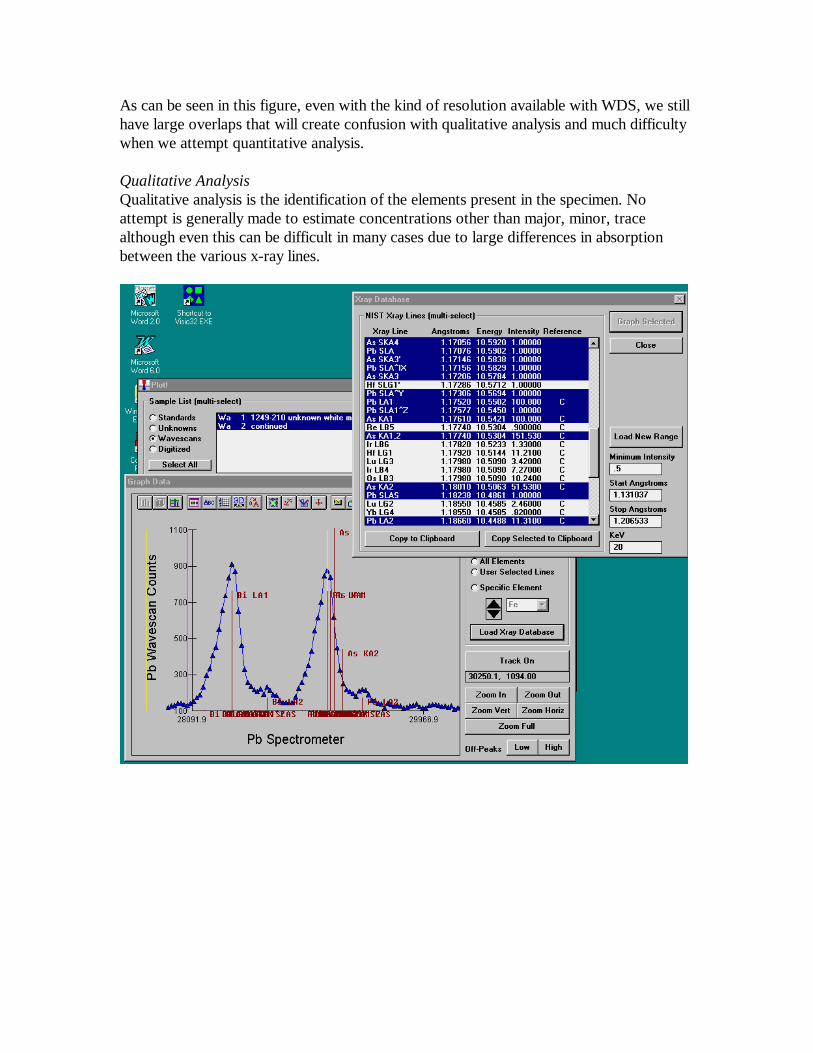
X-ray DetectionBy placing a suitable x-ray detector coupled to a set of electronic components (amplifiers,counters, analog-digital converters) and a computer, one can detect and analyze x-raysemitted from a sample undergoing electron bombardment. The resulting x-ray spectrumcan be displayed according to energy (Energy Dispersive X-ray Spectroscopy - EDS) orwavelength (Wavelength Dispersive X-ray Spectroscopy -WDS). These data can then beeither analyzed to give an indication of which elements occur in a sample (qualitative), orin a much more rigorous process, a precise and accurate (quantitative) chemical analysis.
Energy Dispersive X-ray Analysis (EDS)X-rays emitted from a sample under electron bombardment are collected with a liquidnitrogen-cooled solid state detector
EDS schematic
from J. I. Goldstein, D. E. Newbury, P. Echlin, D. C. Joy, C. Fiori, E. Lifshin, "Scanning Electron Microscopy and X-Ray Microanalysis",2nd Ed., Plenum, New York, 1992
and analyzed via computer according to their energy. Typically, the computer programsused in EDS will display a real time histogram
EDS spectra
of number of X-rays detected per channel (variable, but usually 10 electron volts/channel)versus energy expressed in keV (thousand electron volts).
In practice, EDS is most often used for qualitative elemental analysis, simply to determinewhich elements are present and their relative abundance. Depending upon the specificinvestigation's needs, researchers in need of quantitative results may be advised to use theelectron microprobe. In some instances, however, the area of interest is simply too smalland must be analyzed by TEM (where EDS is the only option) or high resolution SEM(where the low beam currents used preclude WDS, making EDS the only option).
EDS ArtifactsSystem peak, escape peaks and sum peaks, are all phenomena that an EDS user must beaware of. Modern analytical software used in processing energy dispersive x-ray spectracan generally take them into account -- but such software is not perfect. Also, many userswill look at the raw spectra, where the software may or may not have labeled the artifacts.
Peak overlaps - the spectral resolution of EDS is not a great as WDS. Resolution isusually defined as the FWHM (full width at half maximum) of pure Mn Ka: ~ 150 eV.Therefore, the separation of some peaks can be poor. Examples include the case wheresmall amounts of Fe are being investigated in the presence of large amounts of Mn (MnKb is very close to Fe Ka), and the case where Cu, Zn and Na are present together: the Llines of Cu and Zn are close to the K lines of Na.
This figure shows the problem of attempting to analyze a Ti-V alloy with a trace amountof Cr. Because of the ubiquitous k-beta overlaps in this region of the periodic table, wehave a cascade overlaps situation of a major concentration of Ti interfering with minoramount of V, which in turn significantly interferes with a trace concentration of Cr. This isa situation that definitely requires special handling to obtain quantitative results, theoverlap on the trace concentration is approximately 1000%. However, much more simpleand commonly encountered cases of minor spectral overlap often occur and the analyst isrequired to be aware of these difficulties.
One classic case was a paper published where Al was reported in the brains of patientswith Alzheimer’s disease, but was eventually shown to be caused by the mis-identificationof a minor spectral line from osmium (in osmium tetraoxide used to prepare the sample) asthe Al ka line.
Wavelength Dispersive Spectrometry (WDS)WDS was the original electron microprobe spectroscopy technique developed to measureprecisely x-ray intensities and hence accurately determine chemical compositions ofmicrovolumes (a few cubic microns) of "thick" specimens, and the instrument used is theelectron microprobe. In the 1960-70s there were roughly half a dozen companiescommercially producing them; today, there are only two (JEOL and CAMECA). A full-package An electron microprobe today costs $500-$750,000.
The key feature of the electron microprobe is a crystal-focusing spectrometer, of whichthere are usually 3-5, although one manufacturer in 1970-80 produced a 9 spectrometerinstrument that are still much in use.
WDS Schematic
from J. I. Goldstein, D. E. Newbury, P. Echlin, D. C. Joy, C. Fiori, E. Lifshin, "Scanning Electron Microscopy and X-Ray Microanalysis",2nd Ed., Plenum, New York, 1992
WDS focal circle figure
from J. I. Goldstein, D. E. Newbury, P. Echlin, D. C. Joy, C. Fiori, E. Lifshin, "Scanning Electron Microscopy and X-Ray Microanalysis",2nd Ed., Plenum, New York, 1992
X-rays (as well as many other excited particles and radiations) are produced in the"interaction volume" immediately below the impact zone of the finely focused electronbeam. A very small fraction of all x-rays will be emitted at the proper "take-off" angle toenter the WDS spectrometer acceptance angle (a much smaller fraction compared to anEDS detector mounted a few cms from the sample). Remember each element'scharacteristic x-ray has a distinct wavelength, and by adjusting the tilt of the crystal in thespectrometer, at a specific angle it will diffract the wavelength of specific element's x-rays,according to Bragg’s Law:
n dλ θ= 2 sin
Those diffracted x-rays are then directed into a gas-filled proportional counting tube,which has a thin wire (usually tungsten) running down its middle, at 1-2 kV potential. Thex-rays are absorbed by gas molecules (e.g., P10: 90% Ar, 10% CH4) in the tube, withphotoelectrons ejected; these produce a secondary cascade of interactions, yielding anamplification of the signal (approx. 106) so that it can be further amplified by the countingelectronics.
The voltage pulse produced by the incoming x-ray is accompanied by a large number (infact an infinite number with an amplitude of zero volts) of randomly generated noisepulses of a much lower voltage. These noise pulses must be rejected before the signal ispulse counted and this is the role of pulse height analysis (PHA). Simply, special electroniccircuits are adjusted so that only pulses with a certain range of energies or pulse heights(greater than the “baseline” and less than the “window”) are allowed to enter the scalerelectronics for counting.
Different diffracting crystals, with 2d (lattice spacings) varying from 2.5 to 200 Å, areused to be able diffract various ranges of wavelengths that may correspond to the primaryemission lines of various elements. In recent years, the development of 'layered syntheticcrystals" of large 2d has lead to the ability to analyze the lower Z elements (Be, B, C, N,O), although inherent limitations in the physics of the process (e.g., large loss of signal byabsorption in the sample) limit the applications.
Here is a graph which illustrates the typical range of applicability for the various crystalsfound in many electron microprobes:
Typical ranges for various analyzing crystals:
0 1 10 100Angstroms
0
20
40
60
80
Cry
stal
2D
WSi60
LiF220LiF200
PETADP
TAP
NiCrBN
Analyzing Crystals Used in EPMA (UCB SX-51)
Comparison of EDS to WDSEDS can also be used to get quantitative chemical information in many situations, and thefollowing is a comparison made at equal and optimized conditions for each method:
Comparison of EDS to WDS, Equal Beam Current (from Goldstein, et. al. 1988), pure Si and Fe,10-11 A (0.01 nA), 25 keV
60 sec P (cps/10-8 A) P/B CDL(ppm)
Si Kα EDS 5400 97 580WDS 40 1513 1,710
Fe Kα EDS 3000 57 1,000WDS 12 614 4,900
Comparison of EDS to WDS, Optimized Conditions (from Goldstein, et. al. 1988), 15 keV, 180seconds counting time:
EDS : 2 x 10⁻⁹ A (2 nA) to give 2K cps spectrum to avoid sum peaksWDS : 3 x 10 -8 A (30 nA) to give 13K cps on Si spectrometer (> 1 % dt)
Here are some cases where WDS is the preferred technique, if available:
• where greater precision is required (WDS can handle significantly higher count rates) • where the peaks are too close in EDS to be resolved (typically EDS resolution is ~150
eV, versus WDS which is ~5 eV • where trace element levels are desired, WDS has a higher P/B, yielding lower
minimum detection limits.
WDS does not usually suffer from pulse pileup (too many counts coming in, i.e. frommajor elements) that occurs in EDS, and which must be compensated for mathematically.
WDS has different spectral artifacts, compared with EDS: for WDS, one unique problemthat may occur is if a higher order reflection (n>1) of a line falls near the line of interestand this will be discussed in the section on spectral interference below.
Background correctionThe background correction in EPMA is required because of the production of continuumradiation from inelastic collisions by the incident electrons in the specimen. This radiationis the primary source of background in EPMA and is the limiting factor for minimumdetection limits for the technique.
Continuum production figure
from J. I. Goldstein, D. E. Newbury, P. Echlin, D. C. Joy, C. Fiori, E. Lifshin, "Scanning Electron Microscopy and X-Ray Microanalysis",2nd Ed., Plenum, New York, 1992
Two methods are used for background correction, the most common method is the socalled “off-peak” method which measures the background due to the continuum on eitherside of the characteristic peak. There is also an alternative method for the correction ofbackground based on the fact that the intensity of the continuum (Ic) is a function of the
mean atomic number ( Z ) of the sample.
Assuming that the off peak offsets are appropriate and no other peaks interferewith the measurement, the intensities may be linearly interpolated and subtracted from thepeak intensity. In certain cases it may be desired to utilize a measurement only on one sideof the peak or to average the off-peak measurements, however since the continuum isusually sloped and the background offsets may not be symmetrical about the characteristicpeak, care must be taken with such procedures.
An example of the necessity of carefully selecting off-peak background positions(BiPb sulfide):
Bi W
aves
can
Cou
nts
Bi Angstroms
0
500
1000
1500
5.0 5.3 Pb M4-O2 S SKBX
S KB1 S KB3 Pb SMB3 S SKB1X Pb SMB2 Pb SMB1
Pb MB
Bi SMA^4 Bi SMA^3 Bi SMA^2 Bi SMA^1
Bi MA1 Bi MA2
An example of a curved background (MgO):
O W
aves
can
Cou
nts
O Spectrometer
0.0
634.1
20000 60000
Peak interferencesAs mentioned earlier, one unique WDS spectral artifact are the higher order lines impliedby Bragg’s law in which a higher energy line can diffract at the same wavelength.However, WDS can in many cases eliminate that higher order line, by fine tuning theproportional counter electronics, applying "pulse height analysis" to energy filter out theunwanted x-rays since the higher order lines, although of similar wavelength are muchhigher in energy. In the case of some primary (n=1) overlapping lines, even for WDS,
correction for spectral interference may be required, e.g. for V Ka in the presence ofabundant Ti (Kb interference) or for B Ka in the presence of abundant Mo (M-lineinterference).
Here is an EDS spectra, of an unknown ore mineral, again acquired with a pulseprocessing time configured for maximum energy resolution.
Ore mineral (EDS)
Not a very pretty picture, since we cannot separate the Pb Lα and As Kα peaks or the PbMα and S kα peaks. From a qualitative viewpoint we can only state that it is at leastevident that that As is present from the appearance of the As Lα line and Pb likely presentfrom the appearance of the secondary L lines, although S is interfered strongly by the PbMα line and can only be inferred by the mineralogy.
Here now we have the same ore mineral sample, and it's spectra acquired in the vicinity ofthe Pb Lα and As Kα lines, using a WD spectrometer equipped with an LiF analyzingcrystal with an approximate energy equivalent resolution of 10 eV.
Ore mineral (WDS)
Pb
Wav
esca
n C
ount
s
Pb Angstroms
0
1000
2000
3000
4000
5000
1.1 1.2
Pb LA1
As KA1,2
As KA2
Pb LA2
As can be seen in this figure, even with the kind of resolution available with WDS, we stillhave large overlaps that will create confusion with qualitative analysis and much difficultywhen we attempt quantitative analysis.
Qualitative AnalysisQualitative analysis is the identification of the elements present in the specimen. Noattempt is generally made to estimate concentrations other than major, minor, tracealthough even this can be difficult in many cases due to large differences in absorptionbetween the various x-ray lines.
Quantitative analyses (Theoretical Basis)The first attempt to quantify the production of x-rays in materials was made in 1951 byRaymond Castaing, as his Ph.D. thesis at the University of Paris. Castaing proposed first,utilizing a standard along with the unknown specimen, for purpose of determining theratio of x-ray intensities in order to eliminate calibrations pertaining to spectrometerefficiency, and second, that the ratio of those intensities could be scaled to elemental massfraction within the specimen, seen here:
cc
II
iu
is
iu
is= (1)
Now let’s consider, for a moment, atomic fraction averaging as a basis for modelingelectron-solid interactions, which at first might seem more reasonable, although, it isevident to everyone that has worked in this area, that simple atomic fraction utterly fails toaccurately describe the proportion of x-ray production contributed by the various atoms ina compound. Why is this?
Figure 4
In this figure, adapted from Reed (1993), we schematically depict the penetration effect ofthe incident electron beam for a binary compound, where we have a low Z element here, ahigh Z element here, and in the center, a compound consisting of equal numbers of low Zand high Z atoms. It is evident, by simply comparing the number of colored circles withinthe interaction volumes, that the compound will contain almost as many atoms of the highZ element, as it’s pure element, but only a small fraction of the low Z element, comparedto it’s pure element.
Because of this disproportionality, Reed postulated that the electron beam penetrates aninteraction volume of constant mass for compounds of different composition. In fact, thisis only approximately true because the proportion of atomic weight (i.e., mass) to atomicnumber (electron interactions) or A/Z, is approximately a constant, because from isotopestudies, it is known that the neutron has no effect on electron solid interactions at theseenergies.
In any case, a significant complication arises because we are dealing with a "thick"specimen (more than a few microns thick): absorption of X-rays, particularly longwavelength, lower energy ones, can be an important factor in reducing the number ofcertain X-rays counted, compared to those generated in the sample.
In addition to this absorption correction (A), corrections need also be made forfluorescence (F: the generated X-rays may also produce additional X-rays of other lines inthe sample) and for 'atomic number effects'(Z). These three corrections are the matrixcorrection, ZAF, based upon various physical models developed to describe these effects,seen here:
k c Z A Fi i i i i= (2)
Traditionally, analysts have utilized mass fraction for proportioning these inter-elementeffects, although as already noted above, mass is not directly involved.
In the past, analysts have attempted to improve the accuracy of their analyses by selectingstandards that are similar in composition to the unknowns, so that there are no largeextrapolations. However, do to improvements in the algorithms used for calculation ofmatrix effects, the use of poorly characterized standards now produce the largest errors.To avoid that, we often utilize, whenever possible, pure element or simple oxide standards(MgO, Al2O3, SiO2, TiO2, etc.) that have a known stoichiometric composition.
Standards of this type may not always be possible to obtain (e.g., Na2O, K2O), and inthose cases, and for the purposes of using secondary standards as a check on the quality ofthe analyses, we can utilize standards whose compositions have been determined byclassical wet-chemistry or other gravimetric techniques, and that similar in composition tothe unknown.
Absorption CorrectionAbsorption is often the largest correction made to the x-ray intensities in quantitativemicroanalysis and therefore the accuracy with which we calculate the correction mostdirectly influences the accuracy of the quantitative results that we may obtain. Theabsorption is defined as the absorption of an x-ray by the atoms present in the sample
Traditionally absorption is considered a one of the terms in the ZAF correction, but withinthe last few decades much work has been done to describe the absorption correction as afunction of the depth distribution of the generated x-rays within the sample. Thereforeboth factors for x-ray absorption and electron scattering (electron and energy loss) areconsidered at the same time. This is called the φρz curve method.
In either case, the most important parameters for the correction are
1. incident electron energy2. x-ray takeoff angle
3. mass absorption coefficients
Th incident energy of the electron beam can be determined by careful measurements of thecontinuum in the region where the overvoltage approaches zero also known as the Duane-Hunt limit. Use of this technique can determine the true accelerating voltage to within 50volts or so.
The x-ray take-off angle can not be directly measured except by comparison of k-ratios foropposite pairs of spectrometers.
Mass absorption values which describe the photo-absorption of x-rays in the variouselements have been the subject of intense experimental effort, especially for those x-rayenergies equal to the emission line energies.
Heinrich (CITZAF) Henke (1982)Mg Kα in Si 802 859Mg Kα in Fe 6121 5250Si Kα in Mg 2825 2902Si Kα in Fe 2502 2305
As one can see there is about 20% difference in the mass absorption coefficients for Mgkα in Fe although the others are reasonably close. This difference will have a significanteffect on the quantitative analysis (about 1 % or so) in this case.
Atomic Number CorrectionThe atomic number correction is used to describe electron scattering in specimens ofvarious composition. The two primary mechanisms creating the atomic number effect arechanges in trajectory due to high angle scattering that cause little or no reduction in theenergy of the electron (elastic scattering) and can result in a significant loss of electronsbackscattered out of the sample and hence no longer involved in the production ofcharacteristic x-rays and reduction in energy of the incident electrons involved in variouselastic processes such as continuum and characteristic x-ray production as well as phonon,auger, and secondary electron production.
This correction may be calculated separately or combined in the φρz curve method alongwith the absorption correction.
Fluorescence CorrectionThe fluorescence correction is required due to the fact that not only can electrons cause x-ray fluorescence but x-rays generated by the electron beam (primary) can also causeadditional x-ray fluorescence (secondary) in other elements that may also be present.
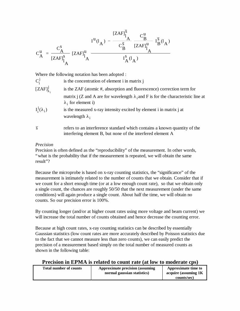
The complete form of the correction (along with an analogous correction for spectralinterference) is shown here:
CAu CA
s
[ZAF]lA
s [ZAF]lA
u
Iu (lA )
[ZAF]lA
s
CBs
CBu
[ZAF]lAu IB
s (lA )
IAs (lA )
=
−
Where the following notation has been adopted :Ci
j is the concentration of element i in matrix j
[ ]ZAFi
jλ is the ZAF (atomic #, absorption and fluorescence) correction term for
matrix j (Z and A are for wavelength λi and F is for the characteristic line atλi for element i)
Iij
i( )λ is the measured x-ray intensity excited by element i in matrix j atwavelength λi
s refers to an interference standard which contains a known quantity of theinterfering element B, but none of the interfered element A
PrecisionPrecision is often defined as the “reproducibility” of the measurement. In other words,“what is the probability that if the measurement is repeated, we will obtain the sameresult”?
Because the microprobe is based on x-ray counting statistics, the “significance” of themeasurement is intimately related to the number of counts that we obtain. Consider that ifwe count for a short enough time (or at a low enough count rate), so that we obtain onlya single count, the chances are roughly 50/50 that the next measurement (under the sameconditions) will again produce a single count. About half the time, we will obtain nocounts. So our precision error is 100%.
By counting longer (and/or at higher count rates using more voltage and beam current) wewill increase the total number of counts obtained and hence decrease the counting error.
Because at high count rates, x-ray counting statistics can be described by essentiallyGaussian statistics (low count rates are more accurately described by Poisson statistics dueto the fact that we cannot measure less than zero counts), we can easily predict theprecision of a measurement based simply on the total number of measured counts asshown in the following table:
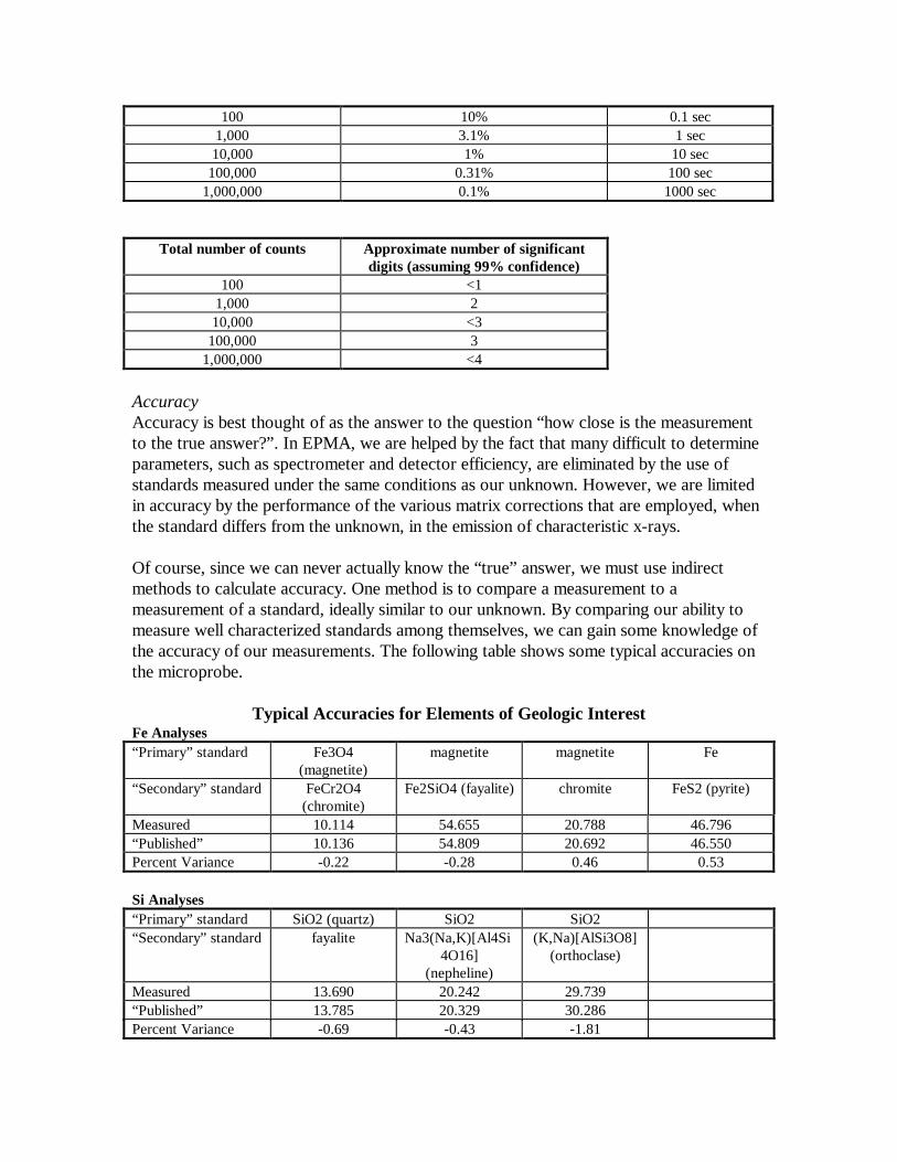
Precision in EPMA is related to count rate (at low to moderate cps)Total number of counts Approximate precision (assuming
normal gaussian statistics)Approximate time toacquire (assuming 1K
counts/sec)
100 10% 0.1 sec1,000 3.1% 1 sec10,000 1% 10 sec
100,000 0.31% 100 sec1,000,000 0.1% 1000 sec
Total number of counts Approximate number of significantdigits (assuming 99% confidence)
100 <11,000 210,000 <3
100,000 31,000,000 <4
AccuracyAccuracy is best thought of as the answer to the question “how close is the measurementto the true answer?”. In EPMA, we are helped by the fact that many difficult to determineparameters, such as spectrometer and detector efficiency, are eliminated by the use ofstandards measured under the same conditions as our unknown. However, we are limitedin accuracy by the performance of the various matrix corrections that are employed, whenthe standard differs from the unknown, in the emission of characteristic x-rays.
Of course, since we can never actually know the “true” answer, we must use indirectmethods to calculate accuracy. One method is to compare a measurement to ameasurement of a standard, ideally similar to our unknown. By comparing our ability tomeasure well characterized standards among themselves, we can gain some knowledge ofthe accuracy of our measurements. The following table shows some typical accuracies onthe microprobe.
Typical Accuracies for Elements of Geologic InterestFe Analyses“Primary” standard Fe3O4
Mg Analyses“Primary” standard MgO MgO“Secondary” standard chromite diopsideMeasured 9.229 11.311“Published” 9.166 11.192Percent Variance 0.69 1.06
Al Analyses“Secondary” standard nepheline orthoclase chromite“Primary” standard Al2O3 Al2O3 Al2O3Measured 17.607 8.379 5.181“Published” 17.868 8.849 5.250Percent Variance -1.46 -5.31 -1.32
In practice, there are two ways to proceed. The first method is that by using standards asclose as possible in composition to the unknown, and by assuming that the standardcompositions are accurately known, because the matrix correction for an unknown that isidentical in composition to the standard is exactly 1.000, we can eliminate errors due tothe matrix correction itself. However, it is not always possible to find standards withsimilar compositions to our unknowns.
The problem with this assumption is that the accuracy of the standard composition itself isnot always known. While it is easy to believe that pure Si is 99.999% Si (if we can detectno trace elements) and even pure SiO2, may be said to be 99.999% SiO2, if similar inpurity, it is quite a different thing to know the composition of a more complex compoundthat is not restricted by purity or stoichiometry (which is normally the case for a standardclose in composition to our unknown).
For example, an olivine standard requires that Mg, Fe and Si be known (assuming thatoxygen may be calculated by stoichiometry). But because there is a solid solution frompure Fe2SiO4 to Mg2SiO4, we cannot by simple stoichiometry “know” the truecomposition of the olivine standard. In an attempt to determine the “true” composition ofFe and Mg, it is required that these be measured independently of the microprobe. Onecommon method is so called “classical” wet chemical methods based on gravimetric(weighing) measurements.
This means that our wet chemical precision is related to the reproducibility of ourweighing, mixing and diluting and the accuracy is related to the accuracy of the scale. Infact wet chemical methods have their own systematic errors that affect the accuracy of thedetermination of the standard composition. For example, when Al is precipitated out ofsolution in preparation for weighing, significant Fe may also be precipitated. It is unlikelythat these systematic errors in wet chemistry would cancel any systematic errors inherentin EPMA methods.
The other way to proceed with our measurements, is to utilize pure elements or simpleoxides and assume that due to purity and constraints of stoichiometry (for simple oxides),that the compositions are accurately known. We then rely solely on the accuracy of thematrix corrections themselves. The accuracy of the matrix correction may be determinedby careful comparison of well characterized “secondary” standards. Once again, we needto judge the accuracy of these secondary standards, but it is possible, for example, that bymeasuring Si Ka in a pure Mg2SiO4 against a pure SiO2 standard, we might be able toassign a confidence in how well we can matrix correction the effect Mg on Si Ka. Sinceboth materials can be obtained pure and may be considered stoichiometric, any error inthat measurement might be considered a measurement of the accuracy of the matrixcorrection (for that particular case at least).
Trace elementsTrace elements are those measurements where due to numerous factors, the signal level ofour measurement is similar to the measurement of the background itself.
The background in the microprobe is almost entirely due to the production of continuumx-rays from the deceleration of the primary beam electrons in the sample. This presence ofthis continuum, is the limiting factor for trace elements detection in the microprobe.
To circumvent this limitation of the electron beam, some effort has been made to developfocused x-ray beams which produce much lower x-ray backgrounds. Due to the difficultyin focusing x-ray beams this still remains expensive is usually found only in largesynchrotron beam lines.
What signifies the detection of an element? Assuming again Gaussian statistics, it isusually stated that any measurement that exceeds 3 times the standard deviation of thebackground has a 99% confidence of being “real” (that is, truly present).
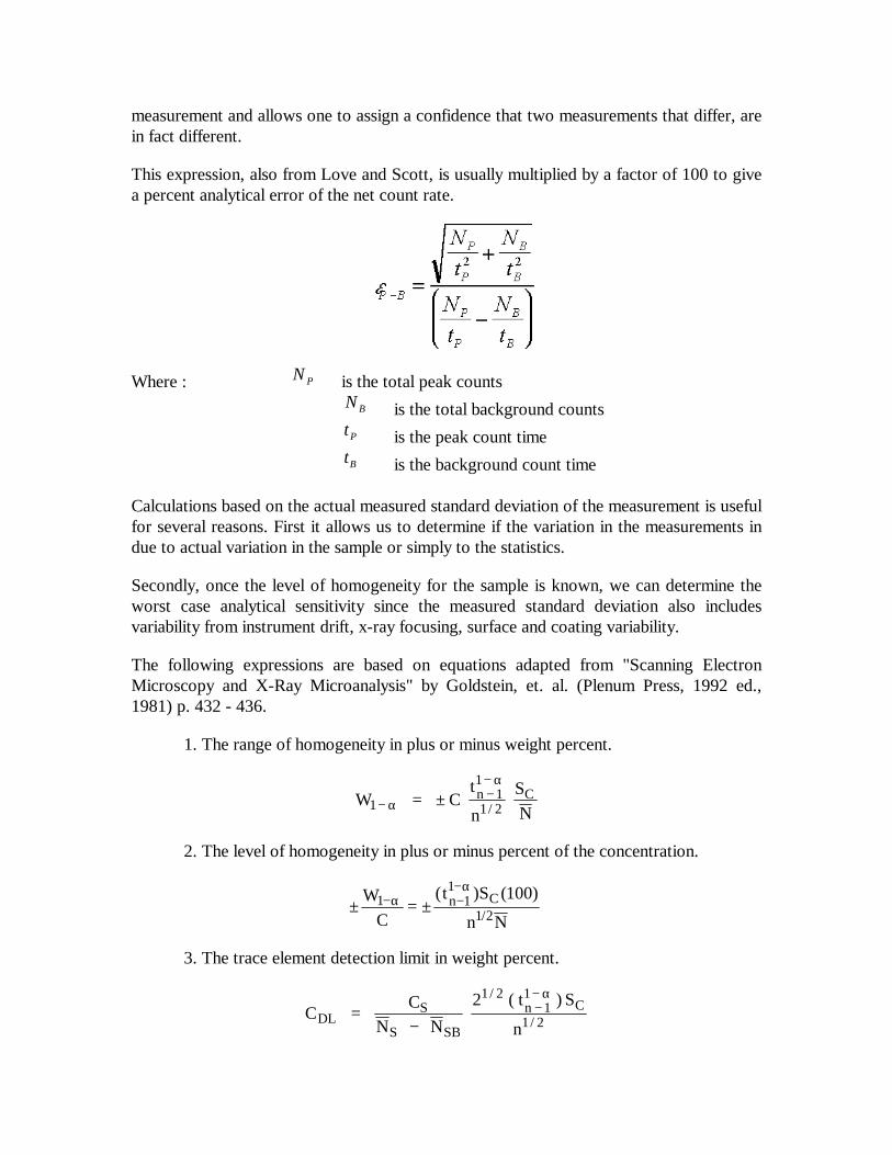
Since the standard deviation may be described as the square root of the backgroundcounts, the calculation may be performed utilizing the formula given here, adapted fromLove and Scott (1974).
CDL ZAFI
ItS
B= ⋅( )3
100
Where : ZAF is the ZAF correction factor for the sample matrixIS is the count rate on the analytical (pure element) standardIB is the background count rate on the unknown samplet is the counting time on the unknown sample
An analogous calculation which describes the analytical sensitivity of the measurement canalso be calculated from similar information. The analytical sensitivity is the precision of a
measurement and allows one to assign a confidence that two measurements that differ, arein fact different.
This expression, also from Love and Scott, is usually multiplied by a factor of 100 to givea percent analytical error of the net count rate.
Where : N P is the total peak countsN B is the total background countstP is the peak count timetB is the background count time
Calculations based on the actual measured standard deviation of the measurement is usefulfor several reasons. First it allows us to determine if the variation in the measurements indue to actual variation in the sample or simply to the statistics.
Secondly, once the level of homogeneity for the sample is known, we can determine theworst case analytical sensitivity since the measured standard deviation also includesvariability from instrument drift, x-ray focusing, surface and coating variability.
The following expressions are based on equations adapted from "Scanning ElectronMicroscopy and X-Ray Microanalysis" by Goldstein, et. al. (Plenum Press, 1992 ed.,1981) p. 432 - 436.
1. The range of homogeneity in plus or minus weight percent.
W Ct
nSN
n C1
11
1 2−−−
= ±αα
/
2. The level of homogeneity in plus or minus percent of the concentration.
± = ±− −−W
Ct S
n Nn C1 11
1 2100α
α( ) ( )/
3. The trace element detection limit in weight percent.
CC
N Nt S
nDL
S
S SB
n C=−
−−21 2
11
1 2
/
/( )α
4. The analytical sensitivity in weight percent.
∆C C CC t S
n N Nn C
B= − ′ ≥
−−−21 2
11
1 2
/
/( )
( )
α
Where : ′C is the concentration to be compared with
C is the actual concentration in weight percent of the sample
Cs is the actual concentration in weight percent of the standard
tn −−
11 α is the Student t for a 1-α confidence and n-1 degrees of freedom
n is the number of data points acquired
SC is the standard deviation of the measured values
N is the average number of counts on the unknown
NB is the continuum background counts on the unknown
NS is the average number of counts on the standard
NSB is the continuum background counts on the standard
Optimal Detection Limits on the Electron Microprobeelement (x-ray line) matrix voltage
Volatile element CorrectionSome element intensities may vary over time with exposure to the electron beam. Thismay be observed as either an increase or decrease in intensity over time. Since this effect istypically observed as a loss in intensity it is often referred to as a volatile element loss.
There are several proposed mechanisms for these effects including temperature and sub-surface charging. To see the effect that temperature could have on the specimen, here aresome calculations for beam induced heating in various samples:
∆TE ikd
= ⋅4 8 0.
Where : E0 = electron beam in KeVi = beam current in uAk = thermal conductivity in watts cm-1 K-1-1d = beam diameter in um (microns)
This is often the case for volatile elements such as sodium or potassium, but theextrapolation correction can also be applied to any degradation (or enhancement) of the x-ray intensities over time due to other causes such as sample damage, carboncontamination, etc. This correction is especially useful for samples which are too small toutilize a defocused beam and allows the user to run higher sample currents to improve theanalytical sensitivity.
For instance, when sodium loss in observed in an alkali glass sample, acorresponding gain in silicon and aluminum x-rays may be noted. The extrapolationcorrection used in Probe for Windows can be applied to some or all elements in an sample,regardless of whether the x-ray intensities are decreased or increased during theacquisition (as long as the elements to be corrected are acquired as the first elementon each spectrometer, i.e., order number = 1). The correction assumes that the changein counts is linear versus time when the natural LOG of the x-ray counts are plotted(Nielsen and Haraldur, 1981) as shown here :
Depending on the sample, this may or may not be a valid assumption. Under certainconditions, with very volatile hydrous alkali glasses, the change in count rate may actuallydecrease more quickly than a simple log decay. In this case, it may be necessary to defocusthe beam slightly before acquisition.
Sample Homogeneity on the Scale of the Beam SizeConsider the extreme situation depicted below. An interface of Al and Cu metal where theelectron beam excites x-rays from both sides of the interface.
Al Cu
e-
In this situation, x-rays of both metals will be produced. However, note that because theCu x-rays are generated mostly in a pure Cu matrix and the Al x-rays are mostly generatedin an pure Al matrix, the actual matrix correction that needs to be applied to the measuredx-rays will be different than simply the matrix correction for a homogenous alloy sampleconsisting of both Al and Cu.
Now, as you may know, the matrix correction for the x-ray of an element in the pureelement is considered to be 1.0. Hence for the majority of the x-rays produced in thissample, the matrix correction that needs to be applied to each x-ray is very close to 1.0since, as stated above, most of the Cu x-rays are generated in a pure Cu matrix and mostof the Al x-rays are generated in a pure Al matrix. However, when the microprobemeasures the x-ray intensities at this boundary and receives both Al and Cu x-rays, itknows nothing of the actual geometry, and can only assume that all the x-rays measuredare to be matrix corrected using a composition that is determined by iteratively correctingthe measured x-ray intensities. This is the nature of the ZAF or phi-rho-z matrixcorrection. Of course, one could apply a geometric model to the matrix correction to
0
5
10
15
20
25
1 2 3 4 5 6 7 8 9 10 11 12
Time in seconds
LOGcounts
Si
Na
correct for the interface effect, but this would require precise knowledge of the interfaceshape and orientation which is usually not available.
Since determining the geometry of a buried interface is difficult if not impossible,the software can only assume a matrix correction based on a composition consisting ofboth Cu and Al, since both x-rays were detected. The matrix correction for Al x-rays in ahomogenous Cu-Al alloy is of course quite different than that of pure Al, which is reallythe situation that created the Al x-rays in our example and the same is true for the Cu x-rays as well. The effect of assuming a homogenous matrix, when in fact the sample is veryinhomogenous, is to apply the wrong matrix correction to the x-rays detected from thesample.
The following is a calculation for the correction of Cu kα and Al kα x-rays in a50:50 homogenous alloy at 15kV and a 52.5 degrees takeoff angle :
As you can see, the correction for both x-rays, but especially Al kα (47% ZAFcorrection), is significantly higher than the correction for each x-ray in the pure element(1.0). This will result in a very high total as the beam straddles the interface between thetwo phases, since both x-rays will be over corrected by homogenous alloy compositionmatrix correction. This example is extreme, but the situation applies to any inhomogenoussample in which the matrix correction for the different phases present are not equal. This isbecause the matrix correction itself is non-linear and cannot be applied to the normalizedx-ray intensities generated from the different phases.
It is best to remember the words of the late Chuck Fiori, who said : "if the feature issmaller than the size of the beam, then all bets are off".
It is also important to remember that when the sample inhomogeneity is much smaller thanthe scale of the beam (for example particle phases less than 0.05 microns), that this effectbecomes insignificant due to the fact that the many phases involved in the production andabsorption of the x-rays tend to average out the contribution from a single phase. Ofcourse this also means that it is possible to only determine the average composition ofvery fine grained materials. But at least we don't have to worry about inhomogeneity onthe atomic scale!
Sample preparationPoor sample preparation- rough surfaces can preferentially bias the analysis against lowenergy x-ray as seen in this figure,Rough surface figure
Rough surface problems:
Conductive coatings (if any) must be carefully applied to clean surfaces and is required tobe of the same composition and thickness for both the standard and the unknown sample.In many cases, (light element analysis) this may require that the standards and unknownsbe coated at the same time.
Problems with sample geometryTilted sample problems:
Line of sight problems:
Incorrect sample geometry - X-rays emerge from a sample and travel line - of -sighttrajectories. Thus, if the sample is tilted incorrectly, something may actually block the pathbetween detector and sample.
This will manifest itself either as an inordinately low number of X-rays (expressed ascounts sec-1) or you may notice an absence of low energy X-rays (either due to blockingor re-absorption) in the spectrum being collected. This is not normally a concern on themicroprobe where specimens are polished flat, although it can occur when the analyzedarea is near the edge of the mounted sample as seen in the above figure.
Carbon coat thickness variation
Variations in the thickness of the carbon (or other conductor) coat, can result in adifference in intensity emitted from the specimen surface. This may result from twodifferent mechanisms.
In the first, soft x-ray emitted from the sample are absorbed by the coating, hence if theabsorption is significant enough, then differences in the thickness of the coating betweenthe standard and the unknown will produce a difference in the intensity of the x-raydetected from the sample and standards. Due to the non-linear and complex nature of theabsorption (absorption edges) it is not possible to make a general statement regarding themagnitude of the effect. The following table gives several examples for absorption ofseveral commonly measured soft x-rays in carbon coats of three different thicknesses:
Percent x-ray transmission (assume density of carbon is 2.7 gm/cm3):10 nm (carbon) 20 nm (carbon) 40 nm (carbon)
Another way in which the carbon coat can affect the emitted intensities is due to theabsorption of the primary beam electrons in the coating. This slowing down of the primaryelectrons results in an effective loss in energy of the incident electrons. For x-rays with ahigh overvoltage this reduction in primary beam energy is negligible, but for elements withan over voltage closer to 1.5 to 2 (for example Fe Ka at 10 KeV), this could affect thegenerated intensity calculation significantly.
Appendix A: Timeline of Electron Microscopy and X-ray Microanalysis
1895 - X-rays discovered by Roentgen, produced by electron bombardment of inert gas intubes; gas fluoresces and nearby photographic plates are exposed (X-rays' wavelength =0.05 - 100 Å)
1898 - Starke in Berlin found backscatter intensity varies with Z
1909 - term "characteristic x-rays" first used by Barkla and Sadler but the physical originof x-rays not clear and Kaye built an cathode ray tube with an ionization chamber to detectx-rays
1912 - Von Laue, Friedrich and Knipping confirmed that X-rays could be diffracted bycrystals with lattice spacings of similar dimension
1913 - the Bohr model of the atom explained the characteristic x-ray spectra and Braggobtained the first X-ray spectrum of Pt using an NaCl crystal (Bragg’s Law: n*lamda = 2d*sin theta )
1913 - Mosely found that there was a systematic variation of the wavelength ofcharacteristic X-rays from various elements ( wavelength inversely proportional to Zsquared )
λ = −B
Z C( )2
where B and C are constants for each characteristic line family and Z is the atomicnumber.
1922 - Hadding used X-ray spectra to chemically analyze minerals
1923 - von Hevesy discovered Hf after noticing a gap at Z=72
late 1920's - in Germany, development of transmission electron microscopes, with firstdemonstration in 1932 of transmission electron microscopy by Ernst Ruska(belated Nobel prize for it in 1986) prototype build by Siemens & Halske Co but WWIIprevented sale and use outside Germany
1930's - scanning coils added to TEM, producing STEM (image produced by secondaryelectrons emitted by specimen)
1940 - RCA sold first commercial TEM outside Germany
1942 - first use of SEM to examine surfaces of thick specimens at RCA Labs
1949 - Castaing built first electron microprobe for microchemical analysis (with crystalfocusing wavelength dispersive spectrometer = WDS) for Ph.D at Universityof Paris, and developed the basic theory
1956 - commercial production of electron microprobe began (Cameca)
1965 - commercial production of SEM began
1968 - solid state EDS detectors developed
Useful ReferencesJ. T. Armstrong, "Quantitative analysis of silicates and oxide minerals: Comparison of Monte-Carlo, ZAFand Phi-Rho-Z procedures," Microbeam Analysis--1988, p 239-246.
J. T. Armstrong, "Bence-Albee after 20 years: Review of the Accuracy of a-factor Correction Proceduresfor Oxide and Silicate Minerals," Microbeam Analysis--1988, p 469-476.
G. F. Bastin and H. J. M. Heijligers, "Quantitative Electron Probe Microanalysis of Carbon in BinaryCarbides," Parts I and II, X-Ray Spectr. 15: 135-150, 1986
J. J. Donovan, D. A. Snyder and M. L. Rivers, "An Improved Interference Correction for Trace ElementAnalysis" Microbeam Analysis, 2: 23-28, 1993
J. J. Donovan and T. N. Tingle, "An Improved Mean Atomic Number Correction for QuantitativeMicroanalysis" in Journal of Microscopy, v. 2, 1, p. 1-7, 1996
J. I. Goldstein, D. E. Newbury, P. Echlin, D. C. Joy, C. Fiori, E. Lifshin, "Scanning Electron Microscopyand X-Ray Microanalysis", Plenum, New York, 1981
J. I. Goldstein, D. E. Newbury, P. Echlin, D. C. Joy, C. Fiori, E. Lifshin, "Scanning Electron Microscopyand X-Ray Microanalysis", 2nd Ed., Plenum, New York, 1992
K. F. J. Heinrich, "Mass Absorption Coefficients for Electron Probe Microanalysis" in Proc. 11thICXOM 67: 1, 1982.
McQuire, A. V., Francis, C. A., Dyar, M. D., "Mineral standards for electron microprobe analysis ofoxygen", Am. Mineral., 77, 1992, p. 1087-1091.
Nielsen, C. H. and Sigurdsson, H., "Quantitative methods for electron microprobe analysis of sodium innatural and synthetic glasses", Am. Mineral., 66, p. 547-552, 1981
J. L. Pouchou and F. M. A. Pichoir, "Determination of Mass Absorption Coefficients for Soft X-Rays byuse of the Electron Microprobe" Microbeam Analysis, Ed. D. E. Newbury, San Francisco Press, 1988, p.319-324.
S. J. B. Reed, Electron Probe Analysis, 2nd ed., Cambridge University Press, Cambridge, 1993
V. D. Scott and G. Love, "Quantitative Electron-Probe Microanalysis", Wiley & Sons, New York, 1983
K. G. Snetsinger, T. E. Bunch and K. Keil, "Electron Microprobe Analysis of Vanadium in the Presenceof Titanium", Am. Mineral., v. 53, (1968) p. 1770-1773