Page 1
Electron Spin Resonance Study
on the Magnetic Properties of Graphene
and Its Derivative
A Thesis Submitted to the University of Manchester for the Degree of
Doctor of Philosophy in the Faculty of Science and Engineering
2019
Oka Pradipta Arjasa Putra
Department of Chemistry
University of Manchester
Page 2
P a g e | 1
Contents
Contents ................................................................................................................ 1
List of Figures and Tables ..................................................................................... 7
Figures ............................................................................................................... 7
Tables .............................................................................................................. 17
List of Abbreviations ........................................................................................... 18
Abstract ............................................................................................................... 22
Declaration .......................................................................................................... 24
Copyright Statement ........................................................................................... 25
Acknowledgements ............................................................................................. 26
1. CHAPTER ONE ......................................................................................... 27
Introduction ..................................................................................................... 27
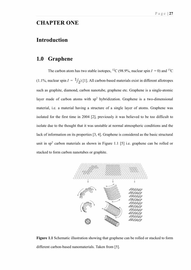
1.0 Graphene ............................................................................................. 27
1.1 Properties of graphene......................................................................... 28
1.2 Applications of graphene .................................................................... 30
1.3 Production of graphene ....................................................................... 32
1.3.1 Anodic bonding ............................................................................... 33
1.3.2 Photo exfoliation ............................................................................. 34
1.3.3 Liquid phase exfoliation .................................................................. 34
1.3.4 Electrochemical exfoliation ............................................................ 36
1.3.5 Reduced graphene oxide ................................................................. 39
1.3.6 Thermal decomposition of SiC ....................................................... 41
Page 3
P a g e | 2
1.3.7 Growth of graphene on metallic surfaces by precipitation ............. 42
1.3.8 Chemical vapour deposition ............................................................ 42
1.3.9 Molecular beam epitaxy .................................................................. 43
Analytical techniques to study graphene ........................................................ 44
1.4 Electron paramagnetic resonance spectroscopy .................................. 44
1.4.1 Electron paramagnetic resonance basic principle ........................... 44
1.4.2 State-of-the-art of EPR in graphene ................................................ 59
1.5 Raman spectroscopy ........................................................................... 67
1.5.1 Raman basic principles ................................................................... 67
1.5.2 Raman spectrum of graphene .......................................................... 69
1.6 Aims and objectives ............................................................................ 74
2. CHAPTER TWO ........................................................................................ 75
Electron Paramagnetic Resonance Study of Graphene Laminates ................. 75
2.0 Introduction ......................................................................................... 75
2.1 Sample Preparation ............................................................................. 78
2.1.1 Liquid phase exfoliation graphene laminate ................................... 78
2.1.2 Graphite ........................................................................................... 78
2.1.3 Electron paramagnetic resonance .................................................... 79
2.1.4 UV-Vis spectroscopy ....................................................................... 80
2.1.5 Atomic Force Microscope (AFM) .................................................. 80
2.1.6 Raman spectroscopy ....................................................................... 81
2.2 Results and Discussion ........................................................................ 81
Page 4
P a g e | 3
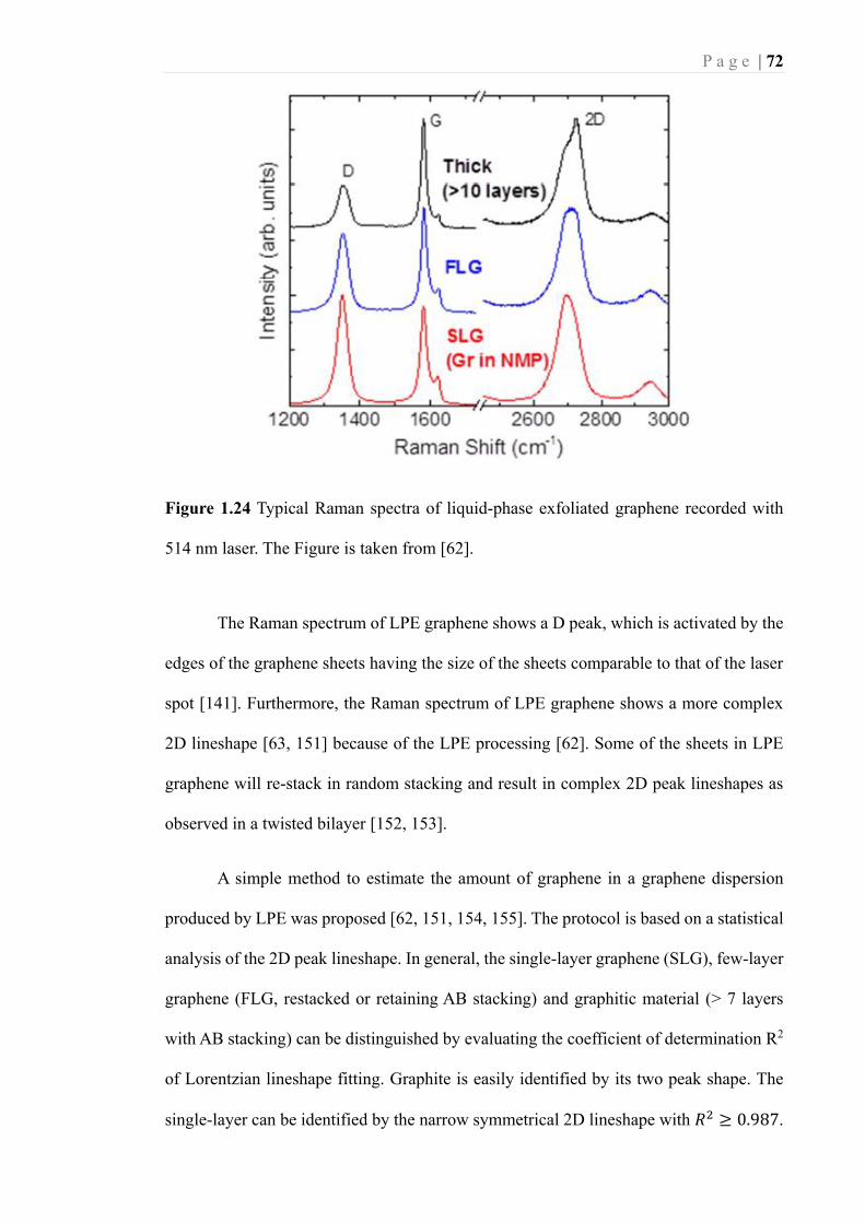
2.2.1 Graphene flake characterization ...................................................... 81
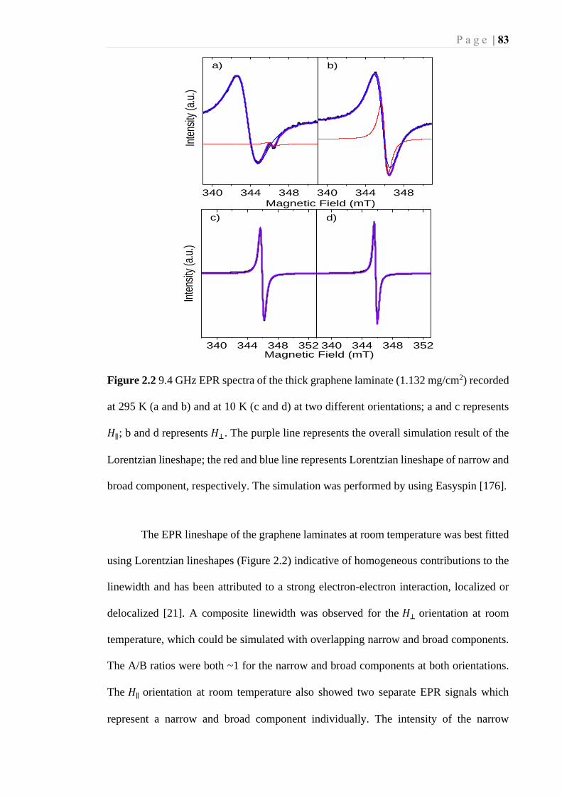
2.2.2 Graphene laminate paramagnetism ................................................. 82
2.2.3 Temperature dependence of graphene laminates ............................ 85
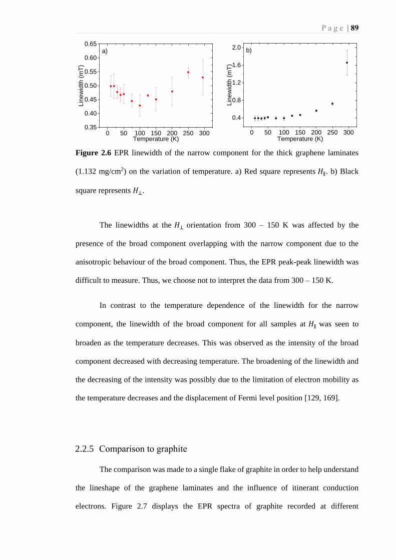
2.2.4 EPR linewidth of graphene laminates ............................................. 87
2.2.5 Comparison to graphite ................................................................... 89
2.2.6 EPR magnetic susceptibility of graphene laminates ....................... 92
2.2.7 Relaxation times and nuclear resonances of the graphene laminates
……………………………………………………………………. 96
2.3 Conclusion .......................................................................................... 97
3. CHAPTER THREE ..................................................................................... 99
Electron Paramagnetic Resonance Study of the Electrochemical Exfoliation of
Graphite in Comparison to Graphene Laminates Produced Through
Electrochemical Exfoliation, Liquid Phase Exfoliation and Chemical
Reduction of Graphene Oxide ........................................................................ 99
3.0 Introduction ......................................................................................... 99
3.1 Sample Preparation ........................................................................... 101
3.1.1 Liquid Phase Exfoliation ............................................................... 101
3.1.2 Electrochemical Exfoliation .......................................................... 101
3.1.3 Reduced Graphene Oxide ............................................................. 102
3.1.4 Electron Paramagnetic Resonance (EPR) Spectroscopy............... 102
3.1.5 Atomic Force Microscope (AFM) ................................................ 103
3.1.6 Raman Spectroscopy ..................................................................... 103
3.2 Results and Discussion ...................................................................... 104
Page 5
P a g e | 4
3.2.1 Observation of Electrochemical Exfoliated Graphite by Electron
Paramagnetic Resonance and Raman Spectroscopy .................... 104
3.2.2 Graphene flakes characterization .................................................. 109
3.2.3 Defect-induced paramagnetism ..................................................... 110
3.2.4 Temperature dependence ............................................................... 114
3.3 Conclusion ........................................................................................ 119
4. CHAPTER FOUR ..................................................................................... 121
Paramagnetic Stability and Defect Creation of Graphene Laminates Under
Controlled Conditions and Action of Laser .................................................. 121
4.0 Introduction ....................................................................................... 121
4.1 Sample Preparation ........................................................................... 123
4.1.1 Liquid phase exfoliation graphene laminate ................................. 123
4.1.2 Paramagnetic stability experiment using EPR .............................. 123
4.1.3 The aged graphene laminate experiment....................................... 123
4.1.4 In-situ defect creation experiment studied using EPR .................. 125
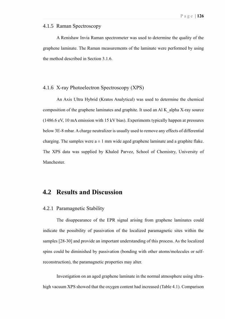
4.1.5 Raman Spectroscopy ..................................................................... 126
4.1.6 X-ray Photoelectron Spectroscopy (XPS) ..................................... 126
4.2 Results and Discussion ...................................................................... 126
4.2.1 Paramagnetic Stability .................................................................. 126
4.2.2 Defect creation on an aged graphene laminate sample ................. 133
4.2.3 In-situ defect creation by irradiation at 270 nm, 660 nm and 800 nm
…………………………………………………………………... 136
4.3 Conclusion ........................................................................................ 141
Page 6
P a g e | 5
5. CHAPTER FIVE ....................................................................................... 142
Electron Paramagnetic Resonance Study of Fluorinated Graphene Laminate
...................................................................................................................... 142
5.0 Introduction ....................................................................................... 142
5.1 Sample Preparation ........................................................................... 144
5.1.1 Liquid phase exfoliation fluorinated graphene laminate ............... 144
5.1.2 Electron Paramagnetic Resonance spectroscopy .......................... 144
5.1.3 Fourier-Transform Infrared spectroscopy ..................................... 145
5.1.4 Raman spectroscopy ..................................................................... 145
5.2 Results and Discussion ...................................................................... 146
5.2.1 Fluorinated graphene laminate ...................................................... 146
5.2.2 Paramagnetism of fluorinated graphene laminate ......................... 150
5.2.3 Temperature-dependence of the EPR resonance ........................... 151
5.2.4 HYSCORE spectroscopy .............................................................. 156
5.3 Conclusion ........................................................................................ 160
6. CHAPTER SIX ......................................................................................... 162
Conclusions and Future Work ....................................................................... 162
6.0 Conclusions ....................................................................................... 162
6.1 Future work ....................................................................................... 165
References ......................................................................................................... 167
Appendix A ....................................................................................................... 199
Appendix B ....................................................................................................... 206
Page 7
P a g e | 6
Appendix C ....................................................................................................... 207
C.1 CW EPR Code Simulation ................................................................ 207
C.2 HYSCORE Code Simulation ............................................................ 208
Word count: 43289
Page 8
P a g e | 7
List of Figures and Tables
Figures
Figure 1.1 Schematic illustration showing that graphene can be rolled or stacked to form
different carbon-based nanomaterials. Taken from [5]. .......................................... 27
Figure 1.2 Schematic showing the two types of edges in graphene, the armchair edges
and the zigzag edges. Taken from [12]. .................................................................. 28
Figure 1.3 (A) Photograph of a 50 μm aperture partially covered by mono and bilayer
graphene. The line scan profile shows the intensity of the transmitted white light
along the yellow line. The inset shows a metal support structure with different sizes
of aperture. (B) Transmittance spectrum of single-layer graphene (open circles). The
red and green line is the theoretical transmittance expected for ideal Dirac electrons
and graphene, respectively. The inset shows the transmittance of white light as a
function of the number of graphene layers. Taken from [13]. ................................ 29
Figure 1.4 Methods for producing graphene. Each of them has its own advantages and
disadvantages related to graphene size, quality and application purposes. Taken from
[55]. ......................................................................................................................... 33
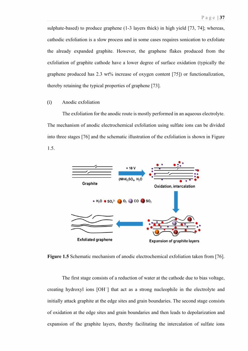
Figure 1.5 Schematic mechanism of anodic electrochemical exfoliation taken from [76].
................................................................................................................................. 37
Figure 1.6 High-resolution transmission electron microscopy (HRTEM) image of single-
layer rGO. Colour scheme highlighted different features. Light grey colour
represents the defect-free areas. Dark grey colour represents contaminated regions.
Blue colour represents disordered single-layer carbon network or extended
topological defects identified as remnants of the oxidation-reduction process. Red
Page 9
P a g e | 8
colour represents individual adatoms or substitutions. Green colour represents
isolated topological defects. Yellow colour represents holes and their edge
reconstructions. The scale bar is 1 nm. The image is taken from [96]. ................... 41
Figure 1.7 Schematic diagram of the wet-transfer process taken from [103]. ............... 43
Figure 1.8 Energy levels of an unpaired electron spin in the applied magnetic field.
Resonant energy absorption (Equation 1.3) leads to an electron spin ‘flip’ or
transition resulting in an EPR signal. The signal can be presented in absorption
(dotted) or first derivative (solid) mode. Taken from [112]. ................................... 46
Figure 1.9 Typical anisotropic axial spectra for 𝑔𝑧 > 𝑔𝑥 = 𝑔𝑦: 1st derivative line (red)
and absorption line (blue). The Figure was made using a simulator provided in
www.eprsimulator.org [114].................................................................................... 49
Figure 1.10 Typical rhombic symmetry spectra: 1st derivative line (red) and absorption
line (blue). The Figure was made using a simulator provided in
www.eprsimulator.org [114].................................................................................... 50
Figure 1.11 Energy level diagram in a fixed magnetic field for a system with S = 1 2⁄ and
I = 1 2⁄ , in the highfield approximation, showing the electron eeeman (Ee) and
nuclear eeeman (Ne) levels, and the perturbation arising from the hyperfine
interaction (HF). The two allowed EPR transitions (solid arrows) result in the
experimentally observed resonances labelled EPR I and EPR II (shown in the inset).
Adapted from [112]. ................................................................................................ 51
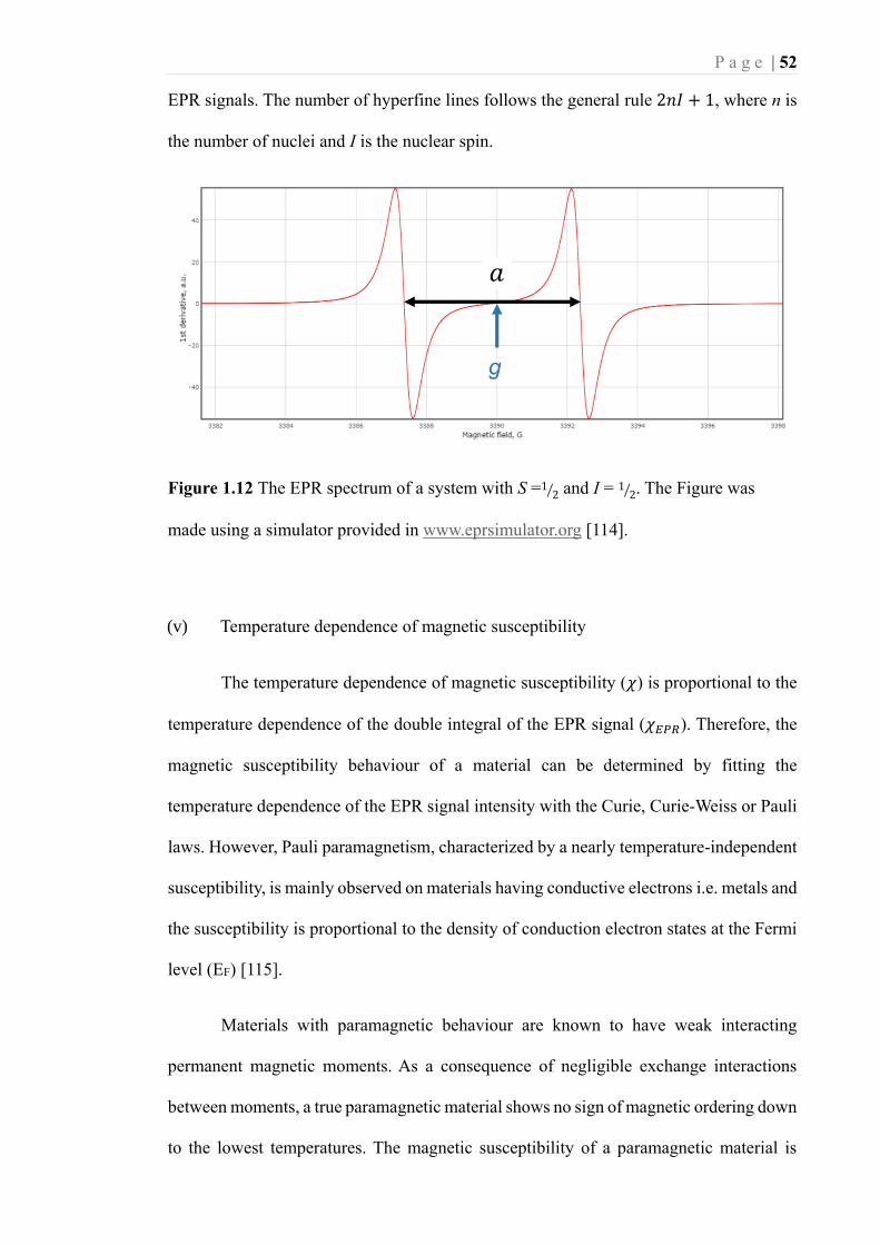
Figure 1.12 The EPR spectrum of a system with S =1 2⁄ and I = 1 2⁄ . The Figure was
made using a simulator provided in www.eprsimulator.org [114]. ......................... 52
Figure 1.13 The temperature dependence of the reciprocal magnetic susceptibility. a)
Curie law behaviour of a paramagnet; b) Curie-Weiss law behaviour of a
Page 10
P a g e | 9
ferromagnet; c) Curie-Weiss law behaviour of an antiferromagnet; d) behaviour of a
ferrimagnet. Figure a-b is taken from [116], Figure c-d is taken from [115]. ......... 54
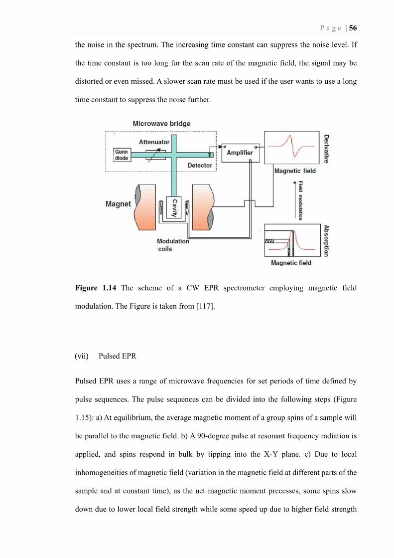
Figure 1.14 The scheme of a CW EPR spectrometer employing magnetic field
modulation. The Figure is taken from [117]. .......................................................... 56
Figure 1.15 Illustration of the magnetization vector at characteristic positions in the
typical 2-pulse sequence. Adapted from [118]. ....................................................... 57
Figure 1.16 a) 2D HYSCORE spectrum where full squares ■ represent cross-peaks from
weakly coupled nuclei in the (+,+) quadrant, and full circles ● represent cross-peaks
from strongly coupled nuclei in the (-,+) quadrant. 𝑣𝐿 is the Larmor frequency for
the nucleus of interest, A is the hyperfine coupling, 𝑣𝛼(= 𝜔12) and 𝑣𝛽(= 𝜔34); b)
(+,+) quadrant for the powder HYSCORE pattern for an S = I = 1 2⁄ spin system
with an axial hyperfine tensor. The Figure is taken from [112]. ............................. 59
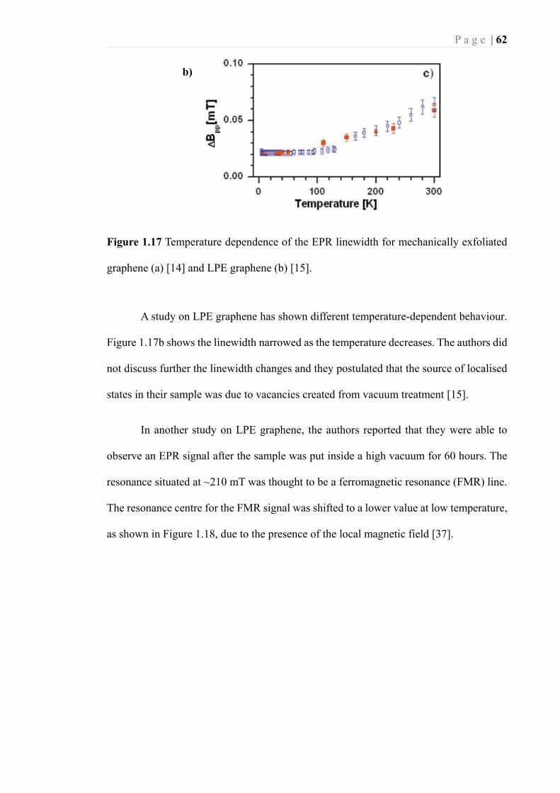
Figure 1.17 Temperature dependence of the EPR linewidth for mechanically exfoliated
graphene (a) [14] and LPE graphene (b) [15]. ........................................................ 62
Figure 1.18 a) Temperature dependence of the electron spin resonance (ESR) signal from
LPE graphene. b) Temperature dependence of normalized ESR susceptibility
measured after the annealing treatment showing a weaker signal which assigned to
the conducting electrons. The solid line corresponds to the Curie law. The spectrum
in the inset was recorded at 100 K with 64 accumulations. The Figure is taken from
[37]. ......................................................................................................................... 63
Figure 1.19 Temperature dependence of the linewidth from multilayer graphene. The
inset shows the temperature independence of the g-value. The Figure is taken from
[20]. ......................................................................................................................... 64
Page 11
P a g e | 10
Figure 1.20 EPR spectra of (a) SGN18 graphite powder, (b) ultrasounded, (c) shear mixed,
and (d) stirred few-layer graphene. The inset shows the uniaxial g-value simulated
EPR lineshape for the stirrer prepared sample. The Figure is taken from [127]..... 65
Figure 1.21 Schematic of the Rayleigh and Raman processes. The lowest energy
vibrational state m is shown at the foot with a state one vibrational unit in energy
above it labelled n. Rayleigh scattering also occurs from higher vibrational levels
such as n. Taken from [140] .................................................................................... 68
Figure 1.22 a) Mechanically exfoliated graphene showing both monolayer and bi-layer
regions. b) Raman spectra of mono and bi-layer graphene. The top and bottom insets
represent the enlarged 2D bands of regions B and A, respectively. The Figure is
taken from [143]. ..................................................................................................... 69
Figure 1.23 Raman spectrum of defective graphene showing the main Raman features
taken with a laser excitation energy of 2.41 eV. The Figure is taken from [148]. .. 71
Figure 1.24 Typical Raman spectra of liquid-phase exfoliated graphene recorded with
514 nm laser. The Figure is taken from [62]. .......................................................... 72
Figure 2.1 Graphene flake shapes (a) and size distribution (b), analyzed by using AFM.
................................................................................................................................. 82
Figure 2.2 9.4 GHz EPR spectra of the thick graphene laminate (1.132 mg/cm2) recorded
at 295 K (a and b) and at 10 K (c and d) at two different orientations; a and c
represents 𝐻∥ ; b and d represents 𝐻⊥ . The purple line represents the overall
simulation result of the Lorentzian lineshape; the red and blue line represents
Lorentzian lineshape of narrow and broad component, respectively. The simulation
was performed by using Easyspin [176]. ................................................................ 83
Page 12
P a g e | 11
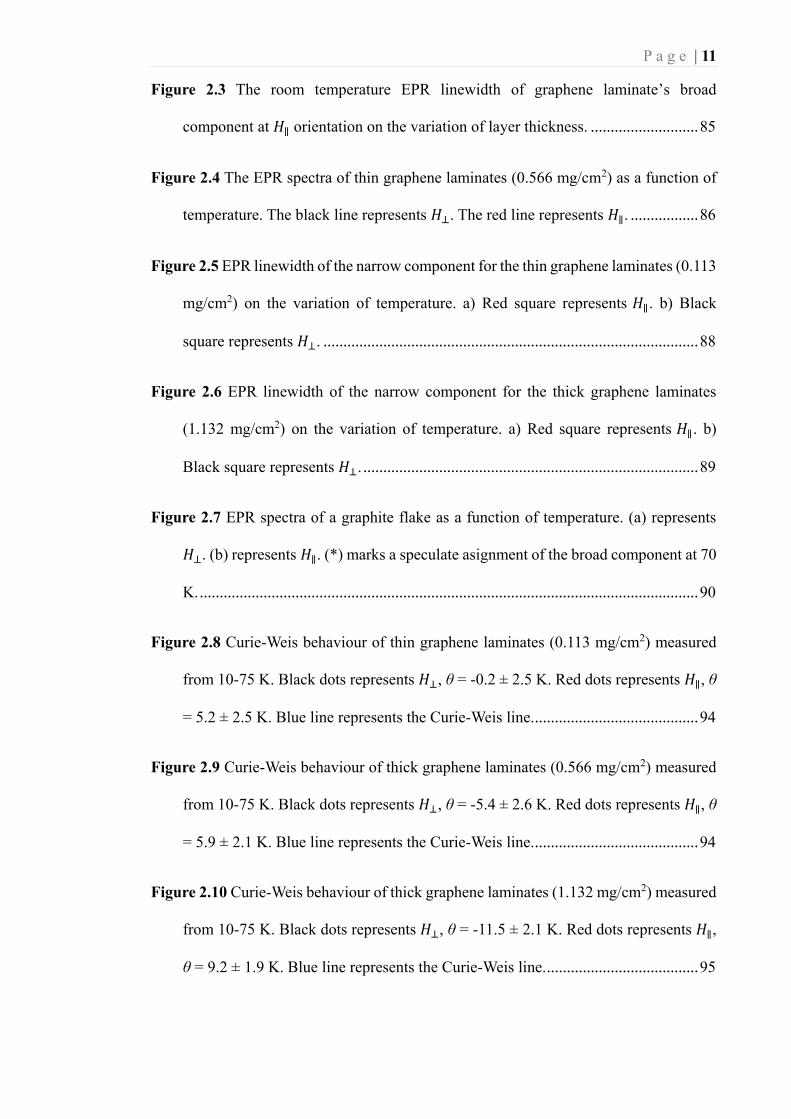
Figure 2.3 The room temperature EPR linewidth of graphene laminate’s broad
component at 𝐻∥ orientation on the variation of layer thickness. ........................... 85
Figure 2.4 The EPR spectra of thin graphene laminates (0.566 mg/cm2) as a function of
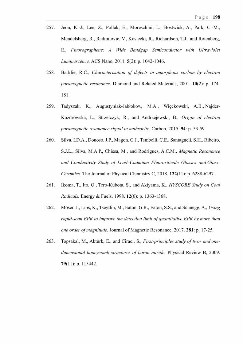
temperature. The black line represents 𝐻⊥. The red line represents 𝐻∥. ................. 86
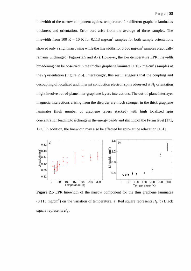
Figure 2.5 EPR linewidth of the narrow component for the thin graphene laminates (0.113
mg/cm2) on the variation of temperature. a) Red square represents 𝐻∥ . b) Black
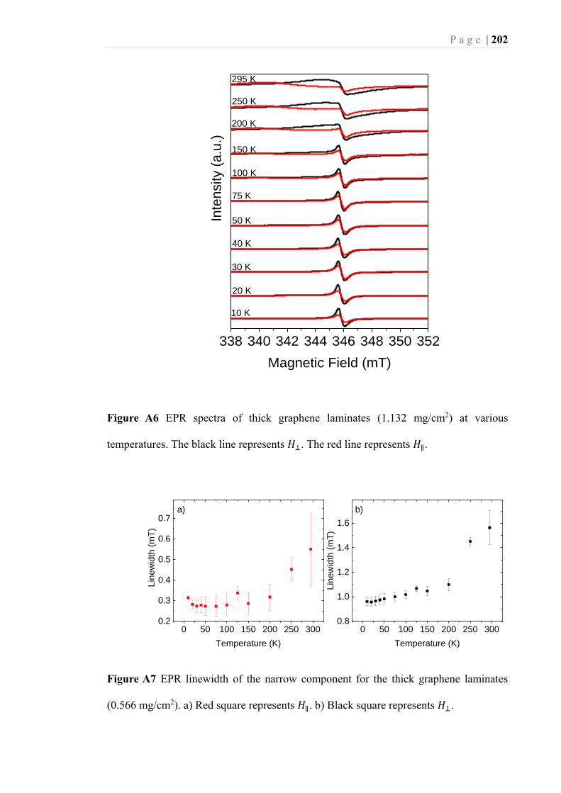
square represents 𝐻⊥. .............................................................................................. 88
Figure 2.6 EPR linewidth of the narrow component for the thick graphene laminates
(1.132 mg/cm2) on the variation of temperature. a) Red square represents 𝐻∥ . b)
Black square represents 𝐻⊥. .................................................................................... 89
Figure 2.7 EPR spectra of a graphite flake as a function of temperature. (a) represents
𝐻⊥. (b) represents 𝐻∥. (*) marks a speculate asignment of the broad component at 70
K. ............................................................................................................................. 90
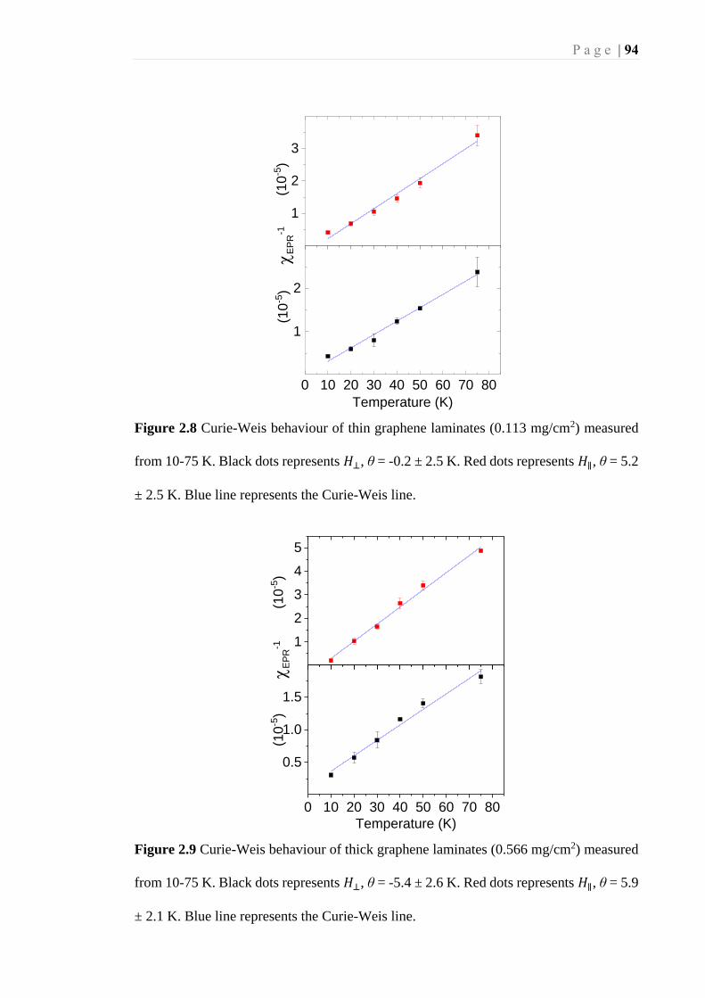
Figure 2.8 Curie-Weis behaviour of thin graphene laminates (0.113 mg/cm2) measured
from 10-75 K. Black dots represents 𝐻⊥, θ = -0.2 ± 2.5 K. Red dots represents 𝐻∥, θ
= 5.2 ± 2.5 K. Blue line represents the Curie-Weis line. ......................................... 94
Figure 2.9 Curie-Weis behaviour of thick graphene laminates (0.566 mg/cm2) measured
from 10-75 K. Black dots represents 𝐻⊥, θ = -5.4 ± 2.6 K. Red dots represents 𝐻∥, θ
= 5.9 ± 2.1 K. Blue line represents the Curie-Weis line. ......................................... 94
Figure 2.10 Curie-Weis behaviour of thick graphene laminates (1.132 mg/cm2) measured
from 10-75 K. Black dots represents 𝐻⊥, θ = -11.5 ± 2.1 K. Red dots represents 𝐻∥,
θ = 9.2 ± 1.9 K. Blue line represents the Curie-Weis line. ...................................... 95
Page 13
P a g e | 12
Figure 2.11 The spin-spin relaxation time (T2) (a) and spin-lattice relaxation time (T1) (b)
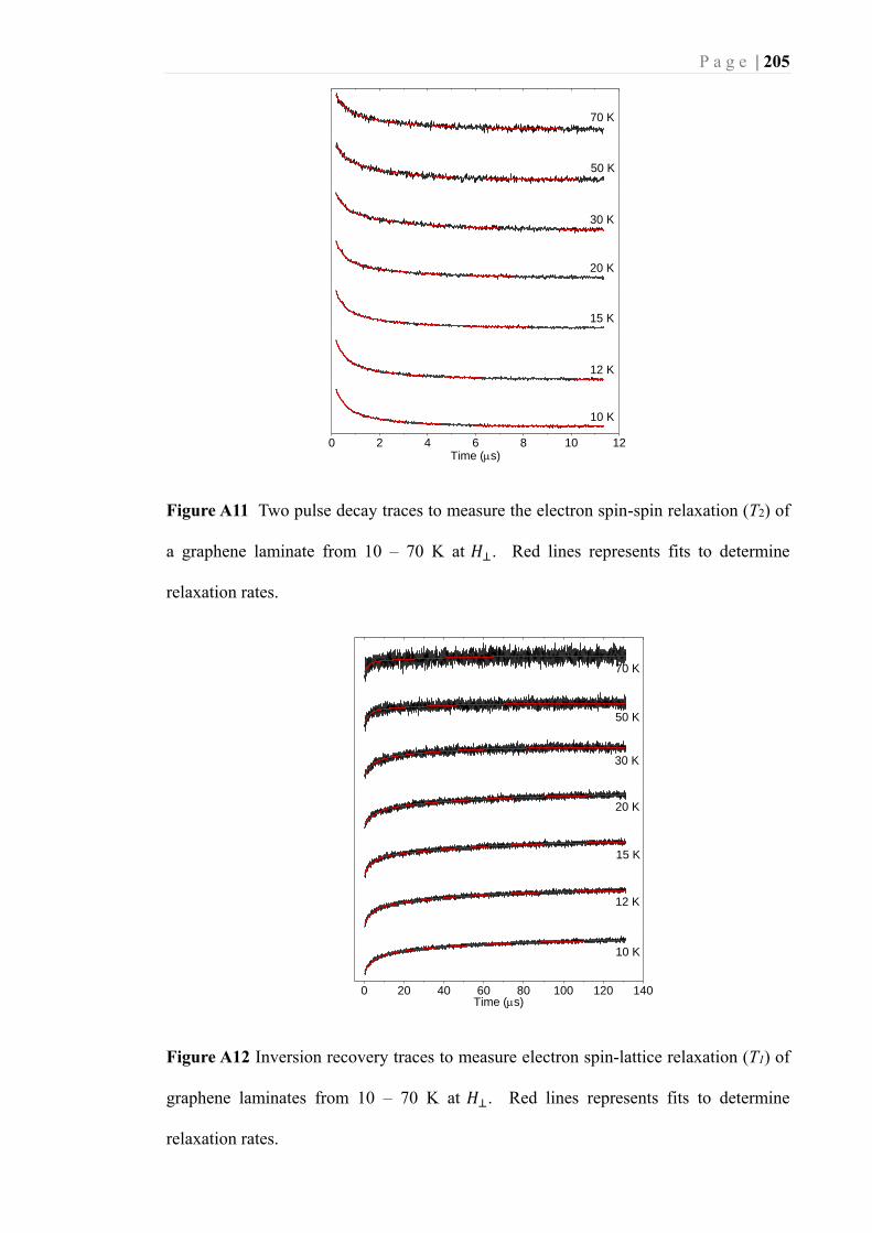
of a graphene laminate over the temperature range of 10 – 70 K at the 𝐻⊥ orientation.
................................................................................................................................. 96
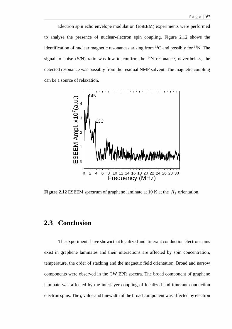
Figure 2.12 ESEEM spectrum of graphene laminate at 10 K at the 𝐻⊥ orientation. .... 97
Figure 3.1 The anode (a) and the cathode (b) after 30 seconds of the electrochemical
exfoliation process. ............................................................................................... 104
Figure 3.2 EPR spectra of the anode graphite foil before and after 30 seconds of the
electrochemical exfoliation process. The solid and dash lines represent the EPR
spectra before and after electrochemical exfoliation, respectively. The black and red
colours represent the EPR spectra at 𝐻⊥ and 𝐻∥ orientations, respectively. ......... 105
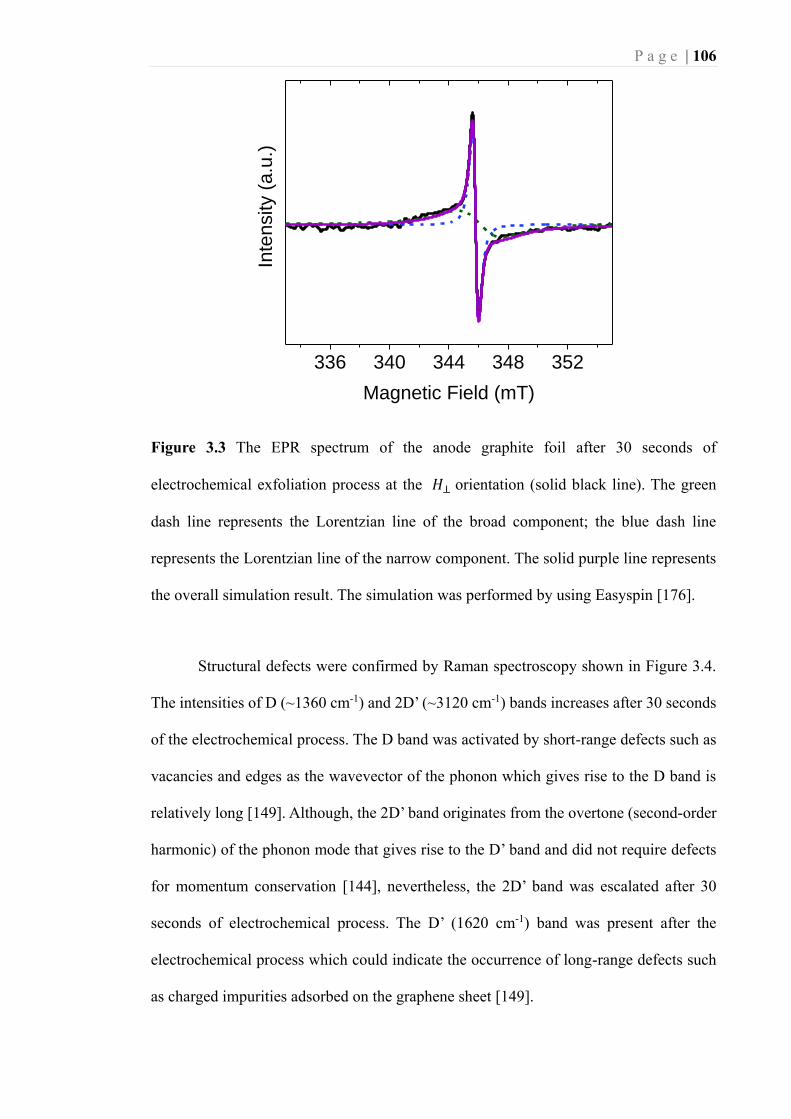
Figure 3.3 The EPR spectrum of the anode graphite foil after 30 seconds of
electrochemical exfoliation process at the 𝐻⊥ orientation (solid black line). The
green dash line represents the Lorentzian line of the broad component; the blue dash
line represents the Lorentzian line of the narrow component. The solid purple line
represents the overall simulation result. The simulation was performed by using
Easyspin [176]. ...................................................................................................... 106
Figure 3.4 Raman spectra of anode graphite foil before (black) and after (red) 30 seconds
of electrochemical exfoliation. .............................................................................. 107
Figure 3.5 EPR spectra of cathode graphite foil before and after 30 seconds of the
electrochemical exfoliation process. The solid and dash lines represent the EPR
spectra before and after electrochemical exfoliation respectively. The black and red
colours represent the EPR spectra at 𝐻⊥ and 𝐻∥ orientations, respectively. ......... 108
Figure 3.6 Raman spectra of cathode graphite foil before (black) and after 30 seconds
(red) of electrochemical exfoliation. ..................................................................... 109
Page 14
P a g e | 13
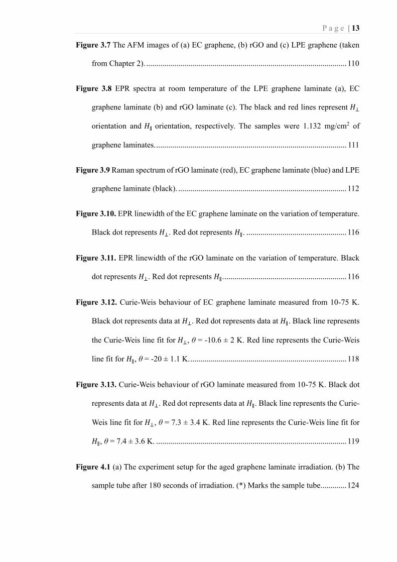
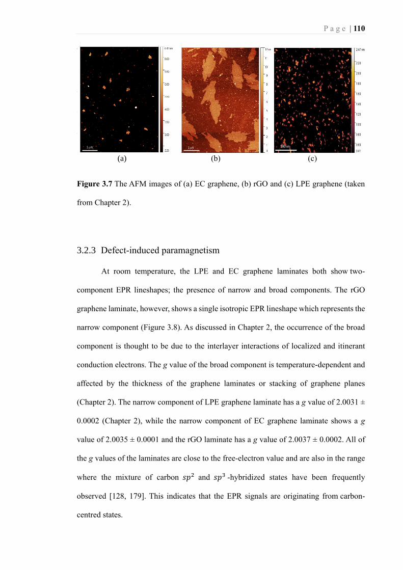
Figure 3.7 The AFM images of (a) EC graphene, (b) rGO and (c) LPE graphene (taken
from Chapter 2). .................................................................................................... 110
Figure 3.8 EPR spectra at room temperature of the LPE graphene laminate (a), EC
graphene laminate (b) and rGO laminate (c). The black and red lines represent 𝐻⊥
orientation and 𝐻∥ orientation, respectively. The samples were 1.132 mg/cm2 of
graphene laminates. ............................................................................................... 111
Figure 3.9 Raman spectrum of rGO laminate (red), EC graphene laminate (blue) and LPE
graphene laminate (black). .................................................................................... 112
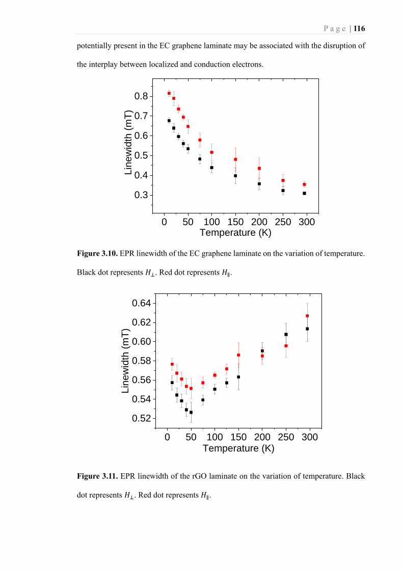
Figure 3.10. EPR linewidth of the EC graphene laminate on the variation of temperature.
Black dot represents 𝐻⊥. Red dot represents 𝐻∥. .................................................. 116
Figure 3.11. EPR linewidth of the rGO laminate on the variation of temperature. Black
dot represents 𝐻⊥. Red dot represents 𝐻∥. ............................................................. 116
Figure 3.12. Curie-Weis behaviour of EC graphene laminate measured from 10-75 K.
Black dot represents data at 𝐻⊥. Red dot represents data at 𝐻∥. Black line represents
the Curie-Weis line fit for 𝐻⊥, θ = -10.6 ± 2 K. Red line represents the Curie-Weis
line fit for 𝐻∥, θ = -20 ± 1.1 K. .............................................................................. 118
Figure 3.13. Curie-Weis behaviour of rGO laminate measured from 10-75 K. Black dot
represents data at 𝐻⊥. Red dot represents data at 𝐻∥. Black line represents the Curie-
Weis line fit for 𝐻⊥, θ = 7.3 ± 3.4 K. Red line represents the Curie-Weis line fit for
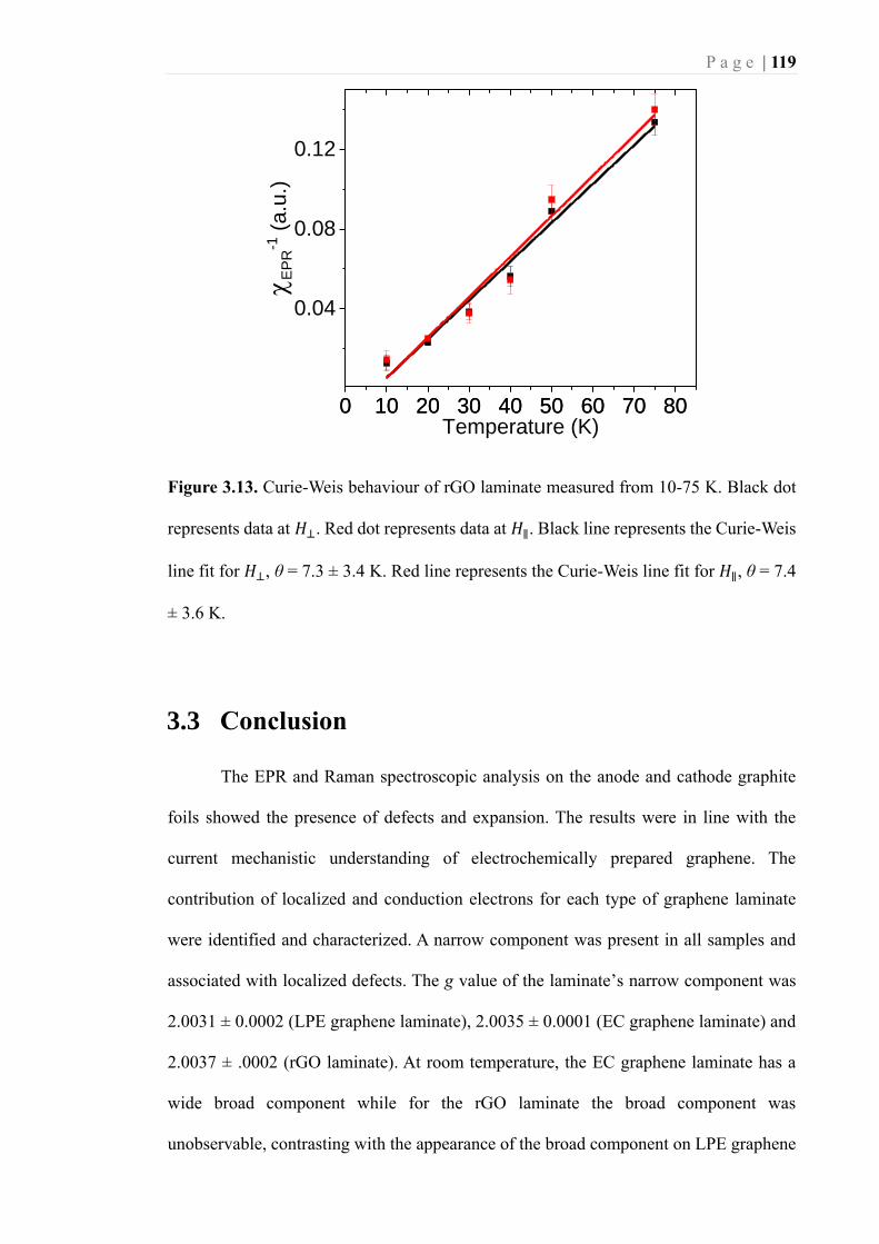
𝐻∥, θ = 7.4 ± 3.6 K. ............................................................................................... 119
Figure 4.1 (a) The experiment setup for the aged graphene laminate irradiation. (b) The
sample tube after 180 seconds of irradiation. (*) Marks the sample tube............. 124
Page 15
P a g e | 14
Figure 4.2 EPR spectrum at room temperature of an aged graphene laminate. The black
and red signals represent the 𝐻⊥ and 𝐻∥ orientations, respectively. The blue line
represents the EPR background from the EPR tube and cavity. ........................... 128
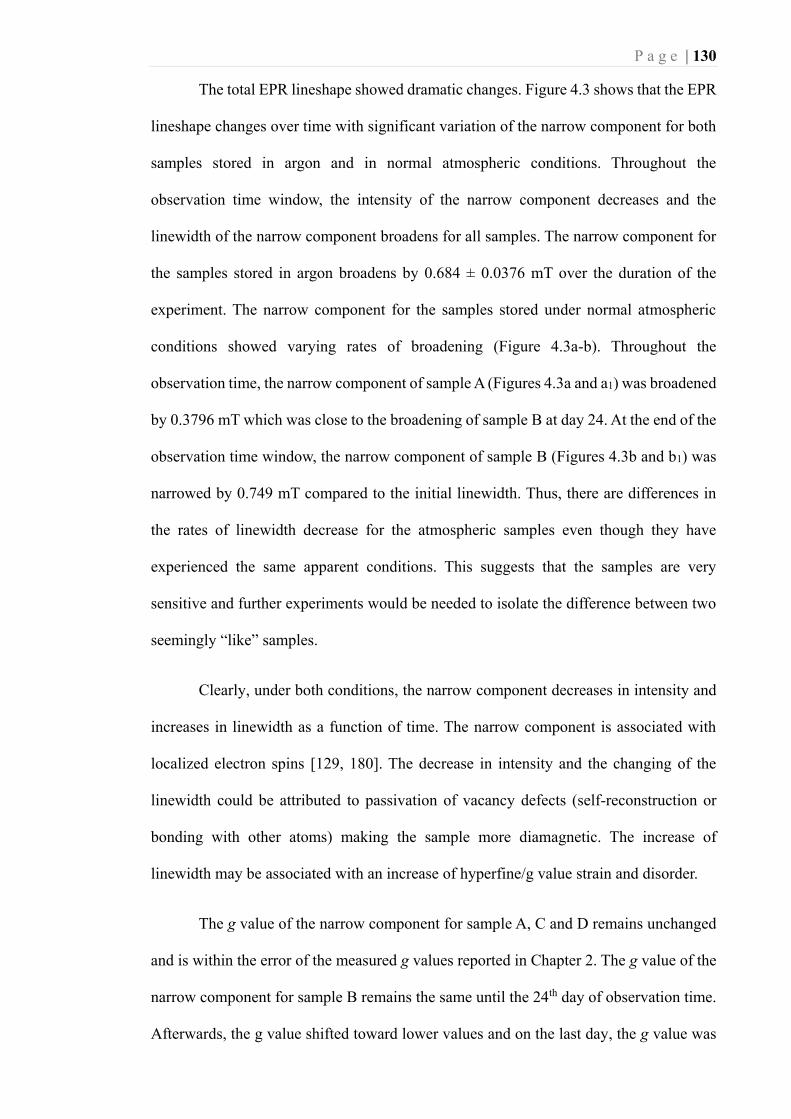
Figure 4.3 EPR lineshape evolution at room temperature and 𝐻∥ the orientation of
graphene laminate samples stored throughout 60 days. Samples stored under normal
atmospheric conditions (a and b); samples stored under argon (c and d). Time zero
spectra are shown in black. Spectra recorded at increasing duration are lighter in
colour (black to red to yellow). The a1, b1, c1 and d1 represent the lineshape at time
zero (black) and lineshape at 60th day (bright yellow). ......................................... 129
Figure 4.4 The evolution of mean total spin concentration throughout storage time. a)
normal spin concentration vs time. b) 1/log (spin concentration) vs log time. The
blue dot represents samples stored in normal atmospheric conditions; the red dot
represents samples stored in argon. ....................................................................... 132
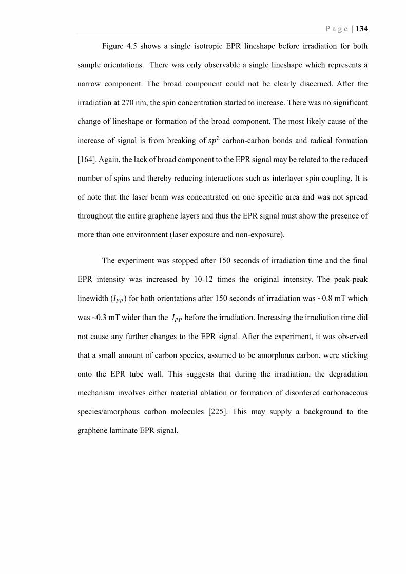
Figure 4.5 EPR spectra evolution of an aged graphene laminate after irradiation at 270
nm at room temperature. (a) The sample is positioned (𝐻⊥ ). (b) The sample is
positioned (𝐻∥). ..................................................................................................... 133
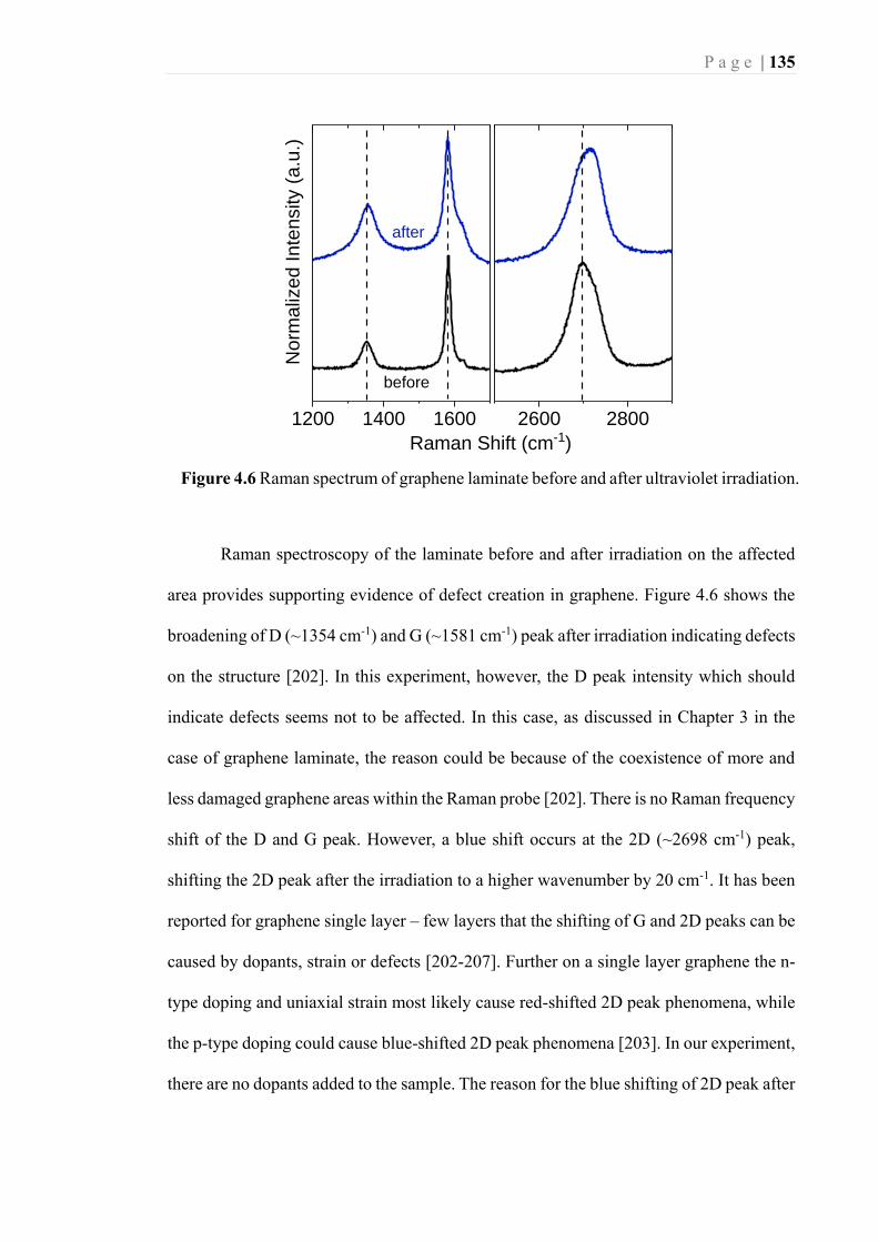
Figure 4.6 Raman spectrum of graphene laminate before and after ultraviolet irradiation.
............................................................................................................................... 135
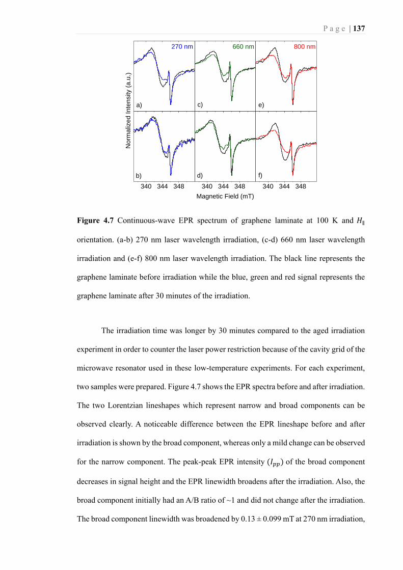
Figure 4.7 Continuous-wave EPR spectrum of graphene laminate at 100 K and 𝐻∥
orientation. (a-b) 270 nm laser wavelength irradiation, (c-d) 660 nm laser
wavelength irradiation and (e-f) 800 nm laser wavelength irradiation. The black line
represents the graphene laminate before irradiation while the blue, green and red
signal represents the graphene laminate after 30 minutes of the irradiation. ........ 137
Page 16
P a g e | 15
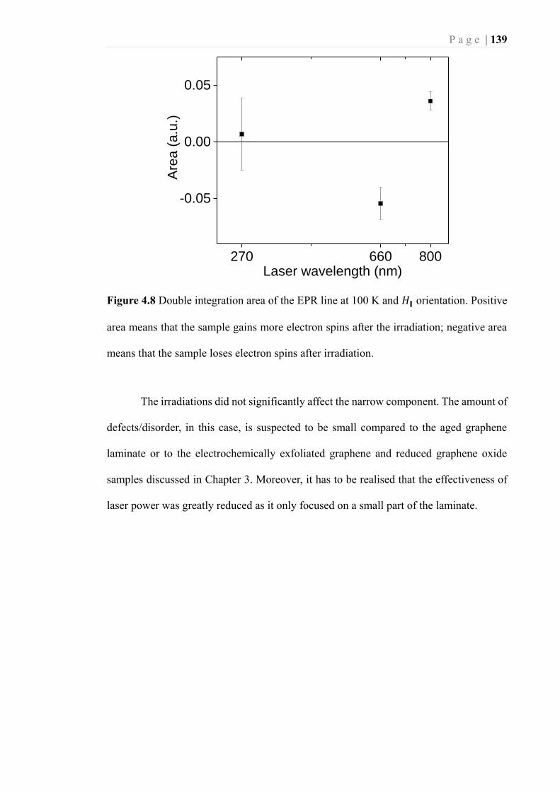
Figure 4.8 Double integration area of the EPR line at 100 K and 𝐻∥ orientation. Positive
area means that the sample gains more electron spins after the irradiation; negative
area means that the sample loses electron spins after irradiation. ......................... 139
Figure 4.9 Raman spectrum of graphene laminate before (black line) and after 30 minutes
of irradiation using a 270 nm laser (blue line), 660 nm laser (green line) and 800 nm
laser wavelengths (red line). ................................................................................. 140
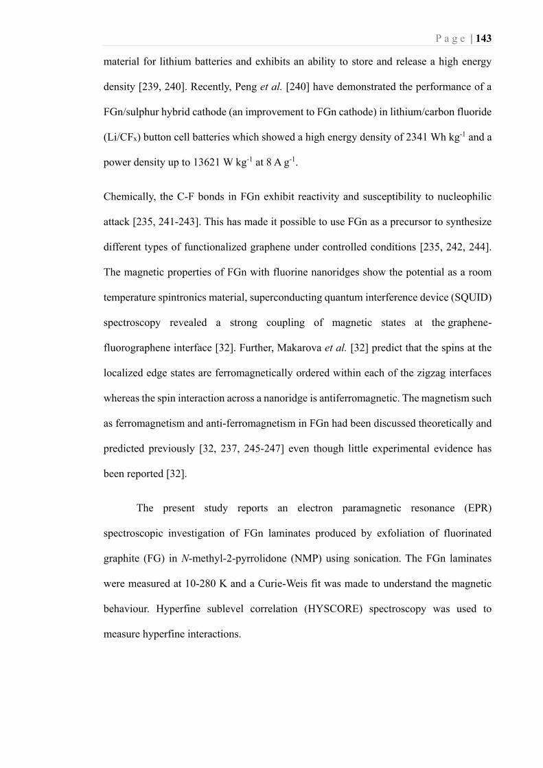
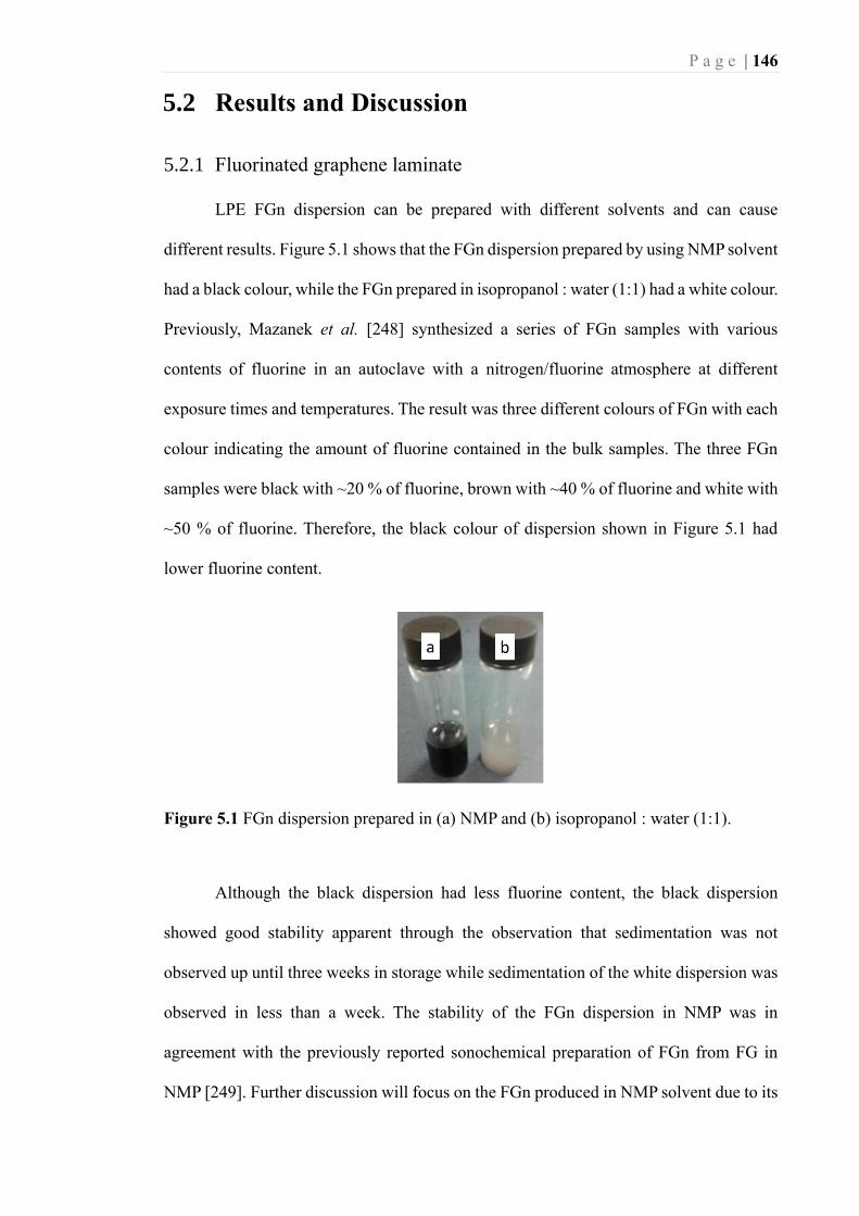
Figure 5.1 FGn dispersion prepared in (a) NMP and (b) isopropanol : water (1:1). .... 146
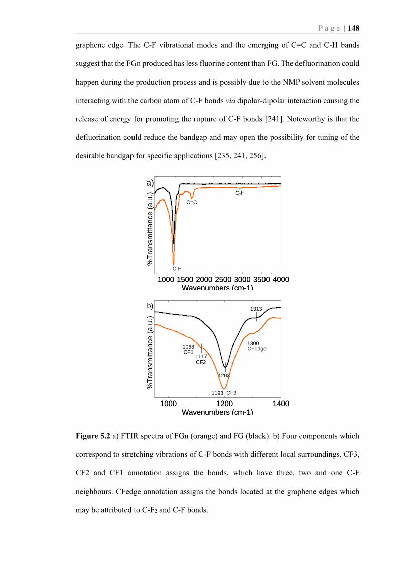
Figure 5.2 a) FTIR spectra of FGn (orange) and FG (black). b) Four components which
correspond to stretching vibrations of C-F bonds with different local surroundings.
CF3, CF2 and CF1 annotation assigns the bonds, which have three, two and one C-
F neighbours. CFedge annotation assigns the bonds located at the graphene edges
which may be attributed to C-F2 and C-F bonds. .................................................. 148
Figure 5.3 a) Raman spectra of FGn with 325 nm laser. b) Raman spectra of LPE
graphene (black) and FGn (blue) with 514.5 nm laser. ......................................... 149
Figure 5.4 The EPR lineshape of FGn laminate at 𝐻⊥ (solid black) and 𝐻∥ (solid blue)
simulated using a single Lorentzian lineshape (dash purple and orange). The
simulation was performed using easypin [176]. ................................................... 151
Figure 5.5 The evolution of EPR linewidth on the variation of temperature. The black
rectangle represents the 𝐻⊥ orientation and the red triangle represents the 𝐻∥
orientation. ............................................................................................................ 152
Figure 5.6 The evolution of double integrated EPR intensity ( 𝜒𝐸𝑃𝑅 ) on a wide
temperature range (300 – 10 K). Black rectangle represents the 𝐻⊥ orientation and
red rectangle represents the 𝐻∥ orientation. ......................................................... 153
Page 17
P a g e | 16
Figure 5.7 The Curie-Weis line fit for 𝐻⊥ orientation (solid black line) and 𝐻∥ orientation
(solid red line) at the temperature range of 100 – 10 K. The black rectangle and red
triangle represent 𝜒𝐸𝑃𝑅 at the 𝐻⊥ and 𝐻∥ orientations, respectively. .................. 154
Figure 5.8 The Curie-Weis line fit for 𝐻⊥ orientation (solid black line) and 𝐻∥ orientation
(solid red line) at the temperature range of 280 – 230 K. The black rectangle and red
triangle represent 𝜒𝐸𝑃𝑅 at the 𝐻⊥ and 𝐻∥ orientations, respectively. ................ 155
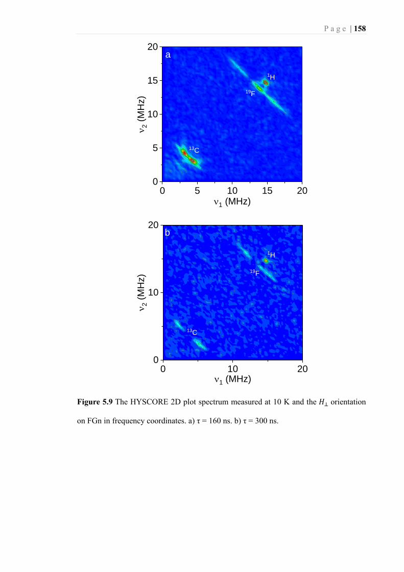
Figure 5.9 The HYSCORE 2D plot spectrum measured at 10 K and the 𝐻⊥ orientation
on FGn in frequency coordinates. a) τ = 160 ns. b) τ = 300 ns. ............................ 158
Figure 5.10 The HYSCORE 2D plot spectrum measured at 10 K and the 𝐻∥ orientation
on FGn in frequency coordinates. a) τ = 160 ns. b) τ = 300 ns. ............................ 159
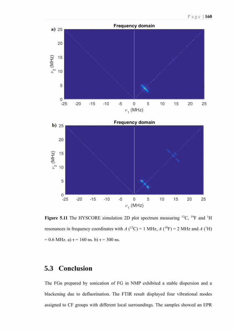
Figure 5.11 The HYSCORE simulation 2D plot spectrum measuring 13C, 19F and 1H
resonances in frequency coordinates with A (13C) = 1 MHz, A (19F) = 2 MHz and A
(1H) = 0.6 MHz. a) τ = 160 ns. b) τ = 300 ns. ....................................................... 160
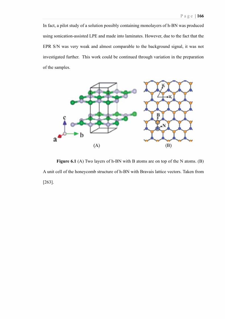
Figure 6.1 (A) Two layers of h-BN with B atoms are on top of the N atoms. (B) A unit
cell of the honeycomb structure of h-BN with Bravais lattice vectors. Taken from
[263]. ..................................................................................................................... 166
Page 18
P a g e | 17
Tables
Table 1 CW EPR studies on graphene materials. ........................................................... 60
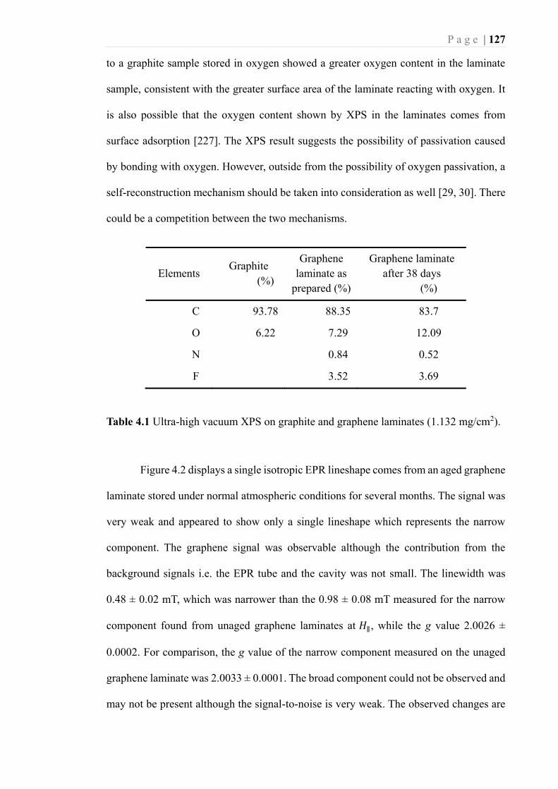
Table 4.1 Ultra-high vacuum XPS on graphite and graphene laminates (1.132 mg/cm2).
............................................................................................................................... 127
Page 19
P a g e | 18
List of Abbreviations
⊥ Perpendicular
∥ Parallel
2D Two dimensional
A Ampere (electrical current unit)
𝐴 Hyperfine coupling constant
AFM Atomic force microscope
ATR Attenuated total reflectance
A/B the ratio describing the symmetry of an EPR line
Å Angstrom (1 Å = 10-10 m)
𝛼 Opacity
𝐵0 External magnetic field
𝑐 The speed of light (299792458 m/s)
C Curie constant
CESR Conduction electron spin resonance
cm Centimeter (1 cm = 10-2 m)
DPPH 2,2-diphenyl-1-picrylhydrazyl
CVD Chemical vapour deposition
CW Continuous wave
oC Celcius
DMA N, N-dimethylacetamide
DMEU 1,3-dimethyl-2-Imidazolidinone
Δ𝐸 Energy difference between two eeeman split states
𝑒 Electron charge
EC Electrochemical exfoliation
𝐸𝐹 Fermi level
EM Electromagnetic
EPR Electron paramagnetic resonance
ESEEM Electron spin echo envelope modulation
ESR Electron spin resonance
eV Electron volt (1 eV = 1.602 x 10⁻¹⁹ J)
FG Fluorinated graphite
FGn Fluorinated graphene
Page 20
P a g e | 19
FID Free-induction decay
FLG Few layer graphene
FMR Ferromagnetic resonance
FTIR Fourier-transform infrared
g Gram (mass)
G Gauss (magnetic flux density/induction unit)
𝑔𝑒 g value of free electron (2.0023193043617)
GHz Gigahertz (1 GHz = 109 Hz)
GNRs Graphene nanoribbons
GO Graphene oxide
GPa Gigapascal (1 GPa = 109 Pa)
𝐻 External magnetic field
ℎ Planck’ constant (6.62607015 x 10⁻³⁴ kg m2 / s)
HOPG Highly oriented pyrolitic graphite
HRTEM High resolution transmission electron microscopy
HYSCORE The hyperfine sublevel correlation
Hz Hertz (1 Hz = 1 cycle per second)
ℏ Reduced Planck’s constant (ℏ = ℎ 2𝜋⁄ )
I Nuclear spin
𝐼𝐷 The Raman intensity of D band
𝐼𝐷′ The Raman intensity of D’ band
𝐼𝐺 The Raman intensity of G band
𝐼𝑃𝑃 Peak-peak EPR intensity
ITO Indium tin oxide
J Joule (unit of energy) (1 J = 1 Nm = 1 kg m2 / s2)
K Kelvin
kg Kilogram (mass) (1 kg = 1000 g)
kHz KiloHertz (1 kHz = 1000 Hz)
kV Kilovolt (1 kV = 1000 Volt)
L Litre
LPE Liquid phase exfoliation
m Meter
mA Milliampere (1 mA = 10-3 A)
MBE Molecular beam epitaxy
mg Milligram (1 mg = 10-3 g)
Page 21
P a g e | 20
MHz Megahertz (1 MHz = 106 Hz)
ml Millilitre (1 ml = 10-3 L)
mm Millimeter (1 mm = 10-3 m)
mN MilliNewton (1 mN = 10-3)
ms Millisecond (1 ms = 10-3 s)
𝑚𝑆 Spin quantum number
mT MilliTesla (1 mT = 10-3 T = 10 G)
mW MilliWatt (1 mW = 10-3 W)
𝜇 Electron magnetic moment
𝜇𝐵 Bohr magneton constant (9.274009994 x 10⁻²⁴ J T-1)
µm Micrometre (1 µm = 10-6 m)
N Newton (1 N = 1 kg m/s2)
NIR Near infrared
NIT nitronyl nitroxide
nm Nanometre (1 nm = 10-9 m)
NMP 1-methyl-2-pyrrolidinone
ns Nanosecond (1 ns = 10-9 s)
OLEDs Organic light-emitting diodes
OPO Optical parametric oscillator
o-DCB Orthodichlorobenzene
Ω Ohm (electron resistance unit)
Pa Pascal (1 Pa = 1 N/m2)
PC Propylene carbonate
PDMS Polydimethylsiloxane
PMMA Polymethyl methacrylate
PVD Physical vapour deposition
rGO Reduced graphene oxide
𝑅2 Coefficient of determination
s Second (time)
S Siemens (electron conductance unit; 1 S = 1 Ω−1)
𝑆 Spin angular momentum
SDBS Sodium dodecylbenzenesulfonate
SLG Single layer graphene
SQUID Superconducting quantum interference device
S/N Signal to noise ratio
Page 22
P a g e | 21
𝑡 Pulse delay
T Tesla (magnetic flux density/induction unit; 1 Tesla = 10000 G)
𝑇1 Spin-lattice relaxation time
𝑇2 Spin-spin relaxation time
𝑇𝐶 Curie temperature
𝑇𝑀 Phase memory time
𝑇𝑀(𝑁)
Nucleus phase memory time
𝑇𝑁 Néel temperature
TEM Transmission electron microscope
TPa Terapascal (1 TPa = 1012 Pa)
𝜏 Pulse delay at which the echo is detected
𝜃 Curie-Weiss constant
UHV Ultra high vacuum
UV Ultra violet
V Volt
Vis Visible
𝜈 Electromagnetic irradiation frequency
W Watt (unit of power) (1 W = 1 J/s)
Wh Watt-hour (1 Wh = 3600 Joule)
XPS X-ray photoelectron spectroscopy
𝜒 Magnetic susceptibility
Page 23
P a g e | 22
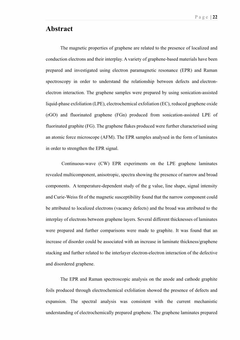
Abstract
The magnetic properties of graphene are related to the presence of localized and
conduction electrons and their interplay. A variety of graphene-based materials have been
prepared and investigated using electron paramagnetic resonance (EPR) and Raman
spectroscopy in order to understand the relationship between defects and electron-
electron interaction. The graphene samples were prepared by using sonication-assisted
liquid-phase exfoliation (LPE), electrochemical exfoliation (EC), reduced graphene oxide
(rGO) and fluorinated graphene (FGn) produced from sonication-assisted LPE of
fluorinated graphite (FG). The graphene flakes produced were further characterised using
an atomic force microscope (AFM). The EPR samples analysed in the form of laminates
in order to strengthen the EPR signal.
Continuous-wave (CW) EPR experiments on the LPE graphene laminates
revealed multicomponent, anisotropic, spectra showing the presence of narrow and broad
components. A temperature-dependent study of the g value, line shape, signal intensity
and Curie-Weiss fit of the magnetic susceptibility found that the narrow component could
be attributed to localized electrons (vacancy defects) and the broad was attributed to the
interplay of electrons between graphene layers. Several different thicknesses of laminates
were prepared and further comparisons were made to graphite. It was found that an
increase of disorder could be associated with an increase in laminate thickness/graphene
stacking and further related to the interlayer electron-electron interaction of the defective
and disordered graphene.
The EPR and Raman spectroscopic analysis on the anode and cathode graphite
foils produced through electrochemical exfoliation showed the presence of defects and
expansion. The spectral analysis was consistent with the current mechanistic
understanding of electrochemically prepared graphene. The graphene laminates prepared
Page 24
P a g e | 23
using electrochemical exfoliation and reduced graphene oxide showed similar spectral
characteristics and the contribution of localized and conduction electrons for each type of
graphene laminate were identified and characterized. There was evidence to suggest that
the coupled and decoupled states of localized and itinerant conduction electrons were also
influenced by defects and functionalization.
The paramagnetic stability and defects of graphene laminate samples induced by
ageing and action of a nanosecond pulsed laser irradiation were investigated. Ageing of
graphene laminates showed a reduction in the EPR intensity with time in both
atmospheric and argon atmospheres indicating passivation. Laser irradiation of the aged
sample caused an increase in the numbers of spins whereas a reduction was observed for
unaged samples. It was shown that the defects created by the laser could break the 𝑠𝑝2
carbon-carbon bonds and create new spin centres.
EPR spectroscopy of FGn revealed an isotropic line shape indicative of a
homogeneously broadened EPR resonance arising from electron-electron interactions.
The Curie-Weiss fit of the magnetic susceptibility behaviour showed two temperature
regions, which show the magnetic moments to couple both ferromagnetically and
antiferromagnetically. Hyperfine sublevel correlation (HYSCORE) spectroscopy was
able to measure the fluorine hyperfine interaction.
Page 25
P a g e | 24
Declaration
I declare that no portion of this work referred to in this thesis has been submitted in
support of an application for another degree or qualification of this or any other university
of other institutes of learning.
Manchester.
Date: 25/09/2019
Signed:
Oka P. Arjasa
Page 26
P a g e | 25
Copyright Statement
i. The author of this thesis (including any appendices and/or schedules to this thesis) owns
certain copyright or related rights in it (the “Copyright”) and s/he has given The
University of Manchester certain rights to use such Copyright, including for
administrative purposes.
ii. Copies of this thesis, either in full or in extracts and whether in hard or electronic copy,
may be made only in accordance with the Copyright, Designs and Patents Act 1988 (as
amended) and regulations issued under it or, where appropriate, in accordance with
licensing agreements which the University has from time to time. This page must form
part of any such copies made.
iii. The ownership of certain Copyright, patents, designs, trademarks and other intellectual
property (the “Intellectual Property”) and any reproductions of copyright works in
the thesis, for example, graphs and tables (“Reproductions”), which may be described
in this thesis, may not be owned by the author and may be owned by third parties. Such
Intellectual Property and Reproductions cannot and must not be made available for use
without the prior written permission of the owner(s) of the relevant Intellectual Property
and/or Reproductions.
iv. Further information on the conditions under which disclosure, publication and
commercialisation of this thesis, the Copyright and any Intellectual Property and/or
Reproductions described in it may take place is available in the University IP Policy
(see http://documents.manchester.ac.uk/DocuInfo.aspx?DocID=24420), in any relevant
Thesis restriction declarations deposited in the University Library, The University
Library’s regulations (see http://www.library.manchester.ac.uk/about/regulations) and
in the University’s policy on Presentation of Theses.
Page 27
P a g e | 26
Acknowledgements
All the praises and thanks be to Allah (God) which made all of this possible. Also,
it would not have been possible to write this doctoral thesis without the help and support
of the kind people around me, to only some of whom it is possible to give particular
mention here.
This thesis would not have been possible without the help, support and patience
of my principal supervisor Dr Alistair J. Fielding, not to mention his advice and discussion
for which I’m extremely grateful. Also, the good advice and support of my second and
third supervisor, Prof. Cinzia Casiraghi and Prof. Eric Mcinnes, which have been
invaluable on both an academic and a personal level.
I would also like to thank all the members/staff of the EPR and graphene groups,
in particular to Bin Wang, Tong Jincheng, Dr Khaled Parvez, Dr Ana Maria Ariciu, Lidya
Nodaraki, Dr Yu Young Shin, Dr Daniele Rizzo, Adam Brookfield, Dr Guillem Brandariz
de Pedro, Lara Grangel Gutierrez, Marco earattini, Dr Daryl Mcmanus, Dr Floriana Tuna
and Prof. David Collison.
I would like to acknowledge the financial support of the Indonesian Ministry of
Research, Technology and Higher Education and as well as the Agency for the
Assessment and Application of Technology (BPPT), particularly in the award of a
postgraduate scholarship.
Lastly and most importantly, I would like to express my love and gratitude to my
mother Tri Wuryani and my father Dr Wayan Sabe Arjasa, may you both rest in peace. To
my wife Primalia Swariputri and my son eayn Lorentzian Al-Razi Arjasa, for giving me
happiness.
Page 28
P a g e | 27
1. CHAPTER ONE
Introduction
1.0 Graphene
The carbon atom has two stable isotopes, 12C (98.9%, nuclear spin I = 0) and 13C
(1.1%, nuclear spin I = 1 2⁄ ) [1]. All carbon-based materials exist in different allotropes
such as graphite, diamond, carbon nanotube, graphene etc. Graphene is a single-atomic
layer made of carbon atoms with sp2 hybridization. Graphene is a two-dimensional
material, i.e. a material having a structure of a single layer of atoms. Graphene was
isolated for the first time in 2004 [2], previously it was believed to be too difficult to
isolate due to the thought that it was unstable at normal atmospheric conditions and the
lack of information on its properties [3, 4]. Graphene is considered as the basic structural
unit in sp2 carbon materials as shown in Figure 1.1 [5] i.e. graphene can be rolled or
stacked to form carbon nanotubes or graphite.
Figure 1.1 Schematic illustration showing that graphene can be rolled or stacked to form
different carbon-based nanomaterials. Taken from [5].
Page 29
P a g e | 28
1.1 Properties of graphene
Graphene has a long list of outstanding properties. The most remarkable is not
only the electronic properties but also its mechanical and optical properties for several
applications. Graphene is the thinnest material (one atom thick) and has an estimated
Young’s modulus of 2.4 ± 0.4 TPa [6]. It has breaking strength of 42 N/m (on a defect-
free sheet) with a tensile strength of 130 GPa [7] and room temperature thermal
conductivity in the range (4.84 ± 0.44) x 103 to (5.3 ± 0.48) x 103 W/mK [8].
The electrons in the π-orbital of graphene behave like particles with no mass,
giving rise to extremely high charge mobility of 250.000 cm2 V-1 s-1 at room temperature,
making graphene the crystal with the highest charge mobility [9]. Graphene is a zero-gap
semiconductor where the conduction band and the valence band touch at the Dirac point
[10]. The armchair and zig-zag edges of graphene (Figure 1.2) may be related to its
magnetic properties [11].
Figure 1.2 Schematic showing the two types of edges in graphene, the armchair edges
and the zigzag edges. Taken from [12].
Graphene is also almost transparent in the visible range, Nair et al. showed that
single-layer graphene absorbs 2.3 % of the incident light, and the opacity is practically
Page 30
P a g e | 29
independent of wavelength (Figure 1.3B). The absorption of light is proportional to the
number of layers. Figure 1.3A shows an image of an aperture that is partially covered by
suspended graphene to compare the opacities of different areas [13].
Figure 1.3 (A) Photograph of a 50 μm aperture partially covered by mono and bilayer
graphene. The line scan profile shows the intensity of the transmitted white light along
the yellow line. The inset shows a metal support structure with different sizes of aperture.
(B) Transmittance spectrum of single-layer graphene (open circles). The red and green
line is the theoretical transmittance expected for ideal Dirac electrons and graphene,
respectively. The inset shows the transmittance of white light as a function of the number
of graphene layers. Taken from [13].
Magnetic behaviour in graphene is associated with the interaction of the localized
and itinerant conduction electron spins [14-21]. Magnetism in graphene may arise from
impurities (i.e. adatoms) and active defects (i.e. in-plane vacancy defects / dangling bonds,
non-bonding edge defects) [22-24]. Active defects are often described as a preliminary
condition for the existence of magnetic order [25-27]. However, active defects may not
last long in normal conditions due to self-reconstruction and passivation by other
atoms/molecules [28-30]. Interestingly according to theoretical studies, edge states
Page 31
P a g e | 30
consisting of nonbonding π-electrons located at the edge region [11] are often discussed
with regard to their contribution to the paramagnetic activities of graphene [31-33]. The
unpaired electron at the zig-zag edges (Figure 1.2) on graphene may spin-polarized and
could arrange parallel to each other [31-33]. The magnetic properties of different types of
graphene samples, with different properties, have been experimentally investigated [16, 19-
22, 28, 34-37]. A full report of the state-of-the-art developments is provided in Section 1.4.2.
1.2 Applications of graphene
Because of its outstanding mechanical, optical and electrical properties, graphene
can be used in several applications. In electronics, the high transmittance added with the
low sheet resistance of highly doped samples [38], allows graphene to be used as a
transparent conductive material in flexible electronics, such as in touch screen displays,
electronic paper and organic light-emitting diodes (OLEDs). Moreover, graphene has
better properties than indium tin oxide (ITO) due to its high mechanical flexibility and
chemical durability which are important characteristics for flexible electronic devices
[39]. The fracture strength of defect-free graphene is currently higher (the breaking
strength = 42 N m-1, Young’s modulus = 1 TPa) compared to many other conventional
materials [7] such as ITO (Young’s modulus = 0.116 TPa) [40], which make graphene
suitable for bendable and rollable devices [38].
In the case of transistors, graphene is gapless, so it cannot be used for digital
applications. However, for high-frequency transistor applications, graphene could be used,
but it has to compete against conventional semiconductor materials (III-V materials) [38,
41]. Graphene will probably be used when conventional semiconductor materials fail to
satisfy device requirements [38].
Page 32
P a g e | 31
As discussed, graphene in principle has a wavelength-independent absorption of
2.3% [13] in the near IR-visible range. This property makes graphene suitable as a
material used in photodetectors [42]. Moreover, high carrier mobility in graphene enables
high bandwidth operation up to 640 GHz [38, 43]. Currently, the poor responsivity arising
from the very small absorption of light has hindered graphene application in
photodetectors. Photocurrent sensitivity can be increased in several ways such as coupling
the graphene with another material i.e. gold [44], using stacked monolayer graphene
separated by a thin tunnel barrier [45], or by increasing light-graphene interaction with a
waveguide [46]. Operating at a bandwidth of ~100 GHz, InGaAs and Ge are more
favourable compared to graphene in photodetector applications at the moment. Therefore,
it is predicted that graphene photodetectors will be competitive in the future providing
that the issues related to it are solved [38]. Another potential graphene application in
photonic devices is as the saturable absorber of mode-locked lasers [pulses of a laser in
extremely short duration in the order of picoseconds (10-12 s) or femtoseconds (10-15 s)]
[47]. Compared to other semiconductor saturable absorbers, the benefits of graphene as a
saturable absorber are: graphene reaches saturation at a lower intensity over a wide
spectral range [48], has ultrafast carrier relaxation times, has controllable modulation
depth [13, 38], and has high thermal conductivity [8].
In terms of energy storage applications, graphene as an active medium in solar
cells would benefit from uniform absorption over a broad spectrum [13], but on the other
hand, it would also suffer from low optical absorption [13] that it would require dopant
enhancement structures [44]. However, doped graphene as an electrode in dye-sensitized
solar cells has proved highly beneficial. Graphene electrodes, depending on the dopants,
can be used as electron/n-type [49] or hole/p-type [50] conducting mediums.
Graphene can be modified to form nanostructured materials which have relatively
high surface areas and thus have the potential to be used in energy storage applications
Page 33
P a g e | 32
such as in lithium-ion batteries [51]. The high surface area allows an increase of the ion
transfer efficiency, therefore the use of graphene could reduce the amount of electrode
materials needed without reducing the power output. The high surface area of
nanostructured graphene-based materials is also applicable for sodium-ion batteries [52]
and supercapacitors [53, 54] which have shown an increase of the specific energy density
(Wh/kg). The high thermal conductivity of graphene [8] may be a benefit when it comes
to high current loads that generate heat such as in the battery system [38]. This would
help applications that require cooling (e.g. electronics).
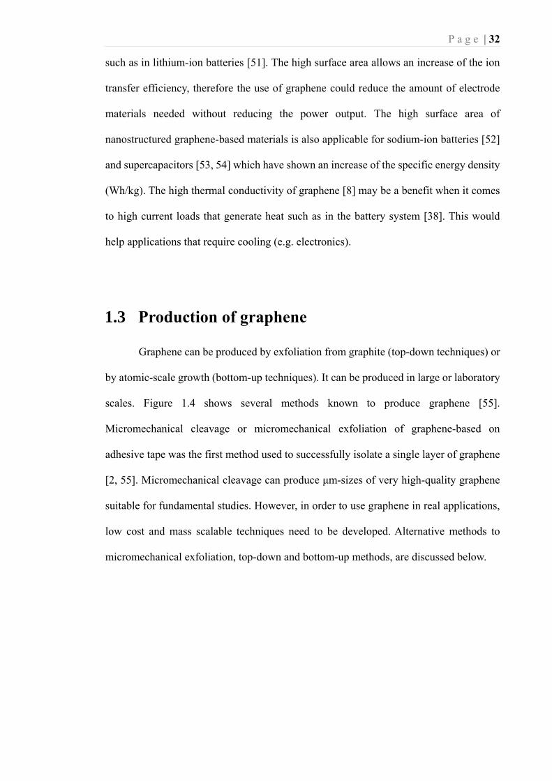
1.3 Production of graphene
Graphene can be produced by exfoliation from graphite (top-down techniques) or
by atomic-scale growth (bottom-up techniques). It can be produced in large or laboratory
scales. Figure 1.4 shows several methods known to produce graphene [55].
Micromechanical cleavage or micromechanical exfoliation of graphene-based on
adhesive tape was the first method used to successfully isolate a single layer of graphene
[2, 55]. Micromechanical cleavage can produce μm-sizes of very high-quality graphene
suitable for fundamental studies. However, in order to use graphene in real applications,
low cost and mass scalable techniques need to be developed. Alternative methods to
micromechanical exfoliation, top-down and bottom-up methods, are discussed below.
Page 34
P a g e | 33
Figure 1.4 Methods for producing graphene. Each of them has its own advantages and
disadvantages related to graphene size, quality and application purposes. Taken from [55].
1.3.1 Anodic bonding
Anodic bonding (Figure 1.4b) consists of placing graphite onto a glass substrate
and applying a high voltage (0.5-2 kV) between the graphite and the metal back contact.
A positive voltage is applied on the graphite side, and then the glass substrate is heated
(~200 oC for 10-20 minutes). A few layers of graphene stick to the glass due to
Page 35
P a g e | 34
electrostatic interactions of ions in the glass and can be cleaved afterwards [55, 56].
Anodic bonding is able to produce graphene with a lateral size of 20-30 μm.
1.3.2 Photo exfoliation
The photo exfoliation technique (Figure 1.4c) uses pulsed laser irradiation
(typically 800 nm wavelength) in a vacuum or inert conditions to minimize the oxidation
of graphene [57, 58]. The irradiation results in the detachment of an entire or partial layer
of graphite. The energy density required increases with the decreasing number of
graphene layers obtained, up to ~7 layers of graphene can be obtained. This new method
is still in need of further development [55, 58].
1.3.3 Liquid phase exfoliation
Liquid phase exfoliation (LPE) (Figure 1.4d) allows exfoliation of graphite in a
liquid environment. The liquid is either water [59, 60] or an organic solvent [61, 62]. In
general, the process consists of three steps, dispersion of graphite in a liquid, exfoliation,
and purification or separation of graphene flakes from the remaining of graphite flakes.
The exfoliation process is typically done in a bath sonicator, where the formation,
growth, and collapse of bubbles or voids in liquids due to pressure fluctuations of the
sound wave will induce exfoliation [55]. The shear forces created from the collapse of
bubbles between the layers of graphite can break the π-π interaction (inter-layer
interaction) and exfoliate the layers. After the exfoliation, it is important to balance the
inter-sheet attractive forces, therefore suitable solvents need to be identified. If the
interfacial tension between the liquid and graphitic flakes is high, the adhesion (i.e. the
energy per unit area required to separate two surfaces from one interface) between them
is low, and the dispersibility of graphene flakes is poor. It was shown that solvents with
Page 36
P a g e | 35
the surface tension of ~ 40 mN/m are those providing the highest amount of exfoliated
graphene [61]. Thus, solvents such as 1-methyl-2-pyrrolidinone (NMP), benzyl benzoate,
1,3-dimethyl-2-imidazolidinone (DMEU), and N, N-dimethylacetamide (DMA) are good
for exfoliation and stabilization of graphene [61]. However, all of these solvents have
some disadvantages: they are toxic, and all of them have high boiling points, making it
difficult to remove them after exfoliation. Alternatively, low boiling point solvents such
as isopropanol, acetone, ethanol, etc. can be used, but they give very low yields compared
to organic solvents. Water, a non-toxic and mild boiling point solvent with a surface
tension of 72 mN/m, is not suitable for LPE. In order to produce graphene dispersions in
water, two methods can be used:
(i) A suitable amphiphilic molecule can be used to help stabilise the graphitic flakes
in water, e.g. sodium dodecylbenzenesulfonate (SDBS) [59] and 1-pyrenesulfonic acid
[63].
(ii) The starting graphitic is oxidised, turning the material from hydrophobic to
hydrophilic because of the C-O groups formed on the surface. Graphite oxide can be
easily exfoliated in water leading to the production of graphene oxide (GO). GO shows
very different properties from graphene because of numerous oxygen species
functionalization. GO can be reduced thermally and/or chemically to produce reduced
graphene oxide (rGO) (see Section 1.3.5 for a more detailed discussion).
The liquid phase exfoliation method is an important technique because it allows
high production capacity and high concentration of graphene. The quality of graphene
produced by LPE, although it cannot compare to mechanical exfoliation methods, is
relatively good with a competitive production cost if compared to other methods capable
to produce graphene in large scale. Coleman et al. demonstrated that sonication of
graphite doesn’t cause any basal plane defects on graphene [64-68]. Their argument is
based on the observed Raman D band of thin films, prepared from vacuum filtration of
Page 37
P a g e | 36
sonication-assisted LPE graphene, which is assumed due to edge defects. They suggested
if the assumption was true, then the average ID IG⁄ ratio should scale to the flake edge to
area ratio: ID IG ∝ [L−1 + w−1]⁄ , where L and w are average length and width of the
graphene flakes, respectively [64]. The prediction was in agreement with their results
indicate that the observed Raman D band was from edge defects [69]. However, several
other studies suggest that ultrasonication does introduce defects in the basal plane of
graphene. The X-ray photoelectron spectroscopy (XPS) analysis carried out by Skaltsas
et al. on NMP and orthodichlorobenzene (o-DCB) LPE graphene produced at different
tip sonication power and times showed high oxygen content present as carboxylic acid
and ether/epoxy functional groups on the graphene lattice as a result of sonication [70].
The effect of bath sonication times on defect localisation has been studied by Bracamonte
et al. which suggests that defects observed for short sonication times were mainly from
edge defects, whereas longer sonication times (> 2 hours) caused basal plane defects.
They also suggested that the observed basal plane defects are not sp3-like or vacancies or
substitutional impurities but topological defects (like pentagon-heptagon pairs) due to a
roughly constant 𝐼𝐷 𝐼𝐷′⁄ ratio of 4.5 ± 0.5 [71] and since they tend to have the lowest
formation energy [72].
1.3.4 Electrochemical exfoliation
The electrochemical exfoliation (EC) technique typically uses electric current to
trigger ion intercalation, structural expansion and exfoliation of graphite working
electrodes in a liquid electrolyte via cathodic reduction or anodic oxidation reaction. The
anodic and cathodic exfoliation are the two main strategies of the EC method and both
have their own advantages and disadvantages. Anodic exfoliation is most commonly used
because the exfoliation can be readily carried out in water using simple electrolytes (e.g.
Page 38
P a g e | 37
sulphate-based) to produce graphene (1-3 layers thick) in high yield [73, 74]; whereas,
cathodic exfoliation is a slow process and in some cases requires sonication to exfoliate
the already expanded graphite. However, the graphene flakes produced from the
exfoliation of graphite cathode have a lower degree of surface oxidation (typically the
graphene produced has 2.3 wt% increase of oxygen content [75]) or functionalization,
thereby retaining the typical properties of graphene [73].
(i) Anodic exfoliation
The exfoliation for the anodic route is mostly performed in an aqueous electrolyte.
The mechanism of anodic electrochemical exfoliation using sulfate ions can be divided
into three stages [76] and the schematic illustration of the exfoliation is shown in Figure
1.5.
Figure 1.5 Schematic mechanism of anodic electrochemical exfoliation taken from [76].
The first stage consists of a reduction of water at the cathode due to bias voltage,
creating hydroxyl ions [OH−] that act as a strong nucleophile in the electrolyte and
initially attack graphite at the edge sites and grain boundaries. The second stage consists
of oxidation at the edge sites and grain boundaries and then leads to depolarization and
expansion of the graphite layers, thereby facilitating the intercalation of sulfate ions
Page 39
P a g e | 38
[SO42−] within the graphitic layers. During this stage, water molecules may co-intercalate
with the [SO42−] anions. The third stage consists of reduction of [SO4
2−] anions and self-
oxidation of water to produce gaseous species such as SO2, O2, and others, as evidenced
by the vigorous gas evolution during the electrochemical process [77, 78]. These gaseous
species can exert large forces on the graphite layers, which are sufficient to separate
weakly bonded graphite layers from one another [79].
The sulfate ion is suitable for intercalation and exfoliation of graphite because: a)
the ionic size of sulfate ion (0.46 nm) is close to the graphite interlayer spacing (0.335
nm) [80]; b) the reduction of sulfate ion and the oxidation of water lead to the formation
of gaseous species i.e. SO2, O2, and H2, which could promote the exfoliation of graphene
sheets [81]. Ion intercalation in acidic electrolytes e.g. H2SO4 is so fast that it occurs
simultaneously with exfoliation at all graphite edges and the interplay between [H+] and
[SO42−] results in excess oxidation of graphene at low pH [74]. These problems can be
overcome by the use of melamine additives in sulfuric acid. Chen et al. demonstrate the
use of various melamine additives in aqueous acids (H2SO4 in deionized water) [82]. The
interplay between melamine and the basal plane of graphene was thought to facilitate
exfoliation and provides in-situ protection of the graphene flake surface against further
oxidation resulting in graphene with high C/O ratio (26.2), good uniformity (over 80 %
are less than 3 layers), and low defect density (𝐼𝐷 𝐼𝐺⁄ < 0.45) [82]. Another solution is to
use inorganic salts such as ammonium sulfate, sodium sulfate, and potassium sulfate
which have been previously investigated [76]. Among them, ammonium sulfate
represents the best performance which shows a good C/O ratio of 17.2 with over 80 %
thin graphene produced (consisting of 1-3 layers) and low defect density (𝐼𝐷 𝐼𝐺⁄ = 0.25)
[76].
Page 40
P a g e | 39
Non-aqueous electrolyte such as organic solution and ionic liquid (IL) could also
be used as the electrolyte. However, cost, safety and efficiency problems restricted the
development of the non-aqueous electrolyte [83].
(ii) Cathodic exfoliation
Unlike the anions intercalation in the anode exfoliation process, the kinetics of
cation intercalation in the cathode exfoliation process is slow [73]. Huang et al. tried to
accelerate the kinetics of the intercalation by using molten LiOH at 600 oC but this was
still not enough to achieve complete exfoliation of the graphite and sonication steps were
required in order to achieve reasonable yields of graphene (80 wt%) [84]. Although the
ion size of [Li+] is small (0.146 nm in diameter) [85] which should be favourable for the
intercalation, however, due to the slow kinetics of the intercalation, [Li+] alone could not
effectively expand the graphite cathode. In principle, incorporation of a [Li+] metal
complex i.e. [Li+]/propylene carbonate (PC) could intercalate into the interlayer space of
cathodic graphite effectively and cause an expansion of the graphite interlayer. However,
subsequent ultrasonication is still needed to achieve a 70 wt% yield of few-layer graphene
and the potentials required are in excess of -15 V [86]. Yang et al. demonstrate a cathodic
intercalation route that could directly exfoliate the graphite cathode by using N-butyl,
methylpyrrolidinium bis(trifluoromethylsulfonyl)imide. However, the potentials required
were around -30 V [87].
1.3.5 Reduced graphene oxide
One of the most popular methods to produce graphene is by oxidising the graphite
to generate graphite oxide which could easily be exfoliated by ultrasonication in various
solvents to produce graphene oxide (GO). The most commonly used method for oxidising
Page 41
P a g e | 40
graphite is the Hummers’ method, which includes strong oxidising agents like potassium
permanganate, nitric acid and sulfuric acid [88]. The oxidation results in epoxy, hydroxyl
and carbonyl group functionalization of the graphene. The functionalization increases the
graphite interlayer spacing and after subsequent sonication, the hydrophilic nature of the
functional groups facilitates excellent stability of GO in water [89]. GO is negatively
charged due to the ionisation of the functional groups which provides electrostatic
repulsion and increases GO stability in water, alcohols and certain organic solvents [90].
Reduced graphene oxide can be produced by reduction via chemical or thermal
methods. The chemical approach uses reducing agents such as hydrazine (N2H4) [91, 92],
sodium borohydride (NaBH4) [93, 94] and hydrogen iodide (HI) [95] etc. During the
reduction, the brown coloured GO turns black and precipitates in the solution. The
reduction process, however, could not remove the oxygen-containing species completely
and could not restore carbon sp2 hybridisation. Therefore leaving carbon sp3 hybridized
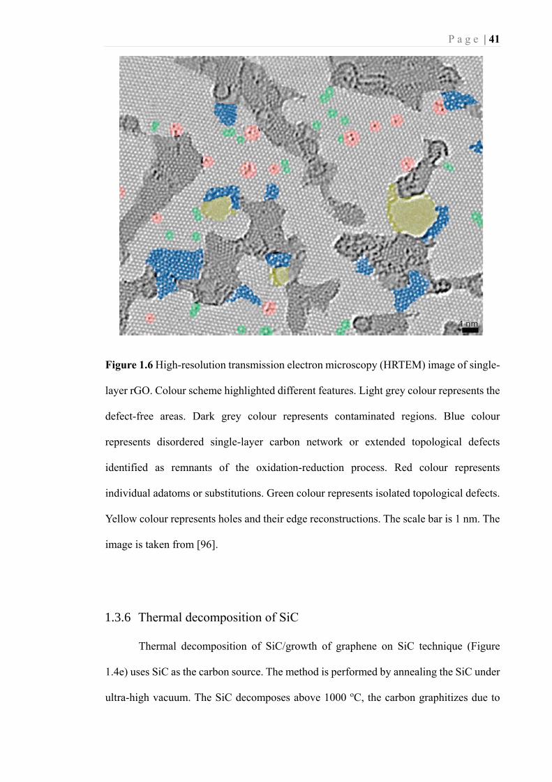
and vacancies [96] (Figure 1.6).
Heat treatment at high temperature could increase the efficiency of the restoration
process with dramatic reduction of surface defects and residual oxygen. Several studies
have demonstrated the restoration of sp2 carbon lattice by applying high temperature (≥
1500 oC) i.e. graphitisation. The obtained graphene showed improved electronic
properties with electron mobility ~1000 cm2/Vs (the precursor rGO had a value of 130
cm2/Vs) [97] and electrical conductivity of 577000 S/m [98].
Page 42
P a g e | 41
Figure 1.6 High-resolution transmission electron microscopy (HRTEM) image of single-
layer rGO. Colour scheme highlighted different features. Light grey colour represents the
defect-free areas. Dark grey colour represents contaminated regions. Blue colour
represents disordered single-layer carbon network or extended topological defects
identified as remnants of the oxidation-reduction process. Red colour represents
individual adatoms or substitutions. Green colour represents isolated topological defects.
Yellow colour represents holes and their edge reconstructions. The scale bar is 1 nm. The
image is taken from [96].
1.3.6 Thermal decomposition of SiC
Thermal decomposition of SiC/growth of graphene on SiC technique (Figure
1.4e) uses SiC as the carbon source. The method is performed by annealing the SiC under
ultra-high vacuum. The SiC decomposes above 1000 oC, the carbon graphitizes due to
Page 43
P a g e | 42
evaporation of Si. The problem that arises in this method is that the graphene grows on
SiC which has a different atomic structure compared to graphene. The mismatch of the
substrate is thought to lead to defects on the graphene produced [55].
1.3.7 Growth of graphene on metallic surfaces by precipitation
The growth of graphene on metallic surfaces by precipitation (Figure 1.4f) refers
to techniques allowing precipitation of carbon atoms on metal surfaces. The techniques
used are flash evaporation, physical vapour deposition (PVD), CVD, spin coating etc [55].
The carbon source is in the form of solid, liquid or gas. Carbon precipitation is affected
by the amount of pressure, temperature, annealing time, cooling rate and metal thickness
[99].
1.3.8 Chemical vapour deposition
Chemical vapour deposition (CVD) (Figure 1.4g) allows the growth of
polycrystalline graphene by depositing a mixture of hydrocarbon gas on a metal plate at
high temperature. The technique is proven to be promising and has been able to produce
square metres of graphene [39]. However, it does require a transfer/removal process as
the most cost-effective graphene produced so far is grown on inexpensive metals such as
copper, nickel and cobalt [99], which may not be a suitable substrate for many
applications. The high cost of production and the difficulty to control the grain size have
hindered the development of this technique.
The wet-transfer method is often used to transfer graphene from a metallic
substrate to other substrates. A well-known wet-transfer method uses polymethyl
methacrylate (PMMA) [100] or polydimethylsiloxane (PDMS) [101] to coat the graphene
Page 44
P a g e | 43
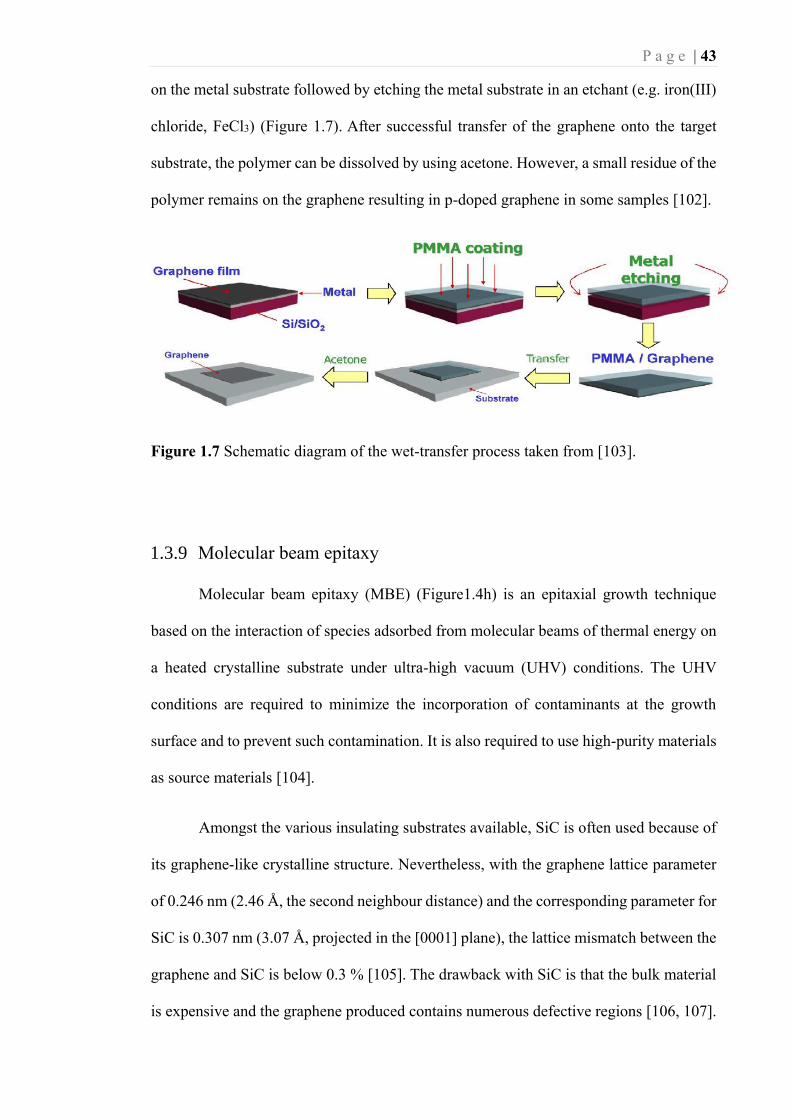
on the metal substrate followed by etching the metal substrate in an etchant (e.g. iron(III)
chloride, FeCl3) (Figure 1.7). After successful transfer of the graphene onto the target
substrate, the polymer can be dissolved by using acetone. However, a small residue of the
polymer remains on the graphene resulting in p-doped graphene in some samples [102].
Figure 1.7 Schematic diagram of the wet-transfer process taken from [103].
1.3.9 Molecular beam epitaxy
Molecular beam epitaxy (MBE) (Figure1.4h) is an epitaxial growth technique
based on the interaction of species adsorbed from molecular beams of thermal energy on
a heated crystalline substrate under ultra-high vacuum (UHV) conditions. The UHV
conditions are required to minimize the incorporation of contaminants at the growth
surface and to prevent such contamination. It is also required to use high-purity materials
as source materials [104].
Amongst the various insulating substrates available, SiC is often used because of
its graphene-like crystalline structure. Nevertheless, with the graphene lattice parameter
of 0.246 nm (2.46 Å, the second neighbour distance) and the corresponding parameter for
SiC is 0.307 nm (3.07 Å, projected in the [0001] plane), the lattice mismatch between the
graphene and SiC is below 0.3 % [105]. The drawback with SiC is that the bulk material
is expensive and the graphene produced contains numerous defective regions [106, 107].
Page 45
P a g e | 44
Interest in using hexagonal boron nitride (h-BN) as the insulating substrate
appeared recently because it was shown that the transport properties of graphene were
better [108]. The lattice parameter of h-BN is 0.25 nm (2.5 Å, the second neighbour
distance) which makes the h-BN almost similar to graphene [109]. The main problem
with h-BN is the low and heterogeneous nucleation of graphene [110, 111].
Analytical techniques to study graphene
Many different analytical techniques have been used to study graphene including
Raman spectroscopy, atomic force microscope (AFM), electron paramagnetic resonance
(EPR) spectroscopy etc. The following sections describe the basic principles of EPR
followed by examples of its use in graphene research. This will then be complemented by
a section on the fundamentals of Raman spectroscopy and its use to study graphene.
1.4 Electron paramagnetic resonance spectroscopy
1.4.1 Electron paramagnetic resonance basic principle
Electron paramagnetic resonance (EPR) spectroscopy also known as electron spin
resonance (ESR) spectroscopy is a spectroscopic technique used to characterise
substances or molecules that have unpaired electrons [112]. The samples that are analysed
can be in the form of fluid or solid. The most common EPR experiment consists of
applying a continuous-wave (CW) of electromagnetic radiation and sweeping the
magnetic field on the sample. The first EPR spectrum was observed in 1944 by a Russian
physicist, E.K. eavoisky [113].
Page 46
P a g e | 45
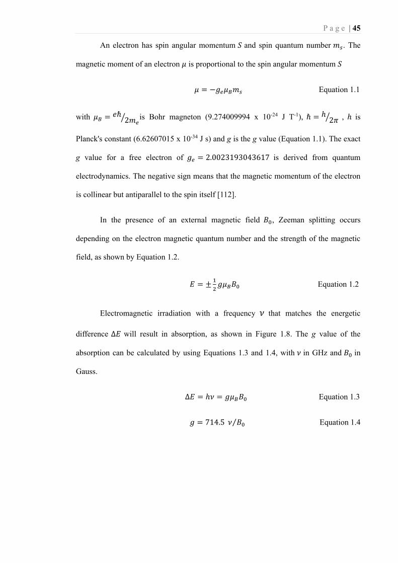
An electron has spin angular momentum 𝑆 and spin quantum number 𝑚𝑠 . The
magnetic moment of an electron 𝜇 is proportional to the spin angular momentum 𝑆
𝜇 = −𝑔𝑒𝜇𝐵𝑚𝑠 Equation 1.1
with 𝜇𝐵 = 𝑒ℏ2𝑚𝑒
⁄ is Bohr magneton (9.274009994 x 10⁻²⁴ J T-1), ℏ = ℎ2𝜋⁄ , ℎ is
Planck's constant (6.62607015 x 10⁻³⁴ J s) and g is the g value (Equation 1.1). The exact
g value for a free electron of 𝑔𝑒 = 2.0023193043617 is derived from quantum
electrodynamics. The negative sign means that the magnetic momentum of the electron
is collinear but antiparallel to the spin itself [112].
In the presence of an external magnetic field 𝐵0 , eeeman splitting occurs
depending on the electron magnetic quantum number and the strength of the magnetic
field, as shown by Equation 1.2.
𝐸 = ±1
2𝑔𝜇𝐵𝐵0 Equation 1.2
Electromagnetic irradiation with a frequency 𝜈 that matches the energetic
difference ∆𝐸 will result in absorption, as shown in Figure 1.8. The g value of the
absorption can be calculated by using Equations 1.3 and 1.4, with 𝜈 in GHz and 𝐵0 in
Gauss.
∆𝐸 = ℎ𝜈 = 𝑔𝜇𝐵𝐵0 Equation 1.3
𝑔 = 714.5 𝜈 𝐵0⁄ Equation 1.4
Page 47
P a g e | 46
Figure 1.8 Energy levels of an unpaired electron spin in the applied magnetic field.
Resonant energy absorption (Equation 1.3) leads to an electron spin ‘flip’ or transition
resulting in an EPR signal. The signal can be presented in absorption (dotted) or first
derivative (solid) mode. Taken from [112].
EPR uses this electromagnetic absorption principle to detect molecules or atoms
that have unpaired electrons by detecting the changes in the electromagnetic resonance
frequency. The resonance detection can be conducted in two ways; either the
electromagnetic frequency is held constant and the magnetic field is swept or the applied
electromagnetic frequency is varied while the magnetic field is kept constant. EPR
spectroscopy uses the former case because it is easier to vary the magnetic field than to
change the frequency. Field modulation is used to increase the sensitivity of the detection.
The resultant of the modulated signal is its first derivative as shown in Figure 1.8.
Page 48
P a g e | 47
(i) Relaxation
During the EPR transition, an electron in a lower energy state (spin-down) will
absorb the electromagnetic (EM) radiation and move into a higher energy state (spin-up).
To maintain the net energy between two spin energy states, an electron in the higher
energy state will release a phonon ℎ𝜈 to move into a lower energy state. The transition
from a higher into a lower energy state is called relaxation. The rate of the relaxation
process is expressed as relaxation time. Saturation occurs if the relaxation rate is too slow.
These phenomena can be observed when the absorption does not increase, or line
broadening starts to happen.
There are two types of relaxation process; spin-lattice relaxation and spin-spin
relaxation. In spin-lattice relaxation, the energy is released within the lattice as phonons
(vibrational, rotational and translational energy). The spin-lattice relaxation is
characterised by an exponential decay of energy as a function of time. The exponential
time constant or the spin-lattice relaxation time is denoted as 𝑇1 . In the spin-spin
relaxation, the energy exchange between the spins occurs without transfer of energy to
the lattice. The time constant or spin-spin relaxation time is known as 𝑇2. Both spin-lattice
and spin-spin relaxation contribute to the EPR linewidth (Equation 1.5):
Δ𝐼𝑝𝑝 ∝1
𝑇1+
1
𝑇2 Equation 1.5
The linewidth, in general, depends mainly on spin-spin interactions (𝑇1 > 𝑇2). 𝑇2
increases if the spin concentration is decreased which causes the spin-spin distance in the
system to be larger. 𝑇1 is inversely proportional to the absolute temperature (𝑇1 ∝ T−n)
with n depending on the relaxation mechanism. Thus, cooling the sample increases 𝑇1
and may lead to detectable resonances.
Page 49
P a g e | 48
(ii) The g value
The g value of the free electron 𝑔𝑒 = 2.002319 is a fundamental constant. In real
materials, 𝑔 ≠ 𝑔𝑒 because of the orbital angular momentum contribution to the magnetic
moment. This is often discussed as the g shift (Δ𝑔, Equation 1.6). The mixing of spin
angular momentum and orbital angular momentum is called spin-orbit coupling (SOC,
Equation 1.7).
Δ𝑔 = 𝑔 − 𝑔𝑒 Equation 1.6
𝑔 = 𝑔𝑒 −𝑛𝜆𝑎2
Δ𝐸 Equation 1.7
where 𝜆 is the SOC constant (larger for heavier element), 𝑎2 is the covalency parameter
(≤1), and n is the quantum mechanical coefficient.
Organic free-radicals usually have large Δ𝐸 and small 𝜆 . Inconsequent,
hydrocarbon radicals usually have g values ranging from 2.002 – 2.003, N/O based
radicals have g values between 2.003 – 2.006, and S-based radicals give g-values of 2.007
– 2.010. Transition metal ions with small Δ𝐸 and large 𝜆 can have large g shifts. In the
case of transition metals, g values can be < 𝑔𝑒 when the SOC occurs at an empty orbital.
(iii) Lineshape
The g value can be affected by the orientation of the molecule in the magnetic
field because orbitals are oriented in the molecule. In other words, g values can be
anisotropic. In the fluid form, all of this anisotropy is averaged out. However, in the solid
form, the g value can change as the sample is rotated in different directions.
Page 50
P a g e | 49
Each molecule has a unique axis system called the principal axis system. The g
values measured along the axis are called the principal g values and denoted as 𝑔𝑥, 𝑔𝑦
and 𝑔𝑧. The anisotropic interactions lead to powder spectra (Figures 1.9-1.10).
In powder spectra, the anisotropic resonance can appear as isotropic, axial or
rhombic symmetry. Typical axial and rhombic symmetry spectra are presented in Figures
1.9 and 1.10, respectively. The average g-value is known as 𝑔𝑖𝑠𝑜 can be written as shown
in Equation 1.8.
𝑔𝑖𝑠𝑜 =𝑔𝑥+𝑔𝑦+𝑔𝑧
3 Equation 1.8
Figure 1.9 Typical anisotropic axial spectra for 𝑔𝑧 > 𝑔𝑥 = 𝑔𝑦: 1st derivative line (red)
and absorption line (blue). The Figure was made using a simulator provided in
www.eprsimulator.org [114].
Page 51
P a g e | 50
Figure 1.10 Typical rhombic symmetry spectra: 1st derivative line (red) and absorption
line (blue). The Figure was made using a simulator provided in www.eprsimulator.org
[114].
(iv) Hyperfine Interaction
The hyperfine interaction also known as the hyperfine coupling is the interaction
between the electron and the nuclei. The nuclei of the atoms in a molecule or complex
often have magnetic moments, which produce a local magnetic field at the electron. There
are two selection rules in EPR that allow the interaction between electron spin and nuclear
spin. The selection rules are shown in Equation 1.9:
|∆𝑚𝑠| = 1 𝑎𝑛𝑑 ∆𝑚𝑙 = 0 Equation 1.9
Page 52
P a g e | 51
Figure 1.11 Energy level diagram in a fixed magnetic field for a system with S = 12⁄ and
I = 12⁄ , in the highfield approximation, showing the electron eeeman (Ee) and nuclear
eeeman (Ne) levels, and the perturbation arising from the hyperfine interaction (HF).
The two allowed EPR transitions (solid arrows) result in the experimentally observed
resonances labelled EPR I and EPR II (shown in the inset). Adapted from [112].
The energies E1, E2, E3 and E4 are derived from equation 1.10 with E1 (𝑚𝐼 = − 12⁄ )
and E2 (𝑚𝐼 = 12⁄ ) related to 𝑚𝑠 = − 1
2⁄ and E3 (𝑚𝐼 = − 12⁄ ) and E4 (𝑚𝐼 = 1
2⁄ ) related to
𝑚𝑠 = 12⁄ . The equation 1.10 describe the general equation for hyperfine interaction:
𝐸 = 𝑔𝜇𝐵𝐵𝑚𝑠 − 𝑔𝑁𝜇𝑁𝐵𝑚𝐼 + 𝐴𝑚𝑠𝑚𝐼 Equation 1.10
with 𝑔𝑁 is the nuclear g value, 𝜇𝑁 is the nuclear magneton (5.0508 x 10⁻²⁷ J T-1) and A is
the hyperfine coupling constant.
Figure 1.12 shows a system with S =12⁄ and I = 1 2⁄ (i.e. hydrogen, 1H), and the
result is the appearance of two EPR resonances corresponding to a hyperfine with a
coupling constant a. If there is a second nucleus with I = 12⁄ , each of the signals is further
split into a pair resulting in four signals. For n number of nuclei with I = 1 2⁄ , there are 2𝑛
Page 53
P a g e | 52
EPR signals. The number of hyperfine lines follows the general rule 2𝑛𝐼 + 1, where n is
the number of nuclei and I is the nuclear spin.
Figure 1.12 The EPR spectrum of a system with S =12⁄ and I = 1 2⁄ . The Figure was
made using a simulator provided in www.eprsimulator.org [114].
(v) Temperature dependence of magnetic susceptibility
The temperature dependence of magnetic susceptibility (𝜒) is proportional to the
temperature dependence of the double integral of the EPR signal (𝜒𝐸𝑃𝑅). Therefore, the
magnetic susceptibility behaviour of a material can be determined by fitting the
temperature dependence of the EPR signal intensity with the Curie, Curie-Weiss or Pauli
laws. However, Pauli paramagnetism, characterized by a nearly temperature-independent
susceptibility, is mainly observed on materials having conductive electrons i.e. metals and
the susceptibility is proportional to the density of conduction electron states at the Fermi
level (EF) [115].
Materials with paramagnetic behaviour are known to have weak interacting
permanent magnetic moments. As a consequence of negligible exchange interactions
between moments, a true paramagnetic material shows no sign of magnetic ordering down
to the lowest temperatures. The magnetic susceptibility of a paramagnetic material is
Page 54
P a g e | 53
positive and strongly dependent on the temperature and follows the Curie law (Equation
1.11 and Figure 1.13a):
𝜒 = 𝐶T⁄ Equation 1.11
where C is the Curie constant and T is the absolute temperature. The Curie law
dependence in the sample is indicative of the presence of isolated paramagnetic ions,
radicals or atoms in the material. Diamagnetism is the opposite of paramagnetism since
it has negative magnetic susceptibility due to a moving electron charge in a manner
described by Lenz's law of electromagnetism [115]. Materials with diamagnetism
characteristics do not have unpaired electrons and therefore cannot be analysed by using
EPR spectroscopy.
Ferromagnetism is when the magnetic moments align parallel to each other. The
ferromagnetic susceptibility of a material diverges at the Curie temperature (TC). In
principle, at temperatures below TC, a spontaneous magnetization (magnetization in zero
magnetic fields) within one domain occurs. The spontaneous magnetization increases
with decreasing temperature. A block of a ferromagnet contains a number of domains
whose spontaneous magnetizations compensate mutually so that the total bulk
magnetization is zero. At temperatures above TC, the magnetic moments become
disordered as in a paramagnet due to the fact that the thermal energy is greater than the
magnetic interactions. The transition is reversible. At temperatures above TC, the
magnetic susceptibility follows the Curie-Weiss law (Equation 1.12 and Figure 1.13b):
𝜒 = 𝐶
T−𝜃 Equation 1.12
where the Curie-Weiss constant, θ, is positive, has the dimensions of temperature and has
a value usually close to TC.
Page 55
P a g e | 54
Figure 1.13 The temperature dependence of the reciprocal magnetic susceptibility. a)
Curie law behaviour of a paramagnet; b) Curie-Weiss law behaviour of a ferromagnet; c)
Curie-Weiss law behaviour of an antiferromagnet; d) behaviour of a ferrimagnet. Figure
a-b is taken from [116], Figure c-d is taken from [115].
The magnetic moments can align in an antiparallel fashion due to energetically
favourable conditions and this is called antiferromagnetism. Above a temperature called
the Néel temperature (TN), the arrangement of the magnetic moments becomes disordered
and behaves as a paramagnet. Above the Néel temperature, the magnetic susceptibility
follows Curie-Weiss law (Figure 1.13c and Equation 1.11) with the constant θ is negative.
At temperatures below TN, the susceptibility decreases (inverse susceptibility increases).
Antiferromagnets exhibit zero spontaneous magnetization due to pairs of magnetic
moments coupled in an antiparallel manner and mutually compensate.
Ferrimagnetism happens when the antiparallel coupling of magnetic moments do
not mutually compensate. As a consequence, a net spontaneous magnetization is observed
a) b)
c) d)
Page 56
P a g e | 55
at temperatures below the ordering temperature TC. At temperatures well above TC, the
magnetic susceptibility behaviour is paramagnetic and follows the Curie-Weiss law,
usually with a negative value of θ. At a certain temperature interval above TC, the
temperature dependence of the inverse magnetic susceptibility forms a curve as shown in
Figure 1.13d.
(vi) Instrumentation
The main parts of the continuous-wave (CW) EPR instrument are the microwave
bridge, the cavity, the magnet and the console for signal processing. Figure 1.14 shows
the scheme of a CW EPR spectrometer without the console. The electromagnetic radiation
source and the detector are placed in a box called the microwave bridge. The cavity is a
metal box and its function is not only as a sample holder but also helps to amplify weak
signals from the sample. The magnetic field is modulated at high frequency (100 kHz).
As a result of the field modulation and phase-sensitive detection, the spectrum is recorded
as the first derivative of the absorption (Figure 1.8). The sensitivity of measurement
increases at higher frequencies, but the sample volume decreases and the instrument
becomes more difficult to use.
Phase-sensitive detection with magnetic field modulation can increase the
sensitivity by several orders of magnitude. However, care should be taken when choosing
the appropriate modulation amplitude, frequency and time constants. Using too large a
modulation amplitude (larger than the linewidth of the EPR signal) will make the detected
EPR signal broaden and distorted. Although higher modulation amplitudes cause
broadening of the signal, the integrated intensity of the signal continues to increase
linearly with modulation amplitude. In this case, high modulation amplitude could be
applied if the main goal of the experiment is spin quantitation. Time constants can affect
Page 57
P a g e | 56
the noise in the spectrum. The increasing time constant can suppress the noise level. If
the time constant is too long for the scan rate of the magnetic field, the signal may be
distorted or even missed. A slower scan rate must be used if the user wants to use a long
time constant to suppress the noise further.
Figure 1.14 The scheme of a CW EPR spectrometer employing magnetic field
modulation. The Figure is taken from [117].
(vii) Pulsed EPR
Pulsed EPR uses a range of microwave frequencies for set periods of time defined by
pulse sequences. The pulse sequences can be divided into the following steps (Figure
1.15): a) At equilibrium, the average magnetic moment of a group spins of a sample will
be parallel to the magnetic field. b) A 90-degree pulse at resonant frequency radiation is
applied, and spins respond in bulk by tipping into the X-Y plane. c) Due to local
inhomogeneities of magnetic field (variation in the magnetic field at different parts of the
sample and at constant time), as the net magnetic moment precesses, some spins slow
down due to lower local field strength while some speed up due to higher field strength
Page 58
P a g e | 57
and thus make the signal decay [free-induction decay (FID)]. d) A 180-degree pulse is
then applied, and the magnetic moment flips 180 degrees, the slower spins now lead ahead
of the main magnetic moment and the fast ones trail behind (rephasing spins). e)
Progressively, the fast and the slow magnetic moments eventually catch-up with one
another resulting in a refocusing spin or “spin echo”. The intensity of the echo is affected
by the time between the two pulses (tau) and can be monitored by integration in pulsed
EPR experiments. Therefore, the spin-echo decay can be observed by recording the
changes in the size of the echo for different values of tau resulting in an exponential decay
diagram, which describes the spin-spin relaxation time (T2).
Figure 1.15 Illustration of the magnetization vector at characteristic positions in the
typical 2-pulse sequence. Adapted from [118].
(viii) Inversion recovery
Inversion recovery with echo detection can be used to measure spin-lattice
relaxation time ( 𝑇1 ). Three-pulse inversion recovery uses a 𝜋 − 𝑡 − 𝜋 2 −⁄ 𝜏 − 𝜋
sequence to generate an echo at tau after the last pulse. A π pulse inverts the magnetization
and the echo integration is detected as the delay pulse (t) is increased. In order to extract
the signal from noise, the echo needs to be averaged by repeat scans.
Page 59
P a g e | 58
(ix) Electron spin echo envelope modulation
Electron spin echo envelope modulation (ESEEM) can be used to detect weak
hyperfine couplings. Two-pulse ESEEM uses a simple 𝜋 2⁄ − 𝜏 − 𝜋 pulse sequence to
generate a primary echo detected at time τ after the second pulse. The issues with the two-
pulse ESEEM are: a) unresolved Fourier transformation of the low-frequency modulation
time trace due to the typically short phase memory time (TM) which leads to unresolved
spectra. b) Spectrometer dead-time (𝜏𝑑, ~100 ns at X-band frequency) which leads to
distortions or artefacts in the resulting frequency-domain spectrum [112]. Some of the
limitations of two-pulse ESEEM can be overcome by three-pulse ESEEM which uses
𝜋 2⁄ − 𝜏 − 𝜋 2 − 𝑡 − 𝜋 2⁄⁄ as a pulse sequence. The three-pulse ESEEM sequence
generates a stimulated echo observed at time τ after the third pulse. The experimental time
trace of an electron coupled to a single nuclear spin equation includes TM and the nuclear
phase memory time (TM(N)), which is longer than TM, leading to narrow lines in the
frequency-domain spectrum and therefore increases the spectral resolution. However, the
three-pulse ESEEM is still affected by blind-spot behaviour [112].
(x) Hyperfine sublevel correlation
The hyperfine sublevel correlation (HYSCORE) spectroscopy is a four-pulse
microwave sequence in which a mixing π pulse is inserted between the second and the
third 𝜋 2⁄ pulse of the three-pulse ESEEM experiment; the total sequence
becomes 𝜋 2⁄ − 𝜏 − 𝜋 2⁄ − 𝑡1 − 𝜋 − 𝑡2 − 𝜋 2⁄ . The two pulse delays 𝑡1 and 𝑡2 are
varied independently to produce a two-dimensional (2D) time delay array. The Fourier
transformation of the modulated time decay data for both 𝑡1 and 𝑡2 is presented in a 2D
frequency-domain spectrum with 𝑣1and 𝑣2 as axes. In HYSCORE, the frequencies from
weakly-coupled nuclei appear as cross-peaks in the (+,+) quadrant, whereas strongly-
Page 60
P a g e | 59
coupled nuclei are observed in the (-,+) quadrant. For disordered systems with broad
ESEEM features, the correlation peaks broaden into ridges as illustrated in Figure 1.16.
Figure 1.16 a) 2D HYSCORE spectrum where full squares ■ represent cross-peaks from
weakly coupled nuclei in the (+,+) quadrant, and full circles ● represent cross-peaks from
strongly coupled nuclei in the (-,+) quadrant. 𝑣𝐿 is the Larmor frequency for the nucleus
of interest, A is the hyperfine coupling, 𝑣𝛼(= 𝜔12) and 𝑣𝛽(= 𝜔34); b) (+,+) quadrant for
the powder HYSCORE pattern for an S = I = 1 2⁄ spin system with an axial hyperfine
tensor. The Figure is taken from [112].
1.4.2 State-of-the-art of EPR in graphene
A selection of published papers on CW EPR of graphene materials has been
summarized in Table 1. Although some results have been presented, the field is still open
for discussion as different types of graphene have been investigated (LPE, CVD grown
etc.) with very little information on the type of graphene analysed (thickness, lateral size,
defects etc.). Therefore, a more detailed study, with well-characterized samples, is
necessary. EPR spectroscopy from a single layer of graphene may give a very weak signal
and limited information as the conduction electron spins which affected by the Fermi
level (EF) position would not be resolved. The EPR spectroscopy from a stack of graphene
Page 61
P a g e | 60
sample is stronger and may be affected by the conduction electron spins due to interlayer
interaction affecting the EF position causing a more complicated EPR spectroscopy.
Year Type of Graphene EPR result References
2009
Mechanically exfoliated graphene
on Kapton scotch-tape;
Dominated by multilayer
graphene
g value 2.0034; single
Lorentzian lineshape; Curie
behaviour; linewidth broadening
at low temperature
[14]
2011
Commercial graphene deposited
on amorphous SiO2 under
vacuum; Produced by substrate-
free gas-phase synthesis
g value 2.00245 ± 0.00005;
single isotropic Lorentzian
lineshape; Curie-Weiss
behaviour (antiferromagnetic)
[15]
2012 Synthesized graphene nanoribbon
g value 2.0032; isotropic non-
Lorentzian lineshape; Curie
behaviour
[36]
2012
Synthesized graphene
nanoribbons; Split (GNRs) and
oxidative unzipped
ribbon(CCGNRs)
g value 2.0025 (GNRs) and
2.0032 (CCGNRs);
ferromagnetic (GNRs); the
number of spin GNRs is 2
orders of magnitude higher than
CCGNRs
[16]
2013
Commercial graphene deposited
on SiO2
g value 2.00245 ± 0.00005;
antiferromagnetic; linewidth
decreased linearly with
temperature
[18]
2014 Synthesized graphene multilayer
g value 2.0044; single isotropic
Lorentzian lineshape; linewidth
broadening at low temperature;
[20]
2014 CVD graphene deposited on SiO2
g value ~2.002; a mixture of
Gaussian and Lorentzian
lineshape with small
anisotropic; antiferromagnetic
[19]
2016 CVD graphene in a transistor
device
g value ~2.0033-2.0036 (with
applied voltage); a mixture of
Gaussian and Lorentzian; Pauli
paramagnetism
[119]
2016 Annealed reduced graphene
oxides
g value ~2.004 (annealed at
1000 oC); Isotropic single EPR
line;
[120]
2017 Reduced graphene oxides Three Lorentzian components
with g value 2.0000-2.0031 [121]
Table 1 CW EPR studies on graphene materials.
Page 62
P a g e | 61
From a theoretical point of view, the origin of magnetism in graphene may come
from vacancies defects [122], zig-zag edge states of graphene [28, 123], absorption of
adatoms [124, 125]. In regard to zig-zag edges, electron spins would be strongly coupled
in parallel with each other through strong ferromagnetic interactions. However,
Kunstmann et al. revealed that magnetic edge states might not exist in real systems and
showed that there are at least three very natural mechanisms which dramatically reduce
the effect of edge states or even totally eliminate them. The three mechanisms are edge
reconstruction, edge passivation, and edge closure [28].
In the case of graphene exfoliation, the exfoliation method can significantly affect
the composition of the samples. As consequences, each sample can have different EPR
behaviour. A temperature-dependent study on mechanically exfoliated graphene revealed
that the g-value is slightly decreased below 70 K, and the linewidth begins to broaden
below 70 K (Figure 1.17a). The former is due to strong coupling of the defects to the
conduction electrons at a lower temperature, while the latter is due to the motional
broadening of the dipolar linewidth of localized spins. The graphene sample was reported
to consist of mono-layer and ultra-thin graphite [14].
a)
Page 63
P a g e | 62
Figure 1.17 Temperature dependence of the EPR linewidth for mechanically exfoliated
graphene (a) [14] and LPE graphene (b) [15].
A study on LPE graphene has shown different temperature-dependent behaviour.
Figure 1.17b shows the linewidth narrowed as the temperature decreases. The authors did
not discuss further the linewidth changes and they postulated that the source of localised
states in their sample was due to vacancies created from vacuum treatment [15].
In another study on LPE graphene, the authors reported that they were able to
observe an EPR signal after the sample was put inside a high vacuum for 60 hours. The
resonance situated at ~210 mT was thought to be a ferromagnetic resonance (FMR) line.
The resonance centre for the FMR signal was shifted to a lower value at low temperature,
as shown in Figure 1.18, due to the presence of the local magnetic field [37].
b)
Page 64
P a g e | 63
Figure 1.18 a) Temperature dependence of the electron spin resonance (ESR) signal from
LPE graphene. b) Temperature dependence of normalized ESR susceptibility measured
after the annealing treatment showing a weaker signal which assigned to the conducting
electrons. The solid line corresponds to the Curie law. The spectrum in the inset was
recorded at 100 K with 64 accumulations. The Figure is taken from [37].
Tadyszak et al. assigned the signal shown in Figure 1.18b to itinerant spins on the
basis of the Pauli type temperature dependence of the ESR susceptibility. Further, the
weak temperature dependence was thought due to the interactions with the localized states
on the zigzag edges [37].
Itinerant and localised electrons below 50 K on multilayer graphene have been
detected by using multi-frequency (9.4 - 420 GHz) EPR [20, 126]. At 315 GHz and below
40 K the single Lorentzian line started to diminish into a powder spectrum with small g-
a)
b)
Page 65
P a g e | 64
value anisotropy. The anisotropic powder spectrum is formed completely at 2 K with
𝑔𝑥𝑥 = 2.00441, 𝑔𝑦𝑦 = 2.00452 and 𝑔𝑧𝑧 = 2.00431. The isotropic conduction electron
spin, resonant with 𝑔𝐶𝐸𝑆𝑅 = 2.00434, was also observed [126]. The temperature
dependence of the line-width exhibited an anomaly below 70 K (Figure 1.19). They
attributed the anomaly to temperature-induced decoupling of the localised and conduction
electrons [20].
Figure 1.19 Temperature dependence of the linewidth from multilayer graphene. The
inset shows the temperature independence of the g-value. The Figure is taken from [20].
In the terms of EPR lineshape, Tampieri et al. (2014) indicated that the electron
interaction of graphene and graphite samples can be categorized into three types of
situations: (a) non-interacting localized electrons, like in radicals, with small hyperfine
(electron-nuclear) interactions, exhibiting a Gaussian lineshape, (b) electrons localized or
delocalized in narrow regions, with strong electron-electron interaction, exhibiting a
Lorentzian lineshape, and (c) mobile electrons in conductive particles with dimensions
larger than the microwave penetration depth (skin depth), exhibiting a Dysonian lineshape
and normally having low intensity [21].
Page 66
P a g e | 65
Uniaxial g-value anisotropy lineshape was observed from graphene samples
prepared by three different exfoliation routes [127]. The exfoliation routes were
sonicating, shear mixing and stirring (Figure 1.20).
Figure 1.20 EPR spectra of (a) SGN18 graphite powder, (b) ultrasounded, (c) shear mixed,
and (d) stirred few-layer graphene. The inset shows the uniaxial g-value simulated EPR
lineshape for the stirrer prepared sample. The Figure is taken from [127].
Figure 1.20 shows graphene samples which contain two EPR resonances with two
g-values that come from the two crystallite directions (𝐵0 ∥ 𝑐 − 𝑎𝑥𝑖𝑠 𝑎𝑛𝑑 𝐵0 ⊥ 𝑐 −
Page 67
P a g e | 66
𝑎𝑥𝑖𝑠). The c-axis is perpendicular to the graphene sheets. Their graphene samples are
dominated by few-layer graphene with the g-value between the free electron and the
graphite powder. The SGN18 graphite powder displays a broad line of 12.2 mT and g-
value at 2.0148. Ultrasounded few-layer graphene gave a Lorentzian line of 1.1 mT
linewidth at g = 2.0059, while the shear mixed presented a 1.4 mT linewidth at g = 2.0082.
The stirred sample has a uniaxial anisotropic signal with a width of 1.2 mT at g = 2.0094.
The broad line components for the SGN18 graphite sample was thought due to conduction
electrons present in graphite. The narrow anisotropic lines are associated with defects and
dangling bonds in all cases [127].
Graphite, however, is different than graphene. Graphite, either natural graphite or
synthetic graphite such as highly oriented pyrolytic graphite (HOPG), has a paramagnetic
signal and the EPR lineshape may depend on its crystal size [127-131]. Natural graphite
usually has relatively large crystals and Dysonian lineshapes. The Dysonian lineshape
associated with conduction electron typically appears for crystals with a size of more than
3 μm (skin depth) [129, 132, 133]. Nano graphite, however, showed different EPR spectra.
The typical Dysonian line was not present in the sample. The spectrum was a single and
narrow EPR line that could be simulated with a single Lorentzian lineshape with g-value
at 2.0035 [128].
Page 68
P a g e | 67
1.5 Raman spectroscopy
1.5.1 Raman basic principles
The Raman effect was discovered in 1928 by Sir Chandrasekhra Venkata Raman
[134]. Light is an electromagnetic wave quantised as a photon, with energy ∆𝐸 (Equation
1.12).
Δ𝐸 = ℎ𝜈 Equation 1.13
with ℎ is the Planck constant (6.626 𝑥 10−34 𝐽𝑠) and 𝜈 is the wave frequency.
Matter interacts with the electromagnetic wave in different ways, depending on
the wave frequency or the wavelength. X-ray light will be diffracted by atomic lattice;
light in the UV-Visible spectrum will cause electron excitation - molecules with
conjugated π systems tends to fluorescence under UV [135-137]; light in the IR-Visible
region will cause excitations of vibrational and rotational levels of molecules and crystals
[138, 139]; microwaves will cause rotational levels of gaseous molecules [139].
Incident light is scattered elastically (re-scattered with the same frequency as the
incident light) from atoms of the material. The light interacts with the molecule and
distorts (polarize) the cloud of electrons around the nuclei to form a short-lived state
called a virtual state. This state is not stable and the photon is quickly re-radiated with the
same frequency as the incident radiation while the cloud of electrons drops back down to
the original state [140]. This effect is known as Rayleigh scattering.
However, a small portion of the incident light is also scattered inelastically (re-
scattered with a different frequency than the incident light). This happens when the
nuclear motion is induced during the scattering process causing the energy transfer either
from the incident photon to the molecule or from the molecule to the scattered photon
Page 69
P a g e | 68
[140]. The energy of the scattered photon is different from the incident photon by one
vibrational unit. This effect is called Raman scattering. Raman scattering is a weak effect
as it happens once in 106 - 108 incident photons. Figure 1.21 shows the basic processes
which occur for one vibration.
Figure 1.21 Schematic of the Rayleigh and Raman processes. The lowest energy
vibrational state m is shown at the foot with a state one vibrational unit in energy above
it labelled n. Rayleigh scattering also occurs from higher vibrational levels such as n.
Taken from [140]
At room temperature, most molecules, but not all, are present in the lowest energy
vibrational level. The Raman scattering process from the ground vibrational state m leads
to absorption of energy by the molecule and its promotion to the higher energy excited
vibrational state n. This is called Stokes scattering. However, due to thermal energy, some
molecules may be present initially in an excited state as represented by n in Figure 1.21.
Scattering from these states to the ground state m is called anti-Stokes scattering and
involves the transfer of energy from the molecule to the scattered photon. This process is
less probable than the Stokes process. The relative intensity of the anti-Stoke process is
Page 70
P a g e | 69
very weak and depend on the Boltzman population states distribution [140]. At room
temperature, the number of molecules expected to be in an excited vibrational state other
than really low energy states will be small. Thus, a typical Raman spectrum only shows
the Stoke lines. In general, anti-Stokes scattering will become weaker the higher the
energy of the vibration, due to the decreasing population of the excited vibrational states.
However, anti-Stokes scattering will increase relative to Stokes scattering as the
temperature rises [140]. In this report, we will only show the Stokes side of the Raman
spectrum.
1.5.2 Raman spectrum of graphene
Raman spectroscopy is the most used non–destructive method for the
characterization of graphene [62, 141, 142]. The spectrum of graphene shows two main
peaks, called the G and 2D peaks, in the region of 1200-3000 cm-1, Figure 1.22.
Figure 1.22 a) Mechanically exfoliated graphene showing both monolayer and bi-layer
regions. b) Raman spectra of mono and bi-layer graphene. The top and bottom insets
Page 71
P a g e | 70
represent the enlarged 2D bands of regions B and A, respectively. The Figure is taken
from [143].
The G band which lies around ~1580 cm-1 corresponds to the bond stretching of
all pairs of sp2 atoms. The 2D band (~2700 cm-1) is the second-order harmonic (overtone
or higher-order Raman processes) of the D band. The D band (usually lies around ~1350
cm-1) is not visible in the Raman spectrum of defect-free graphene because the D band is
defects-activated. However, in the case of a second-order mode, no defects are required
for its activation. The 2D band is always present, even if the D peak is not visible because
it is an overtone and therefore always satisfies momentum conservation. The 2D peak is
very important because its shape allows identification of graphene. In graphene, the 2D
peak is a single and narrow peak, in contrast to few-layers and graphite, where the 2D
peak has a more complex lineshape [144] as shown in Figure 1.22.
If graphene contains defects, then additional peaks are observed in the Raman
spectrum as shown in Figure 1.23. The D band, at around ~1350 cm-1, is due to the
breathing modes of sp2 atoms and requires a defect for its activation [145, 146]. The D
peak intensity has been related to the amount of disorder [145]. Another defect-activated
peak is the D’ peak, seen at around ~1620 cm-1. Defects are also responsible for the
appearance of the combination mode at around ~2950 cm-1 [147]. This mode is the
combination of the D and D’ phonons and requires a defect for its activation.
Page 72
P a g e | 71
Figure 1.23 Raman spectrum of defective graphene showing the main Raman features
taken with a laser excitation energy of 2.41 eV. The Figure is taken from [148].
The ratio between D and D’ bands is very sensitive to the type of defect according
to previous studies [142, 149, 150]. A ratio 𝐼𝐷 𝐼𝐷′⁄ is maximum ( ≅ 13) for defects
associated with sp3 hybridization, it decreases for vacancy-like defects (≅ 7), reaches a
minimum for boundary-like defects in graphite (≅ 3.5) [150].
In the case of LPE graphene, due to the processing involved in the production of
this type of graphene, the Raman spectrum is different from the typical Raman spectrum
shown in Figure 1.22 (where graphene was produced by mechanical exfoliation). The
typical Raman spectrum of LPE graphene is shown in Figure 1.24.
Page 73
P a g e | 72
Figure 1.24 Typical Raman spectra of liquid-phase exfoliated graphene recorded with
514 nm laser. The Figure is taken from [62].
The Raman spectrum of LPE graphene shows a D peak, which is activated by the
edges of the graphene sheets having the size of the sheets comparable to that of the laser
spot [141]. Furthermore, the Raman spectrum of LPE graphene shows a more complex
2D lineshape [63, 151] because of the LPE processing [62]. Some of the sheets in LPE
graphene will re-stack in random stacking and result in complex 2D peak lineshapes as
observed in a twisted bilayer [152, 153].
A simple method to estimate the amount of graphene in a graphene dispersion
produced by LPE was proposed [62, 151, 154, 155]. The protocol is based on a statistical
analysis of the 2D peak lineshape. In general, the single-layer graphene (SLG), few-layer
graphene (FLG, restacked or retaining AB stacking) and graphitic material (> 7 layers
with AB stacking) can be distinguished by evaluating the coefficient of determination R2
of Lorentzian lineshape fitting. Graphite is easily identified by its two peak shape. The
single-layer can be identified by the narrow symmetrical 2D lineshape with 𝑅2 ≥ 0.987.
Page 74
P a g e | 73
The restacked FLG is identified when the 2D shape shows a single asymmetric peak with
0.987 > 𝑅2 ≥ 0.985. The 2D shape of FLG (retaining AB stacking) can be distinguished
by the single 2D peak with 𝑅2 < 0.985. The spectra obtained are fitted with a Lorentzian
line to determine 𝐼𝐷
𝐼𝐺⁄ and 𝑅2 (coefficient of determination). Previous results showed
that the qualitative Raman analysis obtained following this protocol was in agreement
with the results obtained by transmission electron microscopy (TEM) [151, 154, 155].
The procedure requires measurement of 20-50 isolated flakes, drop cast on a silicon
substrate. Graphite residuals are excluded from the analysis. The flake must look like a
small and transparent (almost invisible) individual dot.
Page 75
P a g e | 74
1.6 Aims and objectives
The thesis aim is to investigate the paramagnetism of graphene and its derivative
(i.e. fluorinated graphene) by using EPR spectroscopy. The application of EPR
spectroscopy in graphene characterization is less known compared to Raman
spectroscopy. There are only a few published papers about EPR on graphene (Section
1.4.2). Furthermore, most of the EPR studies have been conducted on poorly
characterized graphene. However, it is of vital importance to correlate the properties of
the materials with the EPR signal in order to get insights about the magnetic properties of
graphene which are crucial for realising its many proposed applications. The objectives
of this project are the following:
1) To study the temperature dependence of the EPR spectrum of well-
characterized graphene and its derivatives
2) To study the EPR signal decay over time of graphene samples.
3) To observe how defects in graphene samples affect the EPR spectrum.
The graphene samples will be made from several production methods (i.e. liquid-
phase exfoliation, electrochemical exfoliation, and graphene made from reduced
graphene oxide), which will allow comparison.
Page 76
P a g e | 75
2. CHAPTER TWO
Electron Paramagnetic Resonance Study of Graphene
Laminates
2.0 Introduction
Since the first successful isolation of graphene in 2004 at the University of
Manchester [2] many properties have been identified and it is expected to be exploited in
a wide range of applications [5, 38, 156]. Studies on the electron spin that can generate a
magnetic moment in graphene attract a lot of attention due to the possibility of using
graphene in advanced and niche applications [24, 157-159]. Moreover, graphene also
shows high electron mobility [9] and shows some intrinsic spin-orbit interaction and
hyperfine interaction of the electron spins with carbon nuclei [160] that make it attractive
for spintronic devices.
Magnetic properties in graphene are often associated with the interaction of the
localized and itinerant conduction electron spins [14-21]. Paramagnetism in graphene
may arise from active defects such as in-plane vacancy defects/dangling bonds and non-
bonding edge defects [22-24]. Interestingly according to theoretical studies, edge states
consisting of nonbonding π-electrons located at the edge region [11] are often discussed
due to their contribution to the paramagnetic activities of graphene [31-33]. Most of the
studies presented focused on the interaction of magnetic moments within a single layer
of graphene, while only a few discussed the interaction of magnetic moments within
multilayer stacked graphene [161-163]. Other theoretical studies show that magnetic
states existing in the active edge defects might not survive in normal conditions due to
Page 77
P a g e | 76
self-reconstruction and passivation by other atoms/molecules [28-30]. An active defect
can be introduced by removing a carbon atom via irradiation [19, 164], sonication [64,
65, 70, 71] or by attaching a stable radical [165]. The latter method is appealing because
the method allows for controlling the defect setting but was also inefficient as the method
used a bottom-up approach.
The sonication method also known as liquid-phase exfoliation (LPE) is a well-
known method to produce high-quality graphene in large quantity. However, to identify
the area of the defect induced by sonication remains a challenge [64, 65, 70, 71]. Active
defects are often described as a preliminary condition for the existence of magnetic order
[25-27], although the recent results on the existence of magnetic ordering in graphene
[35, 166-168] raise some doubt because the observed magnetization of graphene was
considered small (0.1-1 emu/g) [22, 35, 168]. Recently, Slota et al. [165] have
demonstrated a method to inject spin density into the edge states of stable graphene
nanoribbons (GNRs) by attachment of nitronyl nitroxide (NIT) radicals. The results
indicated the presence of delocalized spin states at the GNRs edges. The delocalized spins
at the GNRs edges were clearly visible at high-frequency electron paramagnetic
resonance (EPR) bands [Q (~34 GHz) and W (~94 GHz)], while at X (~9.8 GHz) band,
the edge spin signal overlapped with the NIT radicals signal.
A point of reference in the EPR study of graphitic materials is the seminal work
of Wagoner [169] in a study of perfect single crystals of graphite. The EPR line shape
was of the Dysonian form which is characteristic of the presence of conduction electron
spins in metals. The peak heights A/B ratio was 3.0 where A was the distance of the peak
from the baseline in the positive intensity direction and B was the distance of the peak
from the baseline in the negative intensity direction. It was found that the g shift (g factor
minus the free-electron value) and the linewidth are strongly anisotropic. When the
magnetic field was parallel to the graphene planes the g value had a minimum value and
Page 78
P a g e | 77
was 2.0026; a value slightly higher than the free electron value due to small spin-orbit
coupling with carbon atoms. A strong g shift was measured when the field was
perpendicular to the planes giving a value of 2.05 at room temperature. This was most
often defined in the literature as g = 2.05 and g = 2.0026, the c-axis of the crystal being
perpendicular to the carbon planes. The value anisotropy increased with decreasing
temperature with g = 2.127 at 77 K while g remained constant. The magnitude of the
anisotropy of g depends strongly on temperature and on the position of the Fermi level
with respect to the band edge. An increase of temperature was thought to shift the
population of states from close to the band edge to those further away which have smaller
g shifts [169]. The full theoretical distribution of these observations is complex [170] and
a good summary can be found in the work of Beuneu et al [171].
The magnetic properties of different types of graphene samples, often with very
different properties, have been experimentally investigated [16, 19-22, 28, 34-37], making
it difficult to compare the results. The EPR spectroscopy of graphitic materials has shown
large variations in g values [19, 20, 121], line widths [14, 15, 18, 20] and intensities [37,
127] which was not surprising as the resonance phenomena was very complex depending
on the mobility of the charge carriers and its interplay with the spin-lattice relaxation
time. The dimensions, interlayer interactions, defects, and disorder were all important
factors in governing the electron mobility in each crystal and thereby influencing the EPR
signal.
In this study, graphene flakes were produced using liquid-phase exfoliation [61]
and made into laminates. Defects induced paramagnetism on the flakes were assumed to
be a mixture of edge defects [64, 65] and basal plane defects [70, 71]. The linewidth and
magnetic susceptibility were analyzed in the range 10-295 K by using continuous-wave
EPR (CW EPR) at two sample orientations with respect to the magnetic field.
Page 79
P a g e | 78
2.1 Sample Preparation
2.1.1 Liquid phase exfoliation graphene laminate
Graphene dispersions were prepared by following a liquid-phase exfoliation
method reported in previous work [61] with modifications. In detail, 3 mg/ml of graphite
(Graphexel Ltd.) was added into 5 ml of N-methyl-2-pyrrolidone (NMP) (Sigma-
Aldrich). The mixtures were bubbled with nitrogen for 1 minute and then sonicated for 6
days in a bath sonicator (Hilsonic, 40 Hz and 600 W). The graphene dispersion (see
Appendix A, Figure A1a) was obtained after centrifugation at 4000 rpm (1180 g) for 60
minutes to remove the unexfoliated flakes. The obtained supernatant liquids (graphene
dispersion) were put inside a sealed glass bottle and then stored in the fridge for later use.
The graphene laminates (Figure A1b) were prepared by filtering the graphene dispersion
using a durapore membrane (from Merck Millipore) which is EPR silent (Figure A10).
Acetone (Sigma-Aldrich) was added into the graphene dispersion before filtrating to
flocculate the graphene flakes. Three different graphene laminates were prepared by
filtering a certain amount of graphene dispersion onto a filter membrane. The filtration
was repeated until the solution was clear. Each sample was prepared on a filter membrane
with an area of around ~ 1.77 cm2 (diameter ~ 1.5 cm) (Figure A1b). The three graphene
laminates were 0.113 mg/cm2, 0.566 mg/cm2 and 1.132 mg/cm2. The increasing amounts
of graphene deposited onto the filter membrane caused the thickness of the graphene
laminates to increase.
2.1.2 Graphite
A graphite flake (Graphexel Ltd.) was attached to the inside of the EPR tube by
using scotch tape. The scotch tape was EPR silent (Appendix Figure A10). The sample
Page 80
P a g e | 79
was then cut into 2 x 250 mm2 (W x L) pieces. The graphite plane was parallel with the
scotch tape plane.
2.1.3 Electron paramagnetic resonance
The laminates samples for EPR of each thickness type were prepared by cutting
the membranes to ± 2 mm wide, and stacked into ± 11 layers and put into Suprasil EPR
tubes. Around eleven layers were needed to strengthen the signal, so that the EPR
lineshape could easily be observed at room temperature because one layer of graphene
laminate of the same concentration gave a significantly weaker signal (Figure A4). The
spin concentration of the graphene laminate was calculated by using 2,2-diphenyl-1-
picrylhydrazyl (DPPH) as a standard. DPPH is known to have a g value of 2.0036. All
EPR measurements were taken using 2 mW, 1 G modulation amplitude, 10 scans, 40.96
ms time constant and conversion time, under non-saturating conditions. During the
experiments, the graphene laminates were rotated to produce two different orientations.
The z-axis of the samples was positioned 90o (𝐻⊥) and 0o (𝐻∥) with respect to the magnetic
field (H) (see Figure A2). The EPR measurements were performed on a Bruker EMX X
band (~9.4 GHz) spectrometer equipped with a Bruker cryostat and an Oxford
Instruments Cryospares temperature controller.
Pulsed EPR was performed on a Bruker pulsed ELEXSYS E580 (9.7 GHz)
spectrometer equipped with a cryostat and an Oxford Instruments Cryospares temperature
controller. The measurement was carried out at the 𝐻⊥ orientation using ~3480 G centre
field, ~9.7 GHz frequency with pulse lengths of 16 ns for π/2 and 32 ns for π and pulse
delays of t = 300 and τ = 180 ns. The ESEEM experiment used a step size of 16 ns. The
equation to fit the inversion recovery traces to extract T1 was:
𝑦 = 𝑦0 + 𝐴1 ∗ exp (− 𝑥 𝑡1) + 𝐴2⁄ ∗ exp (− 𝑥 𝑡2⁄ ) Equation 2.1
Page 81
P a g e | 80
𝜏1 = 𝑡1 ∗ 𝑙𝑛(2) Equation 2.2
𝜏2 = 𝑡2 ∗ 𝑙𝑛(2) Equation 2.3
where the fast component was attributed to spectral diffusion (any process that takes spins
resonance [172]) and ignored. The equation to extract T2 value was:
𝑦 = 𝐴1 ∗ exp(− 𝑥 𝑡⁄ ) + 𝐴2 ∗ 𝑥 + 𝐴3 Equation 2.4
𝜏 = 𝑡 ∗ ln (2) Equation 2.5
2.1.4 UV-Vis spectroscopy
The concentration of graphene dispersion was determined by using a Perkin-
Elmer l-900 UV-Vis-NIR spectrometer. The UV spectrum of graphene dispersion tends
to be featureless in the visible-IR region. A Beer-Lambert equation with an absorption
coefficient of 2460 L g−1m−1 was used to calculate the concentration at 660 nm
absorption [61].
2.1.5 Atomic Force Microscopy (AFM)
The average graphene flakes size and shape were analyzed by using a Bruker
Multimode 8 atomic force microscopy (AFM). AFM samples were prepared through
drop-casting the diluted graphene dispersion onto the surface of silicon dioxide. 100
flakes were selected to determine the size distribution. The AFM results were supplied
by Tong Jincheng, School of Chemistry, University of Manchester.
Page 82
P a g e | 81
2.1.6 Raman spectroscopy
A Renishaw Invia Raman spectrometer was used to determine the quality of the
graphene dispersion. The sample for Raman measurements was prepared by drop-casting
the diluted graphene dispersion onto the surface of silicon dioxide. The measurements
were taken by using a 514.5 nm laser excitation with 1 mW laser power, 100X NA0.85
objective lens and 2400 grooves/mm grating.
2.2 Results and Discussion
2.2.1 Graphene flake characterization
The average graphene dispersion concentration was found to be around 0.8 mg/ml.
The graphene flakes were analyzed by Raman spectroscopy using the procedure described
in previous work [62, 154]. Representative Raman spectra are found in Figure A3. Our
qualitative Raman analysis, based on the shape of 2D peak [62] shows that the dispersion
contained ~40 % single-layer graphene, 50 % few-layer graphene (restacked or retaining
AB stacking) and 3 % graphitic material (>10 layers with AB stacking), confirming high
exfoliation efficiency.
The flakes size and shape shown by the AFM are presented in Figure 2.1. The
average flake size is 58 ± 18 nm with random shapes. The topographic height of the flakes
was in the range of 0.7 – 1.6 nm, which is consistent with the existence of thin layers [2,
173, 174], as found by the qualitative Raman analysis.
Page 83
P a g e | 82
(a) (b)
Figure 2.1 Graphene flake shapes (a) and size distribution (b), analyzed by using AFM.
2.2.2 Graphene laminate paramagnetism
The graphene laminates had a spin concentration of 2.9333 x 10¹⁸ spins/g (
1.5864 x 10¹⁷ spins/g) measured at room temperature. The spin concentration was
determined by comparing the double integration of the EPR signal intensity of the
graphene laminates with a known DPPH standard at room temperature [175]. The
measured concentration was two orders of magnitude greater than a previously reported
sample prepared using mechanically exfoliated graphene [14] and the difference is
probably related to the graphene production process. In this study, the relatively long
sonication time may result in a smaller flakes size as well as an increase in the number of
paramagnetic active sites.
20 40 60 80 100 120 1400
10
20
30
40
50
60
Count
Size / nm
Page 84
P a g e | 83
340 344 348 340 344 348In
tens
ity (a
.u.)
Magnetic Field (mT)
a) b)
340 344 348 352 340 344 348 352
Inte
nsity
(a.u
.)
Magnetic Field (mT)
c) d)
Figure 2.2 9.4 GHz EPR spectra of the thick graphene laminate (1.132 mg/cm2) recorded
at 295 K (a and b) and at 10 K (c and d) at two different orientations; a and c represents
𝐻∥; b and d represents 𝐻⊥. The purple line represents the overall simulation result of the
Lorentzian lineshape; the red and blue line represents Lorentzian lineshape of narrow and
broad component, respectively. The simulation was performed by using Easyspin [176].
The EPR lineshape of the graphene laminates at room temperature was best fitted
using Lorentzian lineshapes (Figure 2.2) indicative of homogeneous contributions to the
linewidth and has been attributed to a strong electron-electron interaction, localized or
delocalized [21]. A composite linewidth was observed for the 𝐻⊥ orientation at room
temperature, which could be simulated with overlapping narrow and broad components.
The A/B ratios were both ~1 for the narrow and broad components at both orientations.
The 𝐻∥ orientation at room temperature also showed two separate EPR signals which
represent a narrow and broad component individually. The intensity of the narrow
a
)
b
)
c
)
d
)
Page 85
P a g e | 84
component was stronger at 𝐻⊥ orientation. The linewidth narrowed at 10 K for both
orientations and could be simulated with one component. The changes in the spectra were
further understood by the performance of a more detailed temperature-dependent study
as described in Section 2.2.3.
The linewidth of the narrow component at room temperature and 𝐻∥ orientation
was found to increase from 0.45 ± 0.02 mT (0.113 mg/cm2) to 0.53 ± 0.06 mT (1.132
mg/cm2). The linewidth of the narrow component for the 0.566 mg/cm2 samples was
found to be 0.55 ± 0.18 mT. The change appears to reach a limit and this is probably due
to passivation (see Chapter 4 for further discussion on lineshape evolution due to
passivation) and we choose not to interpret the results in detail. Nevertheless, the
linewidth on thin graphene laminate (0.113 mg/cm2) was narrower compared to the thick
graphene laminate (1.132 mg/cm2). This may arise from an interplay of electrons between
layers. The narrow component is affected by the interaction between localized and
conduction electrons between layers which depend on the degree of disorder (i.e. defects
and stacking disorder). Thus, the disorder in thick graphene laminate may disrupt the
conduction electrons mobility and broaden the linewidth.
The linewidth of the graphene laminate’s broad component was found to increase
as the thickness of the layer increases (Figure 2.3). A linewidth of 2.515 ± 0.211 mT was
found for the 0.113 mg/cm2 samples, while the 0.566 mg/cm2 and 1.132 mg/cm2 samples
displayed linewidths of 2.855 ± 0.267 mT and 4.072 ± 0.295 mT, respectively. Graphite
with an increase of disorder also showed similar broadening [177]. In the current case, an
increase of disorder could be associated with an increase in laminate thickness/graphene
stacking. This, again, could be related to the interlayer electron-electron interaction of the
defective and disordered graphene stacking, which could lead to a change in energy bands
and Fermi level position [169, 171, 178].
Page 86
P a g e | 85
0.0 0.2 0.4 0.6 0.8 1.0 1.2
2.5
3.0
3.5
4.0
4.5
Lin
ew
idth
(m
T)
Graphene laminates (mg/cm2)
Figure 2.3 The room temperature EPR linewidth of graphene laminate’s broad
component at 𝐻∥ orientation on the variation of layer thickness.
2.2.3 Temperature dependence of graphene laminates
The narrow component is considered the main spectral component as it is always
present at a significant intensity. The narrow component had a g value of 2.0031 ± 0.0002.
The deviation of g value from the free-electron value is determined by the contribution
of orbital angular momentum in the electronic states of spins giving rise to resonance.
The g value of the narrow component was temperature-independent and was also in the
range where the mixture of carbon sp2 and sp3-hybridized states has been frequently
observed [128, 179]. This indicates that the EPR signals are originating from carbon-
centred spin states.
The changing of the EPR lineshape as a function of temperature for the 0.566
mg/cm2 sample is shown in Figure 2.4 and for the other samples in Figures A5-A6. At
room temperature, a broad component was observed at both orientations. As the
temperature decreased, the broad component’s intensity weakened and shifted downfield
Page 87
P a g e | 86
away from the narrow component and eventually became unobservable around 50 – 75
K. The shifting of the broad component for 𝐻∥ orientation from room temperature to 75
K was in the range of 0.8 - 2.6 mT. At 𝐻∥ and room temperature, the broad component
had a g value of 2.0151 ± 0.0006 for the 0.113 mg/cm2 sample, 2.0172 ± 0.0053 for the
0.566 mg/cm2 sample and 2.0183 ± 0.0031 for the 1.132 mg/cm2 sample.
338 340 342 344 346 348 350 352
10 K
20 K
30 K
40 K
50 K
75 K
100 K
150 K
200 K
250 K
295 K
Inte
nsity (
a.u
.)
Magnetic Field (mT)
Figure 2.4 The EPR spectra of thin graphene laminates (0.566 mg/cm2) as a function of
temperature. The black line represents 𝐻⊥. The red line represents 𝐻∥.
The g value of the broad component and its temperature dependence appeared to
be affected by the thickness of the graphene laminates/stacking of graphene planes. This
characteristic has also been found in graphite [177] with an increasing amount of disorder
in graphite causing an increase of the g value as the temperature is lowered. The
temperature dependence of the g value for graphite and nanographites has also been
Page 88
P a g e | 87
reported to be affected by the mobility of electrons between graphene planes; the g value
increased as the temperature decreases [129, 169].
The intensity of the broad component decreased proportionally with temperature
and disappeared at around 75 - 100 K. To the best of our knowledge, this has not been
observed before in any graphene or graphite experiments. In addition, the temperature
limit at which the broad components started to disappear was found to get lower as the
graphene laminates got thicker. For example, for the thin graphene laminate (0.113
mg/cm2) the broad component disappeared at ~100 K and for the medium thickness
laminate (1.132 mg/cm2) the broad component disappeared at ~ 75 K. Although the broad
component has never been observed and discussed in previous graphene literature, similar
behaviour has been observed in the case of nanographite [129, 180]. They attributed the
broad component to be as the result of itinerant conduction electron spins, while the
narrow component was representative of localized electron spins [129, 180]. However,
the appearance of broad components was absent in other nano graphite samples [128].
2.2.4 EPR linewidth of graphene laminates
The interaction between localized and itinerant conduction electron spins can be
observed through changes in the EPR linewidth. The coupling of the localized and
itinerant conduction electron spins can cause the average EPR linewidth to narrow as the
temperature decreases. The narrowing behaviour has been reported on nano graphite [128,
181] and graphene [20, 119]. The EPR linewidth of graphitic materials has also been
found to broaden as the temperature decreases [14, 20, 128, 181]. The broadening
behaviour was thought due to decoupling of the localized and conduction electrons [20].
The narrow component of graphene laminate is affected by coupled and decoupled states
of localized and conduction electrons. Figures 2.5 and 2.6 show plots of the EPR
Page 89
P a g e | 88
linewidth of the narrow component against temperature for different graphene laminates
thickness and orientation. Error bars arise from the average of three samples. The
linewidth from 100 K – 10 K for 0.113 mg/cm2 samples for both sample orientations
showed only a slight narrowing while the linewidths for 0.566 mg/cm2 samples practically
remains unchanged (Figures 2.5 and A7). However, the low-temperature EPR linewidth
broadening can be observed in the thicker graphene laminate (1.132 mg/cm2) samples at
the 𝐻∥ orientation (Figure 2.6). Interestingly, this result suggests that the coupling and
decoupling of localized and itinerant conduction electron spins observed at 𝐻∥ orientation
might involve out-of-plane inter-graphene layers interactions. The out-of-plane interlayer
magnetic interactions arising from the disorder are much stronger in the thick graphene
laminates (high number of graphene layers stacked) with high localized spin
concentration leading to a change in the energy bands and shifting of the Fermi level [171,
177]. In addition, the linewidth may also be affected by spin-lattice relaxation [181].
0 50 100 150 200 250 300
0.32
0.36
0.40
0.44
0.48
0.52
Lin
ew
idth
(m
T)
Temperature (K)
a)
0 50 100 150 200 250 300
0.4
0.8
1.2
1.6
Lin
ew
idth
(m
T)
Temperature (K)
b)
Figure 2.5 EPR linewidth of the narrow component for the thin graphene laminates
(0.113 mg/cm2) on the variation of temperature. a) Red square represents 𝐻∥. b) Black
square represents 𝐻⊥.
Page 90
P a g e | 89
0 50 100 150 200 250 3000.35
0.40
0.45
0.50
0.55
0.60
0.65
Lin
ew
idth
(m
T)
Temperature (K)
a)
0 50 100 150 200 250 300
0.4
0.8
1.2
1.6
2.0
Lin
ew
idth
(m
T)
Temperature (K)
b)
Figure 2.6 EPR linewidth of the narrow component for the thick graphene laminates
(1.132 mg/cm2) on the variation of temperature. a) Red square represents 𝐻∥. b) Black
square represents 𝐻⊥.
The linewidths at the 𝐻⊥ orientation from 300 – 150 K was affected by the
presence of the broad component overlapping with the narrow component due to the
anisotropic behaviour of the broad component. Thus, the EPR peak-peak linewidth was
difficult to measure. Thus, we choose not to interpret the data from 300 – 150 K.
In contrast to the temperature dependence of the linewidth for the narrow
component, the linewidth of the broad component for all samples at 𝐻∥ was seen to
broaden as the temperature decreases. This was observed as the intensity of the broad
component decreased with decreasing temperature. The broadening of the linewidth and
the decreasing of the intensity was possibly due to the limitation of electron mobility as
the temperature decreases and the displacement of Fermi level position [129, 169].
2.2.5 Comparison to graphite
The comparison was made to a single flake of graphite in order to help understand
the lineshape of the graphene laminates and the influence of itinerant conduction
electrons. Figure 2.7 displays the EPR spectra of graphite recorded at different
Page 91
P a g e | 90
temperatures, showing the influence of conduction electrons. The graphite flake showed
Dysonian lineshapes at room temperature with an A B⁄ (∥) ratio of 2.77 and A B⁄ () ratio
of 1.75. Similarities and differences at equivalent temperatures were found in comparison
to the laminates:
i) The resonances at the 𝐻∥ orientation shifted to a lower magnetic field and the intensity
was reduced and finally disappeared.
ii) The resonance along the 𝐻∥ orientation also came into resonance at a much lower
magnetic field.
Figure 2.7 EPR spectra of a graphite flake as a function of temperature. (a) represents
𝐻⊥. (b) represents 𝐻∥. (*) marks a speculate asignment of the broad component at 70 K.
Page 92
P a g e | 91
The g value of the resonances at the 𝐻∥ orientation for the graphite flake was
2.0419 ± 0.0046 while the laminates have g values in the range of 0.0236-0.0268 less than
the graphite (see Section 2.2.3). The magnitude of the g value of graphite at 𝐻∥ orientation
has been reported to depend strongly on temperature and on the position of the Fermi
level with respect to the band edge [169]. Further, the large g-shift in graphite along the
𝐻∥ orientation has been explained due to the change in the energy bands (degeneracy) of
graphite at the zone edge. The g value anisotropy of the graphite is affected by the
stacking of graphene planes and the mobility of electrons between planes [129, 177].
Accordingly, the graphene laminates were prepared by using vacuum filtration and
according to a previous investigation, they consist of numerous graphene flakes which
are randomly stacked [182]. The loss of AB stacking in the graphene laminate may be
explained due to the change in the degeneracy of the energy bands at the zone edge and
increase of electron mobility [183] causing the decrease of the g value [129].
The linewidth of graphite’s resonance along the 𝐻∥ orientation (Figure A8) was
narrower (∆Hpp = 1.29 mT, at room temperature) compared to the laminates (see Section
2.2.4, Figure 2.6). The alignment of the AB Bernal system in the graphite may be
responsible for the narrower EPR linewidth [177]. Chehab et al demonstrated that an
increase of stacking disorder in graphite broadened the linewidth of graphite observed for
𝐻∥ [177]. The linewidth of graphite’s resonance at 𝐻⊥ orientation and at room
temperature was 0.54 mT (Figure A8).
Studying further Figure 2.7, it clearly shows that the EPR intensity of the graphite
flake at both orientations decreased proportionally with temperature whereas the g value
is constant for 𝐻⊥orientation and increases for 𝐻∥ orientation. Figure 2.7b shows that at
𝐻∥, the resonance can be seen to disappear at ~70 K. The spectra clearly show the change
and movement of the signal. This is similar to the observation in the laminates albeit at a
Page 93
P a g e | 92
different temperature range. To the best of our knowledge, this observation has never
been reported before. Previously, Matsubara et al [170] was able to observe the g value
of highly oriented pyrolytic graphite (HOPG), synthetic graphite, down to ~5 K at 𝐻∥.
The g value increased as the temperature decreased and exhibited a peak at 20 K and then
decreased. The EPR intensity was shown to decrease parallel with the temperature down
to 20 K and then increase. The decrease of g value and the increase of EPR intensity after
20 K was thought to arise due to the contribution of localized spins which become
dominant at low temperatures in accordance with the Curie law. However, in our graphite
flake sample, although the EPR intensity of the resonance at 𝐻∥ was reduced and even
completely unobservable below 70 K, we did not observe a narrow component associated
with localized spins. This could be because the localized spin concentration in our
graphite was probably too small and may be suppressed by the π character of the Fermi-
energy states and therefore the narrow component was unobservable. Interestingly, the
intensity behaviour measured by double integration of our graphite flake at 𝐻⊥ shows
similar behaviour as observed by Matsubara et al. at 𝐻∥ such that the intensity decreases
and reaches a minimum at around 30 K and then increases (Figure A9).
2.2.6 EPR magnetic susceptibility of graphene laminates
The EPR magnetic susceptibility measurements from 10-70 K of graphene
laminates showed anisotropic Curie-Weis behaviour (Figures 2.8-2.10). The equation
used to fit the Curie-Weis behaviour was:
𝜒𝐸𝑃𝑅 =𝐶
T−𝜃 Equation 2.6
where C is the Curie constant, T is the temperature of the sample and θ is the critical
temperature. Both antiferromagnetism and ferromagnetism were observed in the
Page 94
P a g e | 93
graphene laminate samples as judged by fitting of the Curie-Weis equation to the inverse
susceptibility (using double integration of the whole spectrum) below 75 K. Above 75 K
where the broad component exists, the Pauli contribution tends to be the dominant state
due to the EPR line intensity behaviour being dictated by electron-electron interactions
[181].
The thin graphene laminates (0.113 mg/cm2) showed negligible
antiferromagnetism with θ = -0.2 ± 2.5 K close to zero at 𝐻⊥ (Figure 2.8).
Ferromagnetism was observed at 𝐻∥ with θ = 5.2 ± 2.5 K. As the graphene laminate got
thicker, the Curie-Weis temperature changed. The 0.566 mg/cm2 graphene laminate
sample gave θ = -5.4 ± 2.6 K and 5.9 ± 2.1 K, while the 1.132 mg/cm2 graphene laminate
sample displayed θ = -11.5 ± 2.1 K and 9.2 ± 1.9 K for 𝐻⊥ and 𝐻∥ , respectively (Figures
2.9 and 2.10).
The ferromagnetic interaction coexisting with the antiferromagnetic interaction in
graphene has been reported previously in a study which points out that flake size and the
number of layers in the graphene sample can influence the magnetic properties [184]. In
the present work, since the size of the flakes of the three graphene laminates was assumed
to be similar due to the same production method, it is likely that the thickness/the number
of layers stacked should give the most influence to differences in the magnetic properties.
Indeed, Figures 2.8-2.10 clearly reveal that the occurrence of anti/ferromagnetism and it
can be observed clearly as the laminates thickness increases. The Curie-Weis temperature
moved away from 0 K as the laminates thickness increases. As the graphene laminate
thickness increases, the stacking disorder increases. This variable could also impart the
change of magnetism [27, 161].
Page 95
P a g e | 94
0 10 20 30 40 50 60 70 80
1
2
EP
R-1
(10
-5)
Temperature (K)
1
2
3
(10
-5)
Figure 2.8 Curie-Weis behaviour of thin graphene laminates (0.113 mg/cm2) measured
from 10-75 K. Black dots represents 𝐻⊥, θ = -0.2 ± 2.5 K. Red dots represents 𝐻∥, θ = 5.2
± 2.5 K. Blue line represents the Curie-Weis line.
1
2
3
4
5
0 10 20 30 40 50 60 70 80
0.5
1.0
1.5
(10
-5)
E
PR
-1(1
0-5
)
Temperature (K)
Figure 2.9 Curie-Weis behaviour of thick graphene laminates (0.566 mg/cm2) measured
from 10-75 K. Black dots represents 𝐻⊥, θ = -5.4 ± 2.6 K. Red dots represents 𝐻∥, θ = 5.9
± 2.1 K. Blue line represents the Curie-Weis line.
Page 96
P a g e | 95
0 10 20 30 40 50 60 70 80
2
4
6
8
1
2
3
E
PR
-1(1
0-6
)
Temperature (K)
(10
-5)
Figure 2.10 Curie-Weis behaviour of thick graphene laminates (1.132 mg/cm2) measured
from 10-75 K. Black dots represents 𝐻⊥, θ = -11.5 ± 2.1 K. Red dots represents 𝐻∥, θ =
9.2 ± 1.9 K. Blue line represents the Curie-Weis line.
A study on graphene magnetism reveals that the alignment of the spins in
graphene might depend on the distribution of the spin population within graphene
sublattices and stacking disorder [162]. In addition, the antiferromagnetic behaviour in
graphene has been discussed previously [15, 19]. The exchange interaction between
localized states and conduction electrons might be responsible for such behaviour.
Another theoretical study on stacked graphene, realizing the energy difference between
different stack sequences, predicted that the net magnetic ordering was due to lower total
energy causing stable conditions to allow magnetic moment alignment [163]. Figures 2.8-
2.10 showed that the ferromagnetism in the graphene laminate could be observed at 𝐻∥,
while the antiferromagnetism appeared at 𝐻⊥ . The results suggest energetically
favourable orientation-dependence of the interlayer interactions of localized spins and
indirectly conduction electron spins. According to theoretical studies, the spins at zig-zag
edges (edge states) are strongly polarized and are coupled through ferromagnetic
Page 97
P a g e | 96
interactions [16, 37]. However, the discussion of the ferromagnetic source has to be
limited because of the existence of zig-zag edges within the graphene laminates cannot
be quantitatively verified. The percentage of the zig-zag edges within the samples can be
determined statistically by observing several numbers of individual flakes. However, the
method is time-consuming and would require high-resolution AFM or Transmission
Electron Microscopy (TEM).
2.2.7 Relaxation times and nuclear resonances of the graphene laminates
Pulsed EPR experiments were used to measure relaxation rates of the graphene
laminates (Figures 2.11). The spin-spin relaxation time (T2) and spin-lattice relaxation
time (T1) of the graphene laminates were observed over a temperature range of 10 – 70 K
(Figure 2.11) which showed a weak temperature dependence. The T2 was practically
unchanged and fluctuated between 0.9 – 1.2 µs over the temperature measurement.
Similarly, the T1 values showed little variation with a weak trend for decreasing values at
a lower temperature. For example, T1 varied from ~20 µs at 10 K to ~15 µs at 70 K. This
is consistent with relaxation playing only a minor role in the changes of line width.
1.0 1.2 1.4 1.6 1.8
5
6
7
Lo
g(1
/T2 s
-1)
Log(T (K))
a)
1.0 1.2 1.4 1.6 1.8
4
5
6
Lo
g(1
/T1 s
-1)
Log(T (K))
b)
Figure 2.11 The spin-spin relaxation time (T2) (a) and spin-lattice relaxation time (T1) (b)
of a graphene laminate over the temperature range of 10 – 70 K at the 𝐻⊥ orientation.
Page 98
P a g e | 97
Electron spin echo envelope modulation (ESEEM) experiments were performed
to analyse the presence of nuclear-electron spin coupling. Figure 2.12 shows the
identification of nuclear magnetic resonances arising from 13C and possibly for 14N. The
signal to noise (S/N) ratio was low to confirm the 14N resonance, nevertheless, the
detected resonance was possibly from the residual NMP solvent. The magnetic coupling
can be a source of relaxation.
0 2 4 6 8 10 12 14 16 18 20 22 24 26 28 30
0
1
2
3
4
ES
EE
M A
mp
l. x
10
7(a
.u.)
Frequency (MHz)
14N
13C
Figure 2.12 ESEEM spectrum of graphene laminate at 10 K at the 𝐻⊥ orientation.
2.3 Conclusion
The experiments have shown that localized and itinerant conduction electron spins
exist in graphene laminates and their interactions are affected by spin concentration,
temperature, the order of stacking and the magnetic field orientation. Broad and narrow
components were observed in the CW EPR spectra. The broad component of graphene
laminate was affected by the interlayer coupling of localized and itinerant conduction
electron spins. The g value and linewidth of the broad component was affected by electron
Page 99
P a g e | 98
mobility, the laminate’s thickness, disorder, temperature and orientation in the external
magnetic field. The most likely origin of the broad component is from interlayer
interactions of localized and itinerant conduction electrons. The narrow component was
attributed to localized electrons (vacancy defects). The g value of the narrow component
was assigned to carbon centred spins. The linewidth of the narrow component was
affected by the interlayer interaction between localized and itinerant conduction electrons
as well as spin-lattice relaxation. This was particularly observed through the increase of
linewidth at low temperature for the thick graphene laminate revealing the decoupled and
coupled states of the localized-itinerant conduction electron spins with high localized spin
concentration for the narrow component and 𝐻∥ orientation. The ferromagnetic and
antiferromagnetic interactions present in the graphene laminates may be related to
energetically favourable conditions due to interlayer interaction of localized and
indirectly conduction electron spins within the magnetic field orientation.
Page 100
P a g e | 99
3. CHAPTER THREE
Electron Paramagnetic Resonance Study of the
Electrochemical Exfoliation of Graphite in Comparison
to Graphene Laminates Produced Through
Electrochemical Exfoliation, Liquid Phase Exfoliation
and Chemical Reduction of Graphene Oxide
3.0 Introduction
Low-cost mass production of solution-processable and high-quality graphene
remains a major challenge. Several mass production methods have been developed [185].
Chemical vapour deposition (CVD) has been able to produce high-quality graphene films
with large-area [186]. However, production variables such as high-temperature, a
sacrificial metal catalyst, and the multistep transfer onto the desired substrates could
become obstacles to the cost-effective mass-production scale of CVD graphene. Chemical
or thermal reduction of graphene oxide (GO) is a well-known and cost-effective method
for the mass production of graphene but suffers from the use of toxic reducing agents
such as hydrazine or sodium borohydride. Moreover, the reduced graphene oxide (rGO)
produced was found to only partially restore the electronic properties of graphene [187].
Recently, the use of environmentally friendly reducing agents has become an appealing
topic for the generation of rGO [188-190]. Liquid phase exfoliation (LPE) is another
attractive efficient method to produce graphene. Exfoliation can be achieved by
sonicating graphite either in solvents or in surfactant/stabilizer-aqueous media. The
graphene dispersion obtained was a mixture of single and multilayer graphene. Cascade
Page 101
P a g e | 100
centrifugation could maximize the selection to obtain a single layer graphene enriched
dispersion [191].
Electrochemical exfoliation of graphite is a fast and easy top-down method to
produce graphene in large quantities [192-196]. The exfoliation follows either anodic
oxidation or cathodic reduction. Anodic exfoliation is the most commonly used method
due to the relatively low-cost electrolyte solution and fast intercalation process compared
to cathodic exfoliation. The intercalation at the cathode is usually only able to expand the
graphite; sonication was needed to fully exfoliate the graphite [84, 197-199]. However,
the anodic exfoliation approach was not without problems. The graphene produced
through anodic exfoliation method was partially oxidised or functionalised by other
species involved in the process [73]. The anodic exfoliation mechanism has been
explained in Section 1.3.4 and can be summarized as the following: 1) the positively
charge graphite foil anode attracts anions (negative ions), 2) oxidation of graphene,
intercalation of graphene layers by negative ions, and the formation of gaseous species,
3) expansion and exfoliation of graphene layers [76].
Previously, Krivenko et al [200] demonstrated the use of electron paramagnetic
resonance (EPR) spectroscopy, infrared spectroscopy (IR), X-ray photoelectron
spectroscopy (XPS) and scanning electron microscopy (SEM) to analyse the graphene
powder produced by electrochemical exfoliation of graphite rods. The results suggested
that the powder produced through anode exfoliation had a significantly higher number of
defects compared to the powder obtained in the cathode. The present report further
highlights the use of EPR spectroscopy to study the electrochemical exfoliation of
graphite foil. In addition, this Chapter studies the magnetic properties of electrochemical
exfoliated (EC) graphene laminate with comparison to rGO and LPE laminates. The EPR
spectra generated from the laminates were able to separate and characterize the
contribution of the localized and conduction electrons within the samples.
Page 102
P a g e | 101
3.1 Sample Preparation
3.1.1 Liquid Phase Exfoliation
Graphene dispersions and laminates were prepared and characterised using the
methods described in Chapter 2, Section 2.1.1.
3.1.2 Electrochemical Exfoliation
The graphene solution was prepared as followed. The graphite foil (Sigma-
Aldrich) was cut into ± 1.5 (W) x 3 (L) cm2 strips and was used as the electrodes. A 0.5
M solution of K2SO4 (Sigma-Aldrich) in water was used as the electrolyte. The
exfoliation was carried out by applying 10 V at room temperature for 5 minutes. After
exfoliation, the material was collected and washed with deionized water via vacuum
filtration. The filtered material was then dispersed in NMP (100 mL) using ultrasonication
for 30 minutes. The graphene solution was supplied by Khaled Parvez, School of
Chemistry, University of Manchester.
The graphene solution was sonicated for 6 days. The sample was then centrifuged
at 3500 rpm for 20 min. The electrochemical exfoliated (EC) graphene laminate was
prepared by filtering the graphene dispersion using a Durapore membrane. Acetone was
added into the graphene dispersion before filtrating to flocculate the graphene flakes. The
filtration was repeated until the solution was clear. The sample was prepared on a filter
membrane with an area of around ~ 1.77 cm2 (diameter ~ 1.5 cm). The graphene
laminate had 1.132 mg/cm2 of graphene.
To allow the study of the electrochemical exfoliation process, the sample was
prepared using the following procedure. The graphite foil (Sigma-Aldrich) was cut into ±
2.5 (W) x 100 (L) mm2 strips and was used as the electrodes. A 0.5 M solution of K2SO4
Page 103
P a g e | 102
(Sigma-Aldrich) in water was used as the electrolyte. The exfoliation carried out by
applying 10 V at room temperature for 30 seconds. The electrodes were then washed by
using deionised water followed by an acetone wash and then dried at room temperature.
Thereafter, the electrodes were analysed immediately by using EPR and Raman
Spectroscopy.
3.1.3 Reduced Graphene Oxide
The reduced graphene oxide (rGO) was prepared by using the chemical reduction
process in a pressurized vessel. A mixture of hydrazine monohydrate (0.02 mol) (Sigma-
Aldrich) and graphene oxide (GO) suspension (2 mg/mL, 30 mL) (Sigma-Aldrich)
solution was sonicated for half-an-hour. Then the mixture was transferred to a Teflon-
coated autoclave and heated for 12 h at 180 °C. The product was washed with acetone
and water via filtration. Finally, the powder was obtained by freeze-drying the sample.
The obtained rGO powder was dissolved in isopropanol/water mixture via sonication for
1 h. The 1.132 mg/cm2 of rGO laminate was prepared by vacuum filtration using
Durapore membranes. The rGO laminates were supplied by Bin Wang, School of
Chemistry, University of Manchester.
3.1.4 Electron Paramagnetic Resonance (EPR) Spectroscopy
All samples for EPR were prepared by cutting the membranes to ± 2 mm wide,
followed by stacking up to ± 11 layers into Suprasil tubes. Around eleven layers were
needed so that the EPR lineshape could easily be observed at room temperature as
explained in Chapter 2, Section 2.1.3. All measurements were run on a Bruker EMX
(equipped with a Bruker Cryostat and an Oxford Instruments Cryospares temperature
Page 104
P a g e | 103
controller) and a micro EMX at X band (~9.4 - 9.8 GHz) using 2 mW, 1 G modulation
amplitude, 10-20 scans, 40.96 ms time constant and conversion time, under non-
saturating conditions. During the experiments, the graphene laminates were rotated to get
two different orientations as described in Chapter 2 (Section 2.1.3). The g value and spin
concentration of the graphene laminates were calculated by using 2,2-diphenyl-1-
picrylhydrazyl (DPPH) as a standard.
3.1.5 Atomic Force Microscopy (AFM)
The average graphene flakes size and shape were analyzed by using a Bruker
Multimode 8 atomic force microscopy (AFM). AFM measurements were performed
according to the method described in Chapter 2 section 2.1.5. The AFM measurement and
analysis was supplied by Tong Jincheng, School of Chemistry, University of Manchester.
3.1.6 Raman Spectroscopy
A Renishaw Invia Raman spectrometer was used to determine the quality of the
graphene laminate. The sample for Raman measurements was prepared by placing the
laminate sheet onto the surface of a glass microscope preparative slide. The measurements
were taken by using a 514.5 nm laser excitation with 1 mW laser power, 100X NA0.85
objective lens and 2400 grooves/mm grating.
Page 105
P a g e | 104
3.2 Results and Discussion
3.2.1 Observation of Electrochemical Exfoliated Graphite by Electron
Paramagnetic Resonance and Raman Spectroscopy
The electrochemical reaction involves reduction at the cathode and oxidation at
the anode. During the experiments, graphite foil was used for both the anode and cathodes.
Figure 3.1 shows the graphite foil at the cathode and anode after the electrochemical
process. The graphite foil at the anode was exfoliated as expected while the cathode
graphite foil showed a damaged surface. During the electrochemical exfoliation, gaseous
species were formed on both anode and cathode. According to previous reports, several
gases are released during the electrochemical exfoliation process such as SO2, O2 and H2
and are essential to the intercalation process [73, 201].
(a) (b)
Figure 3.1 The anode (a) and the cathode (b) after 30 seconds of the electrochemical
exfoliation process.
The EPR signal of the graphite foil of the anode after 30 seconds of the
electrochemical process shows a dramatic narrowing at both sample orientations (Figure
3.2) compared to the initial spectra. Figure 3.3 displays how the EPR signal became more
isotropic with the clear presence of a broad and intense narrow component. The presence
of the narrow component with a strong intensity indicates an increase in the number of
localized electron spins. The anodic spectra show similarity to the graphene laminates
Page 106
P a g e | 105
samples discussed in Chapter 2. Initially, the graphite foil had a g value = 2.0031 ± 0.0004
with a peak-peak linewidth (𝐼𝑃𝑃) = 3.08 ± 0.22 mT for 𝐻⊥ and a g value = 2.0196 ± 0.0011
with 𝐼𝑃𝑃 = 5.21 ± 0.32 mT for 𝐻∥. After 30 seconds of the electrochemical process, the
graphite foil had a g value of the narrow component = 2.0029 ± 0.0001 with 𝐼𝑃𝑃 = 0.46 ±
0.02 mT and a g value of the broad component = 2.0020 ± 0.0008 with 𝐼𝑃𝑃 = 3.06 ± 0.14
mT for both orientation. Thus, the EPR spectra of graphite foil are consistent with vacancy
defect creation, as well as layer expansion due to intercalation within the graphite foil
which disrupt the interplay between layers and reduces the anisotropy. The results are in
agreement with the exfoliation mechanism proposed by [76] that stated the process
involves graphene oxidations, anion intercalation and expansion of graphite foil.
336 340 344 348 352
No
rma
lize
d I
nte
nsity (
a.u
.)
Magnetic Field (mT)
Figure 3.2 EPR spectra of the anode graphite foil before and after 30 seconds of the
electrochemical exfoliation process. The solid and dash lines represent the EPR spectra
before and after electrochemical exfoliation, respectively. The black and red colours
represent the EPR spectra at 𝐻⊥ and 𝐻∥ orientations, respectively.
Page 107
P a g e | 106
336 340 344 348 352
Inte
nsity (
a.u
.)
Magnetic Field (mT)
Figure 3.3 The EPR spectrum of the anode graphite foil after 30 seconds of
electrochemical exfoliation process at the 𝐻⊥ orientation (solid black line). The green
dash line represents the Lorentzian line of the broad component; the blue dash line
represents the Lorentzian line of the narrow component. The solid purple line represents
the overall simulation result. The simulation was performed by using Easyspin [176].
Structural defects were confirmed by Raman spectroscopy shown in Figure 3.4.
The intensities of D (~1360 cm-1) and 2D’ (~3120 cm-1) bands increases after 30 seconds
of the electrochemical process. The D band was activated by short-range defects such as
vacancies and edges as the wavevector of the phonon which gives rise to the D band is
relatively long [149]. Although, the 2D’ band originates from the overtone (second-order
harmonic) of the phonon mode that gives rise to the D’ band and did not require defects
for momentum conservation [144], nevertheless, the 2D’ band was escalated after 30
seconds of electrochemical process. The D’ (1620 cm-1) band was present after the
electrochemical process which could indicate the occurrence of long-range defects such
as charged impurities adsorbed on the graphene sheet [149].
Page 108
P a g e | 107
2600280030001400 1600
Inte
nsity (
a.u
.)
Raman Shift (cm-1)
before
after
Figure 3.4 Raman spectra of anode graphite foil before (black) and after (red) 30 seconds
of electrochemical exfoliation.
The cathode, after the electrochemical exfoliation process, showed defects on the
surface (Figure 3.1b). The EPR signal showed no significant changes at the 𝐻⊥
orientation. However, at the 𝐻∥ orientation, the EPR signal narrowed by 0.84 ± 0.18 mT
and the magnetic field resonance moved to a higher magnetic field at the constant
frequency by 0.37 ± 0.04 mT equivalent to the g value shifting towards the free electron
by 0.00072 ± 0.00011 (Figure 3.5). The differences indicate a change in the energy bands
and Fermi level [169, 178] and an increase in electron mobility [129]. These observations
lead to speculation that the graphite foil at the cathode was slightly expanded after the
electrochemical process due to cation intercalation and gaseous species formation. The
observation was in agreement with the proposed cathode exfoliation mechanism and the
production of a graphite intercalated compound [84, 197-199]. The narrow component
remains unobservable after the electrochemical process indicating that there was no
significant increase in the number of vacancy defects.
Page 109
P a g e | 108
336 340 344 348 352
No
rma
lize
d I
nte
nsity (
a.u
.)
Magnetic Field (mT)
Figure 3.5 EPR spectra of cathode graphite foil before and after 30 seconds of the
electrochemical exfoliation process. The solid and dash lines represent the EPR spectra
before and after electrochemical exfoliation respectively. The black and red colours
represent the EPR spectra at 𝐻⊥ and 𝐻∥ orientations, respectively.
The Raman measurement after the electrochemical process showed a small
increase of D and 2D’ peaks which indicates significantly fewer defects compared to the
anode (Figure 3.6). Thus, was in agreement with the appearance of the graphite foil after
the electrochemical process shown in Figure 3.1.
Page 110
P a g e | 109
1400 1600 2600 2800 3000
after
before
Inte
nsity (
a.u
.)
Raman Shift (cm-1)
Figure 3.6 Raman spectra of cathode graphite foil before (black) and after 30 seconds
(red) of electrochemical exfoliation.
3.2.2 Graphene flakes characterization
Figure 3.7 shows the AFM images of LPE graphene, EC graphene and rGO. The
LPE graphene and EC graphene flakes were nearly equal in size which is around 50-90
nm, while the rGO flakes size was around 1-2 µm. The result is likely due to the long
duration of sonication treatment of the LPE graphene solution and the EC graphene
solution leading to similar average flakes sizes. The topographic height of the LPE
graphene flakes was in the range of 0.7 – 1.6 nm, which shows the existence of thin layers
of graphene [2, 173, 174]. The EC graphene and rGO flakes have a thickness of around
1-3 nm.
Page 111
P a g e | 110
1 m 1 m
(a) (b) (c)
Figure 3.7 The AFM images of (a) EC graphene, (b) rGO and (c) LPE graphene (taken
from Chapter 2).
3.2.3 Defect-induced paramagnetism
At room temperature, the LPE and EC graphene laminates both show two-
component EPR lineshapes; the presence of narrow and broad components. The rGO
graphene laminate, however, shows a single isotropic EPR lineshape which represents the
narrow component (Figure 3.8). As discussed in Chapter 2, the occurrence of the broad
component is thought to be due to the interlayer interactions of localized and itinerant
conduction electrons. The g value of the broad component is temperature-dependent and
affected by the thickness of the graphene laminates or stacking of graphene planes
(Chapter 2). The narrow component of LPE graphene laminate has a g value of 2.0031 ±
0.0002 (Chapter 2), while the narrow component of EC graphene laminate shows a g
value of 2.0035 ± 0.0001 and the rGO laminate has a g value of 2.0037 ± 0.0002. All of
the g values of the laminates are close to the free-electron value and are also in the range
where the mixture of carbon 𝑠𝑝2 and 𝑠𝑝3 -hybridized states have been frequently
observed [128, 179]. This indicates that the EPR signals are originating from carbon-
centred states.
Page 112
P a g e | 111
340 344 348
Inte
nsity (
a.u
.)
Magnetic Field (mT)
200 250 300 350 400 450
Inte
nsity (
a.u
.)
Magnetic field (mT)
340 344 348 352
Inte
nsity (
a.u
.)
Magnetic Field (mT) (a) (b) (c)
Figure 3.8 EPR spectra at room temperature of the LPE graphene laminate (a), EC
graphene laminate (b) and rGO laminate (c). The black and red lines represent 𝐻⊥
orientation and 𝐻∥ orientation, respectively. The samples were 1.132 mg/cm2 of graphene
laminates.
The most striking differences are the relatively large line width of the broad
component from the EC graphene laminate compared to LPE graphene laminate (see
Figure 3.8) and the absence of a significant broad component observed from the rGO
laminate. The broad component of the EC graphene laminate has a linewidth of 63.64 ±
5.3 mT and there is no significant difference between the 𝐻∥ and 𝐻⊥ orientations. The
broad component linewidth for 1.132 mg/cm2 LPE graphene laminate was 4.07 ± 0.3 mT
at 𝐻∥ orientation (Chapter 2).
The Raman spectra of the laminates shown in Figure 3.9 show the broadened
peaks of D (~1360 cm-1), G (~1560 cm-1) and 2D (~2700 cm-1) bands for EC graphene
and rGO laminates which indicate a relatively increased amount of disorder compared to
the LPE graphene laminate. The indication was further strengthened by the relative
increase of intensity of the D’ (~1620 cm-1) band, the combination D+D’ (~2970 cm-1)
and 2D’ (~3120 cm-1) bands for EC graphene and rGO laminates (compared to LPE
graphene laminate). The D band intensity for a single layer of graphene has been related
to the amount of disorder [145]. However, for graphene laminates the D band intensity
Page 113
P a g e | 112
could not be used to determine the amount of disorder, the reason was because of the
more and less damaged graphene areas could co-exist within the Raman probe causing a
significant error [202]. An increase in the D’ band (1620 cm-1) could indicate an increase
of long-range defects such as charged impurities adsorbed on the graphene sheet [149].
Figure 3.9 also shows that the G band of rGO band is blue-shifted, indicating that the
incident light gains energy after interacting with the vibrational modes of the graphene
and may be due to defects. It has been reported on single-layer graphene that the shifting
of G and 2D bands can be caused by dopants, strain or defects [202-207].
1200 1400 1600 2400 2600 2800 3000 3200
Inte
nsity (
a.u
)
Raman Shift (cm-1)
LPE graphene
laminate
EC graphene
laminate
RGO
laminate
Figure 3.9 Raman spectrum of rGO laminate (red), EC graphene laminate (blue) and LPE
graphene laminate (black).
The number of defects in graphene laminates could affect the EPR linewidth of
the broad component. An increased number of defects in laminates increases the amount
of disorder in graphene stacking. It has been shown in Chapter 2 that as the laminate’s
thickness increases, the broad component EPR linewidth increases, and thereby correlates
with the increase of graphene stacking disorder. An increase of defects and stacking
disorder could change the energy band and shift the Fermi level and therefore change the
Page 114
P a g e | 113
linewidth of the broader component observed [169, 171, 177, 178]. Overall, the
complementary EPR and Raman experiments (Figures 3.8 - 3.9) suggest that the EPR
linewidth of the broad component broadens as the number of defects increases, which is
in agreement with Chapter 2 and Chehab et al. [177].
The rGO laminate showing, in contrast, a single narrow EPR lineshape may be
explained by the presence of a severely damaged structure causing the conduction
electron spins interactions within the rGO laminate to be confined or minimized within a
few layers. The annealing treatment of rGO may remove the oxygen species
functionalizations but cannot sufficiently repair the defects (i.e. missing carbon atoms,
holes in carbon network) [208, 209] consistent with the Raman result shown in Figure
3.9. Another possibility is that the defects increase the amount of disorder and cause the
EPR linewidth of the broad component to broaden and become unobservable.
Chapter 2 showed that the broad component of LPE graphene laminate behaves
similarly to the broad component of graphite: The g value of the broad component at 𝐻∥
is greater than the g value at 𝐻⊥. However, the g value of the broad component on EC
graphene laminate shows a dramatic change, the g value at 𝐻∥ is smaller than the g value
at 𝐻⊥. The result is not consistent with the results reported in [177] for graphite showing
that as the amount of disorder increases, and the g value anisotropy observed at 𝐻∥
increases. Figures 3.8 and 3.9 show that an increase of defects/stacking disorder does not
necessarily increase the g value of the broad component observed at the 𝐻∥ orientation,
however, it increases the broad component linewidth. The defects found within EC
graphene layers are most likely greater than the defects within the graphene layers of LPE
graphene laminate. The structural defects could have a big influence on the interaction of
spins between layers and could change the degeneracy of energy bands, shift the Fermi
level [177, 178]. According to Barbon et al. [129], the EPR bands of stacked graphene
Page 115
P a g e | 114
were complex resonance phenomena involving charge carriers mobility and its interplay
with the spin-lattice relaxation time; the electrons mobility will be affected by flakes
dimension, interlayer interaction and disorder. The EPR spectra of EC graphene laminates
suggests that the electron-electron interaction of the broad component could show
massive changes due to defects and functionalization. Graphene produced from anode
exfoliation is known to be easily exposed to oxidation and functionalization [73]. Khaled
et al. [76] have investigated the graphene produced by using electrochemical exfoliation
in an aqueous solution of inorganic salt (specifically the salts used were (NH4)2SO4,
Na2SO4 and K2SO4). They observed the powder X-ray diffraction of exfoliated graphene
showed a slightly lower 2θ angle with large d-spacing compared to graphite indicating a
small amount of functional groups. The ultraviolet photoelectron spectra of exfoliated
graphene have shown a higher work function than pristine graphene due to
functionalization possibly by oxygen-containing functional groups [76]. In addition, X-
ray photoelectron spectroscopy analysis also detected the presence of approximately
5.5 % oxygen content [76].
3.2.4 Temperature dependence
Chapter 2 presented and discussed the temperature dependence of LPE graphene
laminates. The LPE graphene laminates showed the coupling and decoupling of localized
and itinerant conduction electron spins. The changes of coupled between states can be
observed through the variation of the temperature dependence of EPR linewidth.
Moreover, pronounced changes of the decoupling between localized and itinerant
conduction electron spins were observed at the 𝐻∥ orientation for the thick graphene
laminate (1.132 mg/cm2). The coupling of the localized and itinerant conduction electron
spins can cause the average EPR linewidth to narrow [20, 128]. However, decoupling of
the two can cause the average of the EPR linewidth to increase as the temperature
Page 116
P a g e | 115
decreases [20]. In addition, EPR linewidth could also be affected by spin-lattice relaxation
[181].
Upon observing the temperature dependence of the linewidth for EC graphene and
rGO laminates, the results were different compared to the LPE graphene laminate. The
EPR linewidth of EC graphene and rGO laminates were temperature-dependent but were
not affected by sample orientation within the external magnetic field (Figures 3.10-3.11).
Figure 3.10 shows that the EPR linewidth of the EC graphene laminate increases as the
temperature decreases for both sample orientations which is consistent with a decoupling
state of localized and itinerant conduction electrons. The observations suggest that the
hexagonal graphene structure on the EC graphene laminate could have been altered due
to the production process (defects and functionalizations). The structure modification
increases the amount of disorder in the laminate (again, through defects and
functionalizations) which leads to the disruption of the conduction electron interaction
between layers, and results in a reduction of the exchange narrowing. In contrast, Figure
3.11 shows that rGO’s linewidth weakly decreases as the temperature is lowered and
increases at temperatures lower than 50 K. This behaviour has been observed before by
Diamantopoulou et al. [210] and attributed to a narrowing mechanism which effectively
reduces dipolar broadening and other inhomogeneous contributions to the resonance
width such g-anisotropy and unresolved hyperfine splitting, similar to -type defects
associated with sp2 clusters in amorphous carbon. The increase of linewidth at the lowest
temperatures could be attributed to the presence of a high concentration of spins.
Overall, the more isotropic with orientation behaviour suggests a chaotic
interlayer interaction similarly found in polycrystalline graphite [178] and glassy graphite
[211]. Again, the chemical and annealing treatment of rGO occurring during sample
preparation (Section 3.1.3) may have removed the functionalizations on the graphene
plane [208] causing defects and disorder. Similarly, functionalizations on graphene plane
Page 117
P a g e | 116
potentially present in the EC graphene laminate may be associated with the disruption of
the interplay between localized and conduction electrons.
0 50 100 150 200 250 300
0.3
0.4
0.5
0.6
0.7
0.8
Lin
ew
idth
(m
T)
Temperature (K)
Figure 3.10. EPR linewidth of the EC graphene laminate on the variation of temperature.
Black dot represents 𝐻⊥. Red dot represents 𝐻∥.
0 50 100 150 200 250 300
0.52
0.54
0.56
0.58
0.60
0.62
0.64
Lin
ew
idth
(m
T)
Temperature (K)
Figure 3.11. EPR linewidth of the rGO laminate on the variation of temperature. Black
dot represents 𝐻⊥. Red dot represents 𝐻∥.
Page 118
P a g e | 117
Magnetic susceptibility was judged by plotting 𝜒𝐸𝑃𝑅−1 vs temperature (Figures
3.12-3.13) as described in Chapter 2, Section 2.2.6. The magnetic susceptibility
behaviours were observed in the graphene laminate samples as judged by fitting the
Curie-Weis equation to the inverse susceptibility plots below 75 K. Above 75 K, where
the broad component exists, the Pauli contribution has been found to be significant due
to the dominant influence of conduction electrons [181].
Magnetic susceptibility can be affected by flake size, the number of layers in the
graphene sample [184] and the stacking disorder [161, 162]. The LPE graphene laminate
showed anisotropic behaviour of magnetic susceptibility, ferromagnetism and
antiferromagnetism co-existed within the laminate and were affected by sample
orientation in the external magnetic field (Chapter 2). The EC graphene laminate showed
antiferromagnetic behaviour with θ = -10.6 ± 2 K and -20 ± 1.1 K for both 𝐻⊥ and 𝐻∥
orientations, respectively, while the rGO laminate showed ferromagnetic behaviour with
θ = 7.3 ± 3.4 K and 7.4 ± 3.6 K for 𝐻⊥ and 𝐻∥ orientations, respectively. The magnetic
properties of graphene laminates are the result of the interplay between the electron-
electron interaction within individual graphene layers and between graphene layers [27,
161, 162, 184]. Based on theoretical studies, electron spins within a graphene layer
populating the quasi-localized states in the same sublattice are thought to be oriented
parallel to each other while the antiparallel arrangement is realized when electron spins
populate different sublattices [27, 162]. Thus, the net magnetic moment between
sublattices determines the magnetism behaviour in graphene. The stacking disorder of
graphene layers, as evident in our experiments, could increase the complexity making it
difficult to fully understand the magnetic moment of the laminates [161, 162]. It has been
predicted theoretically on a single layer of graphene that the zigzag edge spin’s interaction
formed so-called edge states that could align ferromagnetically or antiferromagnetically
[163, 212]. Another study on single-layer graphene stated that the spin interaction at the
Page 119
P a g e | 118
zigzag edge can be controlled by an external electrical field and that the edge states are
spin-polarized [213]. In stacked graphene, the net magnetic ordering has been thought to
be affected by the energy difference between the different stacking sequences, local
magnetic moments and π state contribution to the edge magnetic moment with the lower
total energy giving the most stable form of magnetic ordering [163].
0 10 20 30 40 50 60 70 800 10 20 30 40 50 60 70 80
5
10
15
20
25
E
PR
-1 (
a.u
.)
Temperature (K)Temperature (K)
Figure 3.12. Curie-Weis behaviour of EC graphene laminate measured from 10-75 K.
Black dot represents data at 𝐻⊥. Red dot represents data at 𝐻∥. Black line represents the
Curie-Weis line fit for 𝐻⊥, θ = -10.6 ± 2 K. Red line represents the Curie-Weis line fit for
𝐻∥, θ = -20 ± 1.1 K.
Page 120
P a g e | 119
0 10 20 30 40 50 60 70 80
0.04
0.08
0.12
0 10 20 30 40 50 60 70 80
E
PR
-1 (
a.u
.)
Temperature (K)
Figure 3.13. Curie-Weis behaviour of rGO laminate measured from 10-75 K. Black dot
represents data at 𝐻⊥. Red dot represents data at 𝐻∥. Black line represents the Curie-Weis
line fit for 𝐻⊥, θ = 7.3 ± 3.4 K. Red line represents the Curie-Weis line fit for 𝐻∥, θ = 7.4
± 3.6 K.
3.3 Conclusion
The EPR and Raman spectroscopic analysis on the anode and cathode graphite
foils showed the presence of defects and expansion. The results were in line with the
current mechanistic understanding of electrochemically prepared graphene. The
contribution of localized and conduction electrons for each type of graphene laminate
were identified and characterized. A narrow component was present in all samples and
associated with localized defects. The g value of the laminate’s narrow component was
2.0031 ± 0.0002 (LPE graphene laminate), 2.0035 ± 0.0001 (EC graphene laminate) and
2.0037 ± .0002 (rGO laminate). At room temperature, the EC graphene laminate has a
wide broad component while for the rGO laminate the broad component was
unobservable, contrasting with the appearance of the broad component on LPE graphene
Page 121
P a g e | 120
laminate. Complementary Raman experiments showed the presence of defects, and
together with the EPR observations suggested that defects affected the interlayer electron-
electron interaction. Thus, the coupled and decoupled states of localized and itinerant
conduction electrons were influenced by defects and functionalizations in the different
material laminates. In addition, the intrinsic magnetic properties of EC and rGO laminate
could be derived from temperature-dependent studies and showed the influence of defects
and disorder.
Page 122
P a g e | 121
4. CHAPTER FOUR
Paramagnetic Stability and Defect Creation of
Graphene Laminates Under Controlled Conditions and
Action of Laser
4.0 Introduction
Graphene has a featureless spectral response over a wide wavelength range of
electromagnetic absorption [13, 214-216]. The irradiation of graphene such as by using
laser, electron beam and ion bombardment can not only be used to create defects [217-
221] but can also be used for a wide range of applications: removal of oxygen-containing
groups [222], modification of structure [202], control of radical species [164] and
improvement of the regeneration of graphene-based sensors [223]. Thus, the light
irradiation of graphene has been characterized to some extent. Previous studies have used
Raman spectroscopy as a characterization tool.
Laser irradiation or ion bombardment on graphene can generate radicals or
vacancy defects [19, 219, 221, 224, 225]. These type of defects can modify the magnetic
properties of graphene as it is known that paramagnetism in graphene may come from
active defects (i.e. in-plane vacancy defects/dangling bonds, non-bonding edge defects)
[22-24]. Paramagnetic defects in graphene materials are often highly reactive and
promptly react with oxygen or hydrogen functional groups to create non-paramagnetic
groups. Kausteklis et al. [128] have demonstrated that ball-milled graphite powder stored
under inert conditions for several months immediately lost an order of magnitude of
paramagnetism after the graphite powder was exposed to air. Moreover, the electron
paramagnetic resonance (EPR) spectroscopic analysis of the graphite powder after
Page 123
P a g e | 122
exposure to air showed relatively broad peak-to-peak linewidths compared to before
exposure. Other studies also report that vacancy defects were prone to self-reconstruction
and passivation by other atoms/molecules [28-30]. Paramagnetism in graphene was
strongly related to the interaction of localized and itinerant conduction electron spins [14-
21]. The interaction of the localized and itinerant conduction electron spins was evident
through two EPR components [129, 180].
Previous studies have generated defects using ion bombardment [19, 221] and
various types of the laser such as femtosecond [218, 220, 224-226], electron beam [219,
222] and nanosecond [217]. The last study investigated the impact of nanosecond pulsed
laser flashes at 532 and 266 nm on chemical vapour deposition (CVD) graphene. The
report stated the damage threshold of ~200 mJ/cm2 and found a strong fluorescence signal
from damaged areas due to the residues of oxidized graphene. The only study to our
knowledge to have used EPR spectroscopy was a study on ion bombardment [19]. The
report analysed the effect of ion bombardment applied to CVD graphene on Si substrate
in vacuum conditions. A vacancy defect was created after ion fluence of 10/nm2 and the
temperature-dependent measurements revealed antiferromagnetic correlations with a
Curie-Weiss temperature of -10 K. The EPR signal was found to significantly broaden
and decrease in intensity after the sample was exposed to air.
The present Chapter studies paramagnetic stability and defects induced by
nanosecond pulsed laser irradiation on graphene laminate samples. EPR spectroscopy
will be used to analyse any changes to the paramagnetism. Raman spectroscopy will
analyse the potential creation of defects.
Page 124
P a g e | 123
4.1 Sample Preparation
4.1.1 Liquid phase exfoliation graphene laminate
Graphene dispersions were prepared by following a liquid-phase exfoliation
described in Chapter 2 (Section 2.1.1). The graphene laminates were prepared by filtering
the freshly made graphene dispersion using the method described in Section 2.1.1. The
laminates had 1.132 mg/cm2 of graphene.
4.1.2 Paramagnetic stability experiment using EPR
Four graphene laminates were used for the experiment. The sample was prepared
by cutting each laminate to ± 2 mm wide. The graphene laminate sheets were placed inside
four Suprasil EPR tubes. Two sample tubes were placed under vacuum overnight and
after that were filled with an argon atmosphere. The other two sample tubes were stored
under normal atmospheric condition. All four sample tubes were measured for EPR
activity typically every 6 days. The EPR measurements were performed on a Bruker
micro EMX X band (~9.4 GHz) spectrometer. The EPR measurements were carried out
by placing the z-axis of the samples 0o (𝐻∥) with respect to the magnetic field (H). All
EPR measurements were taken with 2 mW, 1 G modulation amplitude, 20 scans, 40.96
ms time constant and conversion time, under non-saturating conditions.
4.1.3 The aged graphene laminate experiment
The sample was prepared by cutting the laminate and a blank durapore membrane
to ± 2 mm wide. The laminate was stored under normal atmospheric conditions for several
months or until the EPR signal reduced significantly. After confirmation that the sample
Page 125
P a g e | 124
only had a trace of EPR signal, one graphene laminate sheet was placed inside a Suprasil
EPR tube using 3-4 blank durapore membrane sheets in order to vertically stand to hold
the laminate. Afterwards, the EPR tube was placed under vacuum overnight and then was
filled with an argon atmosphere. The EPR tube was then placed into a sample holder in
front of the laser. The distance between the sample and the laser source was ± 25 cm
(Figure 4.1). The laser model was Radiant 355 LD made by OPOTEK and contained an
optical parametric oscillator (OPO) to allow tunable wavelengths from 210 to 2500 nm,
energy from 0 to 11.5 mJ, a repetition rate of 10 Hz, a pulse width of 5 ns and a beam
diameter of 6 mm. The laser wavelength was set for 270 nm and could generate 3.5 mJ
of power. The irradiation was carried out for 180 seconds, while the EPR measurement
was made every 30 seconds. The EPR measurements were performed as described in
Section 4.1.2 but with 40 scans. During the EPR measurements, the graphene laminate
was rotated to produce two different orientations as previously described in Chapter 2,
Section 2.1.3. The laser fluence (F) at the sample was estimated from the power (P) of the
laser and the beam area (a) inflicted on the sample (~ 2 x 6 mm2) with F = P/a.
Figure 4.1 (a) The experiment setup for the aged graphene laminate irradiation. (b) The
sample tube after 180 seconds of irradiation. (*) Marks the sample tube.
Page 126
P a g e | 125
4.1.4 In-situ defect creation experiment studied using EPR
The sample for the in-situ experiment was prepared by cutting the laminate and a
blank durapore membrane to ± 2 mm wide. One graphene laminate sheet and 3-4 blank
durapore membrane sheets were placed inside a Suprasil tube allowing the graphene
laminate to vertically stand. The sample tube was then placed under vacuum overnight
and then filled with an argon atmosphere. For the experiments, the sample tube was placed
inside the EPR cavity. The distance of the laser beam source was ± 150 cm from the cavity.
During the irradiation, not all of the laser beam hit the sample because the cavity grid
partially obscured the laser beam, which made it impossible to calculate the laser fluence
and significantly reduced the effectiveness of the laser power. The Radiant 355 LD laser
was used as described in Section 4.1.3. The laser was set for three different wavelengths,
which were 270 nm, 660 nm and 800 nm. The laser could generate a strength of ± 3.5 mJ,
± 8.7 mJ and ± 6 mJ for each wavelength respectively. During the irradiation, the z-axis
of the samples faced the laser beam or the z-axis of the samples was positioned 90o (𝐻⊥)
with respect to the magnetic field. The irradiations were carried out at 100 K for 30
minutes and the EPR measurements were also performed at 100 K. The EPR
measurements were carried out by rotating the z-axis of the samples 0o (𝐻∥) with respect
to the magnetic field (H). The EPR measurements were performed as described in Section
4.1.2. The EPR instrument used were a Bruker EMX Plus X band (~9.4 GHz)
spectrometer equipped with Bruker cryostat and Oxford Instruments Cryospares
temperature controller.
Page 127
P a g e | 126
4.1.5 Raman Spectroscopy
A Renishaw Invia Raman spectrometer was used to determine the quality of the
graphene laminate. The Raman measurements of the laminate were performed by using
the method described in Section 3.1.6.
4.1.6 X-ray Photoelectron Spectroscopy (XPS)
An Axis Ultra Hybrid (Kratos Analytical) was used to determine the chemical
composition of the graphene laminates and graphite. It used an Al K_alpha X-ray source
(1486.6 eV, 10 mA emission with 15 kV bias). Experiments typically happen at pressures
below 3E-8 mbar. A charge neutralizer is usually used to remove any effects of differential
charging. The samples were a ± 1 mm wide aged graphene laminate and a graphite flake.
The XPS data was supplied by Khaled Parvez, School of Chemistry, University of
Manchester.
4.2 Results and Discussion
4.2.1 Paramagnetic Stability
The disappearance of the EPR signal arising from graphene laminates could
indicate the possibility of passivation of the localized paramagnetic sites within the
samples [28-30] and provide an important understanding of this process. As the localized
spins could be diminished by passivation (bonding with other atoms/molecules or self-
reconstruction), the paramagnetic properties may alter.
Investigation on an aged graphene laminate in the normal atmosphere using ultra-
high vacuum XPS showed that the oxygen content had increased (Table 4.1). Comparison
Page 128
P a g e | 127
to a graphite sample stored in oxygen showed a greater oxygen content in the laminate
sample, consistent with the greater surface area of the laminate reacting with oxygen. It
is also possible that the oxygen content shown by XPS in the laminates comes from
surface adsorption [227]. The XPS result suggests the possibility of passivation caused
by bonding with oxygen. However, outside from the possibility of oxygen passivation, a
self-reconstruction mechanism should be taken into consideration as well [29, 30]. There
could be a competition between the two mechanisms.
Elements Graphite
(%)
Graphene
laminate as
prepared (%)
Graphene laminate
after 38 days
(%)
C 93.78 88.35 83.7
O 6.22 7.29 12.09
N 0.84 0.52
F 3.52 3.69
5.
Table 4.1 Ultra-high vacuum XPS on graphite and graphene laminates (1.132 mg/cm2).
Figure 4.2 displays a single isotropic EPR lineshape comes from an aged graphene
laminate stored under normal atmospheric conditions for several months. The signal was
very weak and appeared to show only a single lineshape which represents the narrow
component. The graphene signal was observable although the contribution from the
background signals i.e. the EPR tube and the cavity was not small. The linewidth was
0.48 ± 0.02 mT, which was narrower than the 0.98 ± 0.08 mT measured for the narrow
component found from unaged graphene laminates at 𝐻∥ , while the g value 2.0026 ±
0.0002. For comparison, the g value of the narrow component measured on the unaged
graphene laminate was 2.0033 ± 0.0001. The broad component could not be observed and
may not be present although the signal-to-noise is very weak. The observed changes are
Page 129
P a g e | 128
probably due to the lack of spin concentration which causes an increase of the distance
between spins and a restriction of the interlayer spin interactions. The reduction in spin
concentration most likely arises from the decrease in localized electron spins generated
from vacancy defects due to passivation [28-30]. In line with the XPS results above, in
this case, oxygen appears to be playing a role in the reduction of paramagnetic centres.
338 340 342 344 346 348 350 352
Inte
nsity (
a.u
)
Magnetic Field (mT)
Figure 4.2 EPR spectrum at room temperature of an aged graphene laminate. The black
and red signals represent the 𝐻⊥ and 𝐻∥ orientations, respectively. The blue line
represents the EPR background from the EPR tube and cavity.
It has been discussed in Chapters 2 and 3 that the presence of a broad EPR
component was associated with the interlayer interaction and sp2 electrons. Nevertheless,
Figure 4.2 suggests that the interlayer interaction on disordered stacked graphene such as
laminates may require an adequate amount of localized electrons to inject the spin into
the sp2 graphene backbone and trigger the effect. In order to investigate further, four
graphene laminate samples were prepared (Figure 4.3). Two samples were stored under
normal atmospheric conditions and two samples were stored under argon. The samples
were stored for 60 days and measured periodically (typically every 6 days). The
Page 130
P a g e | 129
measurements were taken at the 𝐻∥ orientation to observe the narrow and broad
components, individually.
6.
338 340 342 344 346 348 350338 340 342 344 346 348 350
c1)
d1)
a1)
b1)
d)
b)
Inte
nsity (
a.u
.)
a)
Magnetic Field (mT)
c)
Figure 4.3 EPR lineshape evolution at room temperature and 𝐻∥ the orientation of
graphene laminate samples stored throughout 60 days. Samples stored under normal
atmospheric conditions (a and b); samples stored under argon (c and d). Time zero spectra
are shown in black. Spectra recorded at increasing duration are lighter in colour (black to
red to yellow). The a1, b1, c1 and d1 represent the lineshape at time zero (black) and
lineshape at 60th day (bright yellow).
Page 131
P a g e | 130
The total EPR lineshape showed dramatic changes. Figure 4.3 shows that the EPR
lineshape changes over time with significant variation of the narrow component for both
samples stored in argon and in normal atmospheric conditions. Throughout the
observation time window, the intensity of the narrow component decreases and the
linewidth of the narrow component broadens for all samples. The narrow component for
the samples stored in argon broadens by 0.684 ± 0.0376 mT over the duration of the
experiment. The narrow component for the samples stored under normal atmospheric
conditions showed varying rates of broadening (Figure 4.3a-b). Throughout the
observation time, the narrow component of sample A (Figures 4.3a and a1) was broadened
by 0.3796 mT which was close to the broadening of sample B at day 24. At the end of the
observation time window, the narrow component of sample B (Figures 4.3b and b1) was
narrowed by 0.749 mT compared to the initial linewidth. Thus, there are differences in
the rates of linewidth decrease for the atmospheric samples even though they have
experienced the same apparent conditions. This suggests that the samples are very
sensitive and further experiments would be needed to isolate the difference between two
seemingly “like” samples.
Clearly, under both conditions, the narrow component decreases in intensity and
increases in linewidth as a function of time. The narrow component is associated with
localized electron spins [129, 180]. The decrease in intensity and the changing of the
linewidth could be attributed to passivation of vacancy defects (self-reconstruction or
bonding with other atoms) making the sample more diamagnetic. The increase of
linewidth may be associated with an increase of hyperfine/g value strain and disorder.
The g value of the narrow component for sample A, C and D remains unchanged
and is within the error of the measured g values reported in Chapter 2. The g value of the
narrow component for sample B remains the same until the 24th day of observation time.
Afterwards, the g value shifted toward lower values and on the last day, the g value was
Page 132
P a g e | 131
2.0024. The shifting of g value toward lower values may be due to the weakening of
interlayer interactions and conduction electron influence through the potential restoration
of the sp2 framework. The broad component of sample A shows minor changes throughout
the experiment, while in sample B, the broad component exhibited a linewidth broadening,
g value shift toward lower fields and a decrease of intensity. At time zero up to 18 days,
the g value was practically unchanged and remains near a value of ~2.0150. On the 24th
day, the lineshape exhibited a dramatic change, which shows the narrow component
intensity greatly reduced and the broad component’s g value shifted to 2.0168. On the
following observation days, the broad component exhibited a linewidth broadening, a
reduced intensity and a shifted g value. A g value of 2.0189 was recorded at day 30th and
g value near ~2.0205 was recorded for rest of the observation days.
The samples stored in normal atmospheric conditions showed varying results for
the broad component with little decease of intensity for sample A and almost vanishing
intensity for sample B. This makes drawing conclusions difficult and further experiments
would be needed to elucidate the true trend. Interestingly, the broad components for the
argon samples showed only mild decreases over the time course of the experiment (Figure
4.3c-d). Thus, the spin population that the broad component represents remains
unchanged whereas the narrow component significantly decreases. This indicates that the
spin population giving rise to the broad component is almost unaltered by passivation.
Intriguingly, it suggests there is a population of spin that remain undisturbed by
passivation. However, the spin decay in sample B could give an important clue that at a
certain degree of passivation, in this case after the 24th day, the intensity of the broad
component starts to decrease along with the narrow component. This led to speculation
that the broad and narrow component can have the same or interrelated mechanism of
passivation
Page 133
P a g e | 132
Figure 4.4 shows the passivation rate comparing the two different environments.
It indicates that samples stored in argon have a slower passivation rate. This is to be
expected because of the inert conditions. The only passivation path, in this case, would
be the self-reconstruction. The samples stored in normal atmospheric conditions possibly
follow two passivation paths which are the self-reconstruction and reaction with other
atoms (most likely with oxygen). The vacancy defects in graphene are known to be
sensitive to air exposure [19, 28-30, 128]. The spins concentration of both samples A and
B fell relatively at the same rate until the 24th day. This can be observed, outside of the
error bars, in Figure 4.4b. After that, the spins in sample B decay much faster than sample
A and the variability is reflected in an increase of the error bars. At the end of the
observation time window, sample A retains 67 % of the original spins while sample B
only had 15 % of the original spins.
0 10 20 30 40 50 60
20
40
60
80
100
Sp
in C
on
ce
ntr
atio
n (
%)
Time (days)
0.0 0.5 1.0 1.5 2.0
0.5
0.6
0.7
0.8
0.0 0.5 1.0 1.5 2.0
Spin
Con
ce
ntr
ation
(1
/log
(S %
))
Time (log (t) days)
Figure 4.4 The evolution of mean total spin concentration throughout storage time. a)
normal spin concentration vs time. b) 1/log (spin concentration) vs log time. The blue dot
represents samples stored in normal atmospheric conditions; the red dot represents
samples stored in argon.
a)
b)
Page 134
P a g e | 133
4.2.2 Defect creation on an aged graphene laminate sample
The sample used for the experiment was an aged graphene laminate stored under
the normal atmospheric conditions for several months. Initially, the sample showed a
typical graphene laminate EPR signal with two EPR signals (narrow and broad
components) that can be easily identified at the 𝐻∥ orientation. However, after the ageing
process, the EPR signal was significantly reduced, the graphene laminate showed only a
weak EPR resonance as shown in Figure 4.5. In this experiment at 295 K, the laser beam
at 270 nm hit the laminate on ~ 2 x 6 mm2 of the area and gave a laser fluence of 29.2
mJ/cm2.
Figure 4.5 EPR spectra evolution of an aged graphene laminate after irradiation at 270
nm at room temperature. (a) The sample is positioned (𝐻⊥). (b) The sample is positioned
(𝐻∥).
Page 135
P a g e | 134
Figure 4.5 shows a single isotropic EPR lineshape before irradiation for both
sample orientations. There was only observable a single lineshape which represents a
narrow component. The broad component could not be clearly discerned. After the
irradiation at 270 nm, the spin concentration started to increase. There was no significant
change of lineshape or formation of the broad component. The most likely cause of the
increase of signal is from breaking of 𝑠𝑝2 carbon-carbon bonds and radical formation
[164]. Again, the lack of broad component to the EPR signal may be related to the reduced
number of spins and thereby reducing interactions such as interlayer spin coupling. It is
of note that the laser beam was concentrated on one specific area and was not spread
throughout the entire graphene layers and thus the EPR signal must show the presence of
more than one environment (laser exposure and non-exposure).
The experiment was stopped after 150 seconds of irradiation time and the final
EPR intensity was increased by 10-12 times the original intensity. The peak-peak
linewidth (𝐼𝑃𝑃) for both orientations after 150 seconds of irradiation was ~0.8 mT which
was ~0.3 mT wider than the 𝐼𝑃𝑃 before the irradiation. Increasing the irradiation time did
not cause any further changes to the EPR signal. After the experiment, it was observed
that a small amount of carbon species, assumed to be amorphous carbon, were sticking
onto the EPR tube wall. This suggests that during the irradiation, the degradation
mechanism involves either material ablation or formation of disordered carbonaceous
species/amorphous carbon molecules [225]. This may supply a background to the
graphene laminate EPR signal.
Page 136
P a g e | 135
1200 1400 1600 2600 2800
No
rma
lize
d I
nte
nsity (
a.u
.)
Raman Shift (cm-1)
before
after
Figure 4.6 Raman spectrum of graphene laminate before and after ultraviolet irradiation.
Raman spectroscopy of the laminate before and after irradiation on the affected
area provides supporting evidence of defect creation in graphene. Figure 4.6 shows the
broadening of D (~1354 cm-1) and G (~1581 cm-1) peak after irradiation indicating defects
on the structure [202]. In this experiment, however, the D peak intensity which should
indicate defects seems not to be affected. In this case, as discussed in Chapter 3 in the
case of graphene laminate, the reason could be because of the coexistence of more and
less damaged graphene areas within the Raman probe [202]. There is no Raman frequency
shift of the D and G peak. However, a blue shift occurs at the 2D (~2698 cm-1) peak,
shifting the 2D peak after the irradiation to a higher wavenumber by 20 cm-1. It has been
reported for graphene single layer – few layers that the shifting of G and 2D peaks can be
caused by dopants, strain or defects [202-207]. Further on a single layer graphene the n-
type doping and uniaxial strain most likely cause red-shifted 2D peak phenomena, while
the p-type doping could cause blue-shifted 2D peak phenomena [203]. In our experiment,
there are no dopants added to the sample. The reason for the blue shifting of 2D peak after
Page 137
P a g e | 136
irradiation may be due to the breaking of 𝑠𝑝2 carbon-carbon bonds lead to the formation
of vacancy defects.
The complementary EPR and Raman spectroscopy indicate that the graphene
indeed receives damage from the laser light irradiation. However, the pulsed laser fluence
of 29.2 mJ/cm2 used in this study was far less than 250 mJ/cm2 theoretically predicted
damage threshold for a graphitic film ablation [226] or 200 mJ/cm2 damage threshold
measured for graphene ablation [217, 224]. This may be the reason why multiple
exposures were needed to degrade the graphene lattice by using 29.2 mJ/cm2 of pulsed
laser fluence for 150 seconds.
4.2.3 In-situ defect creation by irradiation at 270 nm, 660 nm and 800 nm
Graphene is known to have a wide spectral range of electromagnetic absorption
[13, 214-216]. In these experiments, three different laser wavelengths were chosen. The
three wavelengths were 270 nm, 660 nm and 800 nm. The EPR measurement was
performed at 100 K and at the 𝐻∥ sample orientation to observe both narrow and broad
components individually. It has already been described in Chapter 2 that the temperature-
dependent experiments show that the broad component is observable from room
temperature down to ~75 K and at the 𝐻∥ sample orientation.
Page 138
P a g e | 137
340 344 348 340 344 348 340 344 348
b) d)
Magnetic Field (mT)
Norm
aliz
ed I
nte
nsity (
a.u
.)
270 nm
a) c)
660 nm
e)
800 nm
f)
Figure 4.7 Continuous-wave EPR spectrum of graphene laminate at 100 K and 𝐻∥
orientation. (a-b) 270 nm laser wavelength irradiation, (c-d) 660 nm laser wavelength
irradiation and (e-f) 800 nm laser wavelength irradiation. The black line represents the
graphene laminate before irradiation while the blue, green and red signal represents the
graphene laminate after 30 minutes of the irradiation.
The irradiation time was longer by 30 minutes compared to the aged irradiation
experiment in order to counter the laser power restriction because of the cavity grid of the
microwave resonator used in these low-temperature experiments. For each experiment,
two samples were prepared. Figure 4.7 shows the EPR spectra before and after irradiation.
The two Lorentzian lineshapes which represent narrow and broad components can be
observed clearly. A noticeable difference between the EPR lineshape before and after
irradiation is shown by the broad component, whereas only a mild change can be observed
for the narrow component. The peak-peak EPR intensity (𝐼𝑝𝑝) of the broad component
decreases in signal height and the EPR linewidth broadens after the irradiation. Also, the
broad component initially had an A/B ratio of ~1 and did not change after the irradiation.
The broad component linewidth was broadened by 0.13 ± 0.099 mT at 270 nm irradiation,
Page 139
P a g e | 138
0.14 ± 0.031 mT at 660 nm irradiation and 0.68 ± 0.089 mT at 800 nm irradiation. The
broad component which has been discussed in Chapter 2 is believed to be representative
of the interaction between localized and itinerant conduction electron spins between
layers of graphene. It has been discussed in Chapter 2 and 3 that the broadening of the
broad component is linked to an increasing amount of disorder in graphene stacking
leading to changes in the electron-electron interaction.
Figure 4.8 displays the double integration area of the total EPR signal of the
samples after irradiation at different wavelengths. The 270 nm irradiation generates
~0.9 % more spins while the 800 nm irradiation generates 6.2 % spins more spins. Thus,
although the signal height diminishes, the actual double integral increases. The irradiation
could generate radicals due to the breaking of 𝑠𝑝2carbon-carbon bonds. The formation of
radicals was to be expected as the graphene laminate absorb the electromagnetic
irradiation at these wavelengths and can cause localized heating and eventual damage of
the structure by rapidly ionizing the graphene [225]. The result was also in agreement
with [164] which showed that graphene oxide (GO) in deionized water generated more
electron spins after UV irradiation. In addition, according to [164], the radicals formed
after UV irradiation were air-stable over a long period of time for both GO in the solution
state and in freeze-dried powders.
Interestingly, irradiation at 660 nm showed a decrease in electron spins by ~8.7 %
which indicates passivation. The passivation could be caused by energetically favourable
self-reconstruction. A previous report by ean et al. [29] shows that under electron beam
irradiation and in the absence of metals, healing could occur via reconstruction of the
hexagon structure.
Page 140
P a g e | 139
270 660 800
-0.05
0.00
0.05
Are
a (
a.u
.)
Laser wavelength (nm)
Figure 4.8 Double integration area of the EPR line at 100 K and 𝐻∥ orientation. Positive
area means that the sample gains more electron spins after the irradiation; negative area
means that the sample loses electron spins after irradiation.
The irradiations did not significantly affect the narrow component. The amount of
defects/disorder, in this case, is suspected to be small compared to the aged graphene
laminate or to the electrochemically exfoliated graphene and reduced graphene oxide
samples discussed in Chapter 3. Moreover, it has to be realised that the effectiveness of
laser power was greatly reduced as it only focused on a small part of the laminate.
Page 141
P a g e | 140
1200 1400 1600 1800 2600 2800
No
rma
lize
d I
nte
nsity (
a.u
.)
Raman Shift
270 nm
660 nm
800 nm
before
Figure 4.9 Raman spectrum of graphene laminate before (black line) and after 30 minutes
of irradiation using a 270 nm laser (blue line), 660 nm laser (green line) and 800 nm laser
wavelengths (red line).
The Raman spectroscopy shown in Figure 4.9 shows that the D (~1351 cm-1) and
G (~1583 cm-1) peaks remain unchanged. There is no noticeable frequency shift or
broadening of the D and G peaks. As discussed earlier, the D peak intensity cannot be
used as a definite parameter to determine the number of defects in graphene laminates as
the more and fewer damaged regions could coexist within the Raman probe [202].
Therefore, in this case, the added defects caused by irradiation is relatively small
compared to the aged irradiation experiment. The result is to be expected as the
effectiveness of the laser power has been greatly reduced. The Raman 2D (~2696 cm-1)
peak shows noticeable blue shifting. It had been reported that defects caused by laser
irradiation on single-layer graphene could cause a 2D peak frequency shift [202].
However, in the case of graphene laminate, such small shifting of the 2D peak could also
mean nothing due to the possibility of the small difference in the degree of disorder
between regions within the laminate’s surface. Nevertheless, the change in 2D peak is
Page 142
P a g e | 141
consistent with the EPR spectra and with previous experiments and it may be related to
an increasing number of the broken 𝑠𝑝2 carbon-carbon bonds.
4.3 Conclusion
Ageing of graphene laminates showed a reduction in the EPR intensity with time
in both atmospheric and argon atmospheres indicating passivation. Further changes in the
electronic environment were observed through changes in linewidth. At the early stage of
passivation, the linewidth of the narrow component was broadened and its intensity was
decreased. As the passivation progressed, the electron spin interaction between layers was
weakened and the broad component was affected resulting in a reduction in intensity. This
is an important consideration for further use of graphene laminate materials as well as
storage. For example, use in electronic devices could cause deterioration due to the
environment. Laser irradiation of the aged sample caused an increase in the numbers of
spins whereas a reduction was observed for unaged samples. The defects created by the
laser could break the 𝑠𝑝2 carbon-carbon bonds and eventually destroy the honeycomb
structure of the graphene or could passivate the vacancy defects. Overall, a combination
of EPR and Raman spectroscopy can be useful to monitor defects. Further experiments
are needed to explore these initial findings in the view of using EPR spectroscopy to
monitor defects.
Page 143
P a g e | 142
5. CHAPTER FIVE
Electron Paramagnetic Resonance Study of Fluorinated
Graphene Laminate
5.0 Introduction
The magnetic moments in graphene have been predicted and thought to be due to
the existence of active defects such as in-plane vacancy defects/dangling bonds and non-
bonding edge defects which could generate magnetic moments [22-24]. Several
experimental and theoretical findings have been presented [11, 27, 31-33, 35, 165-168,
212] which focused on the interaction of magnetic moments from a single layer graphene
point-of-view and only a few theoretical studies have discussed the implication of having
magnetic moments in a multilayer stacked graphene [161-163]. The studies in this field
have led to the possibility of using graphene in advanced applications [24, 157-159].
However, graphene typically has several shortcomings such as a zero bandgap and
chemical inertness [228] and thus, many functionalizations have been introduced to alter
graphene such as dispersion, chemical interaction and electronic properties [229-234].
Recently, among many graphene derivatives, fluorinated graphene (FGn) has
attracted a lot of interest due to its intriguing structures and properties [228, 235-237].
The introduction of fluorine into the hexagonal structure of graphene changes the C-C
bonds from sp2 hybridized to sp3 hybridized [229]. Owing to this structure, FGn is a
semiconductor with a wide optical bandgap (~3.8 eV) [229]. The bandgap exhibits a
strong dependence on the degree of fluorination and tuning of the bandgap from 0 to
~3.13 eV is thought to be possible with precise incorporation of fluorine [238]. Moreover,
FGn shows the potential for use as an atomically thin insulator owing to the high
electronegativity of fluorine (3.98) [229]. Further, FGn is regarded as an excellent cathode
Page 144
P a g e | 143
material for lithium batteries and exhibits an ability to store and release a high energy
density [239, 240]. Recently, Peng et al. [240] have demonstrated the performance of a
FGn/sulphur hybrid cathode (an improvement to FGn cathode) in lithium/carbon fluoride
(Li/CFx) button cell batteries which showed a high energy density of 2341 Wh kg-1 and a
power density up to 13621 W kg-1 at 8 A g-1.
Chemically, the C-F bonds in FGn exhibit reactivity and susceptibility to nucleophilic
attack [235, 241-243]. This has made it possible to use FGn as a precursor to synthesize
different types of functionalized graphene under controlled conditions [235, 242, 244].
The magnetic properties of FGn with fluorine nanoridges show the potential as a room
temperature spintronics material, superconducting quantum interference device (SQUID)
spectroscopy revealed a strong coupling of magnetic states at the graphene-
fluorographene interface [32]. Further, Makarova et al. [32] predict that the spins at the
localized edge states are ferromagnetically ordered within each of the zigzag interfaces
whereas the spin interaction across a nanoridge is antiferromagnetic. The magnetism such
as ferromagnetism and anti-ferromagnetism in FGn had been discussed theoretically and
predicted previously [32, 237, 245-247] even though little experimental evidence has
been reported [32].
The present study reports an electron paramagnetic resonance (EPR)
spectroscopic investigation of FGn laminates produced by exfoliation of fluorinated
graphite (FG) in N-methyl-2-pyrrolidone (NMP) using sonication. The FGn laminates
were measured at 10-280 K and a Curie-Weis fit was made to understand the magnetic
behaviour. Hyperfine sublevel correlation (HYSCORE) spectroscopy was used to
measure hyperfine interactions.
Page 145
P a g e | 144
5.1 Sample Preparation
5.1.1 Liquid phase exfoliation fluorinated graphene laminate
Fluorinated graphene (FGn) dispersions were prepared by following a liquid phase
exfoliation (LPE) method reported in previous work [61] with modifications. In detail,
several batches containing 3 mg/ml of fluorinated graphite (FG) (> 61 wt % F, Sigma
Aldrich) and 5 ml of N-methyl-2-pyrrolidone (NMP) (Sigma-Aldrich) were prepared. The
mixtures were bubbled with nitrogen for 1 minute and then sonicated for 6 days in a bath
sonicator (Hilsonic, 40 Hz and 600 W). The FGn dispersion was obtained after
centrifugation at 2000 rpm for 20 minutes to remove the unexfoliated flakes. The FGn
dispersion was then put inside a sealed glass bottle and stored in the fridge. The FGn
laminates were prepared by filtering the dispersion using durapore membranes (Merck
Millipore) which is EPR silent. Acetone (Sigma-Aldrich) was added into the graphene
dispersion before filtrating to flocculate the graphene flakes. FGn laminates were
prepared by filtering a certain amount of the dispersion onto a filter membrane. The
filtration was repeated until the solution was clear. The samples were prepared on a filter
membrane with an area of around ~ 1.77 cm2 (diameter ~ 1.5 cm). The laminates had
1.132 mg/cm2 of fluorinated graphene.
5.1.2 Electron Paramagnetic Resonance spectroscopy
All samples for electron paramagnetic resonance (EPR) were prepared by cutting
the membranes to ± 2 mm wide, followed by stacking up to 11 layers into Suprasil tubes.
The continuous-wave (CW) measurements were performed on a Bruker EMX X band
instrument equipped with a cryostat and an Oxford Instruments Cryospares temperature
controller. The experiments were carried out using 2 mW, 1 G modulation amplitude, 10
Page 146
P a g e | 145
scans, 40.96 ms time constant and conversion time, under non-saturating conditions.
Sample orientation and quantitation were performed as described in Chapter 2. Hyperfine
sublevel correlation (HYSCORE) spectroscopy at 10 K was performed using a Bruker X
band ELEXSYS E580 spectrometer equipped with a cryostat and an Oxford Instruments
Cryospares temperature controller. The measurement was carried out at the 𝐻⊥ and 𝐻∥
orientations at 3486 G, 9.6993 GHz with pulse lengths of 16 ns for π/2 and 32 ns for π
and pulse delays of τ = 160 and 300 ns and t1 and t2 = 300 ns.
5.1.3 Fourier-Transform Infrared spectroscopy
A Thermo Scientific Nicolet iS5 Fourier-transform infrared (FTIR) spectrometer
equipped with iD5 attenuated total reflectance (ATR) was used to determine the chemical
bonds in the laminates. The sample for the measurements was prepared by placing the
laminate sheet onto the optical surface of the instrument.
5.1.4 Raman spectroscopy
A Renishaw Invia Raman spectrometer was used to analyse the laminate. The
Raman measurements were performed as described in Section 3.1.6 for 325 nm and 514.5
nm laser excitation.
Page 147
P a g e | 146
5.2 Results and Discussion
5.2.1 Fluorinated graphene laminate
LPE FGn dispersion can be prepared with different solvents and can cause
different results. Figure 5.1 shows that the FGn dispersion prepared by using NMP solvent
had a black colour, while the FGn prepared in isopropanol : water (1:1) had a white colour.
Previously, Mazanek et al. [248] synthesized a series of FGn samples with various
contents of fluorine in an autoclave with a nitrogen/fluorine atmosphere at different
exposure times and temperatures. The result was three different colours of FGn with each
colour indicating the amount of fluorine contained in the bulk samples. The three FGn
samples were black with ~20 % of fluorine, brown with ~40 % of fluorine and white with
~50 % of fluorine. Therefore, the black colour of dispersion shown in Figure 5.1 had
lower fluorine content.
Figure 5.1 FGn dispersion prepared in (a) NMP and (b) isopropanol : water (1:1).
Although the black dispersion had less fluorine content, the black dispersion
showed good stability apparent through the observation that sedimentation was not
observed up until three weeks in storage while sedimentation of the white dispersion was
observed in less than a week. The stability of the FGn dispersion in NMP was in
agreement with the previously reported sonochemical preparation of FGn from FG in
NMP [249]. Further discussion will focus on the FGn produced in NMP solvent due to its
Page 148
P a g e | 147
stability which indicates a nearly equal of FGn and solvent surface energies. The balance
of FGn and solvent surface energies affected the enthalpy of mixing which favours small
value for exfoliation to occur [61].
The FTIR analysis of the FGn shows three vibration region bands corresponding
to C-F (~1200 cm-1), C=C (~1669 cm-1) and C-H (~2936 cm-1) stretching vibration bands,
while the FG displays a single vibration region band which corresponds to the C-F
stretching vibrational band (Figure 5.2a). The C-F stretching vibration region is typically
located between 1000 – 1300 cm-1 [250]. Previously, Asanov et al. [251] have used
Yudanov et al. [252] ideas and proposed a schematic structure of C-F bonds in graphene.
The FTIR spectrum of fluorinated graphite intercalated compound (FGIC) with a matrix
composition of C2.5F showed a band with four components which corresponded to C-F
bonds depending on the local surrounding. The four components were tentatively
assigned to: a) CF3 at 1230 cm-1 corresponding to the vibrations of C-F group having
three C-F neighbours, b) CF2 at 1132 cm-1 corresponding to the vibrations of C-F group
having two C-F neighbours and one sp2 hybridized carbon atom, c) CF1 at 1095 cm-1
corresponding to the vibrations of C-F group having one C-F neighbour and two sp2
hybridized carbon atoms, d) CF at 1045 cm-1 corresponding to the vibrations of C-F group
having three sp2 hybridized carbon atoms. Other work on FG and fluorinated carbon
nanotubes have stated that these modes are related to the CF distribution over the carbon
skeleton, with the species of bulk CF assigned to the highest IR frequency and a single
C-F bond assigned to the lowest IR frequency [250, 253-255]. Figure 5.2b shows four
components which we tentatively assigned to the stretching vibrations of CF bonds with
different local surroundings. The four components and assignment are: CF3 at 1203 cm-1
(FG) and 1198 cm-1 (FGn), CF2 at 1117 cm-1 (FGn) and CF1 at 1068 cm-1 (FGn). Another
component of C-F vibrational stretching is assigned to CFedge located at 1313 cm-1 (FG)
and 1300 cm-1 (FGn), which may correspond to the C-F2 and C-F bonds located at the
Page 149
P a g e | 148
graphene edge. The C-F vibrational modes and the emerging of C=C and C-H bands
suggest that the FGn produced has less fluorine content than FG. The defluorination could
happen during the production process and is possibly due to the NMP solvent molecules
interacting with the carbon atom of C-F bonds via dipolar-dipolar interaction causing the
release of energy for promoting the rupture of C-F bonds [241]. Noteworthy is that the
defluorination could reduce the bandgap and may open the possibility for tuning of the
desirable bandgap for specific applications [235, 241, 256].
1000 1500 2000 2500 3000 3500 4000
%T
ransm
itta
nce (
a.u
.)
Wavenumbers (cm-1)
a)
C-F
C=C
C-H
1000 1500 2000 2500 3000 3500 4000Wavenumbers (cm-1)
1000 1200 1400
%T
ransm
itta
nce (
a.u
.)
Wavenumbers (cm-1)1000 1200 1400
Wavenumbers (cm-1)
1117
1068
1198
1203
1300
1313b)
CF3
CF2
CF1CFedge
Figure 5.2 a) FTIR spectra of FGn (orange) and FG (black). b) Four components which
correspond to stretching vibrations of C-F bonds with different local surroundings. CF3,
CF2 and CF1 annotation assigns the bonds, which have three, two and one C-F
neighbours. CFedge annotation assigns the bonds located at the graphene edges which
may be attributed to C-F2 and C-F bonds.
Page 150
P a g e | 149
The Raman analysis was conducted by using a laser at 325 nm and 514.5 nm and
the results are depicted in Figure 5.3. The FGn shows an intense luminescence which
affected the baseline shape and led to the suppression of the D and G band intensities.
The luminescence is common for FGn and had been reported previously [228, 248, 257].
The presence of the 2D band could not be detected due to a high degree of structural
disorder in FGn [228]. The G band of FGn, as shown in Figure 5.3b, was shifted to a
higher wavenumber by ~12 cm-1 indicating that the incident light gains energy after
interacting with the vibrational modes of the FGn and this has been associated with the
C-F bonds at hexagonal rings of graphene [202, 204, 248]. The Raman result of FGn
characterized by the occurrence of D and G bands using 514.5 nm laser light indicates
that the graphene was only partially fluorinated [229], suggesting that defluorination
happens during the LPE process and also in agreement with the FTIR spectra. Typically,
the Raman signals using 514.5 nm laser light for fully fluorinated graphene were
suppressed due to the energy of the laser being smaller than the bandgap [229].
1500 2000 2500 3000
Inte
nsity (
a.u
.)
Raman Shift (cm-1)
a)
1200 1400 1600 2400 2800 3200
Inte
nsity (
a.u
.)
Raman Shift (cm-1)
b)
Figure 5.3 a) Raman spectra of FGn with 325 nm laser. b) Raman spectra of LPE
graphene (black) and FGn (blue) with 514.5 nm laser.
Page 151
P a g e | 150
5.2.2 Paramagnetism of fluorinated graphene laminate
The magnetic properties of FGn laminate were characterized by using EPR
spectroscopy. The FGn laminate exhibited an isotropic paramagnetic signal with an
average g value of 2.0028 ± 0.0001, which was close to the free-electron value indicating
that the observed signal did not come from transition metal ions. The value was found to
be within the range of previously reported for carbon EPR signals (2.0022 – 2.0035) [258].
Thus indicating that the EPR signal observed predominately associates with the C related
dangling bonds. The FGn laminates exhibited an average spin concentration of 3.3895 x
1017 spin/g. The spin concentration was calculated by comparing the double integrated
intensity area of the EPR signal against a known DPPH standard at room temperature
[175]. The EPR lineshape of the FGn laminate at room temperature can be simulated by
using a single Lorentzian component indicating a homogeneously broadened EPR
resonance possibly arising from electron-electron interactions [21]. Figure 5.4 shows that
both orientations can be simulated by using a single Lorentzian component with the A/B
ratio of 1. Despite, the previous FTIR results (Figure 5.2a) showing the possibility of sp2
hybridized carbon atoms in the FGn sample the presence of conduction electrons was not
directly detected. In the FGn laminate, the broad component was not present possibly due
to a high concentration of C-F bonds on the graphene skeleton causing the evolution of
the degeneracy of the energy bands and the Fermi level position [169, 178]. In the case
of FGn, the Fermi level is thought to be shifted down into the valence bands indicating
that the F atoms act as hole dopants [238].
Page 152
P a g e | 151
340 344 348 352
Inte
nsity (
a.u
.)
Magnetic Field (mT)
Figure 5.4 The EPR lineshape of FGn laminate at 𝐻⊥ (solid black) and 𝐻∥ (solid blue)
simulated using a single Lorentzian lineshape (dash purple and orange). The simulation
was performed using easypin [176].
5.2.3 Temperature-dependence of the EPR resonance
The temperature dependence experiments revealed, again, that the EPR linewidth
of FGn laminate was not affected by the external magnetic field orientation. The linewidth
behaves isotropically regardless of the laminate orientation. This behaviour reminds us of
the electrochemical exfoliated (EC) graphene and reduced graphene oxide (RGO)
laminates in Chapter 3. Figure 5.5 displays the evolution of peak-peak linewidth (Ipp)
throughout the temperature in the range (room temperature – 10 K). The results show that
the Ipp increases as the temperature decreases for 𝐻⊥ and 𝐻∥ orientations. The average Ipp
from room temperature down to 10 K was shifted from ~0.49 to ~0.77 mT for the 𝐻∥
orientation and from ~0.49 to ~0.71 mT for the 𝐻⊥ orientation. This is consistent with a
decoupled state of localized and itinerant conduction electrons [14, 20]. The increase of
the linewidth at low temperature may represent the decrease in the exchange rate due to
Page 153
P a g e | 152
the trapping of conduction electrons in some isolated regions. This results in a reduction
of the motional narrowing which determines the linewidth at high temperatures [259].
0 50 100 150 200 250 300
0.5
0.6
0.7
Lin
ew
idth
(m
T)
Temperature (K)
Figure 5.5 The evolution of EPR linewidth on the variation of temperature. The black
rectangle represents the 𝐻⊥ orientation and the red triangle represents the 𝐻∥ orientation.
The linewidth trend was similar to the EC graphene laminate (Chapter 3) and it is
possible that functionalization has caused significant disruption to the mobility of
conduction electrons as if the conduction electrons have been confined within isolated
regions, influencing coupling and realizing that the broad component was not present.
The magnetic susceptibility ( 𝜒𝐸𝑃𝑅 ) is directly proportional to the double
integrated EPR intensity. The average evolution of 𝜒𝐸𝑃𝑅 at the various temperatures was
found to be isotropic. Again, this was similar to as observed for other laminates with
massive defects such as EC graphene and RGO laminates (Chapter 3). Interestingly, in
the case of FGn laminate, two different types of magnetic ordering were found in two
different temperature regions. Figure 5.6 shows the two temperature regions that hold a
magnetic susceptibility trend; the area between 280 – 210 K and a lower temperature
region between 100 – 10 K.
Page 154
P a g e | 153
0 50 100 150 200 250 300
2
4
6
8
E
PR (
a.u
.)
Temperature (K)
Figure 5.6 The evolution of double integrated EPR intensity ( 𝜒𝐸𝑃𝑅 ) on a wide
temperature range (300 – 10 K). Black rectangle represents the 𝐻⊥ orientation and red
rectangle represents the 𝐻∥ orientation.
The 𝜒𝐸𝑃𝑅 of FGn laminate was understood by plotting the inverse of the double
integration of the EPR intensity (𝜒𝐸𝑃𝑅−1) vs temperature. The 𝜒𝐸𝑃𝑅 could be described
through the use of the Curie-Weis equation (Chapter 2). The Curie-Weis fit at the lower
temperature region and at the two field orientations showed antiferromagnetic behaviour
with a nearly similar Curie-Weis temperature. The 𝐻⊥ orientation had a Curie-Weis
temperature θ = -12.2 ± 3.1 K, while the 𝐻∥ orientation gave θ = -11.5 ± 2.7 K. Figure 5.7
displays the Curie-Weis fit for the average 𝜒𝐸𝑃𝑅 in the range of 100 – 10 K.
Page 155
P a g e | 154
0 50 100 150 200 250 300
2
4
6
8
E
PR (
a.u
.)
Temperature (K)
Figure 5.7 The Curie-Weis line fit for 𝐻⊥ orientation (solid black line) and 𝐻∥ orientation
(solid red line) at the temperature range of 100 – 10 K. The black rectangle and red
triangle represent 𝜒𝐸𝑃𝑅 at the 𝐻⊥ and 𝐻∥ orientations, respectively.
The higher temperature region of the average 𝜒𝐸𝑃𝑅 showed ferromagnetic
ordering at both field orientations. The Curie-Weis fit in the range of 280 – 230 K for both
orientations is displayed in Figure 5.8. The Curie-Weis fit for 𝐻⊥ orientation was θ =
199.9 ± 25.3 K while Curie-Weis line fit for 𝐻∥ orientation was θ = 199.7 ± 32.2 K. The
result is interesting since the addition of C-F bonds to the graphene skeleton was able to
give a magnetic ordering at around ~199 K while pure graphene was only able to show
magnetic ordering at relatively low temperature [(0 > (TC or TN) > 9.2 K) see Chapter 2
and 3].
Graphene-based materials with magnetic ordering near room temperature would
be attractive for a lot of applications. Moreover, the electronic and magnetic properties of
FGn can be tuned and have been found to be strongly dependent on the degree of
fluorination [238, 245, 246]. A theoretical study conducted by Liu et al. revealed that a
Page 156
P a g e | 155
precise increase in fluorine content was able to tune the bandgap from 0 to ~3.13 eV and
cause a transformation of graphene from nonmagnetic semimetal to
nonmagnetic/magnetic metal, or to magnetic/nonmagnetic semiconductor [238].
200 220 240 260 280 300
1.0
1.5
2.0
EP
R (
a.u
.)
Temperature (K)
Figure 5.8 The Curie-Weis line fit for 𝐻⊥ orientation (solid black line) and 𝐻∥ orientation
(solid red line) at the temperature range of 280 – 230 K. The black rectangle and red
triangle represent 𝜒𝐸𝑃𝑅 at the 𝐻⊥ and 𝐻∥ orientations, respectively.
As mentioned previously, the magnetism such as ferromagnetism and anti-
ferromagnetism has been predicted to exist in FGn [32, 237, 245-247]. The fully
fluorinated graphene system was thought to consist of C-C, C-F and F-F bonds with a
strong orbital interaction [245]. The C-C and F-F bonds can create energy bands leading
to hybridized valence bands by the C-F bonds. This might lead to the existence of hole
doping and ferromagnetism under certain concentrations and distributions [246]. eheng
et al. have calculated that systems with a different number of fluorine atoms located in
the Brillouin sublattice A on one graphene side and in the sublattice B on the other side
to be magnetic and found the magnetic moment increases with the imbalance number
[247]. A double-side attachment of fluorine atoms along the zigzag direction of the
Page 157
P a g e | 156
graphene plane was thought to break the uniformity of the π-system of graphene leading
to the π-electrons of carbon atoms neighbouring with a C-F chain aligning along the chain
causing the electron spins to interact ferromagnetically [32]. In this current work, we
speculate that the exchange from the ferromagnetic to the antiferromagnetic alignment
was probably caused by energetically favourable conditions [163] similar to the stacked
graphene laminate (Chapter 2).
5.2.4 HYSCORE spectroscopy
The interaction of carbon paramagnetic centres with other nuclei i.e. fluorine in
FGn was found not to be evident from visual inspection of the CW linewidth suggesting
that potential hyperfine interactions were within the EPR linewidth. HYSCORE
spectroscopy was used to probe for small hypefine interactions (> 20 MHz) and was
carried out at 10 K at the 𝐻⊥ (Figure 5.9) and 𝐻∥ orientations (Figure 5.10). The spectrum
shows three intense anti-diagonal peaks belonging to three nuclei coupled to the electron
spin exhibiting weak hyperfine couplings that only occur in the (+,+) quadrant. An intense
anti-diagonal peak centred at ~13.8 MHz is characterized by two ridges along the diagonal
line in the range of 10 – 17.5 MHz corresponding to the hyperfine interaction between
19F nuclei and the electron spin. Simulation using Easyspin [176] was made to measure
the hyperfine values and a typical simulation is displayed in Figure 5.11. The fluorine
hyperfine couplings constant (A) was found to be ~2 MHz (0.07 mT) along the 𝐻⊥ and
𝐻∥ orientations, respectively. This is the first time this has been measured in FGn to the
best of our knowledge. The observed A values were lower compared to the A values (4.5
-8.6 MHz) reported using HYSCORE for 19F nuclei in 40SiO2-30PbF2-30CdF2 glass
doped with Cu2+ ions at the perpendicular orientation and 10 K [260].
Page 158
P a g e | 157
The intense anti-diagonal peak centred at ~14.7 MHz corresponds to the nuclear
magnetic resonance (NMR) Larmour frequency of 1H. The appearance of 1H was in
agreement with FTIR result of FGn (Figure 5.9a). The proton diagonal peak is not
accompanied by ridges indicating that the hyperfine interaction between proton nuclei
and electron spin is not resolved in the HYSCORE spectra recorded. Proton hyperfine
HYSCORE ridges have been observed on graphene nanoribbons (GNRs) edges decorated
with protons. Rao et al. reported A (1H) to be round ~25 MHz (0.89 mT) on GNRs with
proton decorated edges [16]. Further experiments using different tau values as well as
Matched-HYSCORE and electron-nuclear double resonance (ENDOR) experiments
would be needed to fully characterise the proton hyperfine splitting of the laminates. It is
noted that the value has to be less than the linewidth of ~0.7 mT.
The Larmour frequency of 13C was ~3.7 MHz and was characterized by two small
ridges arising about its centre. The ridges indicated a hyperfine interaction between the
electron spin and 13C nuclei and the average hyperfine couplings constant, A (13C), was
around ~1 MHz (0.04 mT) along the 𝐻⊥ and 𝐻∥ orientations. The A (13C) parameter
observed was close to the A (13C) value reported for different coals between 1.2 – 3 MHz
(0.04 – 0.11 mT) [261] or to A (13C) < 4 MHz reported for GNRs [16].
Page 159
P a g e | 158
0 5 10 15 200
5
10
15
20
13C
19F
1H
2 (
MH
z)
1 (MHz)
a
0 10 200
10
20
2 (
MH
z)
1 (MHz)
1H
19F
13C
b
Figure 5.9 The HYSCORE 2D plot spectrum measured at 10 K and the 𝐻⊥ orientation
on FGn in frequency coordinates. a) τ = 160 ns. b) τ = 300 ns.
Page 160
P a g e | 159
0 10 200
10
20
2 (
MH
z)
1 (MHz)
a
1H
19F
13C
0 10 200
10
20
2 (
MH
z)
1 (MHz)
b
1H
19F
13C
Figure 5.10 The HYSCORE 2D plot spectrum measured at 10 K and the 𝐻∥ orientation
on FGn in frequency coordinates. a) τ = 160 ns. b) τ = 300 ns.
Page 161
P a g e | 160
Figure 5.11 The HYSCORE simulation 2D plot spectrum measuring 13C, 19F and 1H
resonances in frequency coordinates with A (13C) = 1 MHz, A (19F) = 2 MHz and A (1H)
= 0.6 MHz. a) τ = 160 ns. b) τ = 300 ns.
5.3 Conclusion
The FGn prepared by sonication of FG in NMP exhibited a stable dispersion and a
blackening due to defluorination. The FTIR result displayed four vibrational modes
assigned to CF groups with different local surroundings. The samples showed an EPR
Page 162
P a g e | 161
signal with a g value of 2.0028 and linewidths of 0.5-0.7 mT across the temperature range.
This is the first time FGn has been characterised using EPR to the best of our knowledge.
The Curie-Weis fit of the magnetic susceptibility behaviour showed two temperature
regions, which show the magnetic moments to couple ferromagnetically and
antiferromagnetically. The magnetic coupling, as observed in our sample, is thought to be
caused by the CF distribution on both sides of the graphene plane and edges. The
imbalanced number of the CF groups on both sides increases the magnetic moment and
the interaction between π electron and neighbouring a C-F chain at the edges may cause
the electron spins to interact ferromagnetically. The exchange of magnetic coupling at the
low-temperature region was thought due to energetically favourable conditions. A
HYSCORE spectrum directly showed, for the first time, that the electron spin is
delocalized both on 1H, 19F and 13C. This path the way for future experiments to
potentially correlate defects with hyperfine splitting.
Page 163
P a g e | 162
6. CHAPTER SIX
Conclusions and Future Work
6.0 Conclusions
The magnetic properties of graphene (i.e. LPE graphene, EC graphene and rGO)
and its derivative (i.e FGn) in the form of laminates have been studied by using electron
paramagnetic resonance (EPR) and Raman spectroscopy. Graphene laminates consist of
randomly stacked graphene layers.
The difference of magnetic properties between the graphene and its derivative are
distinguishable using continuous-wave (CW) EPR spectroscopy. The g values of the
laminates showed the presence of carbon centred spins. The g values of the laminates
were close to the free-electron value indicating that the signals did not come from
transition metal ions, and were within the range previously reported for carbon signals
[128, 179, 258]. Typically, the CW EPR spectra revealed the presence of two resonances
with narrow and broad line widths. The g value of the narrow component was temperature
independent. In less defective graphene laminate (Chapter 2), the intensity of the narrow
component was affected by the external magnetic field orientation and at near room
temperature the intensity was stronger at the 𝐻⊥orientation. The linewidth of the narrow
component at 𝐻∥ increased on lowering of the temperature revealing a reduction in the
exchange narrowing mechanism. The narrow component was assigned to spins generated
from localized electrons in vacancy defects.
The broad component in graphene laminate was attributed to spins arising from
the interplay of electrons between graphene layers in less defective graphene laminate.
The broad component can be understood from the similarity with the anisotropic
Page 164
P a g e | 163
component of graphite at the 𝐻∥ orientation, which is affected by conduction electron
mobility, the degeneracy energy bands and Fermi level position. Typically, the broad
component was unobservable in more defective graphene laminates. The broad
component was temperature-dependent. The X band CW EPR spectra of less defective
graphene laminates (Chapter 2) at the 𝐻∥ orientation showed the g value increased while
the intensity was diminished and the linewidth was broadened as the temperature
decreased. The broad component was unobservable below ~70 K. Defects such as
vacancy, topological and functionalization cause a disruption in the conduction electron
mobility and displacement in the Fermi level position. As a consequence, the g value and
the linewidth of the broad component were affected.
Magnetic susceptibility experiments of the graphene laminates revealed a
complex mechanism involving stacking disorder, vacancy defect locations, topological
defects and functionalization. The magnetic susceptibility in less defective graphene
laminate tends to be anisotropic (Chapter 2) whereas in the more defective graphene it
behaves isotropically (Chapter 3 and 5). Magnetic ordering was observed on all graphene
laminate samples near the absolute zero temperature and follows the Curie-Weiss law.
The Curie-Weiss fit of the magnetic susceptibility of FGn laminates (Chapter 5) showed
two temperature regions, which show the magnetic moments to couple ferromagnetically
and antiferromagnetically. This indicates that the introduction of defects and or
functionalization may alter the magnetic susceptibility behaviour.
The investigation on the aged graphene laminate samples (Chapter 4) revealed a
passivation mechanism. The passivation was thought due to self-reconstruction and
bonding with other atoms i.e. oxygen. The narrow component was immediately affected
by the passivation while the broad component was affected in the later stage. At the early
stage of passivation, the linewidth of the narrow component was broadened and its
Page 165
P a g e | 164
intensity was decreased. As the passivation progressed, the electron spin interaction
between layers was weakened and the broad component was affected resulting in a
reduction in intensity.
The electron-electron interactions in graphene laminate can be understood as the
interaction between localized and conduction electrons and as the interaction of electrons
between graphene layers. Thus, the interplay between layers, such as in graphite, generate
complex energy bands, which affects the magnetic properties of the laminate. The full
characterisation in this study provides a reference for future studies using graphene
laminates. This is much needed considering the mass of EPR studies of graphite materials
(Chapter 1).
Overall, the results show that defects and disorder in the laminates, i.e. vacancy
defects, topological defects and functionalization, have spectroscopic signatures
highlighted through temperature, spin concentration and external magnetic field
orientation depending on the degree of disorder and the type of defects or
functionalization. This characterisation and investigation are therefore useful for a further
electronic understanding of graphene laminates (i.e. on how to tune the magnetic
properties of stacked graphene compounds) and monitoring of stability in different
applications (i.e. quality control in graphene production, and graphene ink electronic and
spintronic applications etc.).
Page 166
P a g e | 165
6.1 Future work
The study on graphene laminates provides a base to allow further study. In
particular, further experiments could be carried out using different wavelengths and
powers of laser light as well as different methods of defect creation such as ion
bombardment. In this case, temperature-dependent EPR experiments will be important to
fully understand the magnetic properties of the material. Furthermore, longer irradiation
times are required so that the differences in the temperature-dependent experiments can
be clearly observed.
The current study presents results showing temperature-dependent experiments
from room temperature down to 5 K which was necessary in order to compare the results
with other materials. However, it is also interesting to have knowledge of the magnetic
properties at above room temperature especially because many applications are
performed at room temperature and above. In this case, we hope to find, if any, a magnetic
ordering near room temperature especially from the FGn laminate because we observe a
decrease of EPR intensity from room temperature down to 280 K. It is likely that the EPR
signal at higher temperatures is very weak but the growing renaissance of advanced EPR
instrumentation such as involving rapid-scan [262] offers much hope for greater
sensitivity.
The current work provides a reference point for further study of the magnetic
properties of laminates made of novel materials. In order to explore more of the magnetic
properties of graphene-based material, as an example of a suggested target is a laminate
made from a mixture of graphene and other 2D materials i.e. FGn and hexagonal boron
nitride (h-BN). In 2D h-BN, B atoms and N atoms are alternately arranged to form a
honeycomb structure (Figure 6.1). The B-N bond length is 1.45 Å and forms through sp2
hybridization. The interlayer of h-BN is connected through weak van der Waals forces.
Page 167
P a g e | 166
In fact, a pilot study of a solution possibly containing monolayers of h-BN was produced
using sonication-assisted LPE and made into laminates. However, due to the fact that the
EPR S/N was very weak and almost comparable to the background signal, it was not
investigated further. This work could be continued through variation in the preparation
of the samples.
Figure 6.1 (A) Two layers of h-BN with B atoms are on top of the N atoms. (B)
A unit cell of the honeycomb structure of h-BN with Bravais lattice vectors. Taken from
[263].
Page 168
P a g e | 167
References
1. Radzig, A.A. and Smirnov, B.M., Reference data on atoms, molecules, and ions.
Chemical Physics. Vol. 31. 1985: Springer-Verlag Berlin Heidelberg.
2. Novoselov, K.S., Geim, A.K., Morozov, S.V., Jiang, D., ehang, Y., Dubonos, S.V.,
Grigorieva, I.V., and Firsov, A.A., Electric Field Effect in Atomically Thin Carbon
Films. Science, 2004. 306(5696): p. 666-669.
3. Dresselhaus, M.S. and Dresselhaus, G., Intercalation compounds of graphite.
Advances in Physics, 2002. 51(1): p. 1-186.
4. Krishnan, A., Dujardin, E., Treacy, M.M.J., Hugdahl, J., Lynum, S., and Ebbesen,
T.W., Graphitic cones and the nucleation of curved carbon surfaces. Nature, 1997.
388(6641): p. 451-454.
5. Geim, A.K. and Novoselov, K.S., The rise of graphene. Nature Materials, 2007.
6: p. 183-191.
6. Lee, J.U., Yoon, D., and Cheong, H., Estimation of Young’s Modulus of Graphene
by Raman Spectroscopy. Nano Letters, 2012. 12(9): p. 4444-4448.
7. Lee, C., Wei, X., Kysar, J.W., and Hone, J., Measurement of the Elastic Properties
and Intrinsic Strength of Monolayer Graphene. Science, 2008. 321(5887): p. 385-
388.
8. Balandin, A.A., Ghosh, S., Bao, W., Calizo, I., Teweldebrhan, D., Miao, F., and
Lau, C.N., Superior thermal conductivity of single-layer graphene. Nano Letters,
2008. 8(3): p. 902-907.
9. Novoselov, K.S., Geim, A.K., Morozov, S.V., Jiang, D., Katsnelson, M.I.,
Grigorieva, I.V., Dubonos, S.V., and Firsov, A.A., Two-dimensional gas of
massless Dirac fermions in graphene. Nature, 2005. 438: p. 197-200.
Page 169
P a g e | 168
10. Neto, A.H.C., Guinea, F., Peres, N.M.R., Novoselov, K.S., and Geim, A.K., The
electronic properties of graphene. Rev. Mod. Phys., 2009. 81(1): p. 109-162.
11. Makarova, T. and Palacio, F., Carbon Based Magnetism: An Overview of the
Magnetism of Metal Free Carbon-based Compounds and Materials. 2006:
Elsevier Science.
12. Jia, X., Campos-Delgado, J., Terrones, M., Meunier, V., and Dresselhaus, M.S.,
Graphene edges: a review of their fabrication and characterization. Nanoscale,
2011. 3: p. 86-95.
13. Nair, R.R., Blake, P., Grigorenko, A.N., Novoselov, K.S., Booth, T.J., Stauber, T.,
Peres, N.M.R., and Geim, A.K., Fine Structure Constant Defines Visual
Transparency of Graphene. Science, 2008. 320(5881): p. 1308.
14. Ćirić, L., Sienkiewicz, A., Náfrádi, B., Mionić, M., Magrez, A., and Forró, L.,
Towards electron spin resonance of mechanically exfoliated graphene. physica
status solidi (b), 2009. 246(11-12): p. 2558-2561.
15. Augustyniak-Jabłokow, M.A., Tadyszak, K., Maćkowiak, M., and Yablokov, Y.V.,
EPR evidence of antiferromagnetic ordering in single-layer graphene. physica
status solidi (RRL) – Rapid Research Letters, 2011. 5(8): p. 271-273.
16. Rao, S.S., Jammalamadaka, S.N., Stesmans, A., Moshchalkov, V.V., Tol, J.v.,
Kosynkin, D.V., Higginbotham-Duque, A., and Tour, J.M., Ferromagnetism in
Graphene Nanoribbons: Split versus Oxidative Unzipped Ribbons. Nano Letters,
2012. 12(3): p. 1210-1217.
17. Akbari-Sharbaf, A., Cottam, M.G., and Fanchini, G., A combined theoretical-
experimental investigation of paramagnetic centres in chemically exfoliated
graphene nanoribbons. Journal of Applied Physics, 2013. 114(2): p. 024309.
Page 170
P a g e | 169
18. Augustyniak-Jabłokow, M.A., Tadyszak, K., Maćkowiak, M., and Lijewski, S.,
ESR study of spin relaxation in graphene. Chemical Physics Letters, 2013. 557: p.
118-122.
19. Just, S., eimmermann, S., Kataev, V., Büchner, B., Pratzer, M., and Morgenstern,
M., Preferential antiferromagnetic coupling of vacancies in graphene on SiO2:
Electron spin resonance and scanning tunneling spectroscopy. Physical Review
B, 2014. 90(12): p. 125449.
20. Náfrádi, B., Choucair, M., and Forró, L., Spin lifetime of itinerant electrons in
chemically synthesized graphene multi-layers. Carbon, 2014. 74: p. 346-351.
21. Tampieri, F., Silvestrini, S., Ricco, R., Maggini, M., and Barbon, A., A
comparative electron paramagnetic resonance study of expanded graphites and
graphene. Journal of Materials Chemistry C, 2014. 2(38): p. 8105-8112.
22. Nair, R.R., Sepioni, M., Tsai, I.L., Lehtinen, O., Keinonen, J., Krasheninnikov,
A.V., Thomson, T., Geim, A.K., and Grigorieva, I.V., Spin-half paramagnetism in
graphene induced by point defects. Nat Phys, 2012. 8(3): p. 199-202.
23. Castro Neto, A.H., Kotov, V.N., Nilsson, J., Pereira, V.M., Peres, N.M.R., and
Uchoa, B., Adatoms in graphene. Solid State Communications, 2009. 149(27–28):
p. 1094-1100.
24. Han, W., Kawakami, R.K., Gmitra, M., and Fabian, J., Graphene spintronics. Nat
Nano, 2014. 9(10): p. 794-807.
25. Liu, Y., Tang, N., Wan, X., Feng, Q., Li, M., Xu, Q., Liu, F., and Du, Y.,
Realization of ferromagnetic graphene oxide with high magnetization by doping
graphene oxide with nitrogen. Scientific Reports, 2013. 3: p. 2566.
26. Palacios, J.J., Fernández-Rossier, J., and Brey, L., Vacancy-induced magnetism in
graphene and graphene ribbons. Physical Review B, 2008. 77(19): p. 195428.
Page 171
P a g e | 170
27. Yazyev, O.V. and Helm, L., Defect-induced magnetism in graphene. Physical
Review B, 2007. 75(12): p. 125408.
28. Kunstmann, J., Ozdogan, C., Quandt, A., and Fehske, H., Stability of edge states
and edge magnetism in graphene nanoribbons. Phys. Rev. B, 2011. 83: p. 045414.
29. ean, R., Ramasse, Q.M., Bangert, U., and Novoselov, K.S., Graphene Reknits Its
Holes. Nano Letters, 2012. 12(8): p. 3936-3940.
30. He, K., Robertson, A.W., Fan, Y., Allen, C.S., Lin, Y.-C., Suenaga, K., Kirkland,
A.I., and Warner, J.H., Temperature Dependence of the Reconstruction of Zigzag
Edges in Graphene. ACS Nano, 2015. 9(5): p. 4786-4795.
31. Osipov, V.Y., Shames, A.I., Enoki, T., Takai, K., Endo, M., Hayashi, T., Kaburagi,
Y., and Vul, A.Y., Magnetic and EPR studies of edge-localized spin
paramagnetism in multi-shell nanographites derived from nanodiamonds.
Diamond and Related Materials, 2009. 18(2): p. 220-223.
32. Makarova, T.L., Shelankov, A.L., eyrianova, A.A., Veinger, A.I., Tisnek, T.V.,
Lähderanta, E., Shames, A.I., Okotrub, A.V., Bulusheva, L.G., Chekhova, G.N.,
Pinakov, D.V., Asanov, I.P., and Šljivančanin, Ž., Edge state magnetism in zigzag-
interfaced graphene via spin susceptibility measurements. Scientific Reports,
2015. 5: p. 13382.
33. Wang, S., Talirz, L., Pignedoli, C.A., Feng, X., Müllen, K., Fasel, R., and Ruffieux,
P., Giant edge state splitting at atomically precise graphene zigzag edges. Nature
Communications, 2016. 7: p. 11507.
34. Koshino, M. and Ando, T., Diamagnetism in disordered graphene. Physical
Review B, 2007. 75(23): p. 235333.
35. Sepioni, M., Nair, R.R., Rablen, S., Narayanan, J., Tuna, F., Winpenny, R., Geim,
A.K., and Grigorieva, I.V., Limits on Intrinsic Magnetism in Graphene. Physical
Review Letters, 2010. 105(20): p. 207205.
Page 172
P a g e | 171
36. Rao, S.S., Stesmans, A., van Tol, J., Kosynkin, D.V., Higginbotham-Duque, A.,
Lu, W., Sinitskii, A., and Tour, J.M., Spin Dynamics and Relaxation in Graphene
Nanoribbons: Electron Spin Resonance Probing. ACS Nano, 2012. 6(9): p. 7615-
7623.
37. Tadyszak, K., Maćkowiak, M., Augustyniak-Jabłokow, M.A., and Strzelczyk, R.,
FMR evidence of ferromagnetic correlations at zigzag edge states in single-layer
graphene. Journal of Molecular Structure, 2014. 1076: p. 31-34.
38. Novoselov, K.S., Fal′ko, V.I., Colombo, L., Gellert, P.R., Schwab, M.G., and
Kim, K., A roadmap for graphene. Nature, 2012. 490: p. 192-200.
39. Bae, S., Kim, H., Lee, Y., Xu, X., Park, J.-S., eheng, Y., Balakrishnan, J., Lei, T.,
Kim, H.R., Song, Y.I., Kim, Y.-J., Kim, K.S., Özyilmaz, B., Ahn, J.-H., Hong,
B.H., and Iijima, S., Roll-to-roll production of 30-inch graphene films for
transparent electrodes. Nature Nanotechnology, 2010. 5: p. 574-578.
40. Neerinck, D.G. and Vink, T.J., Depth profiling of thin ITO films by grazing
incidence X-ray diffraction. Thin Solid Films, 1996. 278(1): p. 12-17.
41. Novoselov, K.S., Falko, V.I., Colombo, L., Gellert, P.R., Schwab, M.G., and Kim,
K., A roadmap for graphene. Nature, 2012. 490(7419): p. 192-200.
42. Ma, P., Salamin, Y., Baeuerle, B., Josten, A., Heni, W., Emboras, A., and Leuthold,
J., Plasmonically Enhanced Graphene Photodetector Featuring 100 Gbit/s Data
Reception, High Responsivity, and Compact Size. ACS Photonics, 2019. 6(1): p.
154-161.
43. Xia, F., Mueller, T., Lin, Y.-m., Valdes-Garcia, A., and Avouris, P., Ultrafast
graphene photodetector. Nature Nanotechnology, 2009. 4: p. 839-843.
44. Echtermeyer, T.J., Britnell, L., Jasnos, P.K., Lombardo, A., Gorbachev, R.V.,
Grigorenko, A.N., Geim, A.K., Ferrari, A.C., and Novoselov, K.S., Strong
Page 173
P a g e | 172
plasmonic enhancement of photovoltage in graphene. Nature Communications,
2011. 2: p. 458.
45. Liu, C.-H., Chang, Y.-C., Norris, T.B., and ehong, e., Graphene photodetectors
with ultra-broadband and high responsivity at room temperature. Nature
Nanotechnology, 2014. 9: p. 273-278.
46. Kim, K., Choi, J.-Y., Kim, T., Cho, S.-H., and Chung, H.-J., A role for graphene
in silicon-based semiconductor devices. Nature, 2011. 479: p. 338-344.
47. Xu, J.-L., Li, X.-L., He, J.-L., Hao, X.-P., Wu, Y.-e., Yang, Y., and Yang, K.-J.,
Performance of large-area few-layer graphene saturable absorber in femtosecond
bulk laser. Appl. Phys. Lett., 2011. 99: p. 261107.
48. Sun, e., Hasan, T., Torrisi, F., Popa, D., Privitera, G., Wang, F., Bonaccorso, F.,
Basko, D.M., and Ferrari, A.C., Graphene Mode-Locked Ultrafast Laser. ACS
Nano, 2010. 4(2): p. 803-810.
49. Ju, M.J., Kim, J.C., Choi, H.-J., Choi, I.T., Kim, S.G., Lim, K., Ko, J., Lee, J.-J.,
Jeon, I.-Y., Baek, J.-B., and Kim, H.K., N-Doped Graphene Nanoplatelets as
Superior Metal-Free Counter Electrodes for Organic Dye-Sensitized Solar Cells.
ACS Nano, 2013. 7(6): p. 5243-5250.
50. Ahn, H.-J., Kim, I.-H., Yoon, J.-C., Kim, S.-I., and Jang, J.-H., p-Doped three-
dimensional graphene nano-networks superior to platinum as a counter electrode
for dye-sensitized solar cells. Chem. Commun., 2014. 50: p. 2412-2415.
51. Hu, L.-H., Wu, F.-Y., Lin, C.-T., Khlobystov, A.N., and Li, L.-J., Graphene-
modified LiFePO4 cathode for lithium ion battery beyond theoretical capacity.
Nature Communications, 2012. 4: p. 1687.
52. ehang, H., Guo, H., Li, A., Chang, X., Liu, S., Liu, D., Wang, Y., ehang, F., and
Yuan, H., High specific surface area porous graphene grids carbon as anode
Page 174
P a g e | 173
materials for sodium ion batteries. Journal of Energy Chemistry, 2019. 31: p. 159-
166.
53. Li, e.-F., ehang, H., Liu, Q., Sun, L., Stanciu, L., and Xie, J., Fabrication of High-
Surface-Area Graphene/Polyaniline Nanocomposites and Their Application in
Supercapacitors. ACS Applied Materials & Interfaces, 2013. 5(7): p. 2685-2691.
54. ehang, L., ehang, F., Yang, X., Long, G., Wu, Y., ehang, T., Leng, K., Huang, Y.,
Ma, Y., Yu, A., and Chen, Y., Porous 3D graphene-based bulk materials with
exceptional high surface area and excellent conductivity for supercapacitors.
Scientific Reports, 2013. 3: p. 1408.
55. Bonaccorso, F., Lombardo, A., Hasan, T., Sun, e., Colombo, L., and Ferrari, A.C.,
Production, Processing and Placement of Graphene and Two Dimensional
Crystals. Materials Today, 2012. 15: p. 564-589.
56. Moldt, T., Eckmann, A., Klar, P., Morozov, S.V., ehukov, A.A., Novoselov, K.S.,
and Casiraghi, C., High-Yield Production and Transfer of Graphene Flakes
Obtained by Anodic Bonding. ACS Nano, 2011. 5(10): p. 7700-7706.
57. Miyamoto, Y., ehang, H., and Tománek, D., Photoexfoliation of Graphene from
Graphite: An Ab Initio Study. Physical Review Letters, 2010. 104(20): p. 208302.
58. Dhar, S., Barman, A.R., Ni, G.X., Wang, X., Xu, X.F., eheng, Y., Tripathy, S.,
Ariando, Rusydi, A., Loh, K.P., Rubhausen, M., Neto, A.H.C., Őzyilmaz, B., and
Venkatesan, T., A new route to graphene layers by selective laser ablation. AIP
Advances, 2011. 1: p. 022109.
59. Lotya, M., Hernandez, Y., King, P.J., Smith, R.J., Nicolosi, V., Karlsson, L.S.,
Blighe, F.M., De, S., Wang, e., McGovern, I.T., Duesberg, G.S., and Coleman,
J.N., Liquid Phase Production of Graphene by Exfoliation of Graphite in
Surfactant/Water Solutions. J. Am. Chem. Soc., 2009. 131(10): p. 3611-3620.
Page 175
P a g e | 174
60. Maragó, O.M., Bonaccorso, F., Saija, R., Privitera, G., Gucciardi, P.G., Iatì, M.A.,
Calogero, G., Jones, P.H., Borghese, F., Denti, P., Nicolosi, V., and Ferrari, A.C.,
Brownian Motion of Graphene. ACS Nano, 2010. 4(12): p. 7515-7523.
61. Hernandez, Y., Nicolosi, V., Lotya, M., Blighe, F.M., Sun, e., De, S., McGovern,
I.T., Holland, B., Byrne, M., Gun'Ko, Y.K., Boland, J.J., Niraj, P., Duesberg, G.,
Krishnamurthy, S., Goodhue, R., Hutchison, J., Scardaci, V., Ferrari, A.C., and
Coleman, J.N., High-yield production of graphene by liquid-phase exfoliation of
graphite. Nat Nano, 2008. 3(9): p. 563-568.
62. Shin, Y., Prestat, E., ehou, K.-G., Gorgojo, P., Althumayri, K., Harrison, W., Budd,
P.M., Haigh, S.J., and Casiraghi, C., Synthesis and Characterization of Composite
Membranes made of Graphene and Polymer of Intrinsic Porosity. Carbon, 2016.
102: p. 357-366.
63. Yang, H., Hernandez, Y., Schlierf, A., Felten, A., Eckmann, A., Johal, S., Louette,
P., Pireaux, J.-J., Feng, X., Mullen, K., Palermo, V., and Casiraghi, C., A simple
method for graphene production based on exfoliation of graphite in water using
1-pyrenesulfonic acid sodium salt. Carbon, 2012. 53: p. 357-365.
64. Khan, U., O'Neill, A., Lotya, M., De, S., and Coleman, J.N., High-Concentration
Solvent Exfoliation of Graphene. Small, 2010. 6(7): p. 864-871.
65. Khan, U., O’Neill, A., Porwal, H., May, P., Nawaz, K., and Coleman, J.N., Size
selection of dispersed, exfoliated graphene flakes by controlled centrifugation.
Carbon, 2012. 50(2): p. 470-475.
66. Lotya, M., King, P.J., Khan, U., De, S., and Coleman, J.N., High-Concentration,
Surfactant-Stabilized Graphene Dispersions. ACS Nano, 2010. 4(6): p. 3155-
3162.
Page 176
P a g e | 175
67. O’Neill, A., Khan, U., Nirmalraj, P.N., Boland, J., and Coleman, J.N., Graphene
Dispersion and Exfoliation in Low Boiling Point Solvents. The Journal of Physical
Chemistry C, 2011. 115(13): p. 5422-5428.
68. Smith, R.J., King, P.J., Wirtz, C., Duesberg, G.S., and Coleman, J.N., Lateral size
selection of surfactant-stabilised graphene flakes using size exclusion
chromatography. Chemical Physics Letters, 2012. 531: p. 169-172.
69. Coleman, J.N., Liquid Exfoliation of Defect-Free Graphene. Accounts of
Chemical Research, 2013. 46(1): p. 14-22.
70. Skaltsas, T., Ke, X., Bittencourt, C., and Tagmatarchis, N., Ultrasonication
Induces Oxygenated Species and Defects onto Exfoliated Graphene. The Journal
of Physical Chemistry C, 2013. 117(44): p. 23272-23278.
71. Bracamonte, M.V., Lacconi, G.I., Urreta, S.E., and Foa Torres, L.E.F., On the
Nature of Defects in Liquid-Phase Exfoliated Graphene. The Journal of Physical
Chemistry C, 2014. 118(28): p. 15455-15459.
72. Li, L., Reich, S., and Robertson, J., Defect energies of graphite: Density-
functional calculations. Physical Review B, 2005. 72(18): p. 184109.
73. Abdelkader, A.M., Cooper, A.J., Dryfe, R.A.W., and Kinloch, I.A., How to get
between the sheets: a review of recent works on the electrochemical exfoliation of
graphene materials from bulk graphite. Nanoscale, 2015. 7(16): p. 6944-6956.
74. Yang, S., Lohe, M.R., Müllen, K., and Feng, X., New-Generation Graphene from
Electrochemical Approaches: Production and Applications. Advanced Materials,
2016. 28(29): p. 6213-6221.
75. Abdelkader, A.M., Kinloch, I.A., and Dryfe, R.A.W., Continuous Electrochemical
Exfoliation of Micrometer-Sized Graphene Using Synergistic Ion Intercalations
and Organic Solvents. ACS Applied Materials & Interfaces, 2014. 6(3): p. 1632-
1639.
Page 177
P a g e | 176
76. Parvez, K., Wu, e.-S., Li, R., Liu, X., Graf, R., Feng, X., and Müllen, K.,
Exfoliation of Graphite into Graphene in Aqueous Solutions of Inorganic Salts.
Journal of the American Chemical Society, 2014. 136(16): p. 6083-6091.
77. Beck, F., Jiang, J., and Krohn, H., Potential oscillations during galvanostatic
overoxidation of graphite in aqueous sulphuric acids. Journal of Electroanalytical
Chemistry, 1995. 389(1): p. 161-165.
78. Beck, F., Junge, H., and Krohn, H., Graphite intercalation compounds as positive
electrodes in galvanic cells. Electrochimica Acta, 1981. 26(7): p. 799-809.
79. Goss, C.A., Brumfield, J.C., Irene, E.A., and Murray, R.W., Imaging the incipient
electrochemical oxidation of highly oriented pyrolytic graphite. Analytical
Chemistry, 1993. 65(10): p. 1378-1389.
80. M. K, P.K., Shanthini, S., and Srivastava, C., Electrochemical exfoliation of
graphite for producing graphene using saccharin. RSC Advances, 2015. 5(66): p.
53865-53869.
81. Xia, e.Y., Pezzini, S., Treossi, E., Giambastiani, G., Corticelli, F., Morandi, V.,
eanelli, A., Bellani, V., and Palermo, V., The Exfoliation of Graphene in Liquids
by Electrochemical, Chemical, and Sonication-Assisted Techniques: A Nanoscale
Study. Advanced Functional Materials, 2013. 23(37): p. 4684-4693.
82. Chen, C.-H., Yang, S.-W., Chuang, M.-C., Woon, W.-Y., and Su, C.-Y., Towards
the continuous production of high crystallinity graphene via electrochemical
exfoliation with molecular in situ encapsulation. Nanoscale, 2015. 7(37): p.
15362-15373.
83. Wu, W., ehang, C., and Hou, S., Electrochemical exfoliation of graphene and
graphene-analogous 2D nanosheets. Journal of Materials Science, 2017. 52(18):
p. 10649-10660.
Page 178
P a g e | 177
84. Huang, H., Xia, Y., Tao, X., Du, J., Fang, J., Gan, Y., and ehang, W., Highly
efficient electrolytic exfoliation of graphite into graphene sheets based on Li ions
intercalation–expansion–microexplosion mechanism. Journal of Materials
Chemistry, 2012. 22(21): p. 10452-10456.
85. Cooper, A.J., Wilson, N.R., Kinloch, I.A., and Dryfe, R.A.W., Single stage
electrochemical exfoliation method for the production of few-layer graphene via
intercalation of tetraalkylammonium cations. Carbon, 2014. 66: p. 340-350.
86. Wang, J., Manga, K.K., Bao, Q., and Loh, K.P., High-Yield Synthesis of Few-Layer
Graphene Flakes through Electrochemical Expansion of Graphite in Propylene
Carbonate Electrolyte. Journal of the American Chemical Society, 2011. 133(23):
p. 8888-8891.
87. Yang, Y., Lu, F., ehou, e., Song, W., Chen, Q., and Ji, X., Electrochemically
cathodic exfoliation of graphene sheets in room temperature ionic liquids N-butyl,
methylpyrrolidinium bis(trifluoromethylsulfonyl)imide and their electrochemical
properties. Electrochimica Acta, 2013. 113: p. 9-16.
88. Hummers, W.S. and Offeman, R.E., Preparation of Graphitic Oxide. Journal of
the American Chemical Society, 1958. 80(6): p. 1339-1339.
89. Li, D., Müller, M.B., Gilje, S., Kaner, R.B., and Wallace, G.G., Processable
aqueous dispersions of graphene nanosheets. Nature Nanotechnology, 2008. 3: p.
101.
90. Paredes, J.I., Villar-Rodil, S., Martínez-Alonso, A., and Tascón, J.M.D., Graphene
Oxide Dispersions in Organic Solvents. Langmuir, 2008. 24(19): p. 10560-10564.
91. Gao, X., Jang, J., and Nagase, S., Hydrazine and Thermal Reduction of Graphene
Oxide: Reaction Mechanisms, Product Structures, and Reaction Design. The
Journal of Physical Chemistry C, 2010. 114(2): p. 832-842.
Page 179
P a g e | 178
92. Chua, C.K. and Pumera, M., The reduction of graphene oxide with hydrazine:
elucidating its reductive capability based on a reaction-model approach.
Chemical Communications, 2016. 52(1): p. 72-75.
93. Guex, L.G., Sacchi, B., Peuvot, K.F., Andersson, R.L., Pourrahimi, A.M., Ström,
V., Farris, S., and Olsson, R.T., Experimental review: chemical reduction of
graphene oxide (GO) to reduced graphene oxide (rGO) by aqueous chemistry.
Nanoscale, 2017. 9(27): p. 9562-9571.
94. Muda, M.R., Ramli, M.M., Isa, S.S.M., Jamlos, M.F., Murad, S.A.e., Norhanisah,
e., Isa, M.M., Kasjoo, S.R., Ahmad, N., Nor, N.I.M., and Khalid, N., Fundamental
study of reduction graphene oxide by sodium borohydride for gas sensor
application. AIP Conference Proceedings, 2017. 1808(1): p. 020034.
95. Moon, I.K., Lee, J., Ruoff, R.S., and Lee, H., Reduced graphene oxide by chemical
graphitization. Nature Communications, 2010. 1: p. 73.
96. Gómez-Navarro, C., Meyer, J.C., Sundaram, R.S., Chuvilin, A., Kurasch, S.,
Burghard, M., Kern, K., and Kaiser, U., Atomic Structure of Reduced Graphene
Oxide. Nano Letters, 2010. 10(4): p. 1144-1148.
97. ehang, Y., Li, D., Tan, X., ehang, B., Ruan, X., Liu, H., Pan, C., Liao, L., ehai,
T., Bando, Y., Chen, S., Cai, W., and Ruoff, R.S., High quality graphene sheets
from graphene oxide by hot-pressing. Carbon, 2013. 54: p. 143-148.
98. Rozada, R., Paredes, J.I., Villar-Rodil, S., Martínez-Alonso, A., and Tascón,
J.M.D., Towards full repair of defects in reduced graphene oxide films by two-step
graphitization. Nano Research, 2013. 6(3): p. 216-233.
99. Cabrero-Vilatela, A., Weatherup, R.S., Braeuninger-Weimer, P., Caneva, S., and
Hofmann, S., Towards a general growth model for graphene CVD on transition
metal catalysts. Nanoscale, 2016. 8(4): p. 2149-2158.
Page 180
P a g e | 179
100. Lin, Y.-C., Jin, C., Lee, J.-C., Jen, S.-F., Suenaga, K., and Chiu, P.-W., Clean
Transfer of Graphene for Isolation and Suspension. ACS Nano, 2011. 5(3): p.
2362-2368.
101. Kim, K.S., ehao, Y., Jang, H., Lee, S.Y., Kim, J.M., Kim, K.S., Ahn, J.-H., Kim,
P., Choi, J.-Y., and Hong, B.H., Large-scale pattern growth of graphene films for
stretchable transparent electrodes. Nature, 2009. 457: p. 706.
102. Pirkle, A., Chan, J., Venugopal, A., Hinojos, D., Magnuson, C.W., McDonnell, S.,
Colombo, L., Vogel, E.M., Ruoff, R.S., and Wallace, R.M., The effect of chemical
residues on the physical and electrical properties of chemical vapor deposited
graphene transferred to SiO2. Applied Physics Letters, 2011. 99(12): p. 122108.
103. ehang, Y., ehang, L., and ehou, C., Review of Chemical Vapor Deposition of
Graphene and Related Applications. Accounts of Chemical Research, 2013.
46(10): p. 2329-2339.
104. Frigeri, P., Seravalli, L., Trevisi, G., and Franchi, S., Molecular Beam Epitaxy: An
Overview, in Reference Module in Materials Science and Materials Engineering.
2016, Elsevier.
105. Lopes, J.M.J. and Vignaud, D., Chapter 21 - Molecular Beam Epitaxy of
Graphene and Hexagonal Boron Nitride, in Molecular Beam Epitaxy (Second
Edition), M. Henini, Editor. 2018, Elsevier. p. 487-513.
106. Maeda, F. and Hibino, H., Growth of few-layer graphene by gas-source molecular
beam epitaxy using cracked ethanol. physica status solidi (b), 2010. 247(4): p.
916-920.
107. Maeda, F. and Hibino, H., Molecular beam epitaxial growth of graphene and
ridge-structure networks of graphene. Journal of Physics D: Applied Physics,
2011. 44(43): p. 435305.
Page 181
P a g e | 180
108. Wang, L., Meric, I., Huang, P.Y., Gao, Q., Gao, Y., Tran, H., Taniguchi, T.,
Watanabe, K., Campos, L.M., Muller, D.A., Guo, J., Kim, P., Hone, J., Shepard,
K.L., and Dean, C.R., One-Dimensional Electrical Contact to a Two-Dimensional
Material. Science, 2013. 342(6158): p. 614-617.
109. Wang, J., Ma, F., and Sun, M., Graphene, hexagonal boron nitride, and their
heterostructures: properties and applications. RSC Advances, 2017. 7(27): p.
16801-16822.
110. Summerfield, A., Davies, A., Cheng, T.S., Korolkov, V.V., Cho, Y., Mellor, C.J.,
Foxon, C.T., Khlobystov, A.N., Watanabe, K., Taniguchi, T., Eaves, L., Novikov,
S.V., and Beton, P.H., Strain-Engineered Graphene Grown on Hexagonal Boron
Nitride by Molecular Beam Epitaxy. Scientific Reports, 2016. 6: p. 22440.
111. Dabrowski, J., Lippert, G., Schroeder, T., and Lupina, G., Role of defects in the
process of graphene growth on hexagonal boron nitride from atomic carbon.
Applied Physics Letters, 2014. 105(19): p. 191610.
112. Chechik, V., Carter, E., and Murphy, D., Electron Paramagnetic Resonance. 2016:
OUP Oxford.
113. eavoisky, E., Relaxation of liquid solutions for perpendicular fields. J. Phys.
USSR, 1945. 9: p. 211–216
114. Chechik, V. eprsimulator.org. [cited 2019; Available from:
http://www.eprsimulator.org/.
115. Sechovský, V., Magnetism in Solids: General Introduction, in Encyclopedia of
Materials: Science and Technology, K.H.J. Buschow, et al., Editors. 2001,
Elsevier: Oxford. p. 5018-5032.
116. Tilley, R.J.D., Magnetic Solids, in Understanding Solids. 2004. p. 363-390.
117. Lund, A., Shiotani, M., and Shimada, S., Principles and Applications of ESR
Spectroscopy. 2011: Springer.
Page 182
P a g e | 181
118. Weber, R.T., Elexsys E 580 User's Manual. 2005.
119. Fujita, N., Matsumoto, D., Sakurai, Y., Kawahara, K., Ago, H., Takenobu, T., and
Marumoto, K., Direct observation of electrically induced Pauli paramagnetism in
single-layer graphene using ESR spectroscopy. Scientific Reports, 2016. 6: p.
34966.
120. Marciano, O., Gonen, S., Levy, N., Teblum, E., Yemini, R., Nessim, G.D.,
Ruthstein, S., and Elbaz, L., Modulation of Oxygen Content in Graphene Surfaces
Using Temperature-Programmed Reductive Annealing: Electron Paramagnetic
Resonance and Electrochemical Study. Langmuir, 2016. 32(44): p. 11672-11680.
121. Kempiński, M., Florczak, P., Jurga, S., Śliwińska-Bartkowiak, M., and Kempiński,
W., The impact of adsorption on the localization of spins in graphene oxide and
reduced graphene oxide, observed with electron paramagnetic resonance.
Applied Physics Letters, 2017. 111(8): p. 084102.
122. Yazyev, O.V., Emergence of magnetism in graphene materials and nanostructures.
Reports on Progress in Physics, 2010. 73(5): p. 056501.
123. Magda, G.e., Jin, X., Hagymási, I., Vancsó, P., Osváth, e., Nemes-Incze, P.,
Hwang, C., Biró, L.P., and Tapasztó, L., Room-temperature magnetic order on
zigzag edges of narrow graphene nanoribbons. Nature, 2014. 514: p. 608-611.
124. Saremi, S., RKKY in half-filled bipartite lattices: Graphene as an example. Phys.
Rev. B, 2007. 76: p. 184430.
125. Neto, A.H.C., Kotov, V.N., Nilsson, J., Pereira, V.M., Peres, N.M.R., and Uchoa,
B., Adatoms in Graphene. Solid State Communications, 2009. 149(27-28): p.
1094-1100.
126. Náfrádi, B., Forró, L., and Choucair, M., Electron spin lifetime in chemically
synthesized graphene sheets. physica status solidi (b), 2014. 251(12): p. 2521-
2524.
Page 183
P a g e | 182
127. Márkus, B.G., Simon, F., Chacón-Torres, J.C., Reich, S., Szirmai, P., Náfrádi, B.,
Forró, L., Pichler, T., Vecera, P., Hauke, F., and Hirsch, A., Transport, magnetic
and vibrational properties of chemically exfoliated few-layer graphene. physica
status solidi (b), 2015. 252(11): p. 2438-2443.
128. Kausteklis, J., Cevc, P., Arčon, D., Nasi, L., Pontiroli, D., Mazzani, M., and Riccò,
M., Electron paramagnetic resonance study of nanostructured graphite. Physical
Review B, 2011. 84(12): p. 125406.
129. Barbon, A. and Brustolon, M., An EPR Study on Nanographites. Applied
Magnetic Resonance, 2012. 42(2): p. 197-210.
130. Sercheli, M.S., Kopelevich, Y., Silva, R.R.d., Torres, J.H.S., and Rettori, C.,
Evidence for internal field in graphite: a conduction electron spin-resonance
study. Solid State Communications, 2002. 121(9-10): p. 579-583.
131. Sercheli, M.S., Kopelevich, Y., Silva, R.R.d., Torres, J.H.S., and Rettori, C.,
Conduction electron spin resonance evidence for internal field in graphite.
Physica B: Condensed Matter, 2002. 320(1-4): p. 413-415.
132. Dyson, F.J., Electron Spin Resonance Absorption in Metals. II. Theory of Electron
Diffusion and the Skin Effect. Phys. Rev., 1955. 98: p. 349.
133. Tommasini, M., Castiglioni, C., eerbi, G., Barbon, A., and Brustolon, M., A joint
Raman and EPR spectroscopic study on ball-milled nanographites. Chemical
Physics Letters, 2011. 516(4–6): p. 220-224.
134. Raman, C.V. and Krishnan, K.S., A New Type of Secondary Radiation. Nature,
1928. 121: p. 501-502.
135. Qian, C.-G., ehu, S., Feng, P.-J., Chen, Y.-L., Yu, J.-C., Tang, X., Liu, Y., and Shen,
Q.-D., Conjugated Polymer Nanoparticles for Fluorescence Imaging and Sensing
of Neurotransmitter Dopamine in Living Cells and the Brains of Zebrafish Larvae.
ACS Appl. Mater. Interfaces, 2015. 7(33): p. 18581-18589.
Page 184
P a g e | 183
136. Aggarwal, A.V., Thiessen, A., Idelson, A., Kalle, D., Würsch, D., Stangl, T.,
Steiner, F., Jester, S.-S., Vogelsang, J., Höger, S., and Lupton, J.M., Fluctuating
exciton localization in giant π-conjugated spoked-wheel macrocycles. Nature
Chemistry, 2013. 5: p. 964-970.
137. Lichtman, J.W. and Conchello, J.-A., Fluorescence microscopy. Nature Methods,
2005. 2: p. 910-919.
138. Reichenbacher, M. and Popp, J., Challenges in Molecular Structure
Determination. 2012: Springer.
139. Ferraro, J.R., Nakamoto, K., and Brown, C.W., Introductory Raman Spectroscopy.
2 ed.: Academic Press.
140. Smith, E. and Dent, G., Introduction, Basic Theory and Principles, in Modern
Raman Spectroscopy. 2019, John Wiley & Sons Ltd: The Atrium, Southern Gate,
Chichester, West Sussex, PO19 8SQ, UK. p. 1-20.
141. Casiraghi, C., Hartschuh, A., Qian, H., Piscanec, S., Georgi, C., Fasoli, A.,
Novoselov, K.S., Basko, D.M., and Ferrari, A.C., Raman Spectroscopy of
Graphene Edges. Nano Letters, 2009. 9(4): p. 1433-1441.
142. Eckmann, A., Felten, A., Verzhbitskiy, I., Davey, R., and Casiraghi, C., Raman
study on defctive graphene: Effect of the exitation energy, type and amount of
defects. Phys. Rev. B, 2013. 88: p. 035426.
143. Rao, F.B., Almumen, H., Fan, e., Li, W., and Dong, L.X., Inter-sheet-effect-
inspired graphene sensors: design, fabrication and characterization.
Nanotechnology, 2012. 23(10): p. 105501.
144. Ferrari, A.C., Meyer, J.C., Scardaci, V., Casiraghi, C., Lazzeri, M., Mauri, F.,
Piscanec, S., Jiang, D., Novoselov, K.S., Roth, S., and Geim, A.K., Raman
Spectrum of Graphene and Graphene Layers. Phys. Rev. Lett., 2006. 97: p.
187401.
Page 185
P a g e | 184
145. Tuinstra, F. and Koenig, J.L., Raman Spectrum of Graphite. J. Chem. Phys., 1970.
53: p. 1126.
146. Thomsen, C. and Reich, S., Double Resonant Raman Scattering in Graphite. Phys.
Rev. Lett., 2000. 85: p. 5214.
147. Ferrari, A.C. and Basko, D.M., Raman spectroscopy as a versatile tool for
studying the properties of graphene. Nature Nanotechnology, 2013. 8: p. 235-246.
148. Malard, L.M., Pimenta, M.A., Dresselhaus, G., and Dresselhaus, M.S., Raman
spectroscopy in graphene. Physics Reports, 2009. 473: p. 51-87.
149. Venezuela, P., Lazzeri, M., and Mauri, F., Theory of double-resonant Raman
spectra in graphene: Intensity and line shape of defect-induced and two-phonon
bands. Physical Review B, 2011. 84(3): p. 035433.
150. Eckmann, A., Felten, A., Mishchenko, A., Britnell, L., Krupke, R., Novoselov,
K.S., and Casiraghi, C., Probing the Nature of Defects in Graphene by Raman
Spectroscopy. Nano Letters, 2012. 12(8): p. 3925-3930.
151. Haar, S., Gemayel, M.E., Shin, Y., Melinte, G., Squillaci, M.A., Ersen, O.,
Casiraghi, C., Ciesielski, A., and Samorì, P., Enhancing the Liquid-Phase
Exfoliation of Graphene in Organic Solvents upon Addition of n-Octylbenzene.
Scientific Reports, 2015. 5: p. 16684.
152. Carozo, V., Almeida, C.M., Ferreira, E.H.M., Cançado, L.G., Achete, C.A., and
Jorio, A., Raman Signature of Graphene Superlattices. Nano Letters, 2011.
11(11): p. 4527-4534.
153. Carozo, V., Almeida, C.M., Fragneaud, B., Bedê, P.M., Moutinho, M.V.O.,
Ribeiro-Soares, J., Andrade, N.F., Filho, A.G.S., Matos, M.J.S., Wang, B.,
Terrones, M., Capaz, R.B., Jorio, A., Achete, C.A., and Cançado, L.G., Resonance
effects on the Raman spectra of graphene superlattices. Phys. Rev. B, 2013. 88(8):
p. 085401.
Page 186
P a g e | 185
154. Haar, S., Ciesielski, A., Clough, J., Yang, H., Mazzaro, R., Richard, F., Conti, S.,
Merstorf, N., Cecchini, M., Morandi, V., Casiraghi, C., and Samorì, P., A
Supramolecular Strategy to Leverage the Liquid-Phase Exfoliation of Graphene
in the Presence of Surfactants: Unraveling the Role of the Length of Fatty Acids.
Small, 2015. 11(14): p. 1691-1702.
155. Ciesielski, A., Haar, S., Gemayel, M.E., Yang, H., Clough, J., Melinte, G., Gobbi,
M., Orgiu, E., Nardi, M.V., Ligorio, G., Palermo, V., Koch, N., Ersen, O.,
Casiraghi, C., and Samorì, P., Harnessing the Liquid-Phase Exfoliation of
Graphene Using Aliphatic Compounds: A Supramolecular Approach. Angew.
Chem. Int. Ed. Engl., 2014. 53(39): p. 10355-10361.
156. Ferrari, A.C., Bonaccorso, F., Fal'ko, V., Novoselov, K.S., Roche, S., Boggild, P.,
Borini, S., Koppens, F.H.L., Palermo, V., Pugno, N., Garrido, J.A., Sordan, R.,
Bianco, A., Ballerini, L., Prato, M., Lidorikis, E., Kivioja, J., Marinelli, C.,
Ryhanen, T., Morpurgo, A., Coleman, J.N., Nicolosi, V., Colombo, L., Fert, A.,
Garcia-Hernandez, M., Bachtold, A., Schneider, G.F., Guinea, F., Dekker, C.,
Barbone, M., Sun, e., Galiotis, C., Grigorenko, A.N., Konstantatos, G., Kis, A.,
Katsnelson, M., Vandersypen, L., Loiseau, A., Morandi, V., Neumaier, D., Treossi,
E., Pellegrini, V., Polini, M., Tredicucci, A., Williams, G.M., Hee Hong, B., Ahn,
J.-H., Min Kim, J., eirath, H., van Wees, B.J., van der eant, H., Occhipinti, L., Di
Matteo, A., Kinloch, I.A., Seyller, T., Quesnel, E., Feng, X., Teo, K., Rupesinghe,
N., Hakonen, P., Neil, S.R.T., Tannock, Q., Lofwander, T., and Kinaret, J., Science
and technology roadmap for graphene, related two-dimensional crystals, and
hybrid systems. Nanoscale, 2015. 7(11): p. 4598-4810.
157. Tombros, N., Jozsa, C., Popinciuc, M., Jonkman, H.T., and van Wees, B.J.,
Electronic spin transport and spin precession in single graphene layers at room
temperature. Nature, 2007. 448(7153): p. 571-574.
Page 187
P a g e | 186
158. Han, W. and Kawakami, R.K., Spin Relaxation in Single-Layer and Bilayer
Graphene. Physical Review Letters, 2011. 107(4): p. 047207.
159. Dlubak, B., Martin, M.-B., Deranlot, C., Servet, B., Xavier, S., Mattana, R.,
Sprinkle, M., Berger, C., De Heer, W.A., Petroff, F., Anane, A., Seneor, P., and
Fert, A., Highly efficient spin transport in epitaxial graphene on SiC. Nat Phys,
2012. 8(7): p. 557-561.
160. Huertas-Hernando, D., Guinea, F., and Brataas, A., Spin-orbit coupling in curved
graphene, fullerenes, nanotubes, and nanotube caps. Physical Review B, 2006.
74(15): p. 155426.
161. Yazyev, O.V., Magnetism in Disordered Graphene and Irradiated Graphite.
Physical Review Letters, 2008. 101(3): p. 037203.
162. Oleg, V.Y., Emergence of magnetism in graphene materials and nanostructures.
Reports on Progress in Physics, 2010. 73(5): p. 056501.
163. Lee, H., Son, Y.-W., Park, N., Han, S., and Yu, J., Magnetic ordering at the edges
of graphitic fragments: Magnetic tail interactions between the edge-localized
states. Physical Review B, 2005. 72(17): p. 174431.
164. Hou, X.-L., Li, J.-L., Drew, S.C., Tang, B., Sun, L., and Wang, X.-G., Tuning
Radical Species in Graphene Oxide in Aqueous Solution by Photoirradiation. The
Journal of Physical Chemistry C, 2013. 117(13): p. 6788-6793.
165. Slota, M., Keerthi, A., Myers, W.K., Tretyakov, E., Baumgarten, M., Ardavan, A.,
Sadeghi, H., Lambert, C.J., Narita, A., Müllen, K., and Bogani, L., Magnetic edge
states and coherent manipulation of graphene nanoribbons. Nature, 2018.
557(7707): p. 691-695.
166. Wang, Y., Huang, Y., Song, Y., ehang, X., Ma, Y., Liang, J., and Chen, Y., Room-
Temperature Ferromagnetism of Graphene. Nano Letters, 2009. 9(1): p. 220-224.
Page 188
P a g e | 187
167. Matte, H.S.S.R., Subrahmanyam, K.S., and Rao, C.N.R., Novel Magnetic
Properties of Graphene: Presence of Both Ferromagnetic and Antiferromagnetic
Features and Other Aspects. The Journal of Physical Chemistry C, 2009. 113(23):
p. 9982-9985.
168. Ney, A., Papakonstantinou, P., Kumar, A., Shang, N.-G., and Peng, N., Irradiation
enhanced paramagnetism on graphene nanoflakes. Applied Physics Letters, 2011.
99(10): p. 102504.
169. Wagoner, G., Spin Resonance of Charge Carriers in Graphite. Phys. Rev., 1960.
118: p. 647.
170. Matsubara, K., Tsuzuku, T., and Sugihara, K., Electron spin resonance in graphite.
Physical Review B, 1991. 44(21): p. 11845-11851.
171. Beuneu, F., l’Huillier, C., Salvetat, J.P., Bonard, J.M., and Forró, L., Modification
of multiwall carbon nanotubes by electron irradiation: An ESR study. Physical
Review B, 1999. 59(8): p. 5945-5949.
172. Eaton, S.S. and Eaton, G.R., Relaxation Times of Organic Radicals and Transition
Metal Ions, in Distance Measurements in Biological Systems by EPR, L.J. Berliner,
G.R. Eaton, and S.S. Eaton, Editors. 2000, Springer US: Boston, MA. p. 29-154.
173. Gupta, A., Chen, G., Joshi, P., Tadigadapa, S., and Eklund, Raman Scattering from
High-Frequency Phonons in Supported n-Graphene Layer Films. Nano Letters,
2006. 6(12): p. 2667-2673.
174. Cameron, J.S., Ashley, D.S., Andrew, J.S., Joseph, G.S., and Christopher, T.G.,
Accurate thickness measurement of graphene. Nanotechnology, 2016. 27(12): p.
125704.
175. Gareth R. Eaton, Sandra S. Eaton, David P. Barr, and Ralph T. Weber, Standard
Samples, in Quantitative EPR. 2010, Springer: Vienna.
176. Stoll, S. Easyspin. [cited 2019 ]; Available from: http://www.easyspin.org/.
Page 189
P a g e | 188
177. S. Chehab, K. Guérin, J. Amiell, and Flandrois, S., Magnetic properties of mixed
graphite containing both hexagonal and rhombohedral forms. Eur. Phys. J. B,
2000. 13(2): p. 235-243.
178. Singer, L.S. and Wagoner, G., Electron Spin Resonance in Polycrystalline
Graphite. The Journal of Chemical Physics, 1962. 37(8): p. 1812-1817.
179. Collins, M., Barklie, R.C., Anguita, J.V., Carey, J.D., and Silva, S.R.P.,
Characterisation of defects in thin films of hydrogenated amorphous carbon.
Diamond and Related Materials, 2000. 9(3): p. 781-785.
180. Smith, C.I., Miyaoka, H., Ichikawa, T., Jones, M.O., Harmer, J., Ishida, W.,
Edwards, P.P., Kojima, Y., and Fuji, H., Electron Spin Resonance Investigation of
Hydrogen Absorption in Ball-Milled Graphite. The Journal of Physical Chemistry
C, 2009. 113(14): p. 5409-5416.
181. Osipov, V.Y., Shames, A.I., Enoki, T., Takai, K., Endo, M., Hayashi, T., Kaburagi,
Y., and Vul, A.Y., Magnetic and EPR studies of edge-localized spin
paramagnetism in multi-shell nanographites derived from nanodiamonds.
Diamond and Related Materials, 2009. 18(2–3): p. 220-223.
182. Yi, M., Liang, S., Liu, L., Shen, e., eheng, Y., ehang, X., and Ma, S., Investigating
the Nature of Graphene-Based Films Prepared by Vacuum Filtration of Graphene
Dispersions. Journal of Nanoscience and Nanotechnology, 2014. 14(7): p. 4969-
4975.
183. Partoens, B. and Peeters, F.M., From graphene to graphite: Electronic structure
around the K point. Physical Review B, 2006. 74(7): p. 075404.
184. Matte, H.S.S.R., Subrahmanyam, K.S., and Rao, C.N.R., Novel Magnetic
Properties of Graphene: Presence of Both Ferromagnetic and Antiferromagnetic
Features and Other Aspects. The Journal of Physical Chemistry C, 2009.
0(proofing): p. null.
Page 190
P a g e | 189
185. Coroş, M., Pogăcean, F., Măgeruşan, L., Socaci, C., and Pruneanu, S., A brief
overview on synthesis and applications of graphene and graphene-based
nanomaterials. Frontiers of Materials Science, 2019. 13(1): p. 23-32.
186. Lee, Y., Bae, S., Jang, H., Jang, S., ehu, S.-E., Sim, S.H., Song, Y.I., Hong, B.H.,
and Ahn, J.-H., Wafer-Scale Synthesis and Transfer of Graphene Films. Nano
Letters, 2010. 10(2): p. 490-493.
187. Eda, G., Fanchini, G., and Chhowalla, M., Large-area ultrathin films of reduced
graphene oxide as a transparent and flexible electronic material. Nature
Nanotechnology, 2008. 3: p. 270.
188. Aunkor, M.T.H., Mahbubul, I.M., Saidur, R., and Metselaar, H.S.C., The green
reduction of graphene oxide. RSC Advances, 2016. 6(33): p. 27807-27828.
189. Ortega Amaya, R., Matsumoto, Y., Diaz-Torres, E., Gutiérrez Lazos, C., Perez
Guzman, M.A., and Ortega-López, M., Green Routes for Graphene Oxide
Reduction and Self- Assembled Graphene Oxide Micro- and Nanostructures
Production. 2017. p. 129-151.
190. De Silva, K.K.H., Huang, H.H., Joshi, R.K., and Yoshimura, M., Chemical
reduction of graphene oxide using green reductants. Carbon, 2017. 119: p. 190-
199.
191. Backes, C., Szydłowska, B.M., Harvey, A., Yuan, S., Vega-Mayoral, V., Davies,
B.R., ehao, P.-l., Hanlon, D., Santos, E.J.G., Katsnelson, M.I., Blau, W.J.,
Gadermaier, C., and Coleman, J.N., Production of Highly Monolayer Enriched
Dispersions of Liquid-Exfoliated Nanosheets by Liquid Cascade Centrifugation.
ACS Nano, 2016. 10(1): p. 1589-1601.
192. Ejigu, A., Miller, B., Kinloch, I.A., and Dryfe, R.A.W., Optimisation of
electrolytic solvents for simultaneous electrochemical exfoliation and
Page 191
P a g e | 190
functionalisation of graphene with metal nanostructures. Carbon, 2018. 128: p.
257-266.
193. Achee, T.C., Sun, W., Hope, J.T., Quitzau, S.G., Sweeney, C.B., Shah, S.A., Habib,
T., and Green, M.J., High-yield scalable graphene nanosheet production from
compressed graphite using electrochemical exfoliation. Scientific Reports, 2018.
8(1): p. 14525.
194. Wang, H., Wei, C., ehu, K., ehang, Y., Gong, C., Guo, J., ehang, J., Yu, L., and
ehang, J., Preparation of Graphene Sheets by Electrochemical Exfoliation of
Graphite in Confined Space and Their Application in Transparent Conductive
Films. ACS Applied Materials & Interfaces, 2017. 9(39): p. 34456-34466.
195. Munuera, J.M., Paredes, J.I., Enterría, M., Pagán, A., Villar-Rodil, S., Pereira,
M.F.R., Martins, J.I., Figueiredo, J.L., Cenis, J.L., Martínez-Alonso, A., and
Tascón, J.M.D., Electrochemical Exfoliation of Graphite in Aqueous Sodium
Halide Electrolytes toward Low Oxygen Content Graphene for Energy and
Environmental Applications. ACS Applied Materials & Interfaces, 2017. 9(28): p.
24085-24099.
196. Huang, X., Li, S., Qi, e., ehang, W., Ye, W., and Fang, Y., Low defect
concentration few-layer graphene using a two-step electrochemical exfoliation.
Nanotechnology, 2015. 26(10): p. 105602.
197. Liu, L., ehou, H., Cheng, R., Yu, W.J., Liu, Y., Chen, Y., Shaw, J., ehong, X.,
Huang, Y., and Duan, X., High-Yield Chemical Vapor Deposition Growth of High-
Quality Large-Area AB-Stacked Bilayer Graphene. ACS Nano, 2012. 6(9): p.
8241-8249.
198. ehong, Y.L. and Swager, T.M., Enhanced Electrochemical Expansion of Graphite
for in Situ Electrochemical Functionalization. Journal of the American Chemical
Society, 2012. 134(43): p. 17896-17899.
Page 192
P a g e | 191
199. ehou, M., Tang, J., Cheng, Q., Xu, G., Cui, P., and Qin, L.-C., Few-layer graphene
obtained by electrochemical exfoliation of graphite cathode. Chemical Physics
Letters, 2013. 572: p. 61-65.
200. Krivenko, A.G., Manzhos, R.A., Kotkin, A.S., Kochergin, V.K., Piven, N.P., and
Manzhos, A.P., Production of few-layer graphene structures in different modes of
electrochemical exfoliation of graphite by voltage pulses. Instrumentation Science
& Technology, 2019. 47(5): p. 535-544.
201. ehang, W., eeng, Y., Xiao, N., Hng, H.H., and Yan, Q., One-step electrochemical
preparation of graphene-based heterostructures for Li storage. Journal of
Materials Chemistry, 2012. 22(17): p. 8455-8461.
202. Stubrov, Y., Nikolenko, A., Strelchuk, V., Nedilko, S., and Chornii, V., Structural
Modification of Single-Layer Graphene Under Laser Irradiation Featured by
Micro-Raman Spectroscopy. Nanoscale Research Letters, 2017. 12(1): p. 297.
203. Iqbal, M.W., Singh, A.K., Iqbal, M.e., and Eom, J., Raman fingerprint of doping
due to metal adsorbates on graphene. Journal of Physics: Condensed Matter, 2012.
24(33): p. 335301.
204. Iqbal, M.W., Iqbal, M.e., Khan, M.F., Jin, X., Hwang, C., and Eom, J.,
Modification of the structural and electrical properties of graphene layers by Pt
adsorbates. Science and technology of advanced materials, 2014. 15(5): p.
055002-055002.
205. eheng, X., Chen, W., Wang, G., Yu, Y., Qin, S., Fang, J., Wang, F., and ehang, X.-
A., The Raman redshift of graphene impacted by gold nanoparticles. AIP
Advances, 2015. 5(5): p. 057133.
206. Mueller, N.S., Heeg, S., Alvarez, M.P., Kusch, P., Wasserroth, S., Clark, N.,
Schedin, F., Parthenios, J., Papagelis, K., Galiotis, C., Kalbáč, M., Vijayaraghavan,
A., Huebner, U., Gorbachev, R., Frank, O., and Reich, S., Evaluating arbitrary
Page 193
P a g e | 192
strain configurations and doping in graphene with Raman spectroscopy. 2D
Materials, 2017. 5(1): p. 015016.
207. Wu, J.-B., Lin, M.-L., Cong, X., Liu, H.-N., and Tan, P.-H., Raman spectroscopy
of graphene-based materials and its applications in related devices. Chemical
Society Reviews, 2018. 47(5): p. 1822-1873.
208. Mao, S., Pu, H., and Chen, J., Graphene oxide and its reduction: modeling and
experimental progress. RSC Advances, 2012. 2(7): p. 2643-2662.
209. Kim, K.H., Yang, M., Cho, K.M., Jun, Y.-S., Lee, S.B., and Jung, H.-T., High
quality reduced graphene oxide through repairing with multi-layered graphene
ball nanostructures. Scientific Reports, 2013. 3: p. 3251.
210. Diamantopoulou, Α., Glenis, S., eolnierkiwicz, G., Guskos, N., and Likodimos,
V., Magnetism in pristine and chemically reduced graphene oxide. Journal of
Applied Physics, 2017. 121(4): p. 043906.
211. Mizushima, S., Electron spin resonance in graphite damaged heavily in reactor.
Carbon, 1968. 6(1): p. 13-17.
212. Yazyev, O.V. and Katsnelson, M.I., Magnetic Correlations at Graphene Edges:
Basis for Novel Spintronics Devices. Physical Review Letters, 2008. 100(4): p.
047209.
213. Son, Y.-W., Cohen, M.L., and Louie, S.G., Half-metallic graphene nanoribbons.
Nature, 2006. 444: p. 347.
214. ehu, J., Yan, S., Feng, N., Ye, L., Ou, J.-Y., and Liu, Q.H., Near unity ultraviolet
absorption in graphene without patterning. Applied Physics Letters, 2018.
112(15): p. 153106.
215. Mak, K.F., Ju, L., Wang, F., and Heinz, T.F., Optical spectroscopy of graphene:
From the far infrared to the ultraviolet. Solid State Communications, 2012.
152(15): p. 1341-1349.
Page 194
P a g e | 193
216. Abergel, D.S.L. and Fal’ko, V.I., Optical and magneto-optical far-infrared
properties of bilayer graphene. Physical Review B, 2007. 75(15): p. 155430.
217. Kiisk, V., Kahro, T., Kozlova, J., Matisen, L., and Alles, H., Nanosecond laser
treatment of graphene. Applied Surface Science, 2013. 276: p. 133-137.
218. David, L., Feldman, A., Mansfield, E., Lehman, J., and Singh, G., Evaluating the
thermal damage resistance of graphene/carbon nanotube hybrid composite
coatings. Scientific Reports, 2014. 4: p. 4311.
219. Malekpour, H., Ramnani, P., Srinivasan, S., Balasubramanian, G., Nika, D.L.,
Mulchandani, A., Lake, R.K., and Balandin, A.A., Thermal conductivity of
graphene with defects induced by electron beam irradiation. Nanoscale, 2016.
8(30): p. 14608-14616.
220. Gil-Villalba, A., Meyer, R., Giust, R., Rapp, L., Billet, C., and Courvoisier, F.,
Single shot femtosecond laser nano-ablation of CVD monolayer graphene.
Scientific Reports, 2018. 8(1): p. 14601.
221. Yeo, S., Han, J., Bae, S., and Lee, D.S., Coherence in defect evolution data for the
ion beam irradiated graphene. Scientific Reports, 2018. 8(1): p. 13973.
222. Yang, Y., Chen, L., Li, D.-Y., Yi, R.-B., Mo, J.-W., Wu, M.-H., and Xu, G.,
Controllable reduction of graphene oxide by electron-beam irradiation. RSC
Advances, 2019. 9(7): p. 3597-3604.
223. Schedin, F., Geim, A.K., Morozov, S.V., Hill, E.W., Blake, P., Katsnelson, M.I.,
and Novoselov, K.S., Detection of individual gas molecules adsorbed on
graphene. Nature Materials, 2007. 6: p. 652.
224. Roberts, A., Cormode, D., Reynolds, C., Newhouse-Illige, T., LeRoy, B.J., and
Sandhu, A.S., Response of graphene to femtosecond high-intensity laser
irradiation. Applied Physics Letters, 2011. 99(5): p. 051912.
Page 195
P a g e | 194
225. Currie, M., Caldwell, J.D., Bezares, F.J., Robinson, J., Anderson, T., Chun, H.,
and Tadjer, M., Quantifying pulsed laser induced damage to graphene. Applied
Physics Letters, 2011. 99(21): p. 211909.
226. Jeschke, H.O., Garcia, M.E., and Bennemann, K.H., Theory for the Ultrafast
Ablation of Graphite Films. Physical Review Letters, 2001. 87(1): p. 015003.
227. Araujo, P.T., Terrones, M., and Dresselhaus, M.S., Defects and impurities in
graphene-like materials. Materials Today, 2012. 15(3): p. 98-109.
228. Feng, W., Long, P., Feng, Y., and Li, Y., Two-Dimensional Fluorinated Graphene:
Synthesis, Structures, Properties and Applications. Advanced Science, 2016. 3(7):
p. 1500413.
229. Nair, R.R., Ren, W., Jalil, R., Riaz, I., Kravets, V.G., Britnell, L., Blake, P.,
Schedin, F., Mayorov, A.S., Yuan, S., Katsnelson, M.I., Cheng, H.-M., Strupinski,
W., Bulusheva, L.G., Okotrub, A.V., Grigorieva, I.V., Grigorenko, A.N.,
Novoselov, K.S., and Geim, A.K., Fluorographene: A Two-Dimensional
Counterpart of Teflon. Small, 2010. 6(24): p. 2877-2884.
230. Balog, R., Jørgensen, B., Nilsson, L., Andersen, M., Rienks, E., Bianchi, M.,
Fanetti, M., Lægsgaard, E., Baraldi, A., Lizzit, S., Sljivancanin, e., Besenbacher,
F., Hammer, B., Pedersen, T.G., Hofmann, P., and Hornekær, L., Bandgap opening
in graphene induced by patterned hydrogen adsorption. Nature Materials, 2010.
9: p. 315.
231. Guan, e., Ni, S., and Hu, S., Band gap opening of graphene by forming a
graphene/PtSe2 van der Waals heterojunction. RSC Advances, 2017. 7(72): p.
45393-45399.
232. Kang, W. and Li, S., Preparation of fluorinated graphene to study its gas
sensitivity. RSC Advances, 2018. 8(41): p. 23459-23467.
Page 196
P a g e | 195
233. Rivera, L.M., García, G., and Pastor, E., Novel graphene materials for the oxygen
reduction reaction. Current Opinion in Electrochemistry, 2018. 9: p. 233-239.
234. Kansara, V., Patil, R., Tripathi, R., Jha, P.K., Bahadur, P., and Tiwari, S.,
Functionalized graphene nanosheets with improved dispersion stability and
superior paclitaxel loading capacity. Colloids and Surfaces B: Biointerfaces,
2019. 173: p. 421-428.
235. Chronopoulos, D.D., Bakandritsos, A., Pykal, M., ebořil, R., and Otyepka, M.,
Chemistry, properties, and applications of fluorographene. Applied Materials
Today, 2017. 9: p. 60-70.
236. Karlický, F., Kumara Ramanatha Datta, K., Otyepka, M., and ebořil, R.,
Halogenated Graphenes: Rapidly Growing Family of Graphene Derivatives. ACS
Nano, 2013. 7(8): p. 6434-6464.
237. Bulusheva, L.G. and Okotrub, A.V., 8 - Electronic Structure of Fluorinated
Graphene, in New Fluorinated Carbons: Fundamentals and Applications, O.V.
Boltalina and T. Nakajima, Editors. 2017, Elsevier: Boston. p. 177-213.
238. Liu, H.Y., Hou, e.F., Hu, C.H., Yang, Y., and ehu, e.e., Electronic and Magnetic
Properties of Fluorinated Graphene with Different Coverage of Fluorine. The
Journal of Physical Chemistry C, 2012. 116(34): p. 18193-18201.
239. Amatucci, G.G. and Pereira, N., Fluoride based electrode materials for advanced
energy storage devices. Journal of Fluorine Chemistry, 2007. 128(4): p. 243-262.
240. Peng, S., Yan, S., Wang, N., Nan, W., Wang, J., Chen, X., Wang, C., Qi, X., and
Dai, S., Fluorinated graphene/sulfur hybrid cathode for high energy and high
power density lithium primary batteries. RSC Advances, 2018. 8(23): p. 12701-
12707.
241. Wang, X., Wang, W., Liu, Y., Ren, M., Xiao, H., and Liu, X., Controllable
defluorination of fluorinated graphene and weakening of C–F bonding under the
Page 197
P a g e | 196
action of nucleophilic dipolar solvent. Physical Chemistry Chemical Physics,
2016. 18(4): p. 3285-3293.
242. Lai, W., Liu, J., Luo, L., Wang, X., He, T., Fan, K., and Liu, X., The Friedel–
Crafts reaction of fluorinated graphene for high-yield arylation of graphene.
Chemical Communications, 2018. 54(72): p. 10168-10171.
243. Medveď, M., eoppellaro, G., Ugolotti, J., Matochová, D., Lazar, P., Pospíšil, T.,
Bakandritsos, A., Tuček, J., ebořil, R., and Otyepka, M., Reactivity of
fluorographene is triggered by point defects: beyond the perfect 2D world.
Nanoscale, 2018. 10(10): p. 4696-4707.
244. Pumera, M. and Sofer, e., Towards stoichiometric analogues of graphene:
graphane, fluorographene, graphol, graphene acid and others. Chemical Society
Reviews, 2017. 46(15): p. 4450-4463.
245. Nguyen, D.K., Lin, Y.-T., Lin, S.-Y., Chiu, Y.-H., Tran, N.T.T., and Fa-Lin, M.,
Fluorination-enriched electronic and magnetic properties in graphene
nanoribbons. Physical Chemistry Chemical Physics, 2017. 19(31): p. 20667-
20676.
246. Tran, N.T.T., Nguyen, D.K., Glukhova, O.E., and Lin, M.-F., Coverage-dependent
essential properties of halogenated graphene: A DFT study. Scientific Reports,
2017. 7(1): p. 17858.
247. eheng, Y., Wan, X., Tang, N., Feng, Q., Liu, F., and Du, Y., Magnetic properties
of double-side partially fluorinated graphene from first principles calculations.
Carbon, 2015. 89: p. 300-307.
248. Mazánek, V., Jankovský, O., Luxa, J., Sedmidubský, D., Janoušek, e., Šembera,
F., Mikulics, M., and Sofer, e., Tuning of fluorine content in graphene: towards
large-scale production of stoichiometric fluorographene. Nanoscale, 2015. 7(32):
p. 13646-13655.
Page 198
P a g e | 197
249. Gong, P., Wang, e., Wang, J., Wang, H., Li, e., Fan, e., Xu, Y., Han, X., and Yang,
S., One-pot sonochemical preparation of fluorographene and selective tuning of
its fluorine coverage. Journal of Materials Chemistry, 2012. 22(33): p. 16950-
16956.
250. Mallouk, T., Hawkins, B.L., Conrad, M.P., eilm, K., Maciel, G.E., Bartlett, N.,
Gillespie, R.J., and Day, P., Raman, infrared and n.m.r. studies of the graphite
hydrofluorides C<sub>x<sub>F</sub>1-
δ</sub>(HF)<sub>δ</sub>(2 ≤ x ≤ 5).
Philosophical Transactions of the Royal Society of London. Series A,
Mathematical and Physical Sciences, 1985. 314(1528): p. 179-187.
251. Asanov, I.P., Bulusheva, L.G., Dubois, M., Yudanov, N.F., Alexeev, A.V.,
Makarova, T.L., and Okotrub, A.V., Graphene nanochains and nanoislands in the
layers of room-temperature fluorinated graphite. Carbon, 2013. 59: p. 518-529.
252. Yudanov, N.F. and Chernyavskii, L.I., Model for the structures of intercalation
compounds based on graphite fluoride. Journal of Structural Chemistry, 1988.
28(4): p. 534-541.
253. Claves, D. and Rossignol, J., Fluorine addition to single-wall carbon nanotubes
revisited. Chemical Physics Letters, 2009. 468(4): p. 231-233.
254. Claves, D., Spectroscopic study of fluorinated carbon nanostructures. New
Journal of Chemistry, 2011. 35(11): p. 2477-2482.
255. Chamssedine, F. and Claves, D., Three different modes of fluorine chemisorption
at the surface of single wall carbon nanotubes. Chemical Physics Letters, 2007.
443(1): p. 102-106.
256. Ho, K.-I., Huang, C.-H., Liao, J.-H., ehang, W., Li, L.-J., Lai, C.-S., and Su, C.-
Y., Fluorinated Graphene as High Performance Dielectric Materials and the
Applications for Graphene Nanoelectronics. Scientific Reports, 2014. 4: p. 5893.
Page 199
P a g e | 198
257. Jeon, K.-J., Lee, e., Pollak, E., Moreschini, L., Bostwick, A., Park, C.-M.,
Mendelsberg, R., Radmilovic, V., Kostecki, R., Richardson, T.J., and Rotenberg,
E., Fluorographene: A Wide Bandgap Semiconductor with Ultraviolet
Luminescence. ACS Nano, 2011. 5(2): p. 1042-1046.
258. Barklie, R.C., Characterisation of defects in amorphous carbon by electron
paramagnetic resonance. Diamond and Related Materials, 2001. 10(2): p. 174-
181.
259. Tadyszak, K., Augustyniak-Jabłokow, M.A., Więckowski, A.B., Najder-
Kozdrowska, L., Strzelczyk, R., and Andrzejewski, B., Origin of electron
paramagnetic resonance signal in anthracite. Carbon, 2015. 94: p. 53-59.
260. Silva, I.D.A., Donoso, J.P., Magon, C.J., Tambelli, C.E., Santagneli, S.H., Ribeiro,
S.J.L., Silva, M.A.P., Chiesa, M., and Rodrigues, A.C.M., Magnetic Resonance
and Conductivity Study of Lead–Cadmium Fluorosilicate Glasses and Glass-
Ceramics. The Journal of Physical Chemistry C, 2018. 122(11): p. 6288-6297.
261. Ikoma, T., Ito, O., Tero-Kubota, S., and Akiyama, K., HYSCORE Study on Coal
Radicals. Energy & Fuels, 1998. 12(6): p. 1363-1368.
262. Möser, J., Lips, K., Tseytlin, M., Eaton, G.R., Eaton, S.S., and Schnegg, A., Using
rapid-scan EPR to improve the detection limit of quantitative EPR by more than
one order of magnitude. Journal of Magnetic Resonance, 2017. 281: p. 17-25.
263. Topsakal, M., Aktürk, E., and Ciraci, S., First-principles study of two- and one-
dimensional honeycomb structures of boron nitride. Physical Review B, 2009.
79(11): p. 115442.
Page 200
P a g e | 199
Appendix A
Supporting Figures
Figure A1 Graphene dispersions (a) and graphene laminates (b)
Figure A2 The schematic of xyz plane of graphene laminate after it cut into ±2 mm width.
Rectangular blocks represent the pole faces of the magnet
b) a)
Page 201
P a g e | 200
Figure A3 Representative Raman spectra obtained from graphene dispersions.
344 346 348 350 352 354 356
a single laminate
11 laminates stackNorm
aliz
ed Inte
nsity (
a.u
.)
Magnetic Field (mT)
a)
342 344 346 348 350 352 354 356 358
a single laminate
11 laminates stackNorm
aliz
ed Inte
nis
ty (
a.u
.)
Magnetic Field (mT)
b)
Figure A4 Comparison of EPR lineshape of thin graphene laminates (0.566 mg/cm2) at
10 K. The solid black line represents a single laminate; the blue dot represents 11
laminates stack. (a) represents 𝐻⊥. (b) represents 𝐻∥.
1200 1400 1600 2400 2600 2800 3000
FLG
Inte
nsity (
a.u
.)
Raman Shift (cm-1)
SLG
Thick Layer
Page 202
P a g e | 201
338 340 342 344 346 348 350 352
Magnetic Field (mT)
Inte
nsity (
a.u
.)
295 K
10 K
20 K
30 K
40 K
50 K
75 K
100 K
150 K
200 K
250 K
Figure A5 EPR spectra of thick graphene laminates (0.113 mg/cm2) at various
temperatures. The black line represents 𝐻⊥. the red line represents 𝐻∥.
Page 203
P a g e | 202
338 340 342 344 346 348 350 352
Inte
nsity (
a.u
.)
250 K
Magnetic Field (mT)
295 K
200 K
150 K
100 K
75 K
50 K
40 K
30 K
20 K
10 K
Figure A6 EPR spectra of thick graphene laminates (1.132 mg/cm2) at various
temperatures. The black line represents 𝐻⊥. The red line represents 𝐻∥.
0 50 100 150 200 250 3000.2
0.3
0.4
0.5
0.6
0.7a)
Lin
ew
idth
(m
T)
Temperature (K)
0 50 100 150 200 250 3000.8
1.0
1.2
1.4
1.6
b)
Lin
ew
idth
(m
T)
Temperature (K)
Figure A7 EPR linewidth of the narrow component for the thick graphene laminates
(0.566 mg/cm2). a) Red square represents 𝐻∥. b) Black square represents 𝐻⊥.
Page 204
P a g e | 203
338 340 342 344 346 348 350-0.4
-0.2
0.0
0.2
0.4
0.6
BBIn
tensity (
a.u
.)
Magnetic Field (mT)
A A
Figure A8 EPR spectra of a graphite flake at room temperature. The black line represents
𝐻⊥. The red line represents 𝐻∥. The blue line measured the distance between the peak and
the baseline (green line). A and B assigned to the peak distance above and below the
baseline respectively. (A B)⁄⊥
= 1.75 and (A B)⁄∥ = 2.77.
Page 205
P a g e | 204
10 20 30 40 50 60
0.22
0.24
0.26
0.28
Double
Inte
gra
tion
of In
tensity (
a.u
.)
Temperature (K)
Figure A9 Double integration of EPR intensity from the graphite flake on the variation
of temperature at 𝐻⊥ orientation.
340 344 348
Inte
nsity (
a.u
.)
Magnetic Field (mT)
Figure A10 EPR spectra of graphene laminate and various sources of potential
background. The solid black line represents graphene laminate (1.132 mg/cm2) on
membrane filter at 𝐻⊥; green dot represents membrane filter; red dot represents scotch
tape; blue dot represents suprasil tube.
Page 206
P a g e | 205
0 2 4 6 8 10 12
10 K
12 K
15 K
20 K
30 K
50 K
70 K
Time (s)
Figure A11 Two pulse decay traces to measure the electron spin-spin relaxation (T2) of
a graphene laminate from 10 – 70 K at 𝐻⊥ . Red lines represents fits to determine
relaxation rates.
0 20 40 60 80 100 120 140
70 K
50 K
30 K
20 K
15 K
12 K
10 K
Time (s)
Figure A12 Inversion recovery traces to measure electron spin-lattice relaxation (T1) of
graphene laminates from 10 – 70 K at 𝐻⊥ . Red lines represents fits to determine
relaxation rates.
Page 207
P a g e | 206
Appendix B
Temperature Error Measurement
The temperature sensor equipped in Bruker EPR EMX spectrometer was located
below the sample tube position. As a consequence, there was a temperature difference. In
order to observe the error caused by the console reading, we use the external temperature
sensor mounted inside a 4 mm quartz EPR tube to compare the difference in temperature
reading. The external sensor use was a Lakeshore Cryotronics Cernox sensor (in the CX-
AA canister package) calibrated between 1.4 K and 325 K. The external sensor was
connected to an Oxford Instruments Mercury ITC. The reading difference in various
temperature is presented in Figure B1.
0 50 100 150 200
0
4
8
12
The D
iffe
rence in T
em
pera
ture
readin
g (
K)
Temperature (K)
Err
or
/ K
4.2 0.02
7 0.21
10 0.14
20 0.5
30 0.65
40 0.8
50 1.6
60 2.15
80 3.35
100 5
150 10
200 12.5
Temp Error
Figure B1. The difference in temperature reading between the console reading and a
thermocouple placed at the tube location. The inset table shows the discrepancy.
Page 208
P a g e | 207
Appendix C
Easyspin Simulation
C.1 CW EPR Code Simulation
% Fitting a two-component spectrum
%====================================================================
clear
% Import data
[B, spc] = textread('90D-anox3.txt','%f %f');
plot(B,spc);
%The parameter
Sys1.g = [2.03874]; %any g value
Sys2.g = [2.03756]; %any g value
Sys1.lwpp = [0 0.267675]; %any linewidth value
Sys2.lwpp = [0 1.97241]; %any linewidth value
Sys1.weight = 0.120377; %weight between two components
Sys2.weight = 1-Sys1.weight;
% How much the fitting algorithm can vary the parameter.
Vary1.g = [0.00002];
Vary2.g = [0.00005];
Vary1.lwpp = [0 0.00001];
Vary2.lwpp = [0 0.00005];
Vary1.weight = 0.00002;
%Experimental details
Exp.mwFreq = 9.886323; %EPR frequency
Exp.Range = [335 355];%data point range
Exp.nPoints = 6000; %number of data points
Exp.Temperature = 295; %in K
B = linspace(Exp.Range(1),Exp.Range(2),Exp.nPoints); % field axis
% Calling the fitting function
SimOpt.Method = 'perturb';
FitOpt.Method = 'simplex fcn'; %fit data as it is
%FitOpt.Method = 'simplex int'; % simplex algorithm, integrals of spectra
esfit('pepper',spc,{Sys1,Sys2},{Vary1,Vary2},Exp,SimOpt,FitOpt);
%to directly export the result
%[fitparams,spc] =
esfit('pepper',spc,{Sys1,Sys2},{Vary1,Vary2},Exp,SimOpt,FitOpt);
%data = [B(:) spc(:)];
%save ('result.txt','data','-ascii');
Page 209
P a g e | 208
C.2 HYSCORE Code Simulation
clear, clf
Sys.Nucs = '13C,19F,1H'; Sys.A_ = [1 1 1; 2 2 2; 0.6 0.6 0.6];
Exp.Sequence = 'HYSCORE'; Exp.Field = 348.6; Exp.Freq = 9.6993; Exp.tau = 0.300; Exp.dt = 0.0200; Exp.nPoints = 512;