Electronic and magnetic properties of the graphene-ferromagnet interface Yu. S. Dedkov 1 and M. Fonin 2 1 Fritz-Haber-Institut der Max-Planck-Gesellschaft, Berlin, Germany 2 Fachbereich Physik, Universit¨ at Konstanz, Germany E-mail: [email protected]Abstract. The article presents the work on the investigation of the surface structure as well as electronic and magnetic properties of graphene layer on a lattice matched surface of a ferromagnetic material, Ni(111). Scanning tunneling microscopy imaging shows that perfectly ordered epitaxial graphene layers can be prepared by elevated temperature decomposition of hydrocarbons, with domains larger than the terraces of the underlying Ni(111). In some exceptional cases graphene films do not show rotational alignment with the metal surface leading to moir´ e structures with small periodicities. We give a detailed analysis of the crystallographic structure of graphene with respect to the Ni(111) surface based both on experimental results and recent theoretical studies. X-ray absorption spectroscopy investigations of empty valence band states demonstrate the existence of interface states which originate from the strong hybridization between the graphene π and Ni 3d valence-band states with the partial charge transfer of the spin-polarized electrons to the graphene π * unoccupied states. The latter leads to the appearance of an induced magnetic moment of carbon atoms in the graphene layer which is unambiguously confirmed by both x- ray magnetic circular dichroism and spin-resolved photoemission. Further angle- resolved photoemission investigations indicate a strong interaction between graphene and Ni(111) showing considerable modification of the valence-band states of Ni and graphene due to a strong hybridization. The detailed analysis of the Fermi surface of the graphene/Ni(111) system show very good agreement between experimental and calculated two-dimensional maps of the electronic states around the Fermi level confirming the main predictions of the theory. We analyze our spectroscopic results relying on the currently available band structure calculations for the graphene/Ni(111) system and discuss the perspectives of the realization of graphene/ferromagnet-based devices. PACS numbers: 61.05.cj, 68.37.Ef, 68.65.Pq, 73.20.-r, 73.22.Pr, 78.70.Dm, 79.60.-i arXiv:1008.3975v1 [cond-mat.mtrl-sci] 24 Aug 2010
Transcript
Electronic and magnetic properties of the
graphene-ferromagnet interface
Yu. S. Dedkov1 and M. Fonin2
1Fritz-Haber-Institut der Max-Planck-Gesellschaft, Berlin, Germany2Fachbereich Physik, Universitat Konstanz, Germany
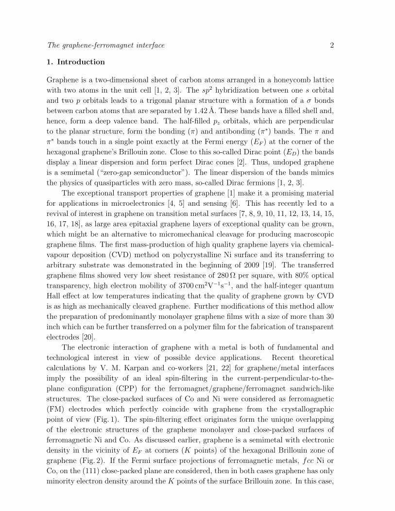
plane for (a,b) fcc Co (majority and minority spins), (c,d) fcc Ni (majority and
minority spins), and (e) fcc Cu. For graphene (f), the constant-energy surface is
centered in the K point of the two-dimensional interface Brillouin zone. Right-hand
panel: the results of band structure calculations (majority and minority spins) for (g)
fcc − hcp (BC) and (h,i) top − fcc (AC) configurations of carbon atoms on Ni(111).
The weight of the carbon πz character is shown by black lines where its thickness
reflects corresponding orbital weight. Reprinted figures with permission from V. M.
Karpan et al., Phys. Rev. B 78, 195419 (2008). Copyright (2008) by the American
Physical Society.
unoccupied states. This leads to the appearance of the induced magnetic moment of
µ = 0.05− 0.1µB on the carbon atoms in the graphene layer that is confirmed by both
x-ray magnetic circular dichroism (XMCD) and spin-resolved photoemission (PES).
Angle-resolved photoemission (ARPES) data confirm the strong interaction between
graphene and Ni(111) showing considerable modification of the valence-band states of
Ni and graphene due to hybridization. The three-dimensional (3D) mapping of electronic
states gives full information about the band structure of the graphene/Ni(111) system.
Detailed analysis of the Fermi surface of the graphene/Ni(111) system indicates very
good agreement between experimental and calculated 2D pictures of electronic states in
the valence band.
2. Experimental details
The present studies of the graphene/Ni(111) interface were performed in different
experimental stations in identical experimental conditions allowing for the reproducible
sample quality in different experiments. In all experiments the W(110) single crystal
was used as a substrate. Prior to preparation of the graphene/Ni(111) system the well-
established cleaning procedure of the tungsten substrate was applied: several cycles of
oxygen treatment with subsequent flashes to 2300 C. A well-ordered Ni(111) surface
was prepared by thermal deposition of Ni films with a thickness of more than 200 A on
to a clean W(110) substrate and subsequent annealing at 300 C. An ordered graphene
overlayer was prepared via thermal decomposition of propene (C3H6) according to the
recipe described elsewhere [8, 9, 25, 26, 27]. The quality, homogeneity, and cleanliness
of the prepared graphene/Ni(111) system was verified by means of LEED, STM, and
core-level as well as valence-band photoemission.
STM experiments were carried out in an ultra-high vacuum (UHV) system (base
pressure 8 × 10⁻¹¹ mbar) equipped with an Omicron variable temperature scanning
The graphene-ferromagnet interface 5
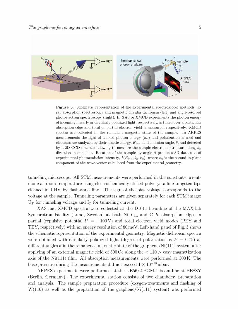
Figure 3. Schematic representation of the experimental spectroscopic methods: x-
ray absorption spectroscopy and magnetic circular dichroism (left) and angle-resolved
photoelectron spectroscopy (right). In XAS or XMCD experiments the photon energy
of incoming linearly or circularly polarized light, respectively, is tuned over a particular
absorption edge and total or partial electron yield is measured, respectively. XMCD
spectra are collected in the remanent magnetic state of the sample. In ARPES
measurements the light of a fixed photon energy (hν) and polarization is used and
electrons are analyzed by their kinetic energy, Ekin, and emission angle, θ, and detected
by a 2D CCD detector allowing to measure the sample electronic structure along kxdirection in one shot. Rotation of the sample by angle β produces 3D data sets of
experimental photoemission intensity, I(Ekin, kx, ky), where ky is the second in-plane
component of the wave-vector calculated from the experimental geometry.
tunneling microscope. All STM measurements were performed in the constant-current-
mode at room temperature using electrochemically etched polycrystalline tungsten tips
cleaned in UHV by flash-annealing. The sign of the bias voltage corresponds to the
voltage at the sample. Tunneling parameters are given separately for each STM image:
UT for tunneling voltage and IT for tunneling current.
XAS and XMCD spectra were collected at the D1011 beamline of the MAX-lab
Synchrotron Facility (Lund, Sweden) at both Ni L2,3 and C K absorption edges in
partial (repulsive potential U = −100 V) and total electron yield modes (PEY and
TEY, respectively) with an energy resolution of 80 meV. Left-hand panel of Fig. 3 shows
the schematic representation of the experimental geometry. Magnetic dichroism spectra
were obtained with circularly polarized light (degree of polarization is P = 0.75) at
different angles θ in the remanence magnetic state of the graphene/Ni(111) system after
applying of an external magnetic field of 500 Oe along the < 110 > easy magnetization
axis of the Ni(111) film. All absorption measurements were performed at 300 K. The
base pressure during the measurements did not exceed 1× 10⁻¹⁰ mbar.
ARPES experiments were performed at the UE56/2-PGM-1 beam-line at BESSY
(Berlin, Germany). The experimental station consists of two chambers: preparation
and analysis. The sample preparation procedure (oxygen-treatments and flashing of
W(110) as well as the preparation of the graphene/Ni(111) system) was performed
The graphene-ferromagnet interface 6
in the preparation chamber after which sample was transferred into the analysis
chamber for further photoemission measurements. The photoemission intensity data
sets I(E, kx, ky) were collected with a PHOIBOS 100 energy analyzer (SPECS) while
the graphene/Ni(111)/W(110) sample was placed on a 6-axes manipulator (3 translation
and 3 rotation axes) (Fig. 3, right-handel panel). The temperature of the sample during
the measurements was kept at 80 K or 300 K. The energy/angular resolution was set to
80 meV/0.2. In case of the spin-resolved PES experiments the mini-Mott-spin-detector
(SPECS) was used instead of the 2D CCD detector. The spin-resolved spectra were
collected in the remanent magnetic state of the graphene/Ni(111) system (see above)
in normal emission geometry. The effective Sherman function was estimated to be
Seff = 0.1 and instrumental asymmetry was accounted via measuring of spin-resolved
spectra for two opposite directions of the sample magnetization. The base pressure
during all photoemission measurements was below 7× 10⁻¹¹ mbar.
3. Results and discussion
3.1. Growth and surface structure of graphene on Ni(111)
In order to check the quality of the samples directly after each preparation step as well as
to provide structural details of the graphene sheets at the atomic level, we performed in
situ STM measurements at room temperature. Figure 4(a) shows an STM image of the
clean atomically flat W(110) surface. The (1× 1) LEED pattern of two-fold symmetry
[inset in Fig. 4(a)], typical for the bcc W(110) surface, confirms its high quality. The
surface morphology of a 200 A-thick Ni(111) film deposited on W(110) is shown in
Fig. 4(b). Atomically flat terraces separated by steps are visible in the STM image give
clear evidence of the epitaxial growth of Ni(111). After the Ni deposition a well-ordered
hexagonal (1 × 1) LEED pattern was observed [inset of Fig. 4(b)]. Since Ni(111) and
graphene have the nearly similar lattice parameters (the lattice mismatch is of only
1.3 %), graphene forms the hexagonal (1× 1) structure. Fig. 4(c) shows an overview of
a graphene domain on Ni(111) after thermal decomposition of propene. The graphene
layer is continuous and exhibits a highly ordered crystallographic structure without any
visible defects even over large areas. Fig. 4(d) represents a magnified topographic image
of the graphene lattice together with a typical LEED pattern of monolayer graphene on
Ni(111) [inset of Fig. 4(d)]. A higher magnification STM image of the graphene surface
is shown in Fig. 4(e) with the graphene hexagonal unit cell marked in the image.
So far several possible atomic configurations were considered for the
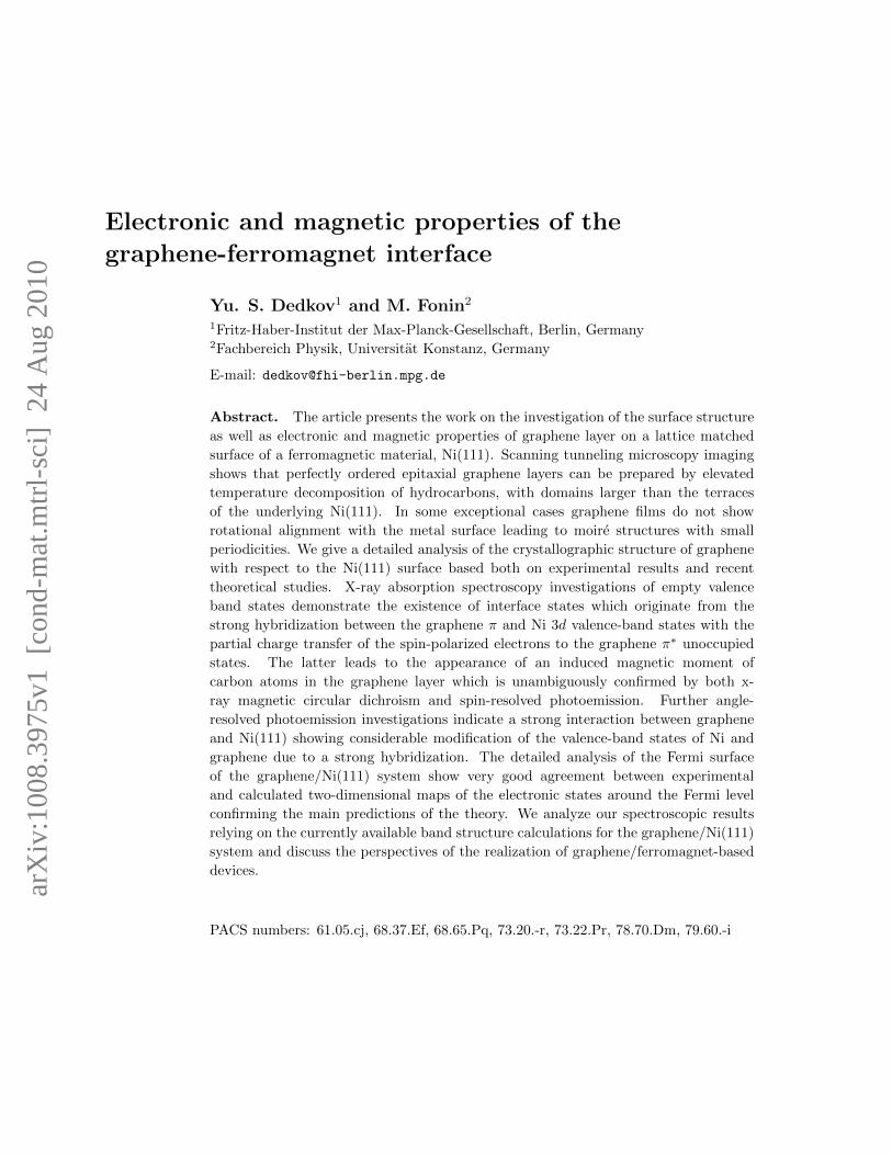
graphene/Ni(111) intrface. Three “high-symmetry” structures are known as hcp− fcc,top−hcp, and top−fcc and they are shown in Figs. 1(a-c), respectively. In the top−hcpconfiguration, the C atoms are placed directly above the Ni atoms of the first layer (top
site) and the second layer (hcp site). In top − fcc, the C atoms are arranged above
the Ni atoms of the first and third (fcc) layers. In the hcp − fcc configuration, the C
atoms are placed above hcp and fcc sites. Three additional configurations were consid-
The graphene-ferromagnet interface 7
Figure 4. (a) Large scale STM image of the W(110) surface showing atomically
flat terraces. Tunneling parameters: UT = 0.8 V; IT = 11 nA. Inset: a LEED image
of the W(110) surface taken at a primary electron energy of 69 eV. (b) Large scale
STM image of the epitaxial Ni(111) layer grown on the W(110) substrate. Tunneling
parameters: UT = 0.5 V; IT = 0.7 nA. Inset: a LEED image of the Ni(111) surface taken
at a primary electron energy of 67 eV. (c-e) High-quality graphene/Ni(111) system. (c)
Large scale constant current STM image of the graphene/Ni(111) surface. Tunneling
parameters: U = 0.002 V; I = 48 nA. (d) Magnified STM image of the perfect graphene
lattice. The inset shows a LEED image obtained at 63 eV. (e) High magnification STM
image showing atomic structure of the graphene monolayer. Tunneling parameters:
UT = 0.002 V; I = 48 nA). Graphene hexagonal unit cell is marked in (e).
The graphene-ferromagnet interface 8
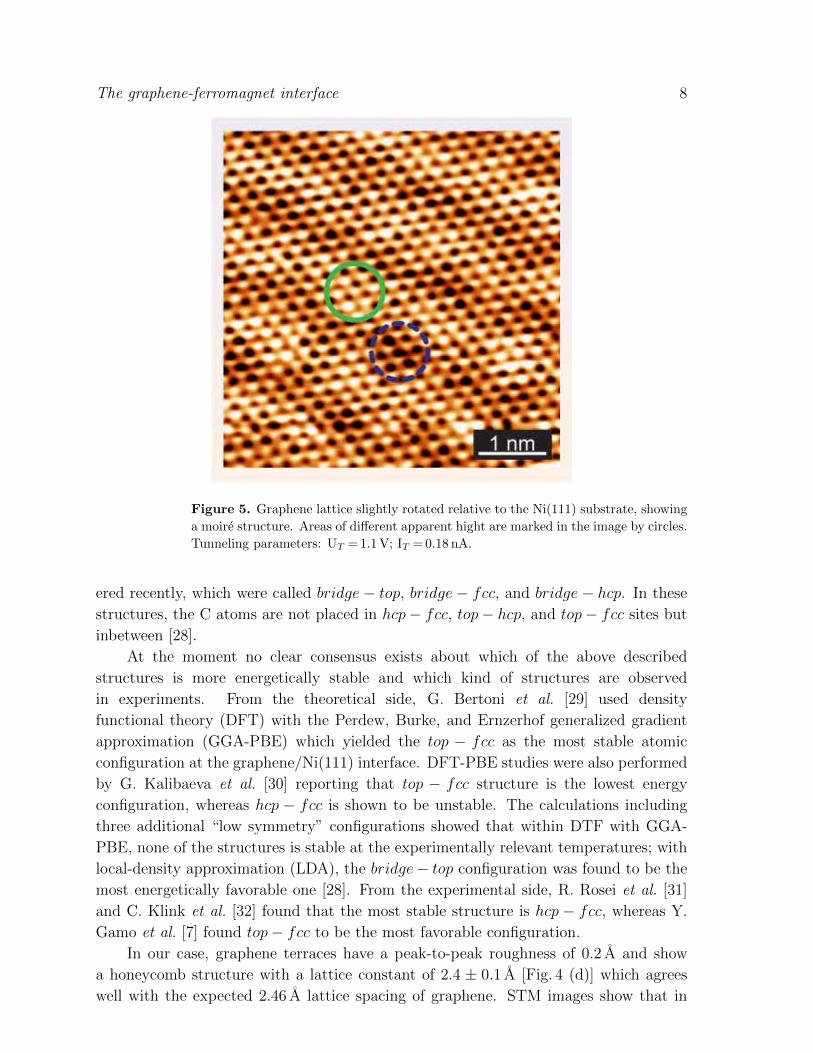
Figure 5. Graphene lattice slightly rotated relative to the Ni(111) substrate, showing
a moire structure. Areas of different apparent hight are marked in the image by circles.
Tunneling parameters: UT = 1.1 V; IT = 0.18 nA.
ered recently, which were called bridge− top, bridge− fcc, and bridge− hcp. In these
structures, the C atoms are not placed in hcp− fcc, top− hcp, and top− fcc sites but
inbetween [28].
At the moment no clear consensus exists about which of the above described
structures is more energetically stable and which kind of structures are observed
in experiments. From the theoretical side, G. Bertoni et al. [29] used density
functional theory (DFT) with the Perdew, Burke, and Ernzerhof generalized gradient
approximation (GGA-PBE) which yielded the top − fcc as the most stable atomic
configuration at the graphene/Ni(111) interface. DFT-PBE studies were also performed
by G. Kalibaeva et al. [30] reporting that top − fcc structure is the lowest energy
configuration, whereas hcp − fcc is shown to be unstable. The calculations including
three additional “low symmetry” configurations showed that within DTF with GGA-
PBE, none of the structures is stable at the experimentally relevant temperatures; with
local-density approximation (LDA), the bridge− top configuration was found to be the
most energetically favorable one [28]. From the experimental side, R. Rosei et al. [31]
and C. Klink et al. [32] found that the most stable structure is hcp − fcc, whereas Y.
Gamo et al. [7] found top− fcc to be the most favorable configuration.
In our case, graphene terraces have a peak-to-peak roughness of 0.2 A and show
a honeycomb structure with a lattice constant of 2.4 ± 0.1 A [Fig. 4 (d)] which agrees
well with the expected 2.46 A lattice spacing of graphene. STM images show that in
The graphene-ferromagnet interface 9
the honeycomb unit cell carbon atoms corresponding to different sites appear with a
different contrast, which can be attributed to the differences in the local stacking of
the graphene sheet and the Ni(111) substrate. Therefore we interpret our STM images
in the following way: Fig. 4 shows a single layer graphene, where carbon atoms most
possibly occupy positions corresponding to one of the two non-equivalent configurations
– top − fcc or top − hcp. However, it turns to be impossible to directly identify which
of the sites are occupied.
Additionally, some different orientations of the graphene relative to the Ni(111)
substrate could be observed. Fig. 5 shows a moire structure, indicating a slight rotation
of the graphene layer relative to the Ni(111) substrate demonstrating the simultaneous
existence of different stackings in the graphene/Ni(111) system. Two regions showing
different apparent heights can be distinguished on the surface (see Fig. 5). This
observation shows that although the interaction between nickel and graphene is relatively
strong, different adsorption geometries are locally possible. We would like to note, that
such areas represent an very rare case compared with the normal graphene structure as
supported by STM, LEED and photoemission measurements.
3.2. Bonding and magnetism at the graphene/Ni(111) interface
In order to address the average spatial orientation of selected molecular orbitals (for
example π or σ) at the graphene/Ni interface, we vary the sample orientation with
respect to the wave vector of the linearly polarized x-ray light and monitor the absorption
intensity. The observed changes of the XAS lineshape at the C K edge in the
graphene/Ni(111) system represent a nice example demonstrating the so-called search-
light-like effect [33], which in general can be used for probing of the quadrupole moment
of the local charge around the absorbing atom. In such an experiment, the absorption
intensity associated with a specific molecular orbital final state has a maximum if the
electric field vector is aligned parallel to the direction of maximum charge or hole density,
i. e. along a molecular orbital, and the intensity vanishes if the electric field vector is
perpendicular to the orbital axis. The detailed description of the angular dependence
of XAS intensities can be found elsewhere [33, 34].
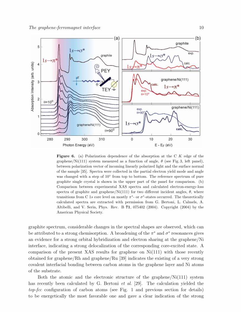
Figure 6 (a) shows XAS spectra of the graphene/Ni(111) system recorded at the C
K absorption edge as a function of the angle, θ, between the direction of the incident
linearly polarized x-ray light and the sample surface, e. g. between the electrical field
vector of light and the sample surface normal (see the inset of Fig. 6 for the exact
geometry of the experiment). The reference XAS spectrum of the graphite single
crystal measured at θ = 30 is shown in the upper part of the figure. The spectral
features in the two broad regions 283 − 289 eV and 289 − 295 eV can be ascribed to C
1s → π∗ and C 1s → σ∗ transitions of core electrons into unoccupied states (π∗, σ∗1,
and σ∗2), respectively. The XAS line shape in both regions is influenced by considerable
excitonic effects – poor core-hole screening [36, 37, 38]. Upon the comparison of the
XAS C 1s → π∗, σ∗ spectrum of the graphene/Ni(111) system with the reference
The graphene-ferromagnet interface 10
Figure 6. (a) Polarization dependence of the absorption at the C K edge of the
graphene/Ni(111) system measured as a function of angle, θ (see Fig. 3, left panel),
between polarization vector of incoming linearly polarized light and the surface normal
of the sample [35]. Spectra were collected in the partial electron yield mode and angle
was changed with a step of 10 from top to bottom. The reference spectrum of pure
graphite single crystal is shown in the upper part of the panel for comparison. (b)
Comparison between experimental XAS spectra and calculated electron-energy-loss
spectra of graphite and graphene/Ni(111) for two different incident angles, θ, where
transitions from C 1s core level on mostly π∗- or σ∗-states occurred. The theoretically
calculated spectra are extracted with permission from G. Bertoni, L. Calmels, A.
Altibelli, and V. Serin, Phys. Rev. B 71, 075402 (2004). Copyright (2004) by the
American Physical Society.
graphite spectrum, considerable changes in the spectral shapes are observed, which can
be attributed to a strong chemisorption. A broadening of the π∗ and σ∗ resonances gives
an evidence for a strong orbital hybridization and electron sharing at the graphene/Ni
interface, indicating a strong delocalization of the corresponding core-excited state. A
comparison of the present XAS results for graphene on Ni(111) with those recently
obtained for graphene/Rh and graphene/Ru [39] indicates the existing of a very strong
covalent interfacial bonding between carbon atoms in the graphene layer and Ni atoms
of the substrate.
Both the atomic and the electronic structure of the graphene/Ni(111) system
has recently been calculated by G. Bertoni et al. [29]. The calculation yielded the
top-fcc configuration of carbon atoms (see Fig. 1 and previous section for details)
to be energetically the most favorable one and gave a clear indication of the strong
The graphene-ferromagnet interface 11
interaction between graphene layer and substrate. Similar results were obtained for
graphene/Co(0001) [40]. This interaction manifests itself by a considerable modification
of the graphene- and Ni-related valence band states as a result of the hybridization of
the graphene π and the Ni 3d states accompanied by a partial charge transfer of spin-
polarized electrons from ferromagnetic substrate to graphene. These calculations also
predict that several occupied and unoccupied interface states (I1 − I5) are formed in
this system which lead to noticeable modifications of the carbon K-edge electron energy
loss spectroscopy (EELS) spectrum. The detailed description of the electronic structure
of the graphene/Ni(111) system including the interface states will be given in the next
section in conjunction with the discussion of the angle-resolved photoemission results.
In the following we would like to compare our XAS results with the recently
calculated C K-edge EELS spectra for the graphene/Ni(111) interface [29]. In this
case, experimental XAS spectra taken at θ = 10 and θ = 90 correspond to the
calculated EELS spectra for the scattering vector q perpendicular and parallel to the
graphene layer, respectively. The calculated EELS spectra are found to agree well
with the experimental XAS data [see Fig. 6 (b)]: (i) the spectra show the same angle
(scattering vector) dependence and (ii) the experimentally observed XAS features are
well reproduced in the calculated EELS spectra. For example, two peaks in the XAS
spectra in the 1s → π∗ spectral region at 285.5 eV and 287.1 eV of photon energy can
be assigned to the double-peak structure in the calculated EELS spectrum at 0.8 eV
and 3.0 eV above the Fermi level [29]. According to the theoretical calculations [29], the
first sharp feature in the XAS spectrum is due to the transition of the electron from the
1s core level into the interface state I4 above the Fermi level (around the K point in
the hexagonal Brillouin zone) which originates from the C pz–Ni 3d hybridization and
corresponds to the antibonding orbital between a carbon atom C-top and an interface
Ni atom. The second peak in the XAS spectrum is due to the dipole transition of an
electron from the 1s core level into the interface state I5 above the Fermi level (around
the M -point in the hexagonal Brillouin zone) which originates from C pz–Ni px, py, 3d
hybridization and corresponds to a bonding orbital between C-top and C-fcc atoms,
involving a Ni interface atom. The small feature at 283.7 eV and the low-energy shoulder
in the 1s→ π∗ absorption spectra probably partly originate from the interface state I4which is located very close to the Fermi level. In case of the XAS C 1s→ σ∗, the theory
also correctly describes the shape of the absorption spectra [29].
The strong hybridization between graphene π and Ni 3d valence band states at
the graphene/Ni(111) interface leads to the partial charge transfer of the spin-polarized
electrons from Ni onto C with the appearance of an induced effective magnetic moment
of carbon atoms [29] which can be detected in an experiment which is sensitive to
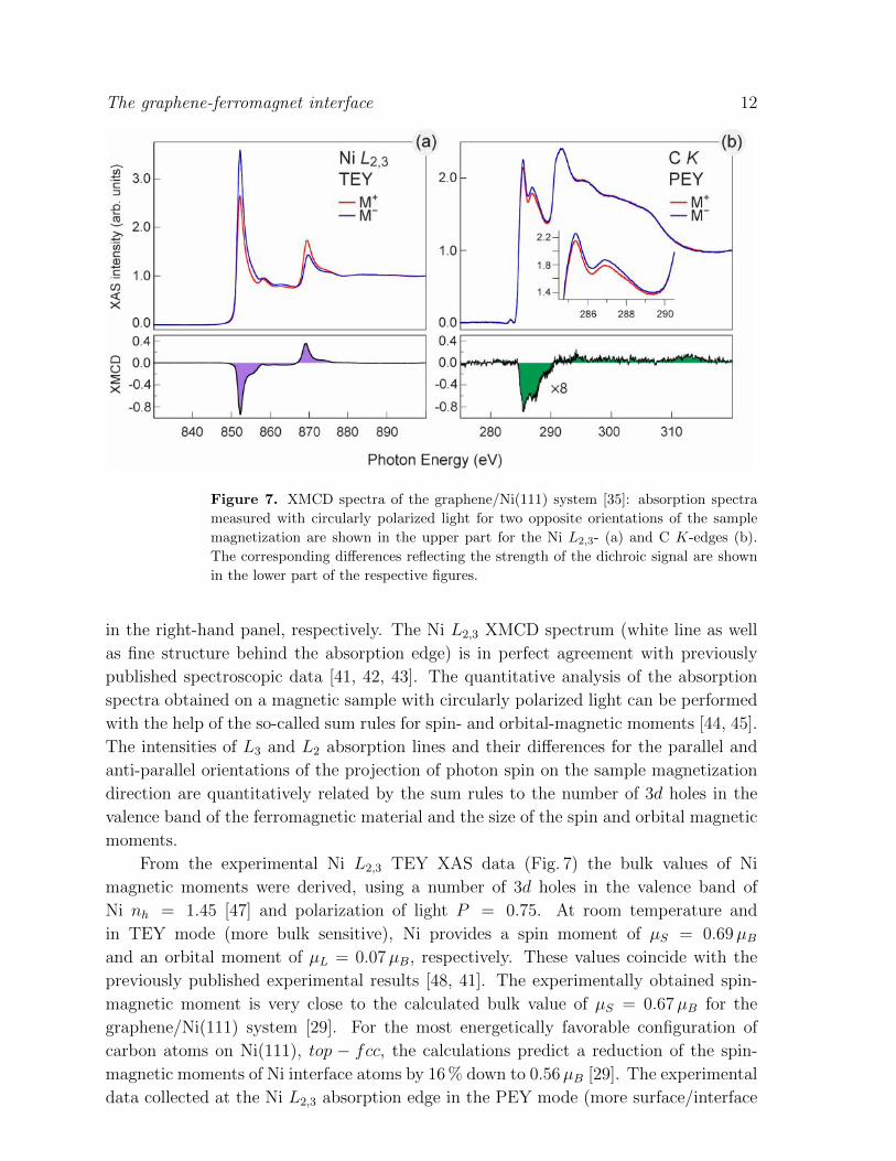
the magnetic state of particular element, like XMCD. Figure 7 shows XAS spectra of
the graphene/Ni(111) system obtained for two opposite magnetization directions with
respect to the polarization of the incident X-ray beam (upper panels) together with
the resulting XMCD signal (lower panels). The spectra collected at the Ni L2,3 edge in
TEY mode and at the C K edge in PEY mode are presented in the left-hand panel and
The graphene-ferromagnet interface 12
Figure 7. XMCD spectra of the graphene/Ni(111) system [35]: absorption spectra
measured with circularly polarized light for two opposite orientations of the sample
magnetization are shown in the upper part for the Ni L2,3- (a) and C K-edges (b).
The corresponding differences reflecting the strength of the dichroic signal are shown
in the lower part of the respective figures.
in the right-hand panel, respectively. The Ni L2,3 XMCD spectrum (white line as well
as fine structure behind the absorption edge) is in perfect agreement with previously
published spectroscopic data [41, 42, 43]. The quantitative analysis of the absorption
spectra obtained on a magnetic sample with circularly polarized light can be performed
with the help of the so-called sum rules for spin- and orbital-magnetic moments [44, 45].
The intensities of L3 and L2 absorption lines and their differences for the parallel and
anti-parallel orientations of the projection of photon spin on the sample magnetization
direction are quantitatively related by the sum rules to the number of 3d holes in the
valence band of the ferromagnetic material and the size of the spin and orbital magnetic
moments.
From the experimental Ni L2,3 TEY XAS data (Fig. 7) the bulk values of Ni
magnetic moments were derived, using a number of 3d holes in the valence band of
Ni nh = 1.45 [47] and polarization of light P = 0.75. At room temperature and
in TEY mode (more bulk sensitive), Ni provides a spin moment of µS = 0.69µB
and an orbital moment of µL = 0.07µB, respectively. These values coincide with the
previously published experimental results [48, 41]. The experimentally obtained spin-
magnetic moment is very close to the calculated bulk value of µS = 0.67µB for the
graphene/Ni(111) system [29]. For the most energetically favorable configuration of
carbon atoms on Ni(111), top − fcc, the calculations predict a reduction of the spin-
magnetic moments of Ni interface atoms by 16 % down to 0.56µB [29]. The experimental
data collected at the Ni L2,3 absorption edge in the PEY mode (more surface/interface
The graphene-ferromagnet interface 13
sensitive) also shows a slight reduction of the spin moment to µS = 0.63µB. However,
the observed decreasing is not so pronounced as yielded by the theoretical calculation,
which can be explained by the large contribution of the bulk-derived signal to the XMCD
spectra.
The most important and interesting results of these XMCD experiments on the
graphene/Ni(111) system is the observation of the relatively large dichroic contrast
at the C K absorption edge [Fig. 7(b)]. In order to magnify the measured magnetic
contrast at the 1s → π∗ absorption edge, these XMCD spectra were collected in the
PEY mode with the circularly polarized light at an angle of θ = 20. We note that the
observed differences in the XAS spectra collected at this angle visible in Figs. 6 and 7
are due to the different polarization of light: in Fig. 6(a) the data are obtained with the
linearly polarized x-rays, i. e. the strong angular dependence of the absorption signal
is due to the different graphene’s orbital orientation; whereas the data in Fig. 7 are
taken with the circularly polarized light, i. e. both 1s → π∗ and 1s → σ∗ transitions
are nearly equivalently possible. The C K XMCD spectrum reveals that the major
magnetic response stems from transitions of the 1s electron onto the π∗-states, while
transitions onto the σ∗-states yield very weak (if any) magnetic signal. These results
indicate that only the C 2pz orbitals of the graphene layer are magnetically polarized
due to the hybridization with the Ni 3d band. The sharp structure at the 1s → π∗
absorption edge originates from hybridized C pz–Ni 3d and C pz–Ni px, py 3d states (see
earlier discussion and Ref. [29]).
The appearance of XMCD signal at the C K-edge shows that indeed the Ni film
induces a magnetic moment in the graphene overlayer. However, at the C K absorption
edge, the electron transitions occur from the non-spin-orbit split 1s initial states to
the 2p final states and thus, in the analysis of the dichroism effect at the K edge one
equation in the selection rules is missed. This means that the XMCD signal at K
edges provides the information only on the orbital magnetic moment µorb [44, 45, 46].
The partial charge transfer from Ni to C atoms in the graphene/Ni(111) system was
calculated for the 22-atom (graphene)/Ni cluster [49] yielding 0.205e− per C atom in
graphene which leads to the 2p-orbital occupation number of np = 2.205e−. Using
the the C K XAS spectra the procedure described in work [46], the orbital magnetic
moment of µorb = 1.8 ± 0.6 × 10⁻³ µB per C atom was extracted. The relatively
large uncertainty arises mainly from the estimation of the number of C 2p holes, the
background subtraction of XAS spectra, and from the error for the degree of circular
polarization of light.
The theoretical work [29] also gives the values for the spin magnetic moment of
−0.01µB and 0.02µB for C-top and C-fcc atoms, respectively. However, the magnetic
splitting of the majority and minority parts of the interface states I3 and I4 was found
between 0.13 and 0.55 eV, respectively, which may yield higher values for the magnetic
moment. Due to the impossibility to directly extract the value of the spin magnetic
moment form the K edge XMCD spectra, we apply a simple comparison with the
magnetic measurements on similar systems in oder to estimate the average µS value
The graphene-ferromagnet interface 14
for the carbon atoms at the graphene/Ni(111) interface. For the Fe/C multilayers clear
magnetic signals of carbon were obtained by using the resonant magnetic reflectivity
technique [50]. Hysteresis loop recorded at C K absorption edge gave a clear proof of
ferromagnetism of carbon atoms at room temperature with a measured spin magnetic
moment of µS = 0.05µB induced by adjacent Fe atoms. The observed ferromagnetism
of carbon in the Fe/C multilayered system was related to the hybridization between
the Fe 3d orbitals and the C pz orbitals which are normal to the graphene-type layered
sp2-coordination. The second comparison can be performed with carbon nanotubes on
ferromagnetic Co substrate [51]. Carbon nanotubes were shown to become magnetized
when they are in contact with magnetic material. Spin-polarized charge transfer at
the interface between a flat ferromagnetic metal substrate and a multiwalled carbon
nanotube leads to a spin transfer of about 0.1µB per contact carbon atom. Additionally,
a comparison of the XMCD spectra obtained at the C K edge in graphene/Ni(111)
(present work) and at the O K edge in O/Ni(100) [52], reveals the approximately
same magnitude of the XMCD signal. For the O/Ni(100) system, where the induced
spin-magnetic moment of 0.053µB on oxygen atom was calculated, the theoretically
simulated XAS and XMCD spectra agree well with the experimental data. Considering
these analogous systems, we estimate the induced magnetic moment for graphene on
Ni(111) to be in the range of 0.05-0.1 µB per carbon atom.
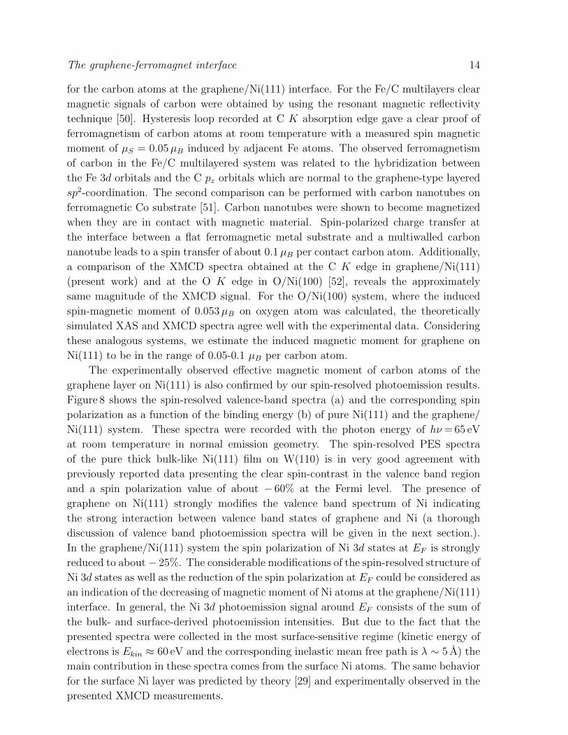
The experimentally observed effective magnetic moment of carbon atoms of the
graphene layer on Ni(111) is also confirmed by our spin-resolved photoemission results.
Figure 8 shows the spin-resolved valence-band spectra (a) and the corresponding spin
polarization as a function of the binding energy (b) of pure Ni(111) and the graphene/
Ni(111) system. These spectra were recorded with the photon energy of hν= 65 eV
at room temperature in normal emission geometry. The spin-resolved PES spectra
of the pure thick bulk-like Ni(111) film on W(110) is in very good agreement with
previously reported data presenting the clear spin-contrast in the valence band region
and a spin polarization value of about − 60% at the Fermi level. The presence of
graphene on Ni(111) strongly modifies the valence band spectrum of Ni indicating
the strong interaction between valence band states of graphene and Ni (a thorough
discussion of valence band photoemission spectra will be given in the next section.).
In the graphene/Ni(111) system the spin polarization of Ni 3d states at EF is strongly
reduced to about− 25%. The considerable modifications of the spin-resolved structure of
Ni 3d states as well as the reduction of the spin polarization at EF could be considered as
an indication of the decreasing of magnetic moment of Ni atoms at the graphene/Ni(111)
interface. In general, the Ni 3d photoemission signal around EF consists of the sum of
the bulk- and surface-derived photoemission intensities. But due to the fact that the
presented spectra were collected in the most surface-sensitive regime (kinetic energy of
electrons is Ekin ≈ 60 eV and the corresponding inelastic mean free path is λ ∼ 5 A) the
main contribution in these spectra comes from the surface Ni atoms. The same behavior
for the surface Ni layer was predicted by theory [29] and experimentally observed in the
presented XMCD measurements.
The graphene-ferromagnet interface 15
Figure 8. (a) Spin-resolved PES spectra and (b) corresponding spin polarization of
Ni 3d valence band states as a function of the binding energy for Ni(111) and the
graphene/ Ni(111) system. (c) Spin-resolved photoemission spectra of the π-states of
graphene on Ni(111). A spin polarization value of about (−12 ± 2%) together with
a considerable π-band exchange splitting of about 34 meV are observed. All spectra
were collected in the normal emission geometry with the photon energy of 65 eV.
Fig. 8(c) shows the spin-resolved spectra of the π states of graphene on Ni(111)
measured in normal emission geometry with the photon energy of 65 eV. These states
are located at 10.1 eV of binding energy (see next section for details). After the careful
subtraction of the background spin-polarization which originates from the spin-resolved
Ni 3d valence band states the clear spin contrast could be detected for the graphene
π states with the maximum spin-polarization of P = −12 ± 2 % at room temperature.
The two spin-resolved components are fitted with Lorenzian-shape profiles giving the
exchange splitting of about 34 ± 9 meV for these state which agrees well with the
value extracted from theoretical work [29]. A comparison of the spin-resolved spectra
with the background spin polarization originating from Ni 3d states shows that the
spin moment of graphene is aligned antiparallel to the magnetization of Ni meaning
antiparallel magnetic coupling of graphene to Ni. However, this conclusion is based
only upon the normal emission spin-resolved measurements and has to be clarified by
more detailed spin-resolved PES experiments. Here we would like to note, that the
experimental evidence of a pronounced spin polarization at room temperature together
with the splitting of the π states in the graphene/Ni(111) system are in contradiction to
the results previously reported by O. Rader et al. [53], where the absence or very small
spin-polarization of the graphene π states was observed. The origin of this discrepancy
is however not clear at the moment and further spin-polarized PES investigations of the
graphene/Ni(111) system should be undertaken in order to resolve this issue.
The graphene-ferromagnet interface 16
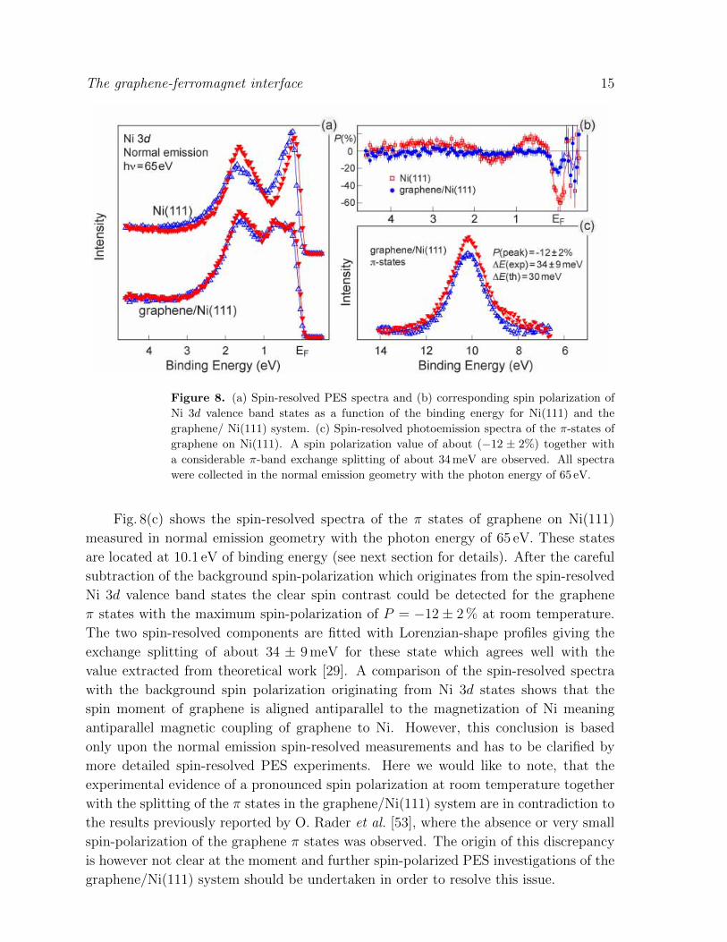
Figure 9. Angle-resolved photoemission spectra of the graphene/Ni(111) system
recorded along the Γ −K direction of the hexagonal Brillouin zone at (a) 70 eV and
(b) 100 eV of photon energy. Spectra corresponding to Γ and K points are marked by
thick black lines.
3.3. Electronic properties of graphene on Ni(111)
Fig. 9 shows two series of angle-resolved photoemission spectra measured along the Γ−Kdirection of the hexagonal Brillouin zone of the graphene/Ni(111) system. Each series
is extracted from the 3D sets of data of photoemission intensity I(EB, kx, ky), where EB
is the binding energy and kx, ky are the orthogonal components of the in-plane wave
vector. For the graphene/Ni(111) system the K and M points of the Brillouin zone
are reached at 1.7 A−1 and at 1.4 A−1, respectively. Photoemission data presented in
Fig. 9 were collected at two different photon energies: 70 eV (a) and 100 eV (b). The
variation of the photon energy, i. e. photoemission cross-section, gives a possibility to
clearly separate the partial contributions of emissions from graphene-derived and Ni-
derived valence band states in the spectra. The presented photoemission data are in very
good agreement with previously published results [25, 54, 26, 8, 55], but acquired with
a much better energy/wave-vector resolution allowing for a more accurate analysis of
The graphene-ferromagnet interface 17
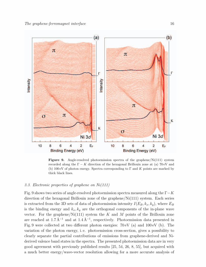
Figure 10. Regions around the K point of photoemission intensity of the
graphene/Ni(111) system measured at (a) 70 eV and (b) 100 eV of photon energy.
The corresponding intensity profiles at the K point are shown in the lower panels with
arrows indicating the main photoemission features discussed in the text.
photoemission dispersions. In Fig. 9 one can clearly discriminate dispersions of graphene
π- and σ-derived states in the region below 2 eV of the binding energy (BE) as well as
Ni 3d-derived states near EF . The binding energy of the graphene π states in the
center of the Brillouin zone (in the Γ point) equals to 10.1 eV which is approximately
by 2.4 eV larger than the binding energy of these states in pure graphite. The shift
to larger binding energy is different for σ and π valence band graphene-derived states.
This behavior can be explained by the different hybridization strength between these
states and Ni 3d valence band states which is larger for the out-of-plane oriented π
states compared with the one for the in-plane oriented σ states of the graphene layer.
The binding energy difference of ≈ 2.4 eV for the π states and ≈ 1 eV for the σ states
between graphite and graphene on Ni(111) is in good agreement with previously reported
experimental and theoretical values [8, 29]. The effect of hybridization between Ni 3d
and graphene π states can be clearly demonstarted in the region around the K point of
the Brillouin zone: (i) one of the Ni 3d bands at 1.50 eV changes its binding energy by
≈ 150 meV to larger BE when approaching the K-point; (ii) a hybridization shoulder
is visible in photoemission spectra which disperses from approximately 1.6 eV to the
binding energy of the graphene π states at the K point (see also Fig. 10 for a detailed
view). The strong hybridization observed in PES spectra underlines the fact that the
π states might become spin-polarized and might gain a non zero-magnetic moment due
to charge transfer from the Ni atoms to the carbon atoms.
Considering the electronic band structure of the graphene/Ni(111), the region
around the K point delivers the most interesting and important information
with respect to the possible spin-filtering effects in the graphene/ferromagnet or
ferromagnet/graphene/ferromagnet sandwich-like structures. This part of the electronic
structure measured with two different photon energies (hν = 70 eV and 100 eV) is shown
in Fig. 10 as color maps (upper panels) together the corresponding intensity profiles
The graphene-ferromagnet interface 18
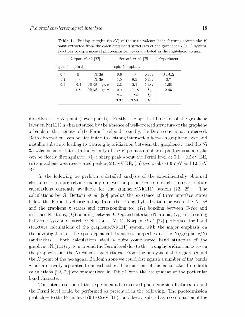
Table 1. Binding energies (in eV) of the main valence band features around the K
point extracted from the calculated band structures of the graphene/Ni(111) system.
Positions of experimental photoemission peaks are listed in the right-hand column.
Karpan et al. [22] Bertoni et al. [29] Experiment
spin ↑ spin ↓ spin ↑ spin ↓
0.7 0 Ni 3d 0.8 0 Ni 3d 0.1-0.2
1.2 0.9 Ni 3d 1.5 0.9 Ni 3d 0.7
0.1 -0.2 Ni 3d – gr.π 2.8 2.1 Ni 3d 1.65
1.8 Ni 3d – gr.π 0.2 -0.18 I3 2.65
2.4 1.96 I23.37 3.24 I1
directly at the K point (lower panels). Firstly, the spectral function of the graphene
layer on Ni(111) is characterized by the absence of well-ordered structure of the graphene
π-bands in the vicinity of the Fermi level and secondly, the Dirac-cone is not preserved.
Both observations can be attributed to a strong interaction between graphene layer and
metallic substrate leading to a strong hybridization between the graphene π and the Ni
3d valence band states. In the vicinity of the K point a number of photoemission peaks
can be clearly distinguished: (i) a sharp peak about the Fermi level at 0.1− 0.2 eV BE,
(ii) a graphene π-states-related peak at 2.65 eV BE, (iii) two peaks at 0.7 eV and 1.65 eV
BE.
In the following we perform a detailed analysis of the experimentally obtained
electronic structure relying mainly on two comprehensive sets of electronic structure
calculations currently available for the graphene/Ni(111) system [22, 29]. The
calculations by G. Bertoni et al. [29] predict the existence of three interface states
below the Fermi level originating from the strong hybridization between the Ni 3d
and the graphene π states and corresponding to: (I1) bonding between C-fcc and
interface Ni atoms; (I2) bonding between C-top and interface Ni atoms; (I3) antibonding
between C-fcc and interface Ni atoms. V. M. Karpan et al. [22] performed the band
structure calculations of the graphene/Ni(111) system with the major emphasis on
the investigation of the spin-dependent transport properties of the Ni/graphene/Ni
sandwiches. Both calculations yield a quite complicated band structure of the
graphene/Ni(111) system around the Fermi level due to the strong hybridization between
the graphene and the Ni valence band states. From the analysis of the region around
the K point of the hexagonal Brillouin zone we could distinguish a number of flat bands
which are clearly separated from each other. The positions of the bands taken from both
calculations [22, 29] are summarized in Table 1 with the assignment of the particular
band character.
The interpretation of the experimentally observed photoemission features around
the Fermi level could be performed as presented in the following. The photoemission
peak close to the Fermi level (0.1-0.2 eV BE) could be considered as a combination of the
The graphene-ferromagnet interface 19
interface state I3 (both spins) with a large contribution of the graphene π-character and
the Ni 3d(↓)-band. The second peak at 0.7 eV BE could be assigned to the combination
of the Ni 3d(↑)- and Ni 3d(↓)-bands present in both calculations (first and second rows
in Table 1, respectively). The feature at 1.65 eV could be considered as a combination of
Ni 3d(↑)-band and I2(↓)-state with a large graphene π-character. The last photoemission
peak (2.65 eV BE) could be assigned to the interface state I2(↑) with large contribution
of the graphene π-character.
In order to check the theoretical predictions concerning the CPP spin-dependent
electronic transport properties of the ideal graphene/Ni(111) interface, we perform a
careful analysis of the constant energy photoemission maps close to the Fermi level.
We would like to admit that such an analysis can be rather complicated due to the
fact that Ni 3d bands, which dominate the photoemission intensity around the Fermi
level, are very flat in the vicinity of EF . Figure 11 shows the constant energy cuts of
the 3D data set obtained at hν=100 eV for the graphene/Ni(111) system. These energy
cuts were taken at (a) 4 eV and (b) 2.7 eV of BE as well as at (c) the Fermi level.
The energy cut at EB = 4 eV shows characteristic photoemission intensity patterns of
the graphene layer which reflect the symmetry of the system. Below the Dirac point
(crossing of straight dispersion lines of π states in free-standing graphene) the graphene
π bands are visible in the first Brillouin zone whereas no bands can be seen in the
second one. Additionally several energy bands are present in the middle of the Brillouin
zone (outlined by dashed yellow lines) which also show hexagonal symmetry. These
bands originate from the hybridization of the Ni and graphene valence band states. The
constant energy cut taken in the region of the minimal binding energy of the graphene
π states (EB = 2.7 eV) is shown in Fig. 11(b). In the case of graphene/Ni(111) the
Dirac point is not preserved due to the strong hybridization of Ni 3d and graphene π
states around the K point. This can also be directly recognized at this energy cut where
graphene π states produce broad intensity spots instead of sharp points in the wave-
vector space. As in the previous case, we observe a number of valence band states in the
middle part of the Brillouin zone which again could be assigned to the hybridization-
derived states.
The most interesting and important information in view on the spin-dependent
transport properties of the graphene/Ni(111) system, can be extracted form the constant
energy cut obtained at the Fermi energy which is presented at Fig. 11(c). Already the
analysis of Figs. 9(a,b) and 10(a,b) shows that the photoemission intensity is increased
around the K point and along the K−M direction of the hexagonal Brillouin zone, that
correlates with the increased photoemission intensity observed in the energy cut shown
in Fig. 11(c) for the Fermi energy. Additionally, a number of arcs surrounding the
K points and weak (but distinguished) diamond-shape regions of increased intensity
is clearly visible in the middle part and around the M points of the Brillouin zone,
respectively. Upon the comparison of the obtained photoemission results for the
graphene/Ni(111) system (Figs. 9–11) with the band structure calculations for this
system (Fig. 2) [21, 22, 29], we find very good agreement between theory and experiment.
The graphene-ferromagnet interface 20
Figure 11. Constant energy cuts of the 3D data sets in the energy-wave vector space,
I(EB , kx, ky), obtained via a β-scan of the graphene/Ni(111) system obtained at 100 eV
of photon energy. The energy cuts are taken at (a) 4 eV and (b) 2.7 eV BE as well as at
(c) EF . As a supplementary we also present a movie which chows the binding energy
scan through the valence band of the graphene/Ni(111) system with corresponding
energy cuts in the wave-vector space. Dashed lines are guides to the eye.
Particularly, the region around the Fermi level for the ideal graphene/Ni(111) system
is well reproduced in the experiment, confirming the main predictions of the theory.
Unfortunately, at the present stage of the experiment, we can not specify the spin-
character of energy bands, which should be the subject of future spin- and angle-resolved
photoemission investigations.
4. Conclusions
In conclusion, structural, magnetic and electronic properites of the high-quality
graphene/ferromagnet interface [graphene on Ni(111)] were investigated by means of
scanning tunneling microscopy, x-ray absorption spectroscopy and magnetic circular
dichroism as well as via mapping of the band structure by means of angle-resolved
photoemission. STM investigation shows that perfectly ordered epitaxial graphene
layers can be prepared by elevated temperature decomposition of hydrocarbons, with
domains larger than the terraces of the underlying Ni(111). A strong modification
of the electronic structure of the graphene layer and Ni substrate upon graphene
adsorption on the ferromagnetic substrate was detected by all spectroscopic methods.
This modification is due to the considerable hybridization of the graphen π and Ni
3d valence band states accompanied by the partial charge transfer of spin-polarized
electrons from Ni onto C atoms leading to the appearance of the effective magnetic
moment in the graphene layer. The presence of an effective magnetic moment on carbon
atoms of the graphene layer was unambigously proven by XMCD and spin-resolved
The graphene-ferromagnet interface 21
photoemission measurements. The experimentally obtained electronic structure of
occupied and unoccupied states was compared with available band structure calculations
allowing the clear assignment of spectral features in the XAS and ARPES data. The
good agreement between theory and experiment was also found upon the analysis of the
Fermi energy cuts, that give us an opportunity to confirm the main statements of the
theoretical works predicting the spin-filtering effects of the graphene/Ni(111) interface.
However, the clear assignment of the spectroscopic valence band features have to be
performed in future spin-resolved photoemission experiments.
Acknowledgements
We would like to thank all co-workers and collaborators for their contributions
to this work, in particular, K. Horn, M. Weser, S. Bottcher, C. Enderlein, A.
Preobrajenski, E. Voloshina, M. Sicot, P. Leicht, A. Zusan. We are also grateful
to P. Kelly and L. Calmels for fruitful discussions. This work has been supported
by the European Science Foundation (ESF) under the EUROCORES Programme
EuroGRAPHENE (Project “SpinGraph”). M. F. gratefully acknowledges the financial
support by the Research Center “UltraQuantum” (Excellence Initiative), by the
Deutsche Forschungsgemeinschaft (DFG) via the Collaborative Research Center (SFB)
767, and the Baden-Wurttemberg Stiftung.
References
[1] A K Geim and K S Novoselov. The rise of graphene. Nature Mater., 6:183, 2007.
[2] A Castro Neto, F Guinea, N Peres, K Novoselov, and A Geim. The electronic properties of
graphene. Rev. Mod. Phys., 81:109, 2009.
[3] A K Geim. Graphene: Status and prospects. Science, 324:1530, 2009.
[4] K S Novoselov, A K Geim, S V Morozov, D Jiang, M I Katsnelson, I V Grigorieva, S V Dubonos,
and A A Firsov. Two-dimensional gas of massless dirac fermions in graphene. Nature, 438:197,
2005.
[5] S V Morozov, K S Novoselov, M I Katsnelson, F Schedin, D C Elias, J A Jaszczak, and A K Geim.
Giant intrinsic carrier mobilities in graphene and its bilayer. Phys. Rev. Lett., 100:016602, 2008.
[6] F Schedin, A. K Geim, S V Morozov, E W Hill, P Blake, M I Katsnelson, and K S Novoselov.
Detection of individual gas molecules adsorbed on graphene. Nature Mater., 6:652, 2007.
[7] Y Gamo, A Nagashima, M Wakabayashi, M Terai, and C Oshima. Atomic structure of monolayer
graphite formed on Ni(111). Surf. Sci., 374:61, 1997.
[8] Yu S Dedkov, M Fonin, U Rudiger, and C Laubschat. Rashba effect in the graphene/Ni(111)
system. Phys. Rev. Lett., 100:107602, 2008.
[9] Yu S Dedkov, M Fonin, U Rudiger, and C Laubschat. Graphene-protected iron layer on Ni(111).
Appl. Phys. Lett., 93:022509, 2008.
[10] D Martoccia, P R Willmott, T Brugger, M Bjorck, S Gunther, C M Schleputz, A Cervellino,
S A Pauli, B D Patterson, S Marchini, J Wintterlin, W Moritz, and T Greber. Graphene on
Ru(0001): A 25× 25 supercell. Phys. Rev. Lett., 101:126102, 2008.
[11] P Sutter, M S Hybertsen, J T Sadowski, and E Sutter. Electronic structure of few-layer epitaxial
graphene on Ru(0001). Nano Lett., 9:2654, 2009.
[12] B Wang, M L Bocquet, S Marchini, S Guenther, and J Wintterlin. Chemical origin of a graphene
moire overlayer on Ru(0001). Phys. Chem. Chem. Phys., 10:3530, 2008.
The graphene-ferromagnet interface 22
[13] A N’Diaye, S Bleikamp, P Feibelman, and T Michely. Two-dimensional ir cluster lattice on a
graphene moire on Ir(111). Phys. Rev. Lett., 97:215501, 2006.
[14] J Coraux, A T N’Diaye, C Busse, and T Michely. Structural coherency of graphene on Ir(111).
Nano Lett., 8:565, 2008.
[15] J Coraux, A T N’Diaye, M Engler, C Busse, D Wall, N Buckanie, F J Meyer zu Heringdorf, R van
Gastel, B Poelsema, and T Michely. Growth of graphene on Ir(111). New J. Phys., 11:023006,
2009.
[16] Z P Hu, D F Ogletree, M A Van Hove, and G A Somorjai. LEED theory for incommensurate
overlayers - application to graphite on Pt(111). Surf. Sci., 180:433, 1987.
[17] T A Land, T Michely, R J Behm, J C Hemminger, and G Comsa. STM investigation of single layer
graphite structures produced on Pt(111) by hydrocarbon decomposition. Surf. Sci., 264:261,
1992.
[18] M Sasaki, Y Yamada, Y Ogiwara, S Yagyu, and S Yamamoto. Moire contrast in the local tunneling
barrier height images of monolayer graphite on Pt(111). Phys. Rev. B, 61:15653, 2000.
[19] K S Kim, Y Zhao, H Jang, S Y Lee, J M Kim, K S Kim, J H Ahn, P Kim, J Y Choi, and
B H Hong. Large-scale pattern growth of graphene films for stretchable transparent electrodes.
Nature, 457:706, 2029.
[20] S Bae, H K Kim, Y Lee, X Xu, J S Park, Y Zheng, J Balakrishnan, D Im, T Lei, Y I Song,
Y J Kim, K S Kim, B Ozyilmaz, J H Ahn, B H Hong, and S Iijima. Roll-to-roll production of
30-inch graphene films for transparent electrodes. Nature Nanotech., 5:574, 2010.
[21] V M Karpan, G Giovannetti, P A Khomyakov, M Talanana, A A Starikov, M Zwierzycki, J van den
Brink, G Brocks, and P J Kelly. Graphite and graphene as perfect spin filters. Phys. Rev. Lett.,
99:176602, 2007.
[22] V M Karpan, P A Khomyakov, A A Starikov, G Giovannetti, M Zwierzycki, M Talanana, G Brocks,
J Van Den Brink, and P J Kelly. Theoretical prediction of perfect spin filtering at interfaces
between close-packed surfaces of Ni or Co and graphite or graphene. Phys. Rev. B, 78:195419,
2008.
[23] O V Yazyev and A Pasquarello. Magnetoresistive junctions based on epitaxial graphene and