Page 1
Familiarisation of Electronic Components and Equipments 1
Electronic Components
Generally electronic components are classified into
Passive components
Passive components are the components, they themselves are not capable of processing an
electrical signal such as amplification, oscillation, modulation etc. But these components aid the
active components in functioning. The behavior of passive components is linear.
Examples: resistor, capacitor, inductor and transformer.
Active components
Active components are those, they actually processing, when signal passes through it. This
process may be amplification, modulation, frequency conversion etc. The behavior of active
components is nonlinear.
Examples: transistors and diodes.
An electric circuit becomes an electronic circuit when it has one or more active component(s).
However, an active component all alone cannot perform any useful function.
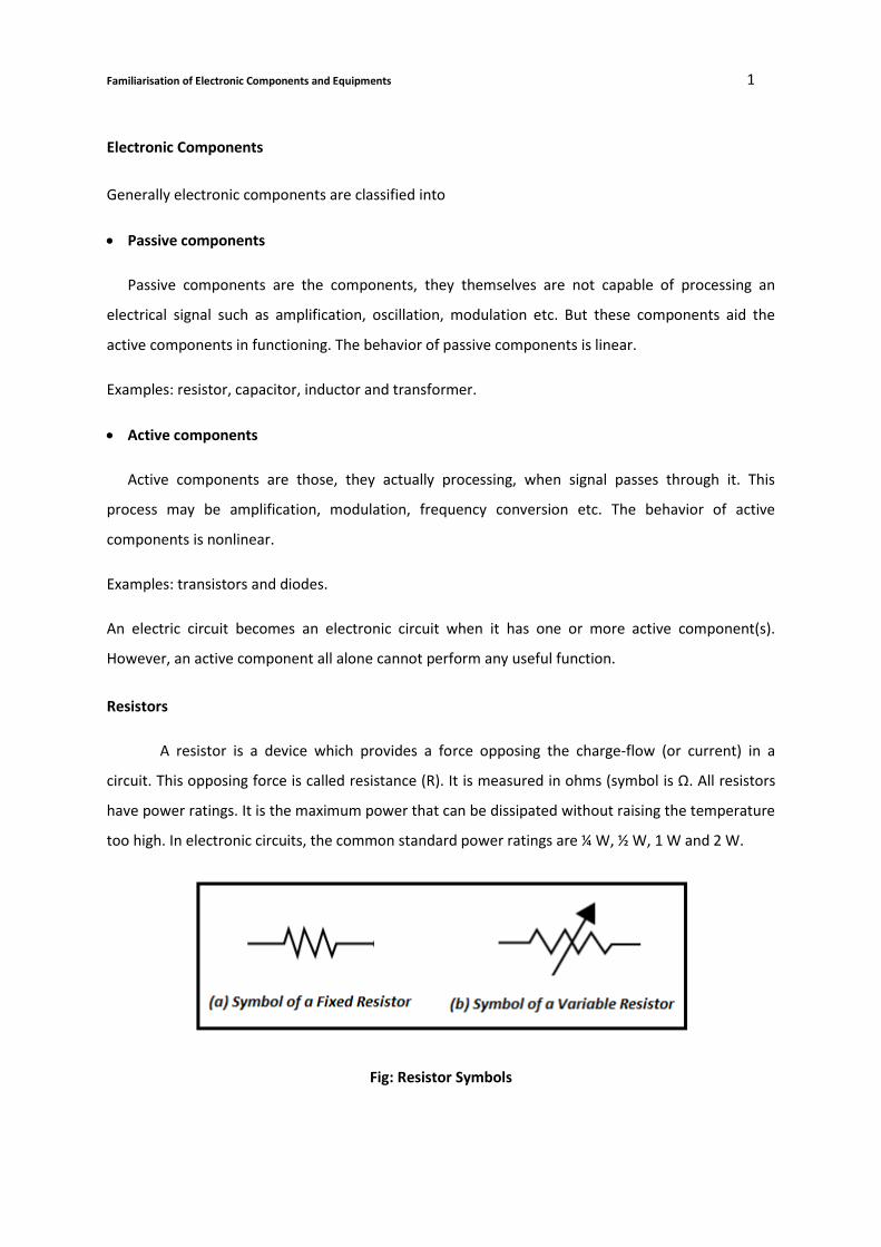
Resistors
A resistor is a device which provides a force opposing the charge-flow (or current) in a
circuit. This opposing force is called resistance (R). It is measured in ohms (symbol is Ω. All resistors
have power ratings. It is the maximum power that can be dissipated without raising the temperature
too high. In electronic circuits, the common standard power ratings are ¼ W, ½ W, 1 W and 2 W.
Fig: Resistor Symbols
Page 2
Familiarisation of Electronic Components and Equipments 2
There are two basic types of resistors.
1. Linear Resistors
2. Non Linear Resistors
1. Linear Resistors
Those resistors, which values change with the applied voltage and temperature, are called linear
resistors. In other words, a resistor, which current value is directly proportional to the applied
voltage is known as linear resistors.
Generally, there are two types of resistors which have linear properties.
a) Fixed Resistors b) Variable Resistors.
a) Fixed Resistors
As the name tells everything, fixed resistor is a resistor which has a specific value and we can’t
change the value of fixed resistors.
Types of Fixed resistors.
1. Carbon Composition Resistors
2. Wire Wound Resistors
3. Thin Film Resistors
4. Thick Film Resistors
Carbon Composition Resistor
These types of resistor are very commonly used low cost resistor. The construction of carbon
composition resistor is very simple. It is also commonly referred as carbon resistor. It is mainly made
of carbon clay composition covered with a plastic case. The lead of the resistor is made of tinned
copper. The main advantages of these resistors are that they are easily available in local market in
very low cost and they are very durable too. But the main disadvantage is that they are very much
temperature sensitive. These resistors are available in wide range of values. It is available in as low
as 1 Ω value and it is also available in as high as 22 Mega Ω value. The tolerance range in resistance
of carbon composition resistor is of ± 5 to ± 20 %. Such resistor has a tendency of electric noise due
to passage of electrical current from one carbon particle to other. Where low cost is the main
criteria of designing a circuit rather than it's performance, these resistors are normally used.
Page 3
Familiarisation of Electronic Components and Equipments 3
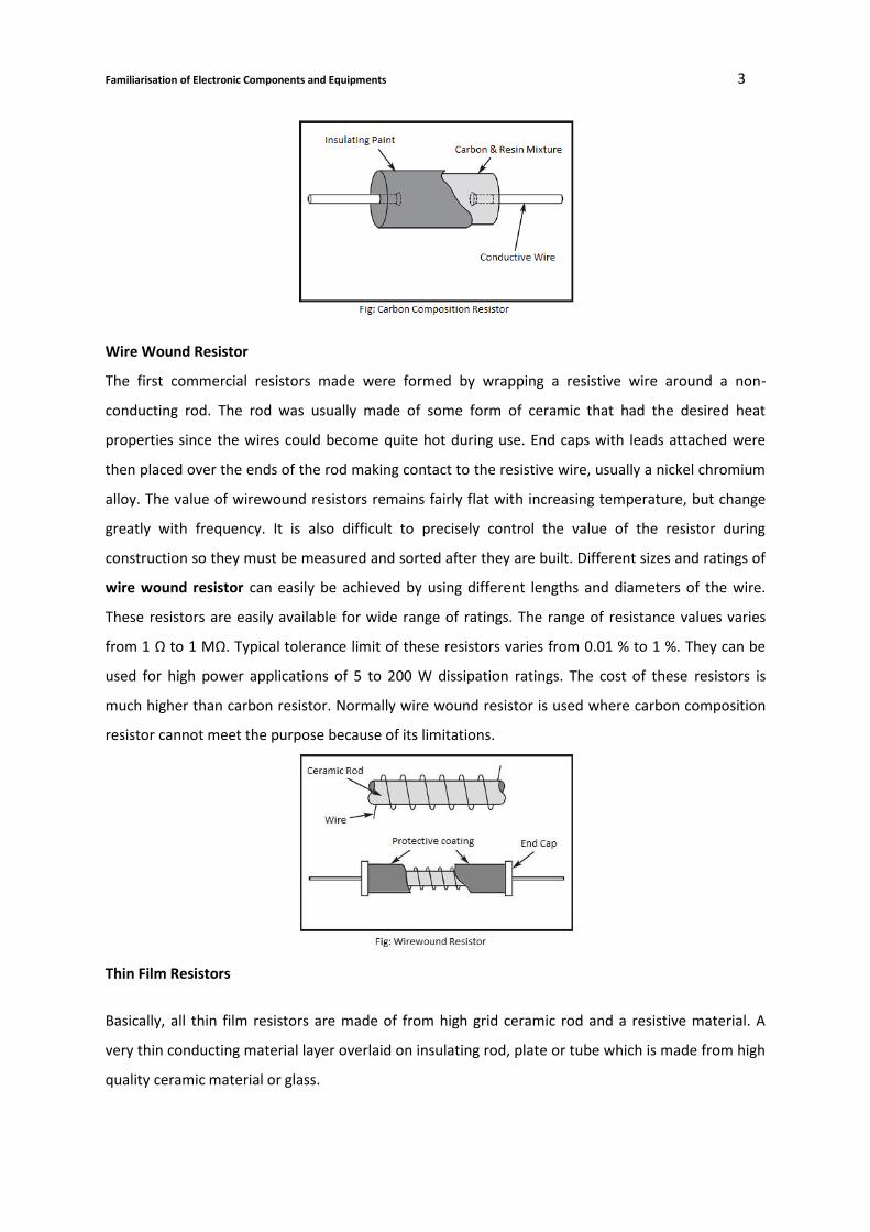
Wire Wound Resistor
The first commercial resistors made were formed by wrapping a resistive wire around a non-
conducting rod. The rod was usually made of some form of ceramic that had the desired heat
properties since the wires could become quite hot during use. End caps with leads attached were
then placed over the ends of the rod making contact to the resistive wire, usually a nickel chromium
alloy. The value of wirewound resistors remains fairly flat with increasing temperature, but change
greatly with frequency. It is also difficult to precisely control the value of the resistor during
construction so they must be measured and sorted after they are built. Different sizes and ratings of
wire wound resistor can easily be achieved by using different lengths and diameters of the wire.
These resistors are easily available for wide range of ratings. The range of resistance values varies
from 1 Ω to 1 MΩ. Typical tolerance limit of these resistors varies from 0.01 % to 1 %. They can be
used for high power applications of 5 to 200 W dissipation ratings. The cost of these resistors is
much higher than carbon resistor. Normally wire wound resistor is used where carbon composition
resistor cannot meet the purpose because of its limitations.
Thin Film Resistors
Basically, all thin film resistors are made of from high grid ceramic rod and a resistive material. A
very thin conducting material layer overlaid on insulating rod, plate or tube which is made from high
quality ceramic material or glass.
Page 4
Familiarisation of Electronic Components and Equipments 4
Thick Film Resistors
The production method of Thick film resistors is same like thin film resistors, but the difference is
that there is a thick film instead of a thin film or layer of resistive material around. That’s why it is
called Thick film resistors. b) Variable Resistors
When a resistor is constructed so its value can be adjusted, it is called a variable resistor. Figure
below shows the basic elements present in all variable resistors. First a resistive material is
deposited on a non-conducting base. Next, stationary contacts are connected to each end of the
resistive material. Finally, a moving contact or wiper is constructed to move along the resistive
material and tap off the desired resistance. There are many methods for constructing variable
resistors, but they all contain these three basic principles.
Fig: Variable Resistor
2. Non Linear Resistors
We know that, nonlinear resistors are those resistors, where the current flowing through it
does not change according to Ohm’s Law but, changes with change in temperature or applied
voltage.
In addition, if the flowing current through a resistor changes with change in body
temperature, then these kinds of resistors are called Thermisters. If the flowing current through a
resistor change with the applied voltages, then it is called a Varistors or VDR (Voltage Dependent
Resistors).
Following are the different types of Non Linear Resistors.
1.Thermisters
2.Varisters(VDR)
3. Photo Resistor or Photo Conductive Cell or LDR
Page 5
Familiarisation of Electronic Components and Equipments 5
Thermistors
Thermistors are thermally sensitive resistors whose prime function is to exhibit a large,
predictable and precise change in electrical resistance when subjected to a corresponding change in
body temperature. Thermisters are made from the cobalt, Nickel, Strontium and the metal oxides of
Manganese.Negative Temperature Coefficient (NTC) thermistors exhibit a decrease in electrical
resistance when subjected to an increase in body temperature and Positive Temperature Coefficient
(PTC) thermistors exhibit an increase in electrical resistance when subjected to an increase in body
temperature.
When thermistor is subjected to a temperature change,the resistance of the thermistor
changes.This change in resistance become a measure of the change in temperature when
calibrated.
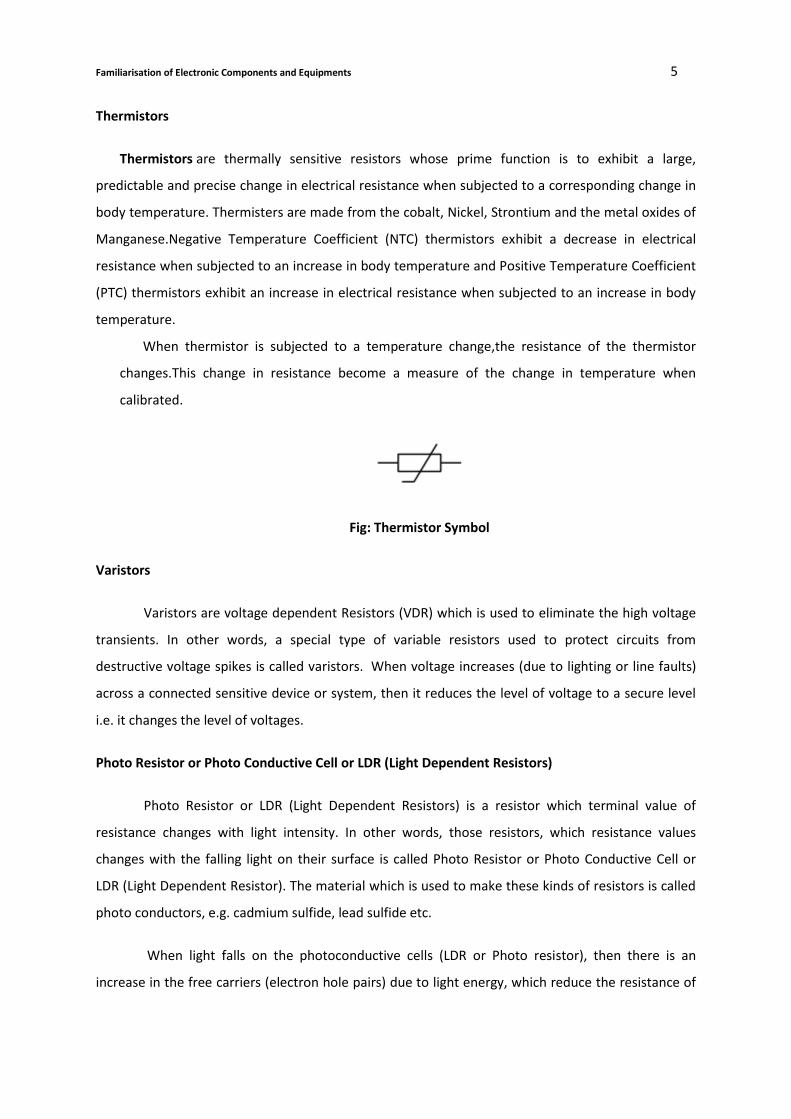
Fig: Thermistor Symbol
Varistors
Varistors are voltage dependent Resistors (VDR) which is used to eliminate the high voltage
transients. In other words, a special type of variable resistors used to protect circuits from
destructive voltage spikes is called varistors. When voltage increases (due to lighting or line faults)
across a connected sensitive device or system, then it reduces the level of voltage to a secure level
i.e. it changes the level of voltages.
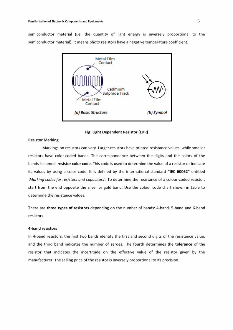
Photo Resistor or Photo Conductive Cell or LDR (Light Dependent Resistors)
Photo Resistor or LDR (Light Dependent Resistors) is a resistor which terminal value of
resistance changes with light intensity. In other words, those resistors, which resistance values
changes with the falling light on their surface is called Photo Resistor or Photo Conductive Cell or
LDR (Light Dependent Resistor). The material which is used to make these kinds of resistors is called
photo conductors, e.g. cadmium sulfide, lead sulfide etc.
When light falls on the photoconductive cells (LDR or Photo resistor), then there is an
increase in the free carriers (electron hole pairs) due to light energy, which reduce the resistance of
Page 6
Familiarisation of Electronic Components and Equipments 6
semiconductor material (i.e. the quantity of light energy is inversely proportional to the
semiconductor material). It means photo resistors have a negative temperature coefficient.
Fig: Light Dependent Resistor (LDR)
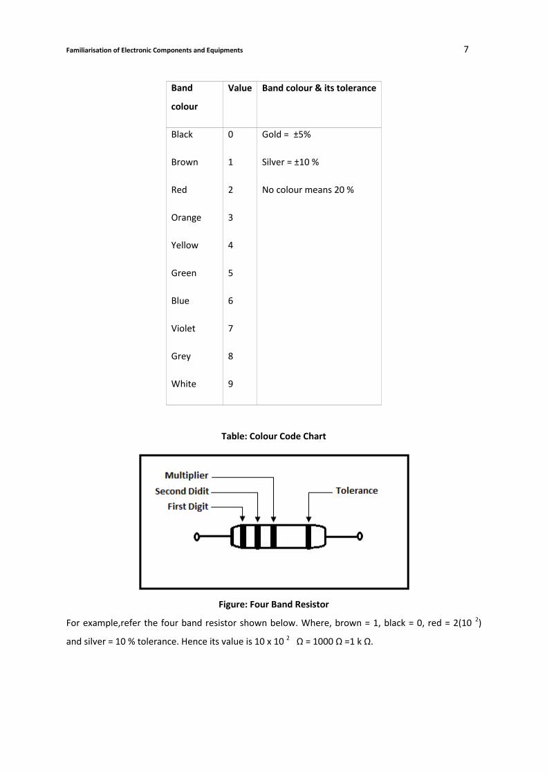
Resistor Marking
Markings on resistors can vary. Larger resistors have printed resistance values, while smaller
resistors have color-coded bands. The correspondence between the digits and the colors of the
bands is named resistor color code. This code is used to determine the value of a resistor or indicate
its values by using a color code. It is defined by the international standard “IEC 60062” entitled
‘Marking codes for resistors and capacitors’. To determine the resistance of a colour-coded resistor,
start from the end opposite the silver or gold band. Use the colour code chart shown in table to
determine the resistance values.
There are three types of resistors depending on the number of bands: 4-band, 5-band and 6-band
resistors.
4-band resistors
In 4-band resistors, the first two bands identify the first and second digits of the resistance value,
and the third band indicates the number of zeroes. The fourth determines the tolerance of the
resistor that indicates the incertitude on the effective value of the resistor given by the
manufacturer. The selling price of the resistor is inversely proportional to its precision.
Page 7
Familiarisation of Electronic Components and Equipments 7
Table: Colour Code Chart
Figure: Four Band Resistor
For example,refer the four band resistor shown below. Where, brown = 1, black = 0, red = 2(10 2)
and silver = 10 % tolerance. Hence its value is 10 x 10 2 Ω = 1000 Ω =1 k Ω.
Band
colour
Value Band colour & its tolerance
Black
Brown
Red
Orange
Yellow
Green
Blue
Violet
Grey
White
0
1
2
3
4
5
6
7
8
9
Gold = ±5%
Silver = ±10 %
No colour means 20 %
Page 8
Familiarisation of Electronic Components and Equipments 8
Capacitors
The Capacitor, sometimes referred to as Condenser, is a simple passive element that is used to
‘store electricity’. The capacitor is a component which has the ability or ‘capacity’ to store energy in
the form of an electrical charge producing a potential difference across its plates, much like a small
rechargeable battery.
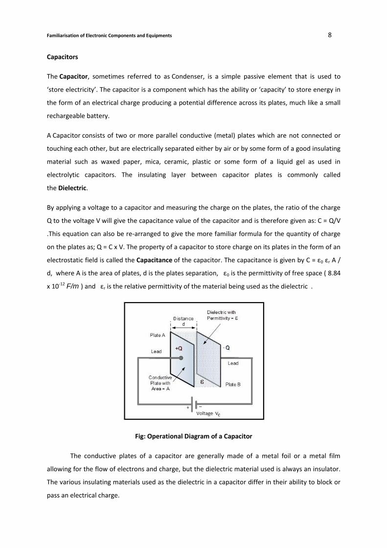
A Capacitor consists of two or more parallel conductive (metal) plates which are not connected or
touching each other, but are electrically separated either by air or by some form of a good insulating
material such as waxed paper, mica, ceramic, plastic or some form of a liquid gel as used in
electrolytic capacitors. The insulating layer between capacitor plates is commonly called
the Dielectric.
By applying a voltage to a capacitor and measuring the charge on the plates, the ratio of the charge
Q to the voltage V will give the capacitance value of the capacitor and is therefore given as: C = Q/V
.This equation can also be re-arranged to give the more familiar formula for the quantity of charge
on the plates as; Q = C x V. The property of a capacitor to store charge on its plates in the form of an
electrostatic field is called the Capacitance of the capacitor. The capacitance is given by C = ε0 εr A /
d, where A is the area of plates, d is the plates separation, ε0 is the permittivity of free space ( 8.84
x 10-12 F/m ) and εr is the relative permittivity of the material being used as the dielectric .
Fig: Operational Diagram of a Capacitor
The conductive plates of a capacitor are generally made of a metal foil or a metal film
allowing for the flow of electrons and charge, but the dielectric material used is always an insulator.
The various insulating materials used as the dielectric in a capacitor differ in their ability to block or
pass an electrical charge.
Page 9
Familiarisation of Electronic Components and Equipments 9
This dielectric material can be made from a number of insulating materials or combinations
of these materials with the most common types used being: air, paper, polyester, polypropylene,
Mylar, ceramic, glass, oil, or a variety of other materials.
Capacitance is defined as being that a capacitor has the capacitance of One Farad when a charge
of One Coulomb is stored on the plates by a voltage of One volt. Capacitance, C is always positive
and has no negative units. However, the Farad is a very large unit of measurement to use on its own
so sub-multiples of the Farad are generally used such as micro-farads, nano-farads and pico-farads.
Microfarad (μF) 1μF = 10-6 F
Nanofarad (nF) 1nF = 10-9 F
Picofarad (pF) 1pF = 10-12 F
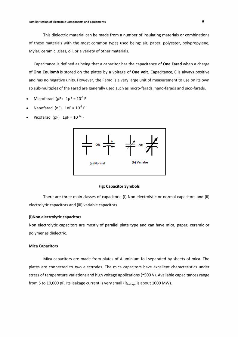
Fig: Capacitor Symbols
There are three main classes of capacitors: (i) Non electrolytic or normal capacitors and (ii)
electrolytic capacitors and (iii) variable capacitors.
(i)Non electrolytic capacitors
Non electrolytic capacitors are mostly of parallel plate type and can have mica, paper, ceramic or
polymer as dielectric.
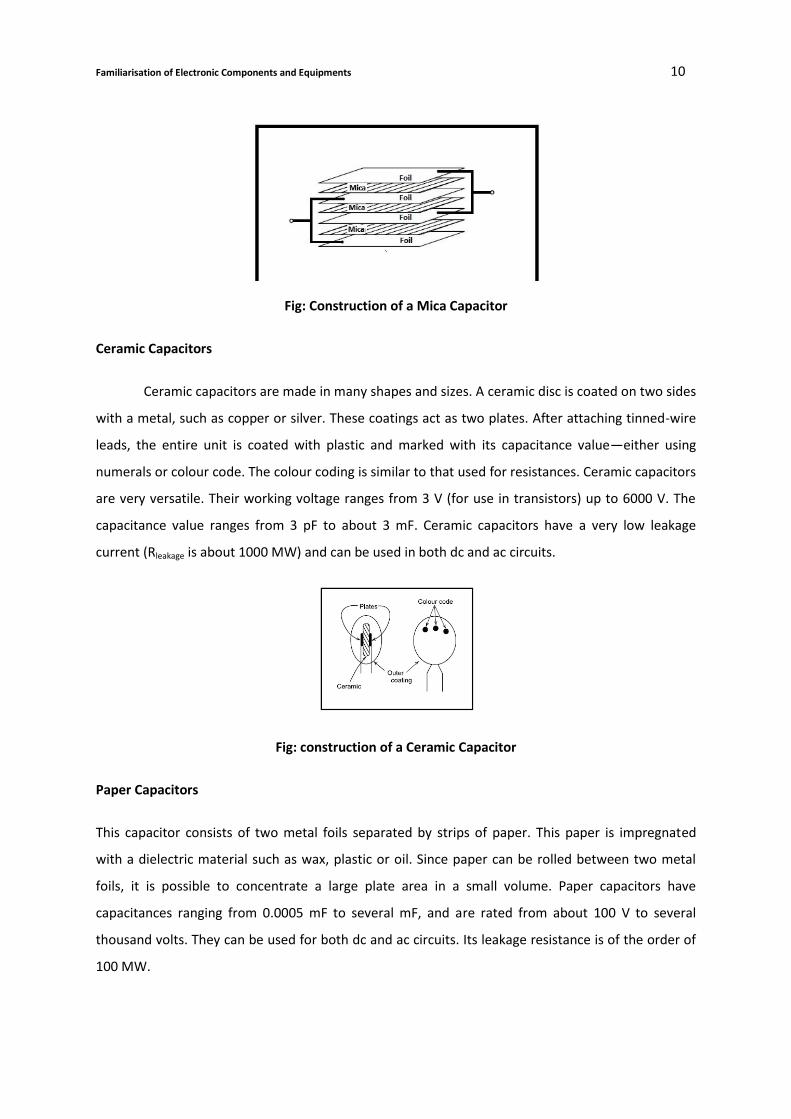
Mica Capacitors
Mica capacitors are made from plates of Aluminium foil separated by sheets of mica. The
plates are connected to two electrodes. The mica capacitors have excellent characteristics under
stress of temperature variations and high voltage applications (~500 V). Available capacitances range
from 5 to 10,000 pF. Its leakage current is very small (Rleakage is about 1000 MW).
Page 10
Familiarisation of Electronic Components and Equipments 10
Fig: Construction of a Mica Capacitor
Ceramic Capacitors
Ceramic capacitors are made in many shapes and sizes. A ceramic disc is coated on two sides
with a metal, such as copper or silver. These coatings act as two plates. After attaching tinned-wire
leads, the entire unit is coated with plastic and marked with its capacitance value—either using
numerals or colour code. The colour coding is similar to that used for resistances. Ceramic capacitors
are very versatile. Their working voltage ranges from 3 V (for use in transistors) up to 6000 V. The
capacitance value ranges from 3 pF to about 3 mF. Ceramic capacitors have a very low leakage
current (Rleakage is about 1000 MW) and can be used in both dc and ac circuits.
Fig: construction of a Ceramic Capacitor
Paper Capacitors
This capacitor consists of two metal foils separated by strips of paper. This paper is impregnated
with a dielectric material such as wax, plastic or oil. Since paper can be rolled between two metal
foils, it is possible to concentrate a large plate area in a small volume. Paper capacitors have
capacitances ranging from 0.0005 mF to several mF, and are rated from about 100 V to several
thousand volts. They can be used for both dc and ac circuits. Its leakage resistance is of the order of
100 MW.
Page 11
Familiarisation of Electronic Components and Equipments 11
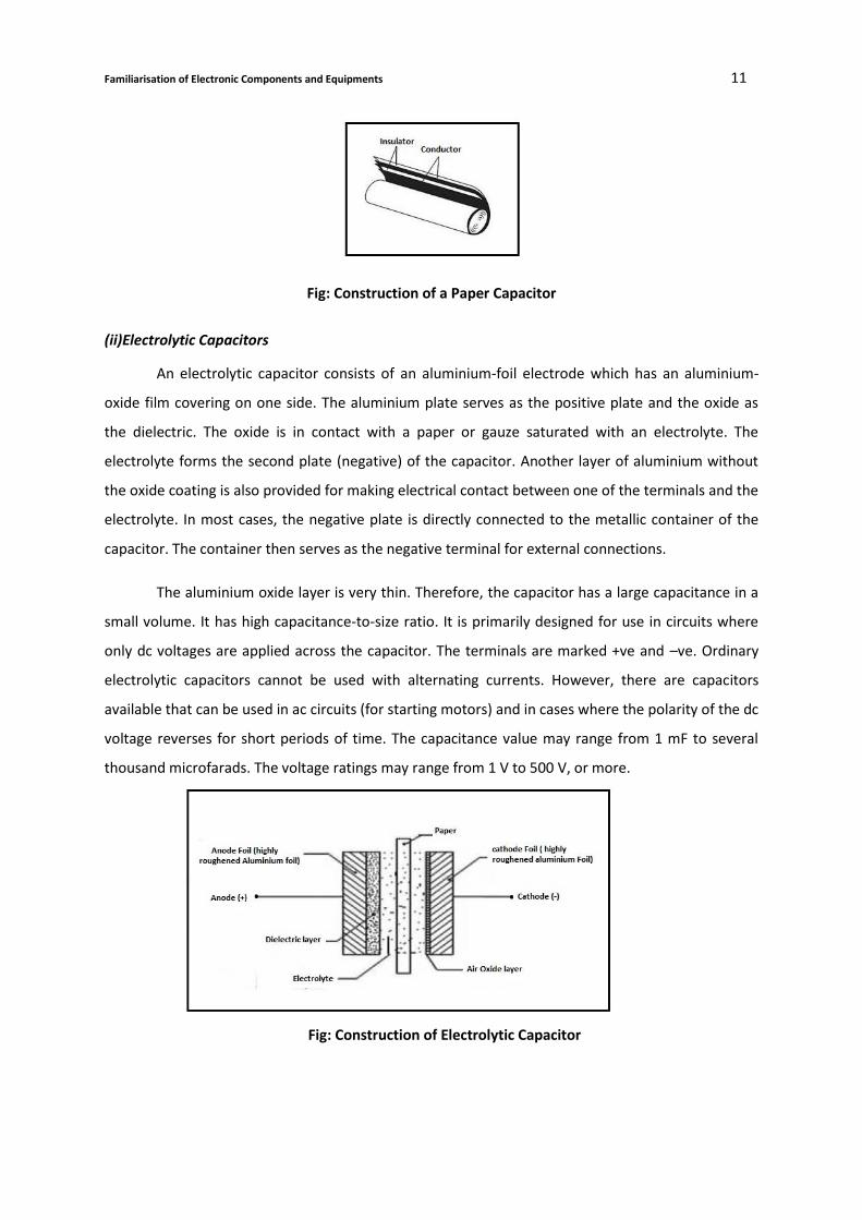
Fig: Construction of a Paper Capacitor
(ii)Electrolytic Capacitors
An electrolytic capacitor consists of an aluminium-foil electrode which has an aluminium-
oxide film covering on one side. The aluminium plate serves as the positive plate and the oxide as
the dielectric. The oxide is in contact with a paper or gauze saturated with an electrolyte. The
electrolyte forms the second plate (negative) of the capacitor. Another layer of aluminium without
the oxide coating is also provided for making electrical contact between one of the terminals and the
electrolyte. In most cases, the negative plate is directly connected to the metallic container of the
capacitor. The container then serves as the negative terminal for external connections.
The aluminium oxide layer is very thin. Therefore, the capacitor has a large capacitance in a
small volume. It has high capacitance-to-size ratio. It is primarily designed for use in circuits where
only dc voltages are applied across the capacitor. The terminals are marked +ve and –ve. Ordinary
electrolytic capacitors cannot be used with alternating currents. However, there are capacitors
available that can be used in ac circuits (for starting motors) and in cases where the polarity of the dc
voltage reverses for short periods of time. The capacitance value may range from 1 mF to several
thousand microfarads. The voltage ratings may range from 1 V to 500 V, or more.
Fig: Construction of Electrolytic Capacitor
Page 12
Familiarisation of Electronic Components and Equipments 12
Electrolytic Capacitors are generally used in DC power supply circuits due to their large
capacitance’s and small size to help reduce the ripple voltage or for coupling and decoupling
applications. One main disadvantage of electrolytic capacitors is their relatively low voltage rating
and due to the polarisation of electrolytic capacitors, it follows then that they must not be used on
AC supplies. Electrolytic’s generally come in two basic forms; Aluminium Electrolytic
Capacitors and Tantalum Electrolytic Capacitors.
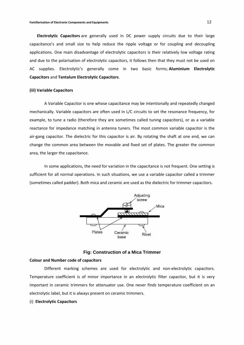
(iii) Variable Capacitors
A Variable Capacitor is one whose capacitance may be intentionally and repeatedly changed
mechanically. Variable capacitors are often used in L/C circuits to set the resonance frequency, for
example, to tune a radio (therefore they are sometimes called tuning capacitors), or as a variable
reactance for impedance matching in antenna tuners. The most common variable capacitor is the
air-gang capacitor. The dielectric for this capacitor is air. By rotating the shaft at one end, we can
change the common area between the movable and fixed set of plates. The greater the common
area, the larger the capacitance.
In some applications, the need for variation in the capacitance is not frequent. One setting is
sufficient for all normal operations. In such situations, we use a variable capacitor called a trimmer
(sometimes called padder). Both mica and ceramic are used as the dielectric for trimmer capacitors.
Fig: Construction of a Mica Trimmer
Colour and Number code of capacitors
Different marking schemes are used for electrolytic and non-electrolytic capacitors.
Temperature coefficient is of minor importance in an electrolytic filter capacitor, but it is very
important in ceramic trimmers for attenuator use. One never finds temperature coefficient on an
electrolytic label, but it is always present on ceramic trimmers.
(i) Electrolytic Capacitors
Page 13
Familiarisation of Electronic Components and Equipments 13
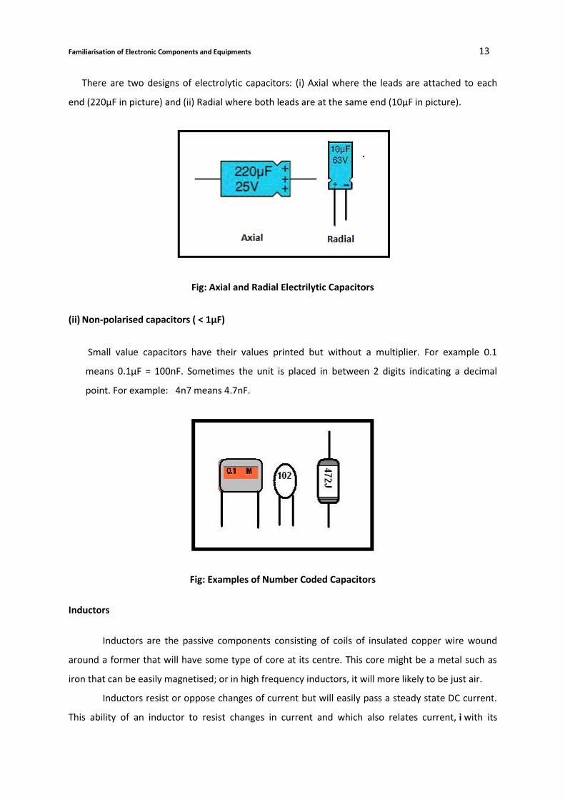
There are two designs of electrolytic capacitors: (i) Axial where the leads are attached to each
end (220µF in picture) and (ii) Radial where both leads are at the same end (10µF in picture).
Fig: Axial and Radial Electrilytic Capacitors
(ii) Non-polarised capacitors ( < 1µF)
Small value capacitors have their values printed but without a multiplier. For example 0.1
means 0.1µF = 100nF. Sometimes the unit is placed in between 2 digits indicating a decimal
point. For example: 4n7 means 4.7nF.
Fig: Examples of Number Coded Capacitors
Inductors
Inductors are the passive components consisting of coils of insulated copper wire wound
around a former that will have some type of core at its centre. This core might be a metal such as
iron that can be easily magnetised; or in high frequency inductors, it will more likely to be just air.
Inductors resist or oppose changes of current but will easily pass a steady state DC current.
This ability of an inductor to resist changes in current and which also relates current, i with its
Page 14
Familiarisation of Electronic Components and Equipments 14
magnetic flux linkage, Nφ as a constant of proportionality is called Inductance which is given the
symbol L . Inductance of a coil is measured in Henry’s. This name comes from an outstanding
scientist by the name of Joseph Henry who studied coils and their properties in the early days of
electronics. One Henry is the amount of inductance required to produce an e.m.f. of 1 volt in a
conductor when the current in the conductor changes at the rate of 1 Ampere per second. Typically,
milli Henry’s or even micro Henry’s are used to measure inductance. Large power transformers in
power substation may have 1000 Henry’s or more of inductance.
Fig: Inductor Basics
Transformers
Transformer is a static device which transforms electrical energy from one circuit to another
without any direct electrical connection and with the help of mutual induction between two
windings. It transforms power from one circuit to another without changing its frequency but may
be in different voltage level. Transformers are commonly used in applications which require the
conversion of AC voltage from one voltage level to another.
There are two broad categories of transformers: electronic transformers, which operate at
very low power levels, and power transformers, which process thousands of watts of power.
Electronic transformers are used in consumer electronic equipment like television sets, CD players,
personal computers, and many other devices, to reduce the level of voltage from 220V (available
from the AC mains) to the desired level at which the device operates. Power transformers are used
in power generation, transmission and distribution systems to raise or lower the level of voltage to
the desired levels. The basic principle of operation of both types of transformers is the same.
Page 15
Familiarisation of Electronic Components and Equipments 15
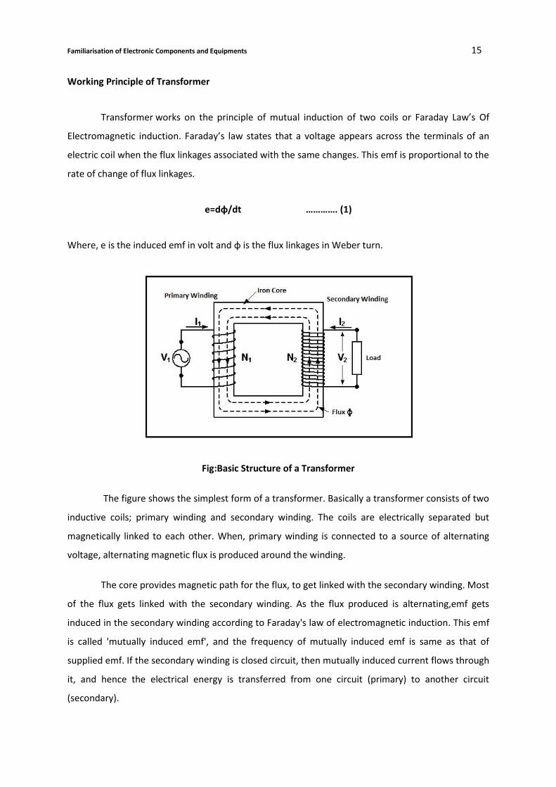
Working Principle of Transformer
Transformer works on the principle of mutual induction of two coils or Faraday Law’s Of
Electromagnetic induction. Faraday’s law states that a voltage appears across the terminals of an
electric coil when the flux linkages associated with the same changes. This emf is proportional to the
rate of change of flux linkages.
e=dφ/dt …………. (1)
Where, e is the induced emf in volt and φ is the flux linkages in Weber turn.
Fig:Basic Structure of a Transformer
The figure shows the simplest form of a transformer. Basically a transformer consists of two
inductive coils; primary winding and secondary winding. The coils are electrically separated but
magnetically linked to each other. When, primary winding is connected to a source of alternating
voltage, alternating magnetic flux is produced around the winding.
The core provides magnetic path for the flux, to get linked with the secondary winding. Most
of the flux gets linked with the secondary winding. As the flux produced is alternating,emf gets
induced in the secondary winding according to Faraday's law of electromagnetic induction. This emf
is called 'mutually induced emf', and the frequency of mutually induced emf is same as that of
supplied emf. If the secondary winding is closed circuit, then mutually induced current flows through
it, and hence the electrical energy is transferred from one circuit (primary) to another circuit
(secondary).
Page 16
Familiarisation of Electronic Components and Equipments 16
Types of Transformers
The transformers are classified based on voltage levels, design, Core medium used,winding
arrangements and the type of cooling employed.
Transformers based on voltage levels
The transformers are classified as step-up and step-down transformers as the voltage ratios from
primary to secondary. These are widely used transformer types for all the applications. Here the
important thing to remember is that there will not be any difference in primary power and
secondary power. That means if the voltage is high at secondary side then the current drawn from
the secondary will low so that the power will be same. Same as in the reverse case when the voltage
is low the current drawn will be high.
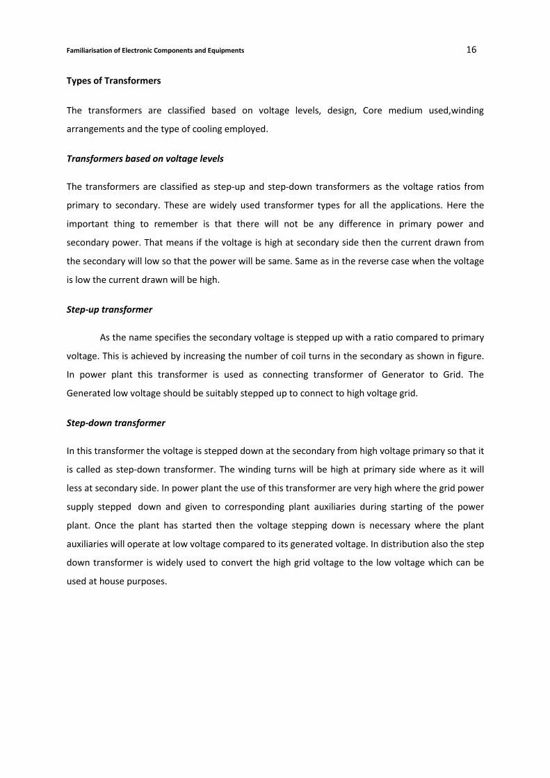
Step-up transformer
As the name specifies the secondary voltage is stepped up with a ratio compared to primary
voltage. This is achieved by increasing the number of coil turns in the secondary as shown in figure.
In power plant this transformer is used as connecting transformer of Generator to Grid. The
Generated low voltage should be suitably stepped up to connect to high voltage grid.
Step-down transformer
In this transformer the voltage is stepped down at the secondary from high voltage primary so that it
is called as step-down transformer. The winding turns will be high at primary side where as it will
less at secondary side. In power plant the use of this transformer are very high where the grid power
supply stepped down and given to corresponding plant auxiliaries during starting of the power
plant. Once the plant has started then the voltage stepping down is necessary where the plant
auxiliaries will operate at low voltage compared to its generated voltage. In distribution also the step
down transformer is widely used to convert the high grid voltage to the low voltage which can be
used at house purposes.
Page 17
Familiarisation of Electronic Components and Equipments 17
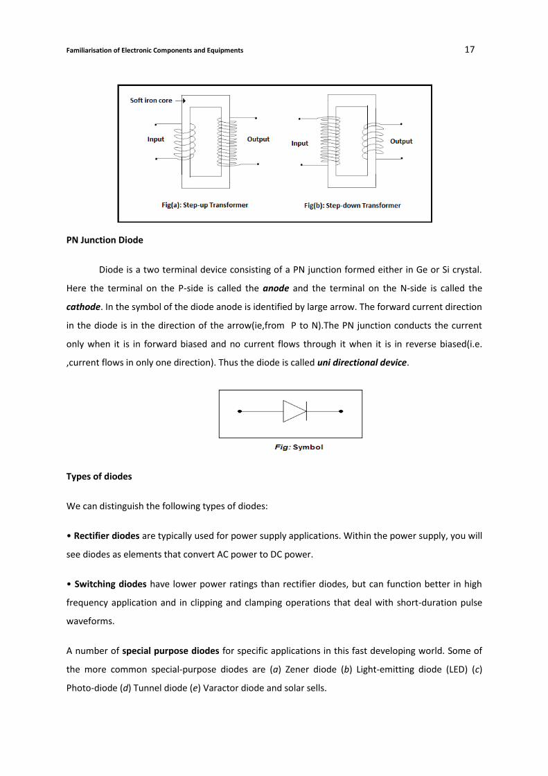
PN Junction Diode
Diode is a two terminal device consisting of a PN junction formed either in Ge or Si crystal.
Here the terminal on the P-side is called the anode and the terminal on the N-side is called the
cathode. In the symbol of the diode anode is identified by large arrow. The forward current direction
in the diode is in the direction of the arrow(ie,from P to N).The PN junction conducts the current
only when it is in forward biased and no current flows through it when it is in reverse biased(i.e.
,current flows in only one direction). Thus the diode is called uni directional device.
Types of diodes
We can distinguish the following types of diodes:
• Rectifier diodes are typically used for power supply applications. Within the power supply, you will
see diodes as elements that convert AC power to DC power.
• Switching diodes have lower power ratings than rectifier diodes, but can function better in high
frequency application and in clipping and clamping operations that deal with short-duration pulse
waveforms.
A number of special purpose diodes for specific applications in this fast developing world. Some of
the more common special-purpose diodes are (a) Zener diode (b) Light-emitting diode (LED) (c)
Photo-diode (d) Tunnel diode (e) Varactor diode and solar sells.
Page 18
Familiarisation of Electronic Components and Equipments 18
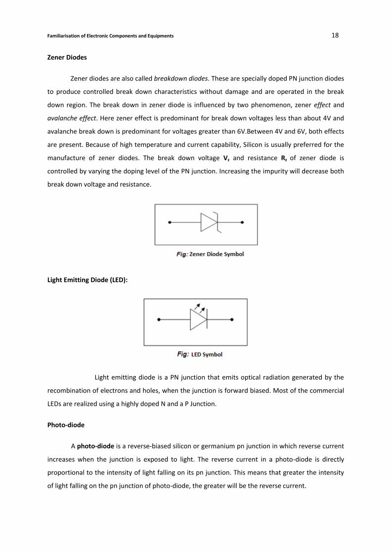
Zener Diodes
Zener diodes are also called breakdown diodes. These are specially doped PN junction diodes
to produce controlled break down characteristics without damage and are operated in the break
down region. The break down in zener diode is influenced by two phenomenon, zener effect and
avalanche effect. Here zener effect is predominant for break down voltages less than about 4V and
avalanche break down is predominant for voltages greater than 6V.Between 4V and 6V, both effects
are present. Because of high temperature and current capability, Silicon is usually preferred for the
manufacture of zener diodes. The break down voltage Vz and resistance Rz of zener diode is
controlled by varying the doping level of the PN junction. Increasing the impurity will decrease both
break down voltage and resistance.
Light Emitting Diode (LED):
Light emitting diode is a PN junction that emits optical radiation generated by the
recombination of electrons and holes, when the junction is forward biased. Most of the commercial
LEDs are realized using a highly doped N and a P Junction.
Photo-diode
A photo-diode is a reverse-biased silicon or germanium pn junction in which reverse current
increases when the junction is exposed to light. The reverse current in a photo-diode is directly
proportional to the intensity of light falling on its pn junction. This means that greater the intensity
of light falling on the pn junction of photo-diode, the greater will be the reverse current.
Page 19
Familiarisation of Electronic Components and Equipments 19
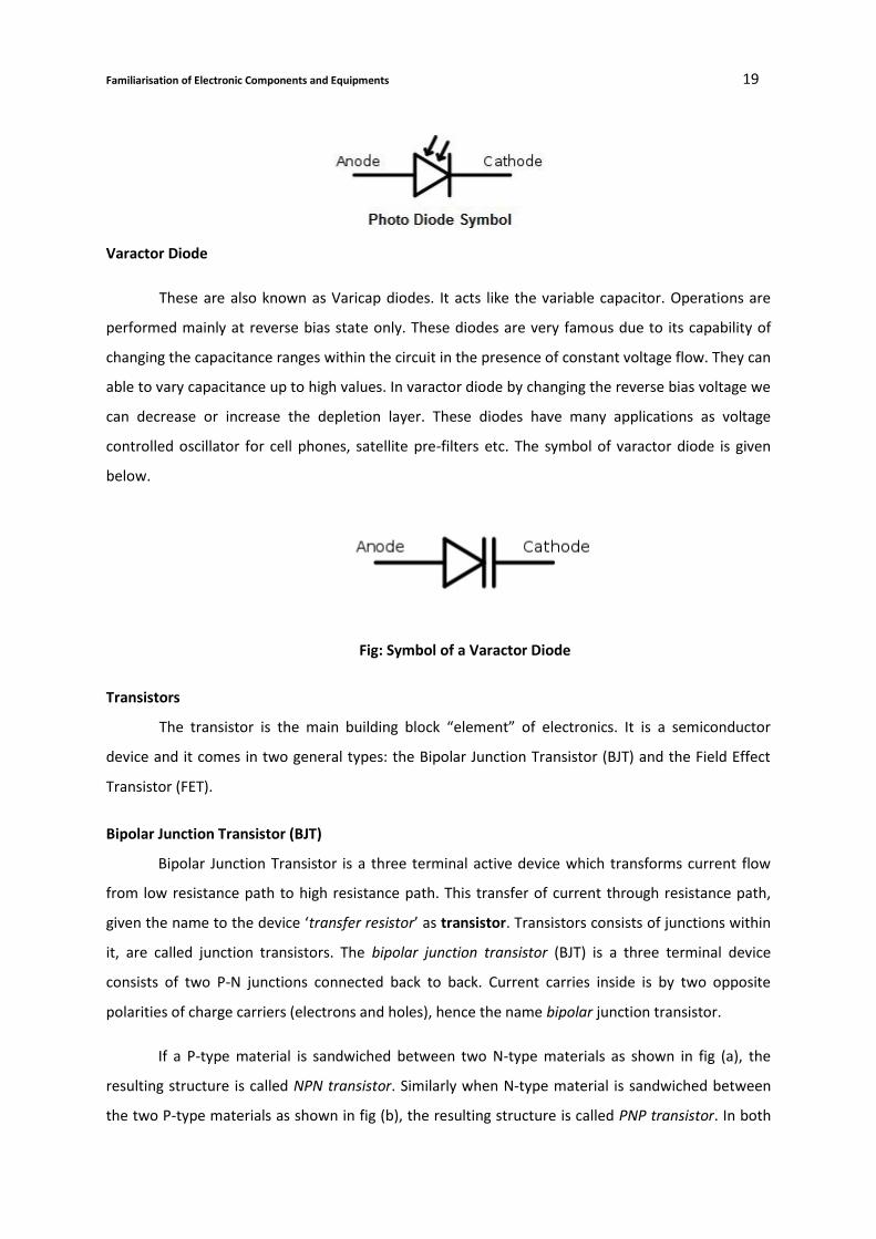
Varactor Diode
These are also known as Varicap diodes. It acts like the variable capacitor. Operations are
performed mainly at reverse bias state only. These diodes are very famous due to its capability of
changing the capacitance ranges within the circuit in the presence of constant voltage flow. They can
able to vary capacitance up to high values. In varactor diode by changing the reverse bias voltage we
can decrease or increase the depletion layer. These diodes have many applications as voltage
controlled oscillator for cell phones, satellite pre-filters etc. The symbol of varactor diode is given
below.
Fig: Symbol of a Varactor Diode
Transistors
The transistor is the main building block “element” of electronics. It is a semiconductor
device and it comes in two general types: the Bipolar Junction Transistor (BJT) and the Field Effect
Transistor (FET).
Bipolar Junction Transistor (BJT)
Bipolar Junction Transistor is a three terminal active device which transforms current flow
from low resistance path to high resistance path. This transfer of current through resistance path,
given the name to the device ‘transfer resistor’ as transistor. Transistors consists of junctions within
it, are called junction transistors. The bipolar junction transistor (BJT) is a three terminal device
consists of two P-N junctions connected back to back. Current carries inside is by two opposite
polarities of charge carriers (electrons and holes), hence the name bipolar junction transistor.
If a P-type material is sandwiched between two N-type materials as shown in fig (a), the
resulting structure is called NPN transistor. Similarly when N-type material is sandwiched between
the two P-type materials as shown in fig (b), the resulting structure is called PNP transistor. In both
Page 20
Familiarisation of Electronic Components and Equipments 20
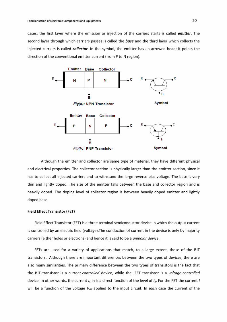
cases, the first layer where the emission or injection of the carriers starts is called emitter. The
second layer through which carriers passes is called the base and the third layer which collects the
injected carriers is called collector. In the symbol, the emitter has an arrowed head; it points the
direction of the conventional emitter current (from P to N region).
Although the emitter and collector are same type of material, they have different physical
and electrical properties. The collector section is physically larger than the emitter section, since it
has to collect all injected carriers and to withstand the large reverse bias voltage. The base is very
thin and lightly doped. The size of the emitter falls between the base and collector region and is
heavily doped. The doping level of collector region is between heavily doped emitter and lightly
doped base.
Field Effect Transistor (FET)
Field Effect Transistor (FET) is a three terminal semiconductor device in which the output current
is controlled by an electric field (voltage).The conduction of current in the device is only by majority
carriers (either holes or electrons) and hence it is said to be a unipolar device.
FETs are used for a variety of applications that match, to a large extent, those of the BJT
transistors. Although there are important differences between the two types of devices, there are
also many similarities. The primary difference between the two types of transistors is the fact that
the BJT transistor is a current-controlled device, while the JFET transistor is a voltage-controlled
device. In other words, the current IC in is a direct function of the level of IB. For the FET the current I
will be a function of the voltage VGS applied to the input circuit. In each case the current of the
Page 21
Familiarisation of Electronic Components and Equipments 21
output circuit is being controlled by a parameter of the input circuit—in one case a current level and
in the other an applied voltage. Just as there are npn and pnp bipolar transistors, there are n-channel
and p-channel field-effect transistors. BJTs have two main drawbacks namely low input impedance
because of forward biased emitter junction and considerable noise level. Both of these drawbacks
have been overcome, to a great extent in the field effect transistor (FET).
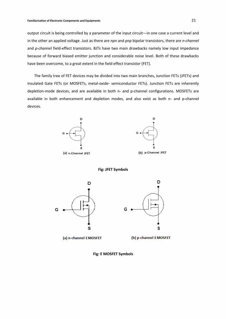
The family tree of FET devices may be divided into two main branches, Junction FETs (JFETs) and
Insulated Gate FETs (or MOSFETs, metal-oxide- semiconductor FETs). Junction FETs are inherently
depletion-mode devices, and are available in both n- and p-channel configurations. MOSFETs are
available in both enhancement and depletion modes, and also exist as both n- and p-channel
devices.
Fig: JFET Symbols
Fig: E MOSFET Symbols
Page 22
Familiarisation of Electronic Components and Equipments 22
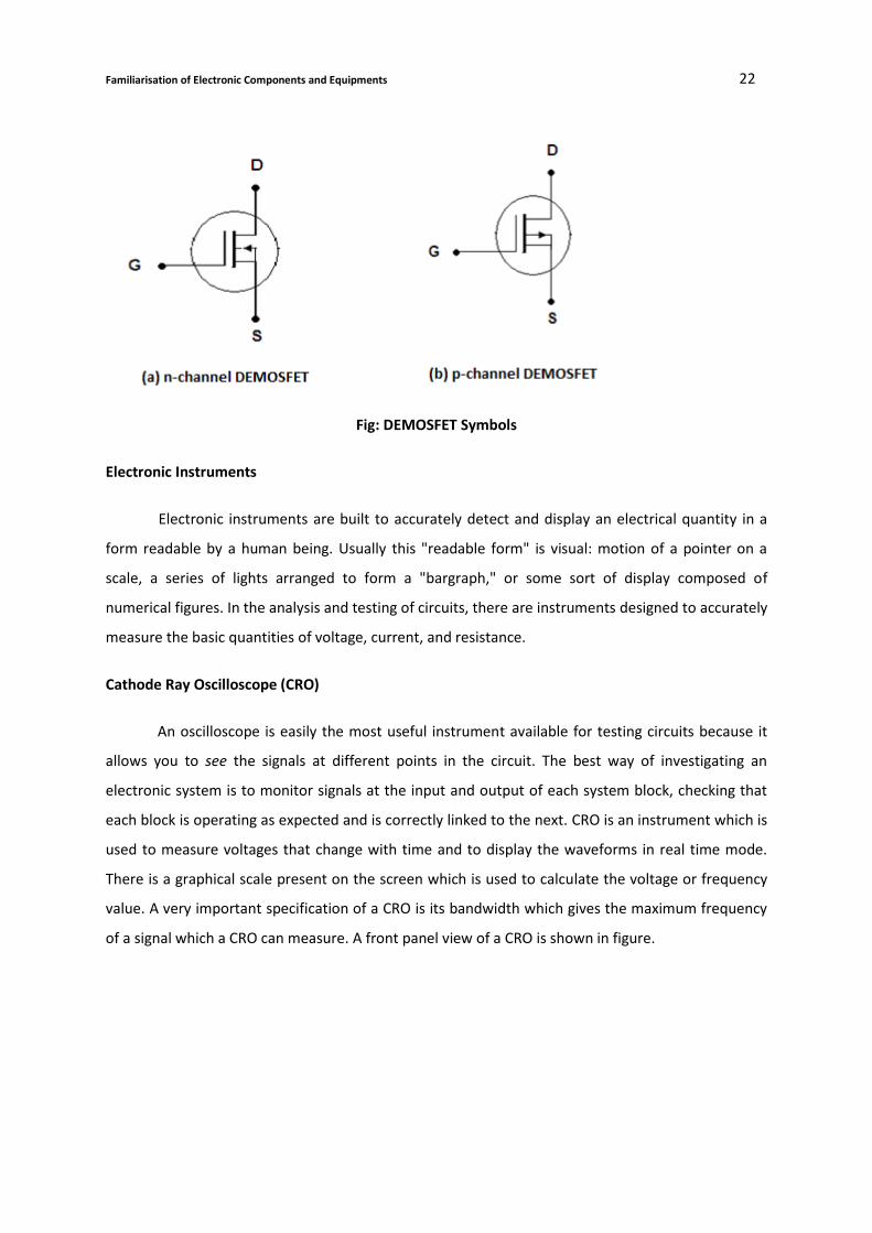
Fig: DEMOSFET Symbols
Electronic Instruments
Electronic instruments are built to accurately detect and display an electrical quantity in a
form readable by a human being. Usually this "readable form" is visual: motion of a pointer on a
scale, a series of lights arranged to form a "bargraph," or some sort of display composed of
numerical figures. In the analysis and testing of circuits, there are instruments designed to accurately
measure the basic quantities of voltage, current, and resistance.
Cathode Ray Oscilloscope (CRO)
An oscilloscope is easily the most useful instrument available for testing circuits because it
allows you to see the signals at different points in the circuit. The best way of investigating an
electronic system is to monitor signals at the input and output of each system block, checking that
each block is operating as expected and is correctly linked to the next. CRO is an instrument which is
used to measure voltages that change with time and to display the waveforms in real time mode.
There is a graphical scale present on the screen which is used to calculate the voltage or frequency
value. A very important specification of a CRO is its bandwidth which gives the maximum frequency
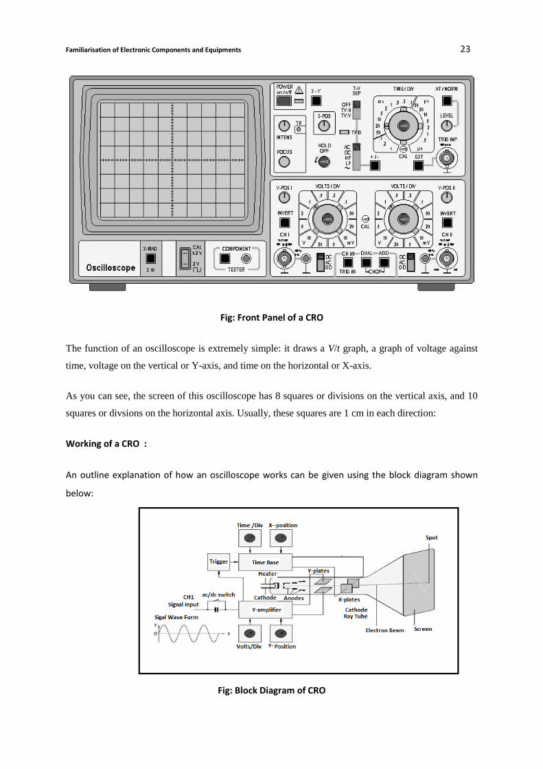
of a signal which a CRO can measure. A front panel view of a CRO is shown in figure.
Page 23
Familiarisation of Electronic Components and Equipments 23
Fig: Front Panel of a CRO
The function of an oscilloscope is extremely simple: it draws a V/t graph, a graph of voltage against
time, voltage on the vertical or Y-axis, and time on the horizontal or X-axis.
As you can see, the screen of this oscilloscope has 8 squares or divisions on the vertical axis, and 10
squares or divsions on the horizontal axis. Usually, these squares are 1 cm in each direction:
Working of a CRO :
An outline explanation of how an oscilloscope works can be given using the block diagram shown
below:
Fig: Block Diagram of CRO
Page 24
Familiarisation of Electronic Components and Equipments 24
A simple cathode ray oscilloscope consists of a cathode ray tube, a vertical amplifier, a time
base, a horizontal amplifier,a trigger circuit and a power supply.
Like a televison screen, the screen of an oscilloscope consists of a cathode ray tube.
Although the size and shape are different, the operating principle is the same. Inside the tube is a
vacuum. The electron beam emitted by the heated cathode at the rear end of the tube is
accelerated and focused by one or more anodes, and strikes the front of the tube, producing a bright
spot on the phosphorescent screen.
The electron beam is bent, or deflected, by voltages applied to two sets of plates fixed in the
tube. The horizontal deflection plates, or X-plates produce side to side movement. As you can see,
they are linked to a system block called the time base. This produces a sawtooth waveform. During
the rising phase of the sawtooth, the spot is driven at a uniform rate from left to right across the
front of the screen. During the falling phase, the electron beam returns rapidly from right ot left, but
the spot is 'blanked out' so that nothing appears on the screen.In this way, the time base generates
the X-axis of the V/t graph.
The slope of the rising phase varies with the frequency of the sawtooth and can be adjusted,
using the TIME/DIV control, to change the scale of the X-axis. Dividing the oscilloscope screen into
squares allows the horizontal scale to be expressed in seconds, milliseconds or microseconds per
division (s/DIV, ms/DIV, µs/DIV). Alternatively, if the squares are 1 cm apart, the scale may be given
as s/cm, ms/cm or µs/cm.
The signal to be displayed is connected to the input. The AC/DC switch is usually kept in the
DC position (switch closed) so that there is a direct connection to the Y-amplifier. In the AC position
(switch open) a capacitor is placed in the signal path. The capacitor blocks DC signals but allows AC
signals to pass.
The Y-amplifier is linked in turn to a pair of Y-plates so that it provides the Y-axis of the the
V/t graph. The overall gain of the Y-amplifier can be adjusted, using the VOLTS/DIV control, so that
the resulting display is neither too small or too large, but fits the screen and can be seen clearly. The
vertical scale is usually given in V/DIV or mV/DIV.
The trigger circuit is used to delay the time base waveform so that the same section of the
input signal is displayed on the screen each time the spot moves across. The effect of this is to give a
stable picture on the oscilloscope screen, making it easier to measure and interpret the signal.
Page 25
Familiarisation of Electronic Components and Equipments 25
Changing the scales of the X-axis and Y-axis allows many different signals to be displayed.
Sometimes, it is also useful to be able to change the positions of the axes. This is possible using the
X-POS and Y-POS controls. For example, with no signal applied, the normal trace is a straight line
across the centre of the screen. Adjusting Y-POS allows the zero level on the Y-axis to be changed,
moving the whole trace up or down on the screen to give an effective display of signals like pulse
waveforms which do not alternate between positive and negative values.
Front-panel controls
Intensity. This knob controls the brightness of the trace by adjusting the number of electrons
emerging from the gun.
Focus. This control is for making the trace on the screen sharper. It is connected to the anode of the
electron gun whose voltage collimates the electron beam.
Vertical Position & Horizontal Position. Through these controls the beam can be positioned at
variable vertical or horizontal positions as desired. These knobs apply a dc voltage to the vertical and
horizontal deflection plates.
Volt / Division. This control is used to control the voltage sensitivity. This is internally connected to
an attenuator of the vertical system. It determines the voltage required by the vertical plates to
deflect the beam vertically by one division.
Time / Division. This determines the time taken for the spot to move horizontally across one division
of the screen when the sweep is generated by triggering process. The signal which is fed to the
vertical deflection plates provides the triggering to the waveform. Each position of the time/ div
knob is applicable for a particular frequency. This determines the horizontal sensitivity of the
observed signal.
Trigger Source. This selects the source of the trigger to be applied to the saw tooth waveform. There
are usually three possible sources (i) Internal: This is mostly used for all applications. The vertical
signal applies the triggering signal. (ii) Line: This is generally used when the voltage to be measured is
related to the line voltage. This selects the 50Hz line voltage. (iii) Ext. In this case an external
signal is applied to trigger the saw tooth waveform.
Slope. This determines whether the time base circuit responds to the positive or negative slope of
the triggering waveform.
Page 26
Familiarisation of Electronic Components and Equipments 26
Level. This determines the amplitude level on the triggering waveform which can start the sweep
AC, DC and GND. This selects the coupling mechanism for the input signal to the CRO. In dc
mode the vertical amplifier receives both ac and dc components of the input signal. In ac mode the
coupling capacitor blocks all dc components and displays only pure ac waveform. In gnd
configuration, the input signal is grounded and one gets a straight line. To measure the dc
component of any signal (ac or dc), one has to switch from ac to dc mode and observe the vertical
shift of the waveform. The amount of vertical shift in volts gives the corresponding dc component.
X-Y mode. In this mode of operation. two signals are superimposed at right angles on each other.
The saw tooth time base circuit is disconnected from the horizontal deflection plates and the
external signal which s fed to channel two is given to time base instead. Hence if two sine waves are
fed to two channels respectively then the electron beam will undergo deflection according to right
angle superposition of two sine waves. It will trace lissajous figures.
Measurements Using CRO
In general a scope can measure both time-based and voltage-based characteristics:
Timing characteristics:
o Frequency and period – Frequency is defined as the number of times per second a
waveform repeats. And the period is the reciprocal of that (number of seconds each
repeating waveform takes). The maximum frequency a scope can measure varies,
but it’s often in the 100’s of MHz range.
o Duty cycle – The percentage of a period that a wave is either positive or negative
(there are both positive and negative duty cycles). The duty cycle is a ratio that tells
you how long a signal is “on” versus how long it’s “off” each period.
o Rise and fall time – Signals can’t instantaneously go from 0V to 5V, they have to
smoothly rise. The duration of a wave going from a low point to a high point is called
the rise time, and fall time measures the opposite. These characteristics are
important when considering how fast a circuit can respond to signals.
Voltage characteristics:
o Amplitude – Amplitude is a measure of the magnitude of a signal. There are a
variety of amplitude measurements including peak-to-peak amplitude, which
measures the absolute difference between a high and low voltage point of a signal.
Page 27
Familiarisation of Electronic Components and Equipments 27
Peak amplitude, on the other hand, only measures how high or low a signal is past
0V.
o Maximum and minimum voltages – The scope can tell you exactly how high and low
the voltage of your signal gets.
o Mean and average voltages – Oscilloscopes can calculate the average or mean of
your signal, and it can also tell you the average of your signal’s minimum and
maximum voltage.
Measurement of frequency of a signal
Initially, the unknown frequency signal is applied to the vertical inputs of the CRO. Now the
horizontal sweep is turned ON and the display appealing on the screen is adjusted by varying
different control knobs provided on the front panel of CRO, till the signal is suitably displayed on the
screen. After obtaining the display of good deflection, count the number of horizontal division for a
complete cycle. From the counted horizontal divisions, the time period is computed as, T=m*n.
Where m=Number of division in one complete cycle
n=Setting of time base =Time/Division
From the measured time period of the signal, the unknown frequency is calculated as, f =1/T
Measurement of A.C voltage
To measure the alternating voltage of sinusoidal waveform, The A.C. signal, from the signal
generator, is applied across the y – plates. The voltage(deflection) sensitivity band switch (Y-plates)
and time base band switch (X-plates) are adjusted such that a steady picture of the waveform is
obtained on the screen. The vertical height (l) i.e. peak-to-peak height is measured. When this peak-
to-peak height is multiplied by the voltage(deflection) sensitivity i.e. volt/div, we get the peak-to-
peak voltage (2Vo). From this we get the peak voltage (Vo). The rms voltage Vrms is equal to Vo/⎷ 2 .
This rms voltage Vrms is verified with rms voltage value, measured by the multi-meter.
Measurement of D.C Voltage
Deflection on a CRO screen is directly proportional to the voltage applied to the deflecting
plates. Therefore, if the screen is first calibrated in terms of known voltage. i.e. the deflection
sensitivity is determined , the direct voltage can be measured by applying it between a pair of
deflecting plates. The amount of deflection so produced multiplied by the deflection sensitivity,
gives the value of direct voltage.
Page 28
Familiarisation of Electronic Components and Equipments 28
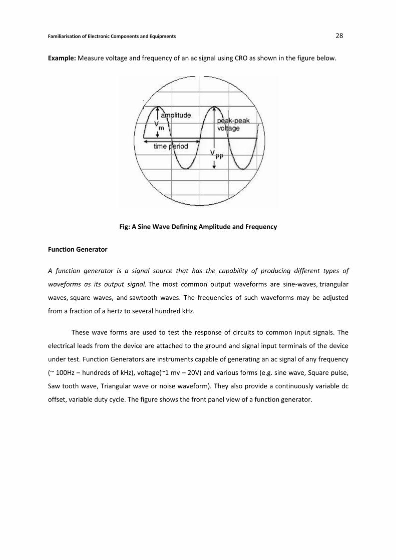
Example: Measure voltage and frequency of an ac signal using CRO as shown in the figure below.
Fig: A Sine Wave Defining Amplitude and Frequency
Function Generator
A function generator is a signal source that has the capability of producing different types of
waveforms as its output signal. The most common output waveforms are sine-waves, triangular
waves, square waves, and sawtooth waves. The frequencies of such waveforms may be adjusted
from a fraction of a hertz to several hundred kHz.
These wave forms are used to test the response of circuits to common input signals. The
electrical leads from the device are attached to the ground and signal input terminals of the device
under test. Function Generators are instruments capable of generating an ac signal of any frequency
(~ 100Hz – hundreds of kHz), voltage(~1 mv – 20V) and various forms (e.g. sine wave, Square pulse,
Saw tooth wave, Triangular wave or noise waveform). They also provide a continuously variable dc
offset, variable duty cycle. The figure shows the front panel view of a function generator.
Page 29
Familiarisation of Electronic Components and Equipments 29
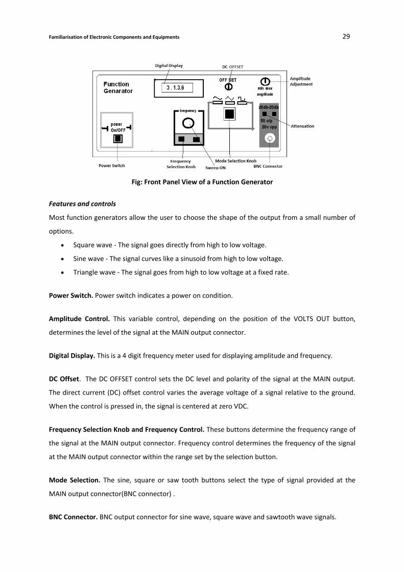
Fig: Front Panel View of a Function Generator
Features and controls
Most function generators allow the user to choose the shape of the output from a small number of
options.
Square wave - The signal goes directly from high to low voltage.
Sine wave - The signal curves like a sinusoid from high to low voltage.
Triangle wave - The signal goes from high to low voltage at a fixed rate.
Power Switch. Power switch indicates a power on condition.
Amplitude Control. This variable control, depending on the position of the VOLTS OUT button,
determines the level of the signal at the MAIN output connector.
Digital Display. This is a 4 digit frequency meter used for displaying amplitude and frequency.
DC Offset. The DC OFFSET control sets the DC level and polarity of the signal at the MAIN output.
The direct current (DC) offset control varies the average voltage of a signal relative to the ground.
When the control is pressed in, the signal is centered at zero VDC.
Frequency Selection Knob and Frequency Control. These buttons determine the frequency range of
the signal at the MAIN output connector. Frequency control determines the frequency of the signal
at the MAIN output connector within the range set by the selection button.
Mode Selection. The sine, square or saw tooth buttons select the type of signal provided at the
MAIN output connector(BNC connector) .
BNC Connector. BNC output connector for sine wave, square wave and sawtooth wave signals.
Page 30
Familiarisation of Electronic Components and Equipments 30
Duty Cycle Control. Activated by the DUTY CYCLE Switch. Rotation from center position adjusts the
duty cycle of the main OUTPUT signal. The duty cycle of a signal refers to the ratio of high voltage to
low voltage time in a square wave signal.
Attenuation Knob(-20 dB,-40 dB). This button is used to obtain the signals in mV range.In -20dB
position the signal at the OUTPUT jack is attenuated by 20dB.In the -40 dB position, the amplitude of
the output signal is attenuated by 40dB(to a few millivolt).Such small signals are used for testing
amplifier circuits.
Using of function generator
After powering on the function generator, the output signal needs to be configured to the
desired shape. Typically, this means connecting the signal and ground leads to an oscilloscope to
check the controls. Adjust the function generator until the output signal is correct, then attach the
signal and ground leads from the function generator to the input and ground of the device under
test. For some applications, the negative lead of the function generator should attach to a negative
input of the device, but usually attaching to ground is sufficient.
Power supply basics
The aim of a DC power supply is to provide the required level of DC power to the load using an AC
supply at the input. Different applications require different attributes, but more often than not these
days DC power supplies provide an accurate output voltage - this is regulated using electronic
circuitry so that it provides a constant output voltage over a wide range of output loads.
In most power supplies there are number of different elements. These may not all be present in
every design.
Input transformer: The input transformer is used to transform the incoming line voltage
down to the required level for the power supply. Typically the input transformer provides a
step down function. It also isolates the output circuit from the line supply.
Rectifier: The power supply rectifier converts the incoming signal from an AC format into
raw DC. Either half wave or more commonly full wave rectifiers may be used as they make
use of both halves of the incoming AC signal.
Smoothing: The raw DC from the rectifier is far from constant falling to zero when the AC
waveform crossed the zero axis, and then rising to its peak. The addition of a reservoir
Page 31
Familiarisation of Electronic Components and Equipments 31
capacitor here fills in the troughs in the waveform, enabling the next stage of the power
supply to operate. Large value capacitors are normally used within this stage.
Regulator: This stage of the power supply takes the smoothed voltage and uses a regulator
circuit to provide a constant output virtually regardless of the output current and any minor
fluctuations in the input level.
Power supply regulation
There are two basic forms of power supply used in electronics equipment:
Unregulated: This form of power supply was the only type used many years ago. It simply
consisted of a rectifier section and this was followed by capacitor or capacitor and inductor
smoothing. There was no regulation to steady the voltage. If a large current was drawn the
voltage would fall as a result of the resistive losses, and also the smoothing would not be as
effective and the level of hum would rise.
Voltage regulated: As transistor circuitry became more commonplace, regulated power
supplies became more common. Today they are almost universally used. They typically
incorporate a voltage reference, and the output voltage is compared to this and altered
accordingly by control circuitry within the regulated power supply.
Multimeter
Multimeter or a multitester is a measurement instrument used in electronics, which is designed
to perform tasks of several measuring instruments. The voltage, current, and resistance
measurements can be made using different options available in a common Multimeter. Therefore, it
is also called VOM (Volt Ohm meter). In more expensive and advanced models, capacitance and
inductance can also be measured and can be used to detect pins of semiconductor elements like
transistors and diodes.
There are two types of multimeters ;analog and digital based on their measurement and display
method.
In Analog Multimeter continuous deflection of a pointer over a scale represents the value of
quantity being measured. Analog meters require no power supply,they give a better visual indication
of changes and suffer less from electrical noise and isolation problems. These meters are simple and
inexpensive.
Page 32
Familiarisation of Electronic Components and Equipments 32
Digital multimeters display a numerical value as the output which has a higher accuracy than
the analog multimeters. Also, advanced digital multimeters offer automatic ranging features so that
the user do not have to select the range of the measurement manually. Additionally, this becomes a
safety feature too. Since no moving parts are inside, the digital multimeters are unaffected by shocks
such as the impact with a solid surface.
Digital multimeter is basically a digital voltmeter and may be used for the measurement of
voltage ,current (D.C or A.C) and resistance.All quantities other than D.C voltage are first converted
into an equivalent D.C voltage by some device. Digital multimeters obtain several samples of the
signal during a short period of time and average the signals to provide better accuracy. The analog
signal is converted into a digital signal by the analog to digital converter, which is the most important
component of the multimeter circuit.
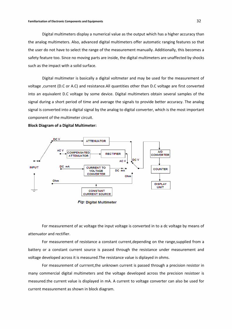
Block Diagram of a Digital Multimeter:
For measurement of ac voltage the input voltage is converted in to a dc voltage by means of
attenuator and rectifier.
For measurement of resistance a constant current,depending on the range,supplied from a
battery or a constant current source is passed through the resistance under measurement and
voltage developed across it is measured.The resistance value is diplayed in ohms.
For measurement of currrent,the unknown current is passed through a precision resistor in
many commercial digital multimeters and the voltage developed across the precision resistoer is
measured.the current value is displayed in mA. A current to voltage converter can also be used for
current measurement as shown in block diagram.
Page 33
Familiarisation of Electronic Components and Equipments 33
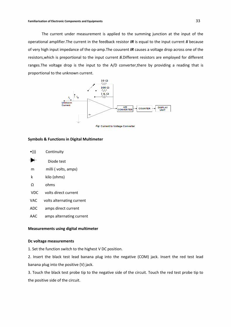
The current under measurement is applied to the summing junction at the input of the
operational amplifier.The current in the feedback resistor IR is equal to the input current Ii because
of very high input impedance of the op-amp.The couurent IR causes a voltage drop across one of the
resistors,which is preportional to the input current Ii.Different resistors are employed for different
ranges.The voltage drop is the input to the A/D converter,there by providing a reading that is
proportional to the unknown current.
Symbols & Functions in Digital Multimeter
•))) Continuity
Diode test
m milli ( volts, amps)
k kilo (ohms)
Ω ohms
VDC volts direct current
VAC volts alternating current
ADC amps direct current
AAC amps alternating current
Measurements using digital multimeter
Dc voltage measurements
1. Set the function switch to the highest V DC position.
2. Insert the black test lead banana plug into the negative (COM) jack. Insert the red test lead
banana plug into the positive (V) jack.
3. Touch the black test probe tip to the negative side of the circuit. Touch the red test probe tip to
the positive side of the circuit.
Page 34
Familiarisation of Electronic Components and Equipments 34
4. Read the voltage in the display. Reset the function switch to successively lower V DC positions to
obtain a higher resolution reading. The display will indicate the proper decimal point and value. If
the polarity is reversed, the display will show (-) minus before the value.
AC Voltage Measurements
1. Set the function switch to the highest V AC position.
2. Insert the black test lead banana plug into the negative (COM) jack. Insert red test lead banana
plug into the positive (V) jack.
3. Touch the black test probe tip to the negative side of the circuit. Touch the red test probe tip to
the positive side of the circuit.
4. Read the voltage in the display. Reset the function switch to successively lower V AC positions to
obtain a higher resolution reading. The display will indicate the proper decimal point and value.
DC Current Measurements
1. Insert the black test lead banana plug into the negative (COM) jack.
2. For current measurements up to 200mA DC, set the function switch to the 200mA DC position and
insert the red test lead banana plug into the (mA) jack.
3. For current measurements up to 10A DC, set the function switch to the 10A range and insert the
red test lead banana plug into the (10A) jack.
4. Remove power from the circuit under test, then open up the circuit at the point where you wish
to measure current.
5. Touch the black test probe tip to the negative side of the circuit. Touch the red test probe tip to
the positive side of the circuit.
6. Apply power to the circuit.
7. Read the current in the display. The display will indicate the proper decimal point and value.
AC Current Measurements
1. Insert the black test lead banana plug into the negative (COM) jack.
2. For current measurements up to 200mA AC, set the function switch to the 200m AAC position and
insert the red test lead banana plug into the (mA) jack.
3. For current measurements up to 10A AC, set the function switch to the 10A range and insert the
red test lead banana plug into the (10A) jack.
4. Remove power from the circuit under test, then open up the circuit at the point where you wish
to measure current.
5. Touch the black test probe tip to the negative side of the circuit. Touch the red test probe tip to
the positive side of the circuit.
Page 35
Familiarisation of Electronic Components and Equipments 35
6. Apply power to the circuit.
7. Read the current in the display. The display will indicate the proper decimal point and value.
RESISTANCE MEASUREMENTS
1. Set the function switch to the highest Ω position.
2. Insert the black test lead banana plug into the negative (COM) jack Insert the red test lead banana
plug into the positive Ω jack.
3. Touch the test probe tips across the circuit or part under test. It is best to disconnect one side of
the
part under test so the rest of the circuit will not interfere with the resistance reading.
4. Read the resistance in the display and then set the function switch to the lowest Ω position that is
greater than the actual or any anticipated resistance. The display will indicate the proper decimal
point and value.
CONTINUITY CHECK
1. Set the function switch to the position.
2. Insert the black lead banana plug into the negative (COM) jack Insert the red test lead banana plug
into the positive (Ω) jack.
3. Touch the test probe tips to the circuit or wire you wish to check.
4. If the resistance is less than approximately 30Ω, the audible signal will sound. If the circuit is open,
the display will indicate “1”.
Diode Test
1. Insert the black test lead banana plug into the negative COM jack and the red test lead banana
plug into the positive diode jack.
2. Turn the function switch to the position.
3. Touch the test probes to the diode under test. Forward voltage will indicate .4 to .5V. Reverse
voltage will indicate “1”. Shorted devices will indicate near 0mV. Shorted devices will indicate near
0mV and an open device will indicate “1” in both polarities. A Zener diode can be verified like a
normal diode as described above. LED diodes usually have a forward voltage drop too high to test
with most multimeters.
Testing Of Bipolar Transistors
The assumption made when testing transistors is that a transistor is just a pair of connected
diodes. Therefore it can be tested for shorts, opens or leakage with a simple analog or digital
Page 36
Familiarisation of Electronic Components and Equipments 36
multimeter. Gain, frequency response, etc. tests can be made only with expensive specialized
instruments.
To test a bipolar transistor with a digital multimeter, take it out of circuit and make the following
measurements using the diode test mode:
Connect the red (positive) lead to the base of the transistor. Connect the black (negative)
lead to the emitter. A good NPN transistor will read a junction drop voltage of 0.4V to 0.9V.
A good PNP transistor will read open.
Leave the red meter lead on the base and move the black meter lead to the collector - the
reading should be almost the same as the previous test, open for PNP and a slightly lower
voltage drop for NPN transistors.
Reverse the meter leads and repeat the test. This time, connect the black meter lead to the
base of the transistor and the red lead to the emitter. A good PNP transistor will read a
junction drop voltage of 0.4V to 0.9V. A good NPN transistor will read open.
Leave the black meter lead on the base and move the red lead to the collector - the reading
should be almost the same as the previous test, open for NPN and a slightly lower voltage
drop for PNP transistors.
Place one meter lead on the collector, the other on the emitter, then reverse. Both tests
should read open for both NPN and PNP transistors.
Identifying the leads and polarity of unknown bipolar transistors
The type (PNP or NPN) and the lead arrangement of unmarked transistors can be
determined easily using a digital, if the transistor is seen as a pair of connected diodes. The
collector and emitter can be identified knowing the fact that the doping for the B-E junction
is always much higher than for the B-C junction, therefore, the forward voltage drop will be
slightly higher. This will show up as a couple of millivolts difference on a digital multimeter's
diode test scale or a slightly higher resistance on an analog VoltOhmMeter.
First make the a few measurements between various leads. Soon you'll identify a lead (the
Base) that will show a forward voltage drop combined with two other leads (the Emitter and
Collector). Now that the Base is identified, observe carefully the voltage drops across B-E
and B-C. The B-C junction will have a slightly less voltage drop.
Page 37
Familiarisation of Electronic Components and Equipments 37
If you arrived at this point, you already know the polarity of the transistor under test. If the
negative lead is placed on the Base when measuring the B-C and B-E voltage drops ,you have a PNP
transistor. Similarly ,if the positive meter lead is placed on the base, you have a NPN transistor.
Transistor hfe Measurement
Set the range switch to the desired hFE position.
Determine the transistor is NPN or PNP type and locate the emitter,base,collector
leads.Insert the leads of the transistor into the proper holes of the hFE socket on the front
panel.
Read the displayed transistor HFE.
Testing Of JFET
JFET can be considered as one PN junction and mearured the resistance between gate and
source or between gate and drain.The meter show low resistance if the positive lead is on gate and
high resistance if the negative lead is on gate.Then it is an N-channel JFET.Since the JFET is a
single,uninterrupted piece of semiconductor material,there is usually no difference between the
source and drian terminals.A reistance check from source to drain should yeild the same value as a
check from drain to source.This resistance should relatively low (a few 100 ohms at most) when the
gate-source PN junction voltage is zero.