Page 1
PRACTICAL WORK BOOK
ELECTRONIC-II (EL-235)
Name :
Roll Number :
Batch :
Department :
Year :
Department of Electronic Engineering
N.E.D. University of Engineering & Technology, Karachi -75270
Pakistan
Hammad Khan
Typewritten Text
For Academic Session 2014
Page 2
LABORATORY WORK BOOK
FOR THE COURSE
EL-235 ELECTRONIC-II
Prepared By: Engr.Saba Ahmed (Lecturer)
Reviewed By: Mr. Ghous Baksh Narejo (Associate Professor)
Approved By:
The Board of Studies of Department of Electronic Engineering
Page 3
Electronic –II (EL-235) Lab Workbook
NED University Of Engineering & Technology- Department of Electronic Engineering
1
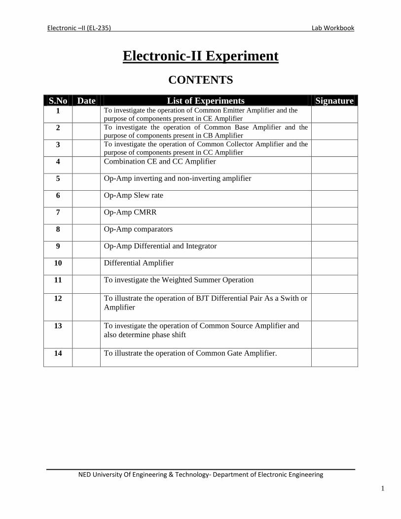
Electronic-II Experiment
CONTENTS
S.No Date List of Experiments Signature 1 To investigate the operation of Common Emitter Amplifier and the
purpose of components present in CE Amplifier 2 To investigate the operation of Common Base Amplifier and the
purpose of components present in CB Amplifier 3 To investigate the operation of Common Collector Amplifier and the
purpose of components present in CC Amplifier 4 Combination CE and CC Amplifier 5 Op-Amp inverting and non-inverting amplifier 6 Op-Amp Slew rate 7 Op-Amp CMRR 8 Op-Amp comparators 9 Op-Amp Differential and Integrator 10 Differential Amplifier 11 To investigate the Weighted Summer Operation
12 To illustrate the operation of BJT Differential Pair As a Swith or
Amplifier
13 To investigate the operation of Common Source Amplifier and
also determine phase shift
14 To illustrate the operation of Common Gate Amplifier.
Page 4
Electronic –II (EL-235) Lab Workbook
NED University Of Engineering & Technology- Department of Electronic Engineering
3
Laboratory No 1
Objective:
To investigate the operation of Common Emitter Amplifier
To describe the purpose of components present in Common Emitter Amplifier
Introduction:
The CE Amplifier is one of the three basic transistor amplifier circuit used in electronic industry. In this
configuration input is applied at the base lead while its output is taken at collector, which is in 180o
phase shift.
Pre-Lab:
1. Students must know about DC parameters i.e. IE ,VE , VB , VC , VCE
2. Must able to draw AC equivalent circuit of CE Amplifier
3. Able to find out Voltage Gain(AV)
4. Purpose of partially by-pass emitter resistance
5. Effect of emitter by-pass capacitor on voltage gain
Apparatus:
Resistors Capacitors Signal generator
150K 10µf Dual trace oscilloscope
2.7K 2.2µf Breadboard
3.9K 2N3904 npn transistor VOM
4.7K 0-15 V dc power supply Breadboard Socket
10K
Schematic Diagram:
Page 5
Electronic –II (EL-235) Lab Workbook
NED University Of Engineering & Technology- Department of Electronic Engineering
4
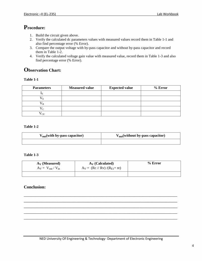
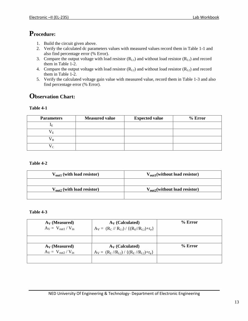
Procedure:
1. Build the circuit given above.
2. Verify the calculated dc parameters values with measured values record them in Table 1-1 and
also find percentage error (% Error).
3. Compare the output voltage with by-pass capacitor and without by-pass capacitor and record
them in Table 1-2.
4. Verify the calculated voltage gain value with measured value, record them in Table 1-3 and also
find percentage error (% Error).
Observation Chart:
Table 1-1
Parameters Measured value Expected value % Error
IE
VE
VB
VC
VCE
Table 1-2
Vout(with by-pass capacitor) Vout(without by-pass capacitor)
Table 1-3
AV (Measured)
AV = Vout / Vin
AV (Calculated)
AV = (Rc // Rv) /(RE1+ re)
% Error
Conclusion:
_____________________________________________________________________________________________
_____________________________________________________________________________________________
_____________________________________________________________________________________________
_____________________________________________________________________________________________
_____________________________________________________________________________________________
Page 6
Electronic –II (EL-235) Lab Workbook
NED University Of Engineering & Technology- Department of Electronic Engineering
5
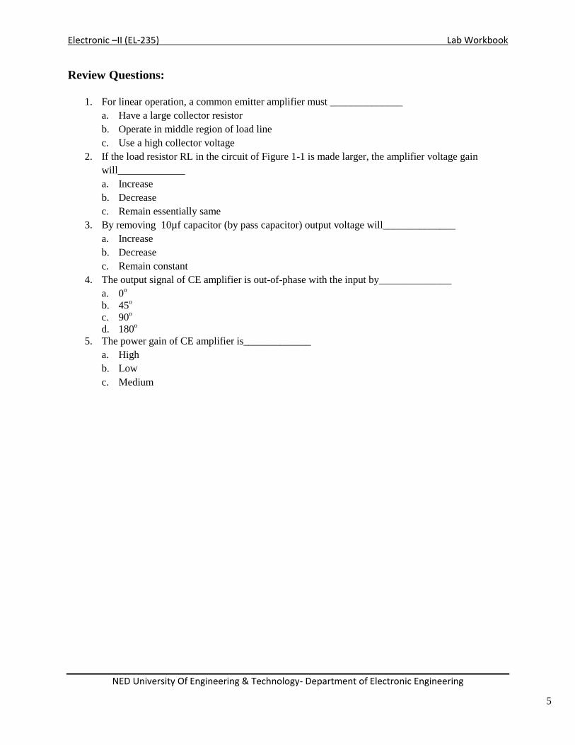
Review Questions:
1. For linear operation, a common emitter amplifier must ______________
a. Have a large collector resistor
b. Operate in middle region of load line
c. Use a high collector voltage
2. If the load resistor RL in the circuit of Figure 1-1 is made larger, the amplifier voltage gain
will_____________
a. Increase
b. Decrease
c. Remain essentially same
3. By removing 10µf capacitor (by pass capacitor) output voltage will______________
a. Increase
b. Decrease
c. Remain constant
4. The output signal of CE amplifier is out-of-phase with the input by______________
a. 0o
b. 45o
c. 90o
d. 180o
5. The power gain of CE amplifier is_____________
a. High
b. Low
c. Medium
Page 7
Electronic –II (EL-235) Lab Workbook
NED University Of Engineering & Technology- Department of Electronic Engineering
6
Experiment No 2
Objective:
To investigate the operation of Common Base Amplifier
To describe the purpose of components present in Common Base Amplifier
Introduction:
In Common base amplifier input is provided at emitter lead while output is taken at Collector, so in
common base both input and output signal are in phase. Voltage gain of common base is like that of
common emitter.
Pre-Lab:
1. Students must know about DC parameters i.e. IE ,VE , VB , VC
2. Students must know about AC parameters i.e. re , AV
3. Must able to draw AC equivalent and DC equivalent circuit of CB Amplifier
4. Able to find out Voltage Gain(AV)
5. Purpose of capacitors used in CB Amplifier
6. Effect of load resistance on voltage gain
Apparatus:
Resistors Capacitors Signal generator
470 10µf Dual trace oscilloscope
1K 100µf Breadboard
10K 2N3904 npn transistor VOM
0-15 V dc power supply
Schematic Diagram:
Page 8
Electronic –II (EL-235) Lab Workbook
NED University Of Engineering & Technology- Department of Electronic Engineering
7
Procedure:
1. Build the circuit given above.
2. Verify the calculated dc parameters values with measured values record them in Table 1-1 and
also find percentage error (% Error).
3. Compare the output voltage with load resistor (RL) and without load resistor (RL) and record them
in Table 1-2.
4. Verify the calculated voltage gain value with measured value, record them in Table 1-3 and also
find percentage error (% Error).
Observation Chart:
Table 1-1
Parameters Measured value Expected value % Error
IE
VE
VB
VC
Table 1-2
Vout(with load resistor) Vout(without load resistor)
Table 1-3
AV (Measured)
AV = Vout / Vin
AV (Calculated)
AV = (Rc // RL) / re
% Error
Conclusion:
_____________________________________________________________________________________________
_____________________________________________________________________________________________
_____________________________________________________________________________________________
_____________________________________________________________________________________________
_____________________________________________________________________________________________
Page 9
Electronic –II (EL-235) Lab Workbook
NED University Of Engineering & Technology- Department of Electronic Engineering
8
Review Questions:
1. The current gain in CB Amplifier is ______________.
a. Less than unity
b. More than unity
c. Unity
2. Which of the following is not the characteristic of CB Amplifier
1. Low input impedance
2. Output taken from collector
3. 180o
phase shift
3. By removing load resistor output voltage will______________.
a. Increase
b. Decrease
c. Remain constant
4. The output signal of CB amplifier is ______________-of-phase with the input.
a. in
b. out
c. In-out
5. The power gain of CB amplifier is_____________.
a. High
b. Low
c. Medium
Page 10
Electronic –II (EL-235) Lab Workbook
NED University Of Engineering & Technology- Department of Electronic Engineering
9
Experiment No 3
Objective:
To investigate the operation of Common Collector Amplifier
To describe the purpose of components present in Common Collector Amplifier
Introduction:
The Common Collector amplifier is also known as ‘Emitter Follower’. In CC Amplifier input is taken at
base while output at emitter. In this configuration output follows input. The input impedance of CC
amplifier is much higher than bipolar transistor amplifier.
Pre-Lab:
1. Students must know about DC parameters i.e. IE ,VE , VB , VC
2. Students must know about AC parameters i.e. re , AV
3. Must able to draw AC and DC equivalent circuit of CC Amplifier
4. Able to find out Voltage Gain(AV)
Apparatus:
Resistors Capacitors Signal generator
68K 100µf Dual trace oscilloscope
1K 2.2µf Breadboard
100 2N3904 npn transistor VOM
22K 0-15 V dc power supply
27K
Schematic Diagram:
Page 11
Electronic –II (EL-235) Lab Workbook
NED University Of Engineering & Technology- Department of Electronic Engineering
10
Procedure:
1. Build the circuit given above.
2. Verify the calculated dc parameters values with measured values record them in Table 1-1 and
also find percentage error (% Error).
3. Compare the output voltage with load resistor (RL) and without load resistor (RL) and record them
in Table 1-2.
4. Verify the calculated voltage gain value with measured value, record them in Table 1-3 and also
find percentage error (% Error).
Observation Chart:
Table 3-1
Parameters Measured value Expected value % Error
IE
VE
VB
VC
Table 3-2
Vout(with load resistor) Vout(without load resistor)
Table 3-3
AV (Measured)
AV = Vout / Vin
AV (Calculated)
AV = (RE // RL) / (RE // RL)+re
% Error
Conclusion:
_____________________________________________________________________________________________
_____________________________________________________________________________________________
_____________________________________________________________________________________________
_____________________________________________________________________________________________
_____________________________________________________________________________________________
Page 12
Electronic –II (EL-235) Lab Workbook
NED University Of Engineering & Technology- Department of Electronic Engineering
11
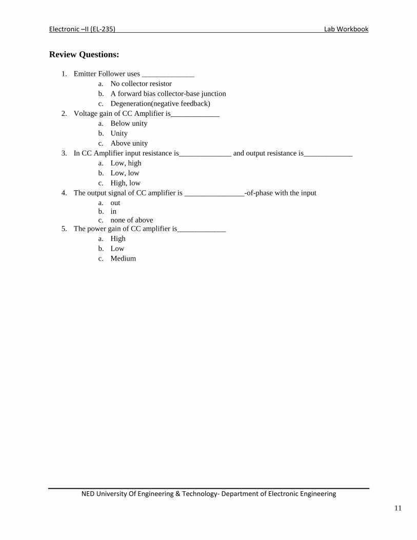
Review Questions:
1. Emitter Follower uses ______________
a. No collector resistor
b. A forward bias collector-base junction
c. Degeneration(negative feedback)
2. Voltage gain of CC Amplifier is_____________
a. Below unity
b. Unity
c. Above unity
3. In CC Amplifier input resistance is______________ and output resistance is_____________
a. Low, high
b. Low, low
c. High, low
4. The output signal of CC amplifier is ________________-of-phase with the input
a. out
b. in
c. none of above
5. The power gain of CC amplifier is_____________
a. High
b. Low
c. Medium
Page 13
Electronic –II (EL-235) Lab Workbook
NED University Of Engineering & Technology- Department of Electronic Engineering
12
Experiment No 4
Objective:
To demonstrate the operation of Combination of CE Amplifier and Emitter Follower (CC) Amplifier
Introduction:
Combination of CE and CC Amplifier is known as phase-splitter or paraphase amplifier which is capable
of producing two identical output signals to identical loads except that they are 180o
out-of-phase with
each other. The output signal from the collector is simply a CE amplifier having unity voltage gain and
also 180o
out-of-phase with the input signal. Output is from the emitter-follower and is in-phase with the
input signal.
Pre-Lab:
1. Students must know about DC and AC parameters of CE and CC Amplifier 2. Purpose of partially by-pass emitter resistance
3. Effect of emitter by-pass capacitor on voltage gain
Apparatus:
Resistors Capacitors Signal generator
1K 2.2µf Dual trace oscilloscope
10K 100 µf Breadboard Socket
2N3904 npn transistor VOM
0-15 V dc power supply
Schematic Diagram:
Page 14
Electronic –II (EL-235) Lab Workbook
NED University Of Engineering & Technology- Department of Electronic Engineering
13
Procedure:
1. Build the circuit given above.
2. Verify the calculated dc parameters values with measured values record them in Table 1-1 and
also find percentage error (% Error).
3. Compare the output voltage with load resistor (RL1) and without load resistor (RL1) and record
them in Table 1-2.
4. Compare the output voltage with load resistor (RL2) and without load resistor (RL2) and record
them in Table 1-2.
5. Verify the calculated voltage gain value with measured value, record them in Table 1-3 and also
find percentage error (% Error).
Observation Chart:
Table 4-1
Parameters Measured value Expected value % Error
IE
VE
VB
VC
Table 4-2
Vout1 (with load resistor) Vout1(without load resistor)
Vout2 (with load resistor) Vout2(without load resistor)
Table 4-3
AV (Measured)
AV = Vout1 / Vin
AV (Calculated)
AV = (RC // RL1) / (RE//RL2)+re
% Error
AV (Measured)
AV = Vout2 / Vin
AV (Calculated)
AV = (RE //RL2) / (RE //RL2)+re
% Error
Page 15
Electronic –II (EL-235) Lab Workbook
NED University Of Engineering & Technology- Department of Electronic Engineering
14
Conclusion:
_____________________________________________________________________________________________
_____________________________________________________________________________________________
_____________________________________________________________________________________________
_____________________________________________________________________________________________
_____________________________________________________________________________________________
Review Questions:
1. The voltage gain at either output for the phase-splitter circuit of Figure 4-1 is______________
a. Increase significantly
b. Decrease significantly
c. Remains essentially the same
2. If RL1 in the circuit is omitted, output voltage will be_____________
a. Increase significantly
b. decrease significantly
c. remains same
3. If RL1 in the circuit is omitted, output voltage will be_____________
a. Increase significantly
b. decrease significantly
c. remains same
4. The two output signals are ________________out-of-phase with each other by
a. 0o
b. 45o
c. 90o
d. 180o
Page 16
Electronic –II (EL-235) Lab Workbook
NED University Of Engineering & Technology- Department of Electronic Engineering
15
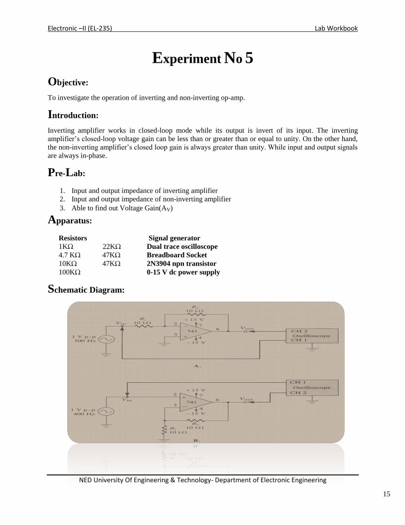
Experiment No 5
Objective:
To investigate the operation of inverting and non-inverting op-amp.
Introduction:
Inverting amplifier works in closed-loop mode while its output is invert of its input. The inverting
amplifier’s closed-loop voltage gain can be less than or greater than or equal to unity. On the other hand,
the non-inverting amplifier’s closed loop gain is always greater than unity. While input and output signals
are always in-phase.
Pre-Lab:
1. Input and output impedance of inverting amplifier
2. Input and output impedance of non-inverting amplifier
3. Able to find out Voltage Gain(AV)
Apparatus:
Resistors Signal generator
1K 22K Dual trace oscilloscope
4.7 K 47K Breadboard Socket
10K 47K 2N3904 npn transistor
100K 0-15 V dc power supply
Schematic Diagram:
Page 17
Electronic –II (EL-235) Lab Workbook
NED University Of Engineering & Technology- Department of Electronic Engineering
16
Procedure:
Inverting Amplifier:
1. Build the circuit given above for inverting amplifier.
2. Adjust the input to 1Vp-p and frequency at 500 Hz. Compare input and output with the help of
oscilloscope.
3. Measure the output Vp-p and record it in Table 5-1.
4. Now by changing the resistor Rf record output Vp-p and gain and record it in Table 5-1.
Non-inverting Amplifier:
1. Build the circuit given above for inverting amplifier.
2. Adjust the input to 1Vp-p and frequency at 500 Hz. Compare input and output with the help of
oscilloscope.
3. Measure the output Vp-p and record it in Table 5-2.
4. Now by changing the resistor Rf record output Vp-p and gain and record it in Table 5-2.
Observation Chart:
Table 5-1: Inverting Amplifier
Rf Measured value(Vout) Measured Gain Expected Gain % Error
10K
22K
47K
100K
4.7K
1K
Table 5-2: Non-inverting Amplifier
Rf Measured value(Vout) Measured Gain Expected Gain % Error
10K
22K
47K
100K
4.7K
1K
Page 18
Electronic –II (EL-235) Lab Workbook
NED University Of Engineering & Technology- Department of Electronic Engineering
17
Conclusion:
_____________________________________________________________________________________________
_____________________________________________________________________________________________
_____________________________________________________________________________________________
_____________________________________________________________________________________________
_____________________________________________________________________________________________
Review Questions:
1. The voltage gain of an inverting amplifier is out-of-phase with its input signal by_____________
a. 0o
b. 45o
c. 90o
d. 180o
2. The voltage gain of an inverting amplifier is out-of-phase with its input signal by_____________
a. 0o
b. 45o
c. 90o
d. 180o
3. The Voltage gain of inverting amplifier is_____________
a. Low, high
b. Low, low
c. High, low
4. The two output signals are ________________out-of-phase with each other by
a. 0o
b. 45o
c. 90o
d. 180o
Page 19
Electronic –II (EL-235) Lab Workbook
NED University Of Engineering & Technology- Department of Electronic Engineering
18
Experiment No 6
Objective:
To investigate the operation of Common Mode Rejection (CMR) of an op-amp.
Introduction:
By the application of same input signal to both inputs of Op-Amp simultaneously is called Common
Mode Rejection (CMR). In this condition, the output voltage of op-amp should be ‘zero’, since op-amp
are not ideal devices therefore at this instant a small but a finite output voltage will present. The Common
Mode input voltage to the generated output voltage is termed as common mode rejection or CMR. CMR
is expressed in decibels. The higher the CMR, the better the rejection and the smaller the output voltage.
CMR (noise) are the result of pick-up of radiated energy on the input lines from adjacent lines.
Pre-Lab:
1. Students must know about inverting and non-inverting configurations
2. Able to find out Voltage Gain (AV)
3. Student also know about Op-amp’s input modes
Apparatus:
Resistors LM741 op-amp (8-pin mini-DIP) VOM
100K Dual trace oscilloscope z 100-K r
10K Breadboard Socket Signal generator
100 Two 0-15 V dc power supply
Schematic Diagram:
Page 20
Electronic –II (EL-235) Lab Workbook
NED University Of Engineering & Technology- Department of Electronic Engineering
19
Procedure:
1. Build the circuit given above.
2. Set oscilloscope as following:
Channel 1: 2 V/division, ac coupling. Channel 2: 0.02 V/division, ac coupling
Time base: 5 ms/division
3. Set the signal to 10V peak-to-peak and a frequency of 60 Hz, measure rms common mode input
and output voltages with the help of VOM and record in Table 6-1.
4. The CMR can be improved by trimming one or more resistor present in Figure given above.
Replace R4 with a 100-KΩ potentiometer and a 10-KΩ resistor, set all connections.
5. Adjust the 100-KΩ potentiometer for minimum output voltage, then observe the output by using
oscilloscope.
6. Repeat step 3 and record the values in Table 6-2.
Observation Chart:
Table 6-1
Parameters Value
Measured common-mode input voltage, Vin(cm) V
Measured common-mode output voltage, Vout(cm) V
Calculated common-mode voltage gain, Acm = Vout(cm) / Vin(cm)
Calculated differential voltage gain, Av(d) = R2/ R1
Calculated common-mode rejection , CMR (dB) = 20 log (Av(d) / Acm ) dB
Table 6-2
Parameters Value
Measured common-mode input voltage, Vin(cm) V
Measured common-mode output voltage, Vout(cm) V
Calculated common-mode voltage gain, Acm = Vout(cm) / Vin(cm)
Calculated differential voltage gain, Av(d) = R2/ R1
Calculated common-mode rejection , CMR (dB) = 20 log (Av(d) / Acm ) dB
Conclusion:
_____________________________________________________________________________________________
_____________________________________________________________________________________________
_____________________________________________________________________________________________
_____________________________________________________________________________________________
_____________________________________________________________________________________________
Page 21
Electronic –II (EL-235) Lab Workbook
NED University Of Engineering & Technology- Department of Electronic Engineering
20
Review Questions:
1. In differential amplifier, the signal applied simultaneously to both input is the ______________
a. Non- inverting input
b. Inverting input
c. Common mode input
2. Differential amplifier CMR is measured in _____________
a. V
b. dB
c. V/ mS
3. An increase in common mode rejection ratio means increase in voltage By removing 10µf
capacitor (by pass capacitor) output voltage will______________
1. Increase
2. Decrease
3. Remain constant
4. The output signal of CE amplifier is out-of-phase with the input by______________
a. 0o
b. 45o
c. 90o
d. 180o
5. The power gain of CE amplifier is_____________
a. High
b. Low
c. Medium
Page 22
Electronic –II (EL-235) Lab Workbook
NED University Of Engineering & Technology- Department of Electronic Engineering
21
Experiment No 7
Objective:
To measure the Slew rate of Op-amp.
Introduction:
Slew rate of an op-amp is defined as the maximum time rate of change of the output voltage of an op-amp
in response to a step input voltage. It is expressed in volts per microsecond; the slew rate depends upon
the frequency response of the internal stages of the op-amp. So higher the slew rate, higher will be the
frequency response. The measurement of the op-amp‘s slew rate is always accomplished with a large
amplifier having unity gain with a high input frequency signal.
Pre-Lab:
1. Student must know basic definition of Slew rate
2. Large signal parameter
Apparatus:
Resistors 741 op-amp (8-pins mini DIP) Signal generator
10K Dual trace oscilloscope 0-15 V dc power supply
Breadboard
Schematic Diagram:
Page 23
Electronic –II (EL-235) Lab Workbook
NED University Of Engineering & Technology- Department of Electronic Engineering
22
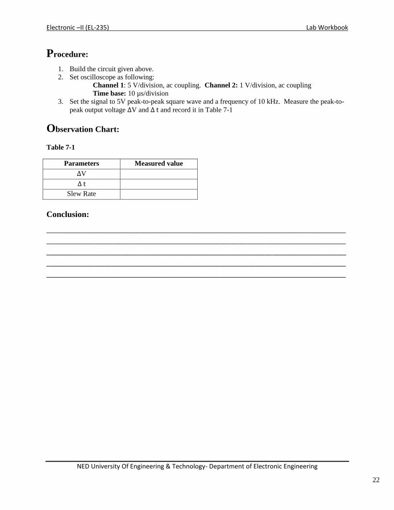
Procedure:
1. Build the circuit given above.
2. Set oscilloscope as following:
Channel 1: 5 V/division, ac coupling. Channel 2: 1 V/division, ac coupling
Time base: 10 µs/division
3. Set the signal to 5V peak-to-peak square wave and a frequency of 10 kHz. Measure the peak-to-
peak output voltage V and and record it in Table 7-1
Observation Chart:
Table 7-1
Parameters Measured value
V
Slew Rate
Conclusion:
_____________________________________________________________________________________________
_____________________________________________________________________________________________
_____________________________________________________________________________________________
_____________________________________________________________________________________________
_____________________________________________________________________________________________
Page 24
Electronic –II (EL-235) Lab Workbook
NED University Of Engineering & Technology- Department of Electronic Engineering
23
Review Questions:
1. The maximum time rate of change of the output voltage of the circuit in response to a step input
is termed as ______________.
a. Gain band-width product
b. Slew rate
c. Output voltage swing
d. Common mode rejection(CMRR)
2. The Slew Rate is usually specified in units of
a. V/s
b. V/ µs
c. 180o
phase shift
3. By using 15V supply, the maximum possible output voltage swing is approximately
a. 5V
b. 15V
c. 20V
d. 30V
4. For an op-amp, the slew rate limits the
a. Input impedance
b. Common-mode rejection
c. Voltage gain
d. Frequency response
5. For the circuit of Fig. 7-1, if the output voltage swings from +5V to -10V in 0.5µs, the slew rate
is
a. 5 V/µs
b. 15 V/µs
c. 20 V/µs
d. 30 V/µs
Page 25
Electronic –II (EL-235) Lab Workbook
NED University Of Engineering & Technology- Department of Electronic Engineering
24
Experiment No 8
Objective:
To verify the operation of inverting and non-inverting comparator using op-amp LM741
Introduction:
A comparator determines whether an input voltage is greater than a predetermined reference level. Since a
comparator operates in an open loop mode, the output voltage approaches either its positive or its
negative supply voltage
Pre-Lab:
1. Comparator using op-amp
2. Inverting and non-inverting Op-amp comparator configuration
Apparatus:
Res istors 741 op-amp (8-pins mini DIP) Signal generator
Two 1 kΩ 0-15 V dc power supply
4.7KΩ Dual trace oscilloscope
Two 10 kΩ Breadboard
47 KΩ
Schematic Diagram:
Page 26
Electronic –II (EL-235) Lab Workbook
NED University Of Engineering & Technology- Department of Electronic Engineering
25
Procedure:
1. Build the circuit given in Fig. 8-1and Fig 8-2.
2. Set oscilloscope as following:
Channel 1: 1 V/division, dc coupling. Channel 2: 10 V/division, dc coupling
Time base: 1ms/division
3. Set the signal to 5V peak-to-peak square wave and a frequency of 300Hz connect oscilloscope at
pin 6 and observe the output waveform.
4. Now build the circuit given in Fig. 8-3.
5. By power on the circuit, LED might glow or not depending potentiometer configuration.
6. If LED is on turn the potentiometer past the point at which LED is off.
7. At this point, measure voltage of op-amp at pin 2 with the help of oscilloscope and record it in
Table 8-1.
Observation Chart:
Table 8-1
R1 Measured VREF Measured VIN(ON)
10 KΩ
47 KΩ
Conclusion:
_____________________________________________________________________________________________
_____________________________________________________________________________________________
_____________________________________________________________________________________________
_____________________________________________________________________________________________
_____________________________________________________________________________________________
Page 27
Electronic –II (EL-235) Lab Workbook
NED University Of Engineering & Technology- Department of Electronic Engineering
26
Review Questions:
1. The reference voltage for the comparator in Fig.8-1
a. 0V
b. +15V
c. -15V
d. None of above
2. The circuit of Fig.8-2 is
a. An inverting comparator
b. A non-inverting comparator
3. For the circuit of Fig. 8-2-2,if the input signal is a sine wave ,The out put signal look like a
a. Sine wave
b. Sine wave, but inverted with respect to the input
c. Square wave
d. Square wave, but inverted with respect to the input
4. For the circuit of Fig. 8-3, If R1 and R2 are 10k Ω, the LED is lit, when the input voltage is
a. Less then -7.5V
b. 0V
c. Greater than 7.5V
d. Any voltage between-7.5V and +7.5V
5. For the circuit of Fig. 8-2,if the input voltage is greater than the reference voltage , the output
voltage is approximately
a. -13V
b. -3V
c. +3V
d. +13V
Page 28
Electronic –II (EL-235) Lab Workbook
NED University Of Engineering & Technology- Department of Electronic Engineering
27
Experiment No 9
Objective:
To verify the operation of differentiator using op-amp
Introduction:
A differentiator is a circuit that calculates the instantaneous slope of the line at every point on waveform.
Differentiator and integrator has opposite operation, by integrating a waveform if waveform is
differentiated original wave from will be obtained.
Pre-Lab:
1. Basic definition of Differentiator
2. Purpose of differentiator
Apparatus:
Res istors 741 op-amp (8-pins mini DIP) Capacitor
2.2 kΩ 0-15 V dc power supply 0.0022µF
10KΩ Dual trace oscilloscope 0.0047 µF
22 kΩ Breadboard
100 KΩ Signal generator
Schematic Diagram:
Page 29
Electronic –II (EL-235) Lab Workbook
NED University Of Engineering & Technology- Department of Electronic Engineering
28
Procedure:
1. Build the circuit given in Fig. 9-1and Fig 9-2.
2. Set oscilloscope as following:
Channel 1: 0.5V/division, dc coupling. Channel 2: 0.05 V/division, dc coupling
Time base: 0.5 ms/division
3. Set the signal to 1V peak-to-peak triangular wave and a frequency of 400Hz connect oscilloscope
at pin 6 and observe the output waveform.
4. Now temporarily remove the probe connected to channel 2 of the oscilloscope and adjust
resulting straight line (ground level), reconnect the output differentiator and measure the negative
peak voltage and record in Table 9-1.
5. Also change the frequency and perform the same steps and record them in Table 9-1.
6. Now by changing oscilloscope setting ;
Channel 1: 0.5V/division, dc coupling. Channel 2: 0.05 V/division, dc coupling
Time base: 0.5 ms/division
7. Observe the difference and record this observation in Table 9-2.
Observation Chart:
Table 9-1
Input frequency Measured Peak output Expected Peak output % Error
400 Hz
1 KHz
30 KHz
Table 9-1
Input frequency Measured Peak output Expected Peak output % Error
400 Hz
1 KHz
30 KHz
Conclusion:
_____________________________________________________________________________________________
_____________________________________________________________________________________________
_____________________________________________________________________________________________
_____________________________________________________________________________________________
_____________________________________________________________________________________________
Page 30
Electronic –II (EL-235) Lab Workbook
NED University Of Engineering & Technology- Department of Electronic Engineering
29
Review Questions:
6. The reference voltage for the comparator in Fig.8-1
d. 0V
e. +15V
f. -15V
g. None of above
7. The circuit of Fig.8-2 is
d. An inverting comparator
e. A non-inverting comparator
8. For the circuit of Fig. 8-2-2,if the input signal is a sine wave ,The out put signal look like a
d. Sine wave
e. Sine wave, but inverted with respect to the input
f. Square wave
g. Square wave, but inverted with respect to the input
9. For the circuit of Fig. 8-3, If R1 and R2 are 10k Ω, the LED is lit, when the input voltage is
e. Less then -7.5V
f. 0V
g. Greater than 7.5V
h. Any voltage between-7.5V and +7.5V
10. For the circuit of Fig. 8-2,if the input voltage is greater than the reference voltage , the output
voltage is approximately
d. -13V
e. -3V
f. +3V
g. +13V
Page 31
Electronic –II (EL-235) Lab Workbook
NED University Of Engineering & Technology- Department of Electronic Engineering
30
Experiment No 10
Objective:
To verify the operation of integrator using op-amp
Introduction:
An integrator is a circuit that computes the area underneath the curve of a given waveform. Differentiator
and integrator are paired mathematical operations in that one has the opposite effect of the other.
Pre-Lab:
1. Basic definition of Integrator
2. Purpose of Integrator
Apparatus:
Res istors 741 op-amp (8-pins mini DIP) Capacitor
2.2 kΩ 0-15 V dc power supply 0.0022µF
10KΩ Dual trace oscilloscope 0.0047 µF
22 kΩ Breadboard
100 KΩ Signal generator
Schematic Diagram:
Page 32
Electronic –II (EL-235) Lab Workbook
NED University Of Engineering & Technology- Department of Electronic Engineering
31
Procedure:
1. Build the circuit given in Fig. 10-1.
2. Set oscilloscope as following:
Channel 1: 0.5V/division, dc coupling. Channel 2: 0.5 V/division, dc coupling
Time base: 20 µs/division
3. Set the signal to 1V peak-to-peak triangular wave and a frequency of 10 KHz connect
oscilloscope at pin 6 and observe the output waveform.
4. Now temporarily remove the probe connected to channel 2 of the oscilloscope and adjust
resulting straight line (ground level), reconnect the output integrator and measure the negative
peak voltage and record in Table 10-1.
5. Also change the frequency and perform the same steps and record them in Table 10-1.
6. Now by changing oscilloscope setting ;
Channel 1: 0.5V/division, dc coupling. Channel 2: 0.5 V/division, dc coupling
Time base: 2 ms/division
7. Observe the difference and record this observation in Table 10-2.
Observation Chart:
Table 10-1
Input frequency Measured Peak output Expected Peak output % Error
400 Hz
1 KHz
30 KHz
Table 10-1
Input frequency Measured Peak output Expected Peak output % Error
400 Hz
1 KHz
30 KHz
Conclusion:
_____________________________________________________________________________________________
_____________________________________________________________________________________________
_____________________________________________________________________________________________
_____________________________________________________________________________________________
_____________________________________________________________________________________________
Page 33
Electronic –II (EL-235) Lab Workbook
NED University Of Engineering & Technology- Department of Electronic Engineering
32
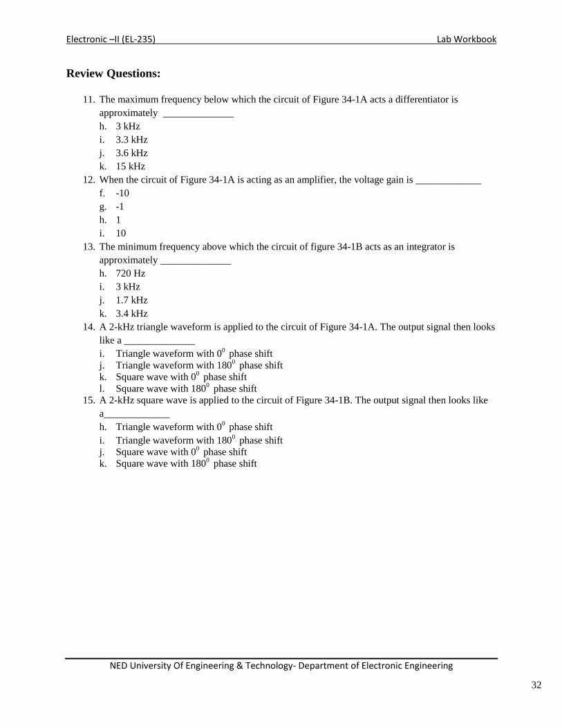
Review Questions:
11. The maximum frequency below which the circuit of Figure 34-1A acts a differentiator is
approximately ______________
h. 3 kHz
i. 3.3 kHz
j. 3.6 kHz
k. 15 kHz
12. When the circuit of Figure 34-1A is acting as an amplifier, the voltage gain is _____________
f. -10
g. -1
h. 1
i. 10
13. The minimum frequency above which the circuit of figure 34-1B acts as an integrator is
approximately ______________
h. 720 Hz
i. 3 kHz
j. 1.7 kHz
k. 3.4 kHz
14. A 2-kHz triangle waveform is applied to the circuit of Figure 34-1A. The output signal then looks
like a ______________
i. Triangle waveform with 00 phase shift
j. Triangle waveform with 1800 phase shift
k. Square wave with 00 phase shift
l. Square wave with 1800 phase shift
15. A 2-kHz square wave is applied to the circuit of Figure 34-1B. The output signal then looks like
a_____________
h. Triangle waveform with 00 phase shift
i. Triangle waveform with 1800 phase shift
j. Square wave with 00 phase shift
k. Square wave with 1800 phase shift
Page 34
Electronic –II (EL-235) Lab Workbook
NED University Of Engineering & Technology- Department of Electronic Engineering
33
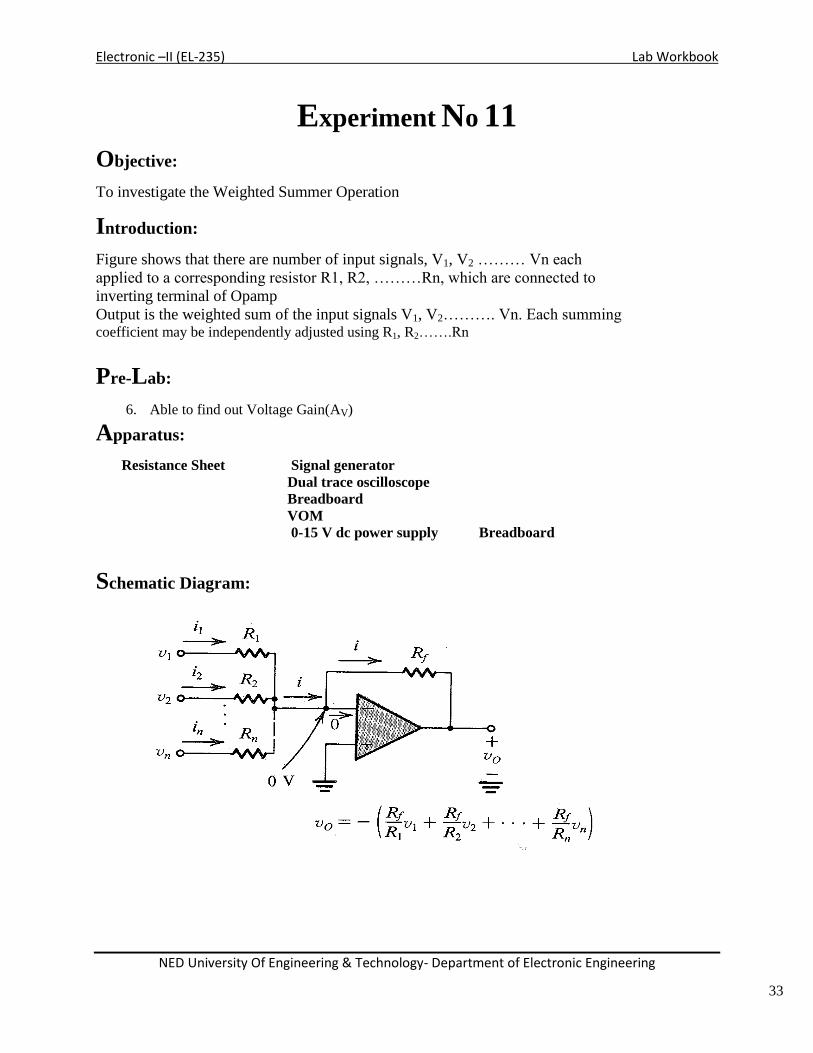
Experiment No 11
Objective:
To investigate the Weighted Summer Operation
Introduction:
Figure shows that there are number of input signals, V1, V2 ……… Vn each
applied to a corresponding resistor R1, R2, ………Rn, which are connected to
inverting terminal of Opamp
Output is the weighted sum of the input signals V1, V2………. Vn. Each summing coefficient may be independently adjusted using R1, R2…….Rn
Pre-Lab:
6. Able to find out Voltage Gain(AV)
Apparatus:
Resistance Sheet Signal generator
Dual trace oscilloscope
Breadboard
VOM
0-15 V dc power supply Breadboard
Schematic Diagram:
Page 35
Electronic –II (EL-235) Lab Workbook
NED University Of Engineering & Technology- Department of Electronic Engineering
34
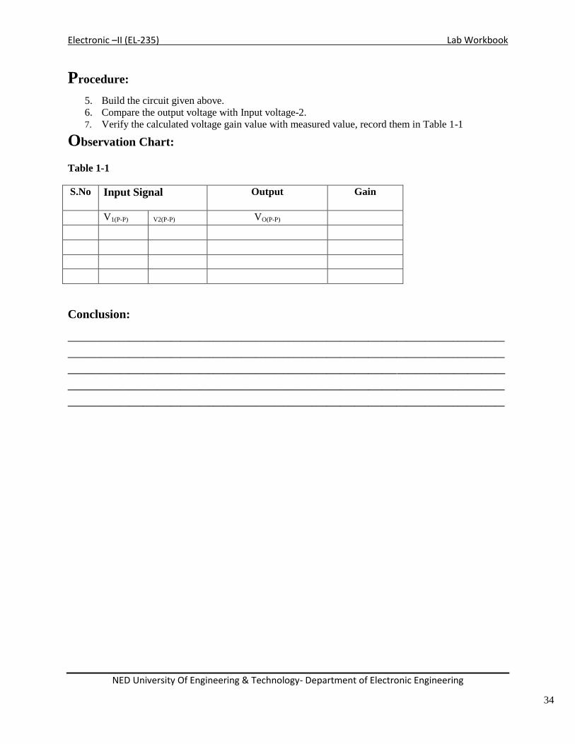
Procedure:
5. Build the circuit given above.
6. Compare the output voltage with Input voltage-2.
7. Verify the calculated voltage gain value with measured value, record them in Table 1-1
Observation Chart:
Table 1-1
S.No Input Signal
Output Gain
V1(P-P) V2(P-P) VO(P-P)
Conclusion:
_____________________________________________________________________________________________
_____________________________________________________________________________________________
_____________________________________________________________________________________________
_____________________________________________________________________________________________
_____________________________________________________________________________________________
Page 36
Electronic –II (EL-235) Lab Workbook
NED University Of Engineering & Technology- Department of Electronic Engineering
35
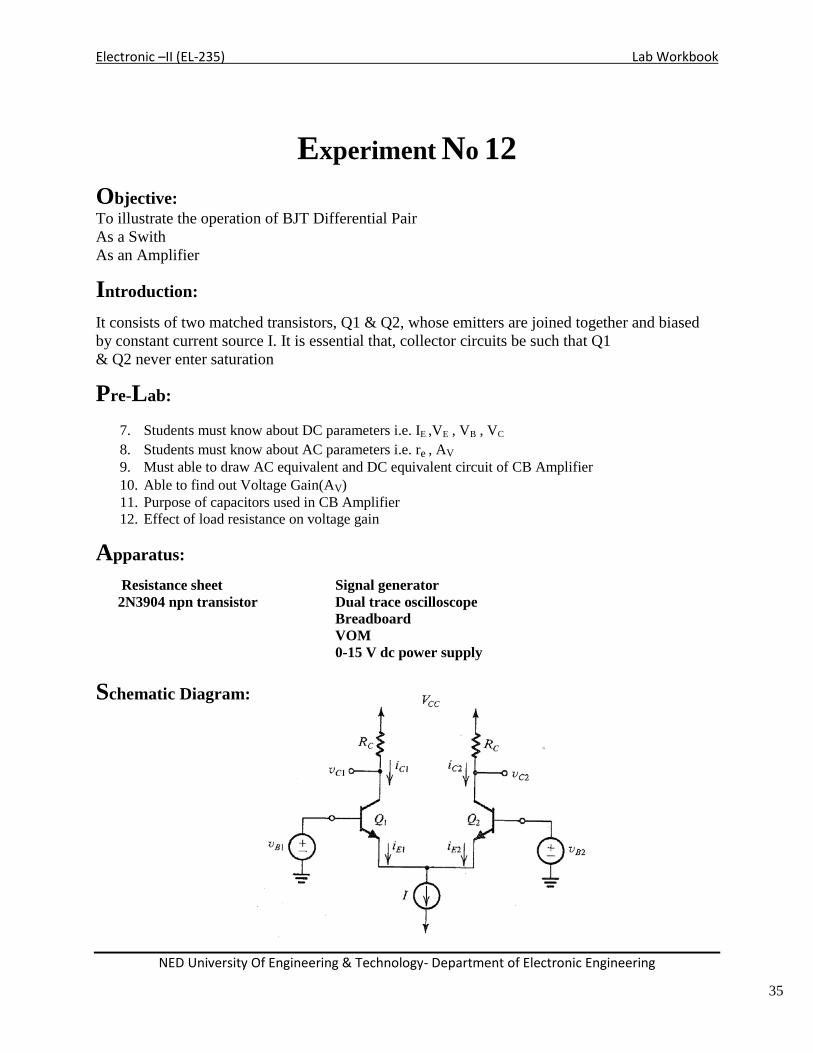
Experiment No 12
Objective:
To illustrate the operation of BJT Differential Pair
As a Swith
As an Amplifier
Introduction:
It consists of two matched transistors, Q1 & Q2, whose emitters are joined together and biased
by constant current source I. It is essential that, collector circuits be such that Q1
& Q2 never enter saturation
Pre-Lab:
7. Students must know about DC parameters i.e. IE ,VE , VB , VC
8. Students must know about AC parameters i.e. re , AV
9. Must able to draw AC equivalent and DC equivalent circuit of CB Amplifier
10. Able to find out Voltage Gain(AV)
11. Purpose of capacitors used in CB Amplifier
12. Effect of load resistance on voltage gain
Apparatus:
Resistance sheet Signal generator
2N3904 npn transistor Dual trace oscilloscope
Breadboard
VOM
0-15 V dc power supply
Schematic Diagram:
Page 37
Electronic –II (EL-235) Lab Workbook
NED University Of Engineering & Technology- Department of Electronic Engineering
36
Procedure:
5. Build the circuit given above.
6. Verify the calculated dc parameters values with measured values record them in Table 1-1
Observation Chart: Table 1-1
S.NO VB1 VB2 VC1 VC2 VC1-VC2
Conclusion:
_____________________________________________________________________________________________
_____________________________________________________________________________________________
_____________________________________________________________________________________________
_____________________________________________________________________________________________
_____________________________________________________________________________________________
Page 38
Electronic –II (EL-235) Lab Workbook
NED University Of Engineering & Technology- Department of Electronic Engineering
37
Experiment No 13
Objective:
To investigate the operation of Common Source Amplifier and also determine phase shift
Introduction:
A Common Source Amplifier or Grounded Source Configuration is shown in figure. To
establish a signal ground, or ac ground, a large capacitor is connected between source &
ground. The signal current bypasses the output resistance of the current source & is called a
bypass Capacitor. Cc1 is known as Coupling Capacitor, & acts as a perfect short circuit
at all signal frequencies of interest
Pre-Lab:
5. Students must know about DC parameters
6. Students must know about AC parameters, AV
7. Able to find out Voltage Gain(AV)
Apparatus:
Resistance Sheet Signal generator
Capacitor: 10µf,0.001nf, 0.1nf Dual trace oscilloscope
Breadboard
VOM
0-15 V dc power supply
Schematic Diagram:
Page 39
Electronic –II (EL-235) Lab Workbook
NED University Of Engineering & Technology- Department of Electronic Engineering
38
Procedure:
5. Build the circuit given above.
6. Verify the calculated dc parameters values with measured values record them in Table 1-1
Observation Chart: Table 1-1
S.NO Frequency Input(p-p) Output(p-p) gain
Conclusion:
_____________________________________________________________________________________________
_____________________________________________________________________________________________
_____________________________________________________________________________________________
_____________________________________________________________________________________________
_____________________________________________________________________________________________
Page 40
Electronic –II (EL-235) Lab Workbook
NED University Of Engineering & Technology- Department of Electronic Engineering
39
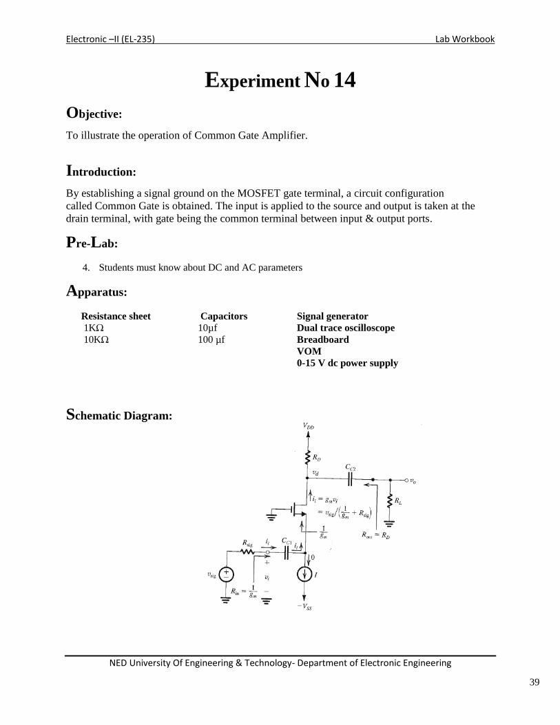
Experiment No 14
Objective:
To illustrate the operation of Common Gate Amplifier.
Introduction:
By establishing a signal ground on the MOSFET gate terminal, a circuit configuration
called Common Gate is obtained. The input is applied to the source and output is taken at the
drain terminal, with gate being the common terminal between input & output ports.
Pre-Lab:
4. Students must know about DC and AC parameters
Apparatus:
Resistance sheet Capacitors Signal generator
1K 10µf Dual trace oscilloscope
10K 100 µf Breadboard
VOM
0-15 V dc power supply
Schematic Diagram:
Page 41
Electronic –II (EL-235) Lab Workbook
NED University Of Engineering & Technology- Department of Electronic Engineering
40
Procedure:
6. Build the circuit given above.
7. Verify the calculated dc parameters values with measured values record them in Table 1-1
Observation Chart:
Table 1-1
S.No Frequency Input(p-p) Output(p-p) gain
1
2
3
4
5
6
7
8
9
10
11
12
Conclusion:
_____________________________________________________________________________________________
_____________________________________________________________________________________________
_____________________________________________________________________________________________
_____________________________________________________________________________________________
_____________________________________________________________________________________________