Page 1
Electronic Structure and Transport in
Graphene/Haeckelite Hybrids: An Ab Initio Study
Zhen Zhu, Zacharias G. Fthenakis and David Tomanek
Physics and Astronomy Department, Michigan State University, East Lansing,
Michigan 48824, USA
E-mail: [email protected]
PACS numbers: 73.40.-c, 61.48.Gh, 73.22.Pr, 73.22.-f
Abstract. We combine ab initio density functional theory (DFT) structural studies
with DFT-based nonequilibrium Green function calculations to investigate how the
presence of non-hexagonal rings affects electronic transport in graphitic structures.
We find that infinite monolayers, finite-width nanoribbons and nanotubes formed of
5-8 haeckelite with only 5- and 8-membered rings are generally more conductive than
their graphene-based counterparts. Presence of haeckelite defect lines in the perfect
graphitic structure, a model of grain boundaries in CVD-grown graphene, increases
the electronic conductivity and renders it highly anisotropic.
Keywords: graphene, haeckelite, hybrid structure, charge transport, DFT
arX
iv:1
502.
0705
0v1
[co
nd-m
at.m
es-h
all]
25
Feb
2015
Page 2
Electronic Structure and Transport in Graphene/Haeckelite Hybrids: An Ab Initio Study2
1. Introduction
Graphene is a unique 2D material that combines extraordinarily high electrical and
thermal conductivity [1, 2] with mechanical strength, flexibility, thermal and chemical
stability. Interest in this system increased significantly after a successful mechanical
exfoliation using a Scotch tape has been reported [3] that yielded large, defect-free
samples. As a scalable alternative to the “Scotch tape” exfoliation technique, chemical
vapor deposition (CVD) is commonly being used now to form graphene monolayers on
metal substrates including Cu [4, 5, 6, 7]. The quality of CVD-grown films is inferior to
those produced by exfoliation, since gas phase deposition leads to simultaneous growth of
graphene flakes that eventually interconnect, forming grain boundaries with a defective,
haeckelite-like structure [8, 9, 10, 11, 12, 13] consisting of non-hexagonal carbon rings
[14]. Pure haeckelite structures and their hybrids with graphene have a significantly
lower thermal conductivity than pure graphene [15]. Only few theoretical studies have
investigated electronic transport in selected graphitic carbon nanostructures with non-
hexagonal rings including hybrid graphene-haeckelite structures [16, 17] and haeckelite
nanotubes [18, 19, 20]
Here we combine ab initio density functional theory (DFT) structural studies
with DFT-based nonequilibrium Green function calculations to investigate how the
presence of non-hexagonal rings affects electronic transport in graphitic structures. We
find that infinite monolayers, finite-width nanoribbons and nanotubes formed of 5-8
haeckelite with only 5- and 8-membered rings are generally more conductive than their
graphene-based counterparts. Presence of haeckelite defect lines in the perfect graphitic
structure, a model of grain boundaries in CVD-grown graphene, increases the electronic
conductivity and renders it highly anisotropic.
Haeckelites [8, 9, 10, 11, 12, 13] consist of periodic 2D arrangements of non-
hexagonal rings of sp2 bonded carbon atoms. Even though these structures have
not been synthesized yet on a large scale, similar atomic arrangements have been
observed (i) in 5-7 and 5-8 defect lines forming the in-plane interface between
adjacent graphene flakes [14, 21, 22], (ii) in a vitreous atomic network formed during
electron-beam irradiation of graphene [23], and (iii) in 5-7 ring structures filling
graphene nanoholes during the healing process of these defects [24]. Most theoretical
studies have focused on the equilibrium structure, stability and growth stability of
haeckelites [8, 9, 10, 11, 12, 13, 17, 25, 26, 27, 28, 29] and found these systems to
be either metallic, semi-metallic or semiconducting [12, 13, 27].
With continuing interest in CVD-grown graphene as an electronic material,
increased attention must be given to carrier scattering at haeckelite-like grain boundaries
connecting defect-free graphene regions. The most plausible model geometry to
investigate charge transport in polycrystalline graphene is that of interconnected strips
of haeckelite and graphene. A consistent picture should be obtained by comparing
the effect of different structural arrangements and widths of haeckelite and graphene
strips on the conductance and its anisotropy. As a counterpart to transport studies in
Page 3
Electronic Structure and Transport in Graphene/Haeckelite Hybrids: An Ab Initio Study3
graphene nanoribbons and nanotubes, we present corresponding results for haeckelite
nanoribbons and nanotubes.
2. Methods
To gain insight into the equilibrium structure, stability and electronic properties of
haeckelite structures, we performed DFT calculations as implemented in the SIESTA
code [30]. Infinite 2D layers and 1D ribbons and nanotubes were separated by 10 A
thick vacuum regions in a 3D periodic arrangement. We used the Ceperley-Alder [31]
exchange-correlation functional as parameterized by Perdew and Zunger [32], norm-
conserving Troullier-Martins pseudopotentials [33], and a double-ζ basis including
polarization orbitals. The reciprocal space was sampled by a fine grid [34] of at least
8×8×1 k-points in the Brillouin zone of the 2D primitive unit cell and its equivalent
for 1D structures or larger 2D supercells. We used a mesh cutoff energy of 180 Ry
to determine the self-consistent charge density, which provided us with a precision in
total energy of .2 meV/atom. All geometries have been optimized using the conjugate
gradient method [35], until none of the residual Hellmann-Feynman forces exceeded
10−2 eV/A.
Electronic transport properties were investigated using the nonequilibrium Green’s
function (NEGF) approach as implemented in the TRAN-SIESTA code [36]. Ballistic
transport calculations for optimized structures were performed using a single-ζ basis
with polarization orbitals, a 180 Ry mesh cutoff energy, and the same k-point grid [34]
as used for structure optimization.
3. Results and discussion
3.1. 5-8 haeckelite
A perfect 2D monolayer of 5-8 haeckelite containing only 5- and 8-membered rings is
shown in Fig. 1(a). The optimum rectangular unit cell is spanned by the Bravais lattice
vectors a1=4.87 A in the x-direction and a2=6.93 A in the y-direction. The 5-8 haeckelite
structure is about 0.36 eV/atom less stable than graphene, which is comparable to the
stability of narrow carbon nanotubes. Due to this relatively high stability, we expect
5-8 haeckelite structures to coexists with graphene at grain boundaries.
The electronic band structure of 5-8 haeckelite is presented in Fig. 1(b). In contrast
to semimetallic graphene, 5-8 haeckelite is metallic and has a finite electronic density of
states at the Fermi level. Whereas the Fermi surface of graphene consists of 6 isolated
k-points, that of 5-8 haeckelite is a line of finite length that intersects the Γ-Y high-
symmetry line, as seen in Fig. 1(b).
The results of our quantum transport calculation for this system are shown in
Fig. 1(c). Besides the improved conductivity over graphene, suggested by the increased
density of states at the Fermi level, we find the conductivity to be also anisotropic, as
expected when considering the atomic arrangement in Fig. 1(a). We find the electrical
Page 4
Electronic Structure and Transport in Graphene/Haeckelite Hybrids: An Ab Initio Study4
Energy (eV)
G/G
0
1
0 -4 -3 -2 -1 0 1 2 3 4
x
graphene y
(a) (b) (c) Pure 5-8 haeckelite
x
y
Fig 1
2
1
EF
-1
-2
En
erg
y (
eV
)
Y Γ M X Γ
Figure 1. (Color online) (a) Atomic structure and (b) electronic band structure of 5-8
haeckelite with only 5- and 8-membered rings. The primitive unit cell is indicated by
the shaded region. (c) Electronic conductance G/G0 along the horizontal x-direction,
shown by the solid red line, and the vertical y-direction, shown by the dashed green
line. G is normalized by the width of the unit cell normal to the transport direction.
E = 0 corresponds to carrier injection at EF .
conductance along the y direction to be much higher than along the x-direction, and
even observe a very narrow transport gap at EF . These findings are consistent with
a very anisotropic Fermi surface that crosses the Γ-Y, but not the Γ-X high-symmetry
line in Fig. 1(b).
3.2. 5-8 haeckelite nanoribbons and nanotubes
Finite-width graphene nanoribbons and carbon nanotubes have received wide attention,
since – unlike infinite graphene monolayers – some of these structures display sizeable
band gaps. In analogy to these structures, we also studied quantum transport in 1D
haeckelite nanoribbons (h-NRs) and nanotubes(h-NTs). In Fig. 2, we present our results
for h-NRs with different widths W that are passivated by hydrogen at the edge. The
atomic structure of the three narrowest haeckelite nanoribbons are shown in Figs. 2(a-c).
We find the optimum lattice constant L≈4.9 A to be nearly independent of the width
W . We also note that structures in Fig. 2(a) and 2(c) have mirror symmetry, whereas
that in Fig. 2(b) does not.
As seen in panels (d-i) of Fig. 2, we found the electronic structure and conductance
of h-NRs to depend sensitively on the ribbon width. Structures with an odd number
of 8-membered rings in the unit cell, depicted in Figs. 2(a) and 2(c), are narrow-gap
semiconductors, with the fundamental band gap decreasing with increasing width from
Eg = 0.05 eV in Fig. 2(a,d) to Eg = 0.02 eV in Fig. 2(c,f). Structures with an even
number of 8-membered rings in the unit cell are all metallic. One example with two
8-membered rings in the unit cell is shown in Fig. 2(b,e). Quantum conductance G of
Page 5
Electronic Structure and Transport in Graphene/Haeckelite Hybrids: An Ab Initio Study5
(a) (b) (c)
(g) (h) (i)
4
2
-2
-4
EF
Γ X
Ene
rgy(
eV)
4
2
-2
-4
EF
4
2
-2
-4
EF
Γ XDOS DOS DOSΓ X
(d) (e) (f)
LL L
WWW
-4 -3 -2 -1 0 1 2 3 4
G/G
0
Energy (eV)
1
0
1
0-4 -3 -2 -1 0 1 2 3 4
Energy (eV)
G/G
0
-4 -3 -2 -1 0 1 2 3 4Energy (eV)
1
0
G/G
0
Fig 5Figure 2. (Color online) Atomic structure, electronic band structure and transport
properties of haeckelite nanoribbons passivated by hydrogen at the edge. Atomic
structure of haeckelite nanoribbons with various width are shown in (a), (b), (c). The
corresponding electronic band structure and density of states is shown in (d), (e), (f),
and ballistic transport conductance G/G0 in (g), (h), (i). The density of state is given
per atom.
the three h-NRs in units of the conductance quantum G0 is shown in Fig. 2(g-i). Of
most interest is the presence or absence of a transport gap at E = 0, corresponding
to carrier injection at EF . As expected, the semiconducting nanoribbons depicted in
Figs. 2(a) and 2(c), have also a finite transport gap, seen in Figs. 2(g) and 2(i). The
metallic nanoribbon in Fig. 2(b) does not have a transport gap at E = 0 according to
Fig. 2(h).
Similar to graphene-based carbon nanotubes, we can construct 5-8 haeckelite-based
nanotubes, and characterize them by the chiral index (n,m) in analogy to carbon
nanotubes. We present the structure and electronic properties of two representative
5-8 haeckelite nanotubes, h-NT(0,2) and h-NT(2,0), in Fig. 3. Both the side and the
end-on view of these nanotubes in Fig. 3(a,b) indicates that their optimum cross-section
is not as round and their surface not as smooth as that of their graphitic counterparts,
owing to the presence of 5- and 8-membered rings. We found the ultra-narrow h-
NT(0,2) and h-NT(2,0) nanotubes to be stable, but highly strained. The stability of
Page 6
Electronic Structure and Transport in Graphene/Haeckelite Hybrids: An Ab Initio Study6
(f)
-4
-3
-2
-1
EF
1
2
3
4
En
erg
y(e
V)
DOS Γ X
h-NT(0,2) h-NT(2,0)
-4
-3
-2
-1
EF
1
2
3
4
DOS Γ X
0
1
-4 -3 -2 -1 0 1 2 3 4 Energy (eV)
(c) (d)
(a) (b) Side view End-on view Side view End-on view
0
1
-4 -3 -2 -1 0 1 2 3 4
G/G
0
Energy (eV)
(e)
Fig 6
Figure 3. (Color online) Structural and electronic properties of haeckelite nanotubes.
Atomic structure of (a) h-NT(0,2) and (b) h-NT(2,0) nanotubes. The length of the
unit cells is denoted by L and the width by W . The corresponding electronic band
structure and density of states is shown in (c), (d), and ballistic transport conductance
G/G0 in (e), (f). The density of state is given per atom.
the narrower h-NT(2,0) is lower by 0.81 eV/atom and that of the wider h-NT(0,2)
is lower by 0.45 eV/atom with respect to the planar haeckelite structure depicted in
Fig. 1(a).
The electronic band structure and density of states of the h-NT(0,2) nanotube,
shown in Fig. 3(c), indicates that h-NT(0,2) is metallic and has a non-zero density of
states at the Fermi energy. As expected, also the calculated quantum conductance,
shown in Fig. 3(e), indicates non-vanishing quantum conductance at E = 0. Quite
different are the electronic structure and quantum conductance results for the h-
NT(2,0) nanotube, shown in Fig. 3(d) and 3(f), which display a very small fundamental
and transport gap of < 0.1 eV. Unlike in graphene-based carbon nanotubes, there
is no general rule to predict whether a given h-NT nanotube should be metallic or
semiconducting.
Page 7
Electronic Structure and Transport in Graphene/Haeckelite Hybrids: An Ab Initio Study7
6-5-8
structure
h-(1,1) h-(3,1) h-(5,1)
(a) (b) (c)
Density o
f sta
tes
Energy (eV) Energy (eV)
Fig 2
(d) (e) (f)
x
y
W
W
W
L
L
L
Energy (eV) EF EF EF
graphene
h-(1,1)
graphene
h-(3,1)
graphene
h-(5,1)
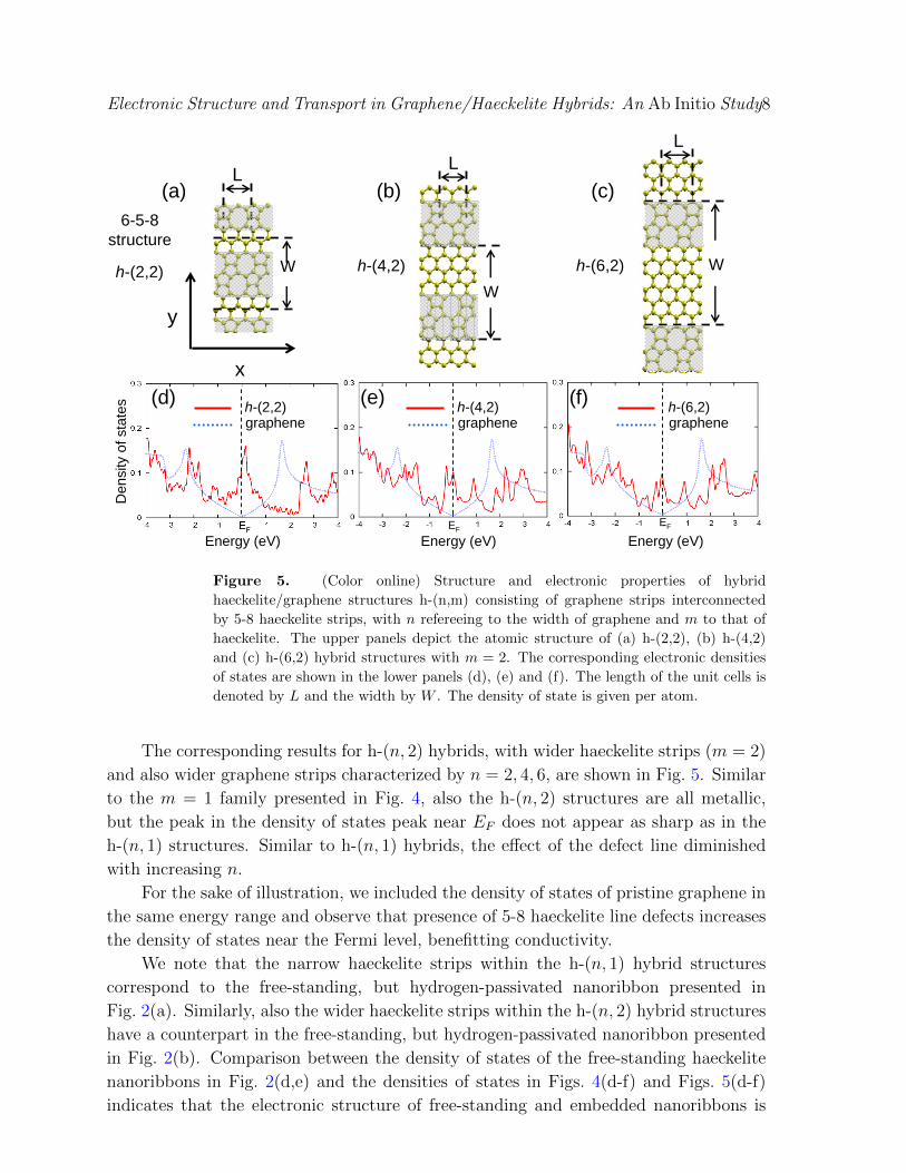
Figure 4. (Color online) Structure and electronic properties of hybrid
haeckelite/graphene structures h-(n,m) consisting of graphene strips interconnected
by 5-8 haeckelite strips, with n refereeing to the width of graphene and m to that of
haeckelite. The upper panels depict the atomic structure of (a) h-(1,1), (b) h-(3,1)
and (c) h-(5,1) hybrid structures with m = 1. The corresponding electronic densities
of states are shown in the lower panels (d), (e) and (f). The length of the unit cells is
denoted by L and the width by W . The density of state is given per atom.
3.3. Hybrid haeckelite-graphene structures
As a model of haeckelite-like grain boundaries connecting graphene grains in
polycrystalline graphene samples, we construct hybrid haeckelite-graphene structures
consisting of strips of 5-8 h-NRs of various width inter-connecting bare zigzag graphene
nanoribbons with different widths. The hybrid systems, identified as h-(n,m), are
characterized by the number m of 8-membered rings per unit cell and the number n of
hexagonal rings across the width of the unit cell. We explored two families of hybrid
structures with m = 1 and m = 2, but different values of n. These studies let us explore
how the density of 5-8 line defects should affect the electronic and transport properties
of the hybrid structures.
The optimum atomic arrangement and electronic structure of h-(n, 1) hybrids, with
n = 1, 3, 5, is shown in Fig. 4. We found all the structures to be metallic, as indicated by
the peak in electronic densities of states at the Fermi energy in Figs. 4(d-f). The peak
is associated with the 5-8 defects and decreases in strength with decreasing fraction of
these defects in the structure, as the graphene strips become wider.
Page 8
Electronic Structure and Transport in Graphene/Haeckelite Hybrids: An Ab Initio Study8
h-(2,2) h-(4,2) h-(6,2)
(a) (b) (c) 6-5-8
structure
Energy (eV) Energy (eV) Energy (eV)
Fig 5
x
y
WW
W
L LL
EF
h-(6,2)graphene
EF
h-(4,2)graphene
Den
sity
of s
tate
s h-(2,2)graphene
(d) (e) (f)
Figure 5. (Color online) Structure and electronic properties of hybrid
haeckelite/graphene structures h-(n,m) consisting of graphene strips interconnected
by 5-8 haeckelite strips, with n refereeing to the width of graphene and m to that of
haeckelite. The upper panels depict the atomic structure of (a) h-(2,2), (b) h-(4,2)
and (c) h-(6,2) hybrid structures with m = 2. The corresponding electronic densities
of states are shown in the lower panels (d), (e) and (f). The length of the unit cells is
denoted by L and the width by W . The density of state is given per atom.
The corresponding results for h-(n, 2) hybrids, with wider haeckelite strips (m = 2)
and also wider graphene strips characterized by n = 2, 4, 6, are shown in Fig. 5. Similar
to the m = 1 family presented in Fig. 4, also the h-(n, 2) structures are all metallic,
but the peak in the density of states peak near EF does not appear as sharp as in the
h-(n, 1) structures. Similar to h-(n, 1) hybrids, the effect of the defect line diminished
with increasing n.
For the sake of illustration, we included the density of states of pristine graphene in
the same energy range and observe that presence of 5-8 haeckelite line defects increases
the density of states near the Fermi level, benefitting conductivity.
We note that the narrow haeckelite strips within the h-(n, 1) hybrid structures
correspond to the free-standing, but hydrogen-passivated nanoribbon presented in
Fig. 2(a). Similarly, also the wider haeckelite strips within the h-(n, 2) hybrid structures
have a counterpart in the free-standing, but hydrogen-passivated nanoribbon presented
in Fig. 2(b). Comparison between the density of states of the free-standing haeckelite
nanoribbons in Fig. 2(d,e) and the densities of states in Figs. 4(d-f) and Figs. 5(d-f)
indicates that the electronic structure of free-standing and embedded nanoribbons is
Page 9
Electronic Structure and Transport in Graphene/Haeckelite Hybrids: An Ab Initio Study9
h-(1,1) h-(3,1) h-(5,1)
Transport: G/G0/W (W is the unit width)
h-(2,2) h-(4,2) h-(6,2)
Co
nd
ucta
nce G
/G0
Energy (eV) Energy (eV) Energy (eV)
(d) (e) (f)
(a) (b) (c)
Fig 4
x y graphene
x y graphene
x y graphene
x y graphene
x y graphene
x y graphene
Co
nd
ucta
nce G
/G0
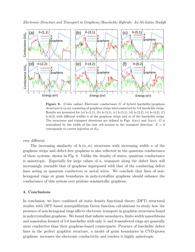
Figure 6. (Color online) Electronic conductance G of hybrid haeckelite/graphene
structures h-(n,m) consisting of graphene strips interconnected by 5-8 haeckelite strips.
Results are presented for (a) h-(1,1), (b) h-(3,1), (c) h-(5,1), (d) h-(2,2), (e) h-(4,2), (f)
h-(6,2) with different widths n of the graphene strips and m of the haeckelite strips.
The structures and transport directions are defined in Figs. 4(a-c) and 5(a-c). G is
normalized by the width of the unit cell normal to the transport direction. E = 0
corresponds to carrier injection at EF .
very different.
The increasing similarity of h-(n,m) structures with increasing width n of the
graphene strips and defect-free graphene is also reflected in the quantum conductance
of these systems, shown in Fig. 6. Unlike the density of states, quantum conductance
is anisotropic. Especially for large values of n, transport along the defect lines will
increasingly resemble that of graphene superposed with that of the conducting defect
lines acting as quantum conductors or metal wires. We conclude that lines of non-
hexagonal rings at grain boundaries in polycrystalline graphene should enhance the
conductance of this system over pristine semimetallic graphene.
4. Conclusions
In conclusion, we have combined ab initio density functional theory (DFT) structural
studies with DFT-based nonequilibrium Green function calculations to study how the
presence of non-hexagonal rings affects electronic transport in graphitic structures found
in polycrystalline graphene. We found that infinite monolayers, finite-width nanoribbons
and nanotubes formed of 5-8 haeckelite with only 5- and 8-membered rings are generally
more conductive than their graphene-based counterparts. Presence of haeckelite defect
lines in the perfect graphitic structure, a model of grain boundaries in CVD-grown
graphene, increases the electronic conductivity and renders it highly anisotropic.
Page 10
Electronic Structure and Transport in Graphene/Haeckelite Hybrids: An Ab Initio Study10
Acknowledgments
The authors acknowledge financial support from the National Science Foundation
Cooperative Agreement No. EEC-0832785, titled “NSEC: Center for High-rate
Nanomanufacturing”. Computational resources have been provided by the Michigan
State University High Performance Computing Center.
References
[1] Novoselov K S, Geim A K, Morozov S V, Jiang D, Zhang Y, Dubonos S V, Grigorieva I V and
Firsov A A 2004 Science 306 666–669 URL http://dx.doi.org/10.1126/science.1102896
[2] Bolotin K, Sikes K, Jiang Z, Klima M, Fudenberg G, Hone J, Kim P and Stormer H 2008 Solid
State Commun. 146 351–355 URL http://www.sciencedirect.com/science/article/pii/
S0038109808001178
[3] Novoselov K S, Jiang D, Schedin F, Booth T J, Khotkevich V V, Morozov S V and Geim A K
2005 Proc. Natl. Acad. Sci. U.S.A 102 10451–10453
[4] Kim K S, Zhao Y, Jang H, Lee S Y, Kim J M, Kim K S, Ahn J H, Kim P, Choi J Y and Hong
B H 2009 Nano Lett. 457 706 URL http://dx.doi.org/10.1038/nature07719
[5] Reina A, Jia X, Ho J, Nezich D, Son H, Bulovic V, Dresselhaus M S and Kong J 2009 Nano Lett.
9 30 URL http://dx.doi.org/10.1021/nl801827v
[6] Kim K S, Zhao Y, Jang H, Lee S Y, Kim J M, Kim K S, Ahn J H, Kim P, Choi J Y and Hong
B H 2009 Nature 457(7230) 706–710 URL http://dx.doi.org/10.1038/nature07719
[7] Li X, Cai W, An J, Kim S, Nah J, Yang D, Piner R, Velamakanni A, Jung I, Tutuc E, Banerjee
S K, Colombo L and Ruoff R S 2009 Science 324 1312–1314 URL http://www.sciencemag.
org/content/324/5932/1312.abstract
[8] Crespi V H, Benedict L X, Cohen M L and Louie S G 1996 Phys. Rev. B 53(20) R13303–R13305
[9] Terrones H, Terrones M, Hernandez E, Grobert N, Charlier J C and Ajayan P M 2000 Phys. Rev.
Lett. 84(8) 1716–1719
[10] Wang X Q, Li H D and Wang J T 2013 Phys. Chem. Chem. Phys. 15(6) 2024–2030
[11] Lusk M T and Carr L D 2008 Phys. Rev. Lett. 100(17) 175503
[12] Appelhans D J, Lin Z and Lusk M T 2010 Phys. Rev. B 82(7) 073410
[13] Appelhans D J, Carr L D and Lusk M T 2010 New J. Phys. 12 125006
[14] Huang P Y, Ruiz-Vargas C S, van der Zande A M, Whitney W S, Levendorf M P, Kevek J W,
Garg S, Alden J S, Hustedt C J, Zhu Y, Park J, McEuen P L and Muller D A 2011 Nature 469
389–392 URL http://dx.doi.org/10.1038/nature09718
[15] Fthenakis Z G, Zhu Z and Tomanek D 2014 Phys. Rev. B 89(12) 125421
[16] Botello-Mendez A R, Cruz-Silva E, Lopez-Urıas F, Sumpter B G, Meunier V, Terrones M and
Terrones H 2009 ACS Nano 3 3606–3612 pMID: 19863086
[17] Rocquefelte X, Rignanese G M, Meunier V, Terrones H, Terrones M and Charlier J C 2004 Nano
Lett. 4 805–810
[18] Lisenkov S, Andriotis A N, Ponomareva I and Menon M 2005 Phys. Rev. B 72(11) 113401
[19] Li Y F, Li B R and Zhang H L 2008 J. Phys. Cond. Matter 20 415207
[20] Popovic Z, Milosevic I and Damnjanovic M 2011 Mat. Sci. Eng. B 176 494–496
[21] Lahiri J, Lin Y, Bozkurt P, Oleynik I I and Batzill M 2010 Nat. Nanotechnol. 5(5) 326–329
[22] Huang P Y, Ruiz-Vargas C S, van der Zande A M, Whitney W S, Levendorf M P, Kevek J W,
Garg S, Alden J S, Hustedt C J, Zhu Y, Park J, McEuen P L and Muller D A 2011 Nature 469
389–392
[23] Eder F R, Kotakoski J, Kaiser U and Meyer J C 2014 Sci. Rep. 4 4060
[24] Zan R, Ramasse Q M, Bangert U and Novoselov K S 2012 Nano Lett. 12 3936–3940
[25] Wang Y, Page A J, Nishimoto Y, Qian H J, Morokuma K and Irle S 2011 J. Am. Chem. Soc. 133
Page 11
Electronic Structure and Transport in Graphene/Haeckelite Hybrids: An Ab Initio Study11
18837–18842 (Preprint http://dx.doi.org/10.1021/ja2064654) URL http://dx.doi.org/
10.1021/ja2064654
[26] Enyashin A N and Ivanovskii A L 2011 phys. stat. sol. (b) 248 1879–1883 ISSN 1521-3951
[27] Su C, Jiang H and Feng J 2013 Phys. Rev. B 87(7) 075453
[28] Sheng X L, Cui H J, Ye F, Yan Q B, Zheng Q R and Su G 2012 J. Appl. Phys. 112 074315
[29] Liu Y, Wang G, Huang Q, Guo L and Chen X 2012 Phys. Rev. Lett. 108 225505
[30] Artacho E, Anglada E, Dieguez O, Gale J D, Garcia A, Junquera J, Martin R M, Ordejon P,
Pruneda J M, Sanchez-Portal D and Soler J M 2008 J. Phys. Cond. Matter 20 064208
[31] Ceperley D M and Alder B J 1980 Phys. Rev. Lett. 45(7) 566–569
[32] Perdew J P and Zunger A 1981 Phys. Rev. B 23(10) 5048–5079
[33] Troullier N and Martins J L 1991 Phys. Rev. B 43 1993
[34] Monkhorst H J and Pack J D 1976 Phys. Rev. B 13(12) 5188–5192
[35] Hestenes M R and Stiefel E 1952 J. Res. Natl. Bur. Stand. 49 409–436
[36] Brandbyge M, Mozos J L, Ordejon P, Taylor J and Stokbro K 2002 Phys. Rev. B 65(16) 165401