PoS(TWEPP-17)109 Electronics and Firmware of the Belle II Silicon Vertex Detector Readout System The Silicon Vertex Detector of the Belle II Experiment at KEK in Tsukuba, Japan, consists of 172 double-sided strip sensors. They are read out by 1748 APV25 chips, and the analog data are sent out of the radiation zone to 48 modules which convert them to digital. FPGAs then compensate line signal distortions using digital finite impulse response filters and detect data frames from the incoming stream. Then they perform pedestal subtraction, common mode correction and zero suppression, as well as calculate the peak timing and amplitude of each event from a set of data samples using a neural network. Topical Workshop on Electronics for Particle Physics 11 - 14 September 2017 Santa Cruz, California R. Thalmeier b (Corresponding author; E-mail: [email protected]), K. Adamczyk r , H. Aihara o , C. Angelini h,i , T. Aziz g , V. Babu g , S. Bacher r , S. Bahinipat d , E. Barberio a , Ti. Baroncelli a , To. Baroncelli a , A. K. Basith e , G. Batgnani h,i , A. Bauer b , P. K. Behera e , T. Bergauer b , S. Bearini h,i , B. Bhuyan f , T. Bilka c , F. Bosi i , L. Bosisio j,k , A. Bozek r , F. Buchsteiner b , L. Bulla b , G. Caria a , G. Casarosa i , M. Ceccant i , D. Cervenkov c , S. R. Chendvankar g , N. Dash d , G. De Pietro h,i , S. T. Divekar g , Z. Doležal c , D. Dua g , F. Fort h,i , M. Friedl b , B. Gobbo k , K. Hara p , T. Higuchi l , T. Horiguchi n , C. Irmler b , A. Ishikawa n , H. B. Jeon q , C. Joo l , J. Kandra c , N. Kambara p , K. H. Kang q , T. Kawasaki C,m , P. Kodyš c , T. Kohriki p , S. Koike E,p , M. M. Kolwalkar g , I. Komarov k , R. Kumar s , W. Kun o , P. Kvasnicka c , C. La Licata j,k , L. Lanceri j,k , S. C. Lee q , J. Leenbichler b , J. Libby e , T. Lueck h,i , M. Maki p , P. Mammini i , A. Martni h,i , S. N. Mayekar g , G. B. Mohanty g , S. Mohanty A,g , T. Morii l , K. R. Nakamura p , Z. Natkaniec r , Y. Onuki o , W. Ostrowicz r , A. Paladino l , E. Paoloni h,i , H. Park q , F. Pilo i , A. Profet i , I. Rashevskaya B,k , K. K. Rao g , G. Rizzo h,i , Resmi P. K. e , M. Rozanska r , J. Sasaki o , N. Sato p , S. Schultschik b , C. Schwanda b , Y. Seino m , N. Shimizu o , J. Stypula r , J. Suzuki p , S. Tanaka p , G. N. Taylor a , R. Thomas g , T. Tsuboyama p , S. Uozumi q , P. Urquijo a , L. Vitale j,k , S. Watanuki n , M. Watanabe D,m , I. J. Watson o , J. Webb a , J. Wiechczynski r , S. Williams a , B. Würkner b , H. Yamamoto n , H. Yin b , T. Yoshinobu m , L. Zani h,i (Belle-II SVD Collaboraton) a School of Physics, University of Melbourne, Melbourne, Victoria 3010, Australia b Institute of High Energy Physics, Austrian Academy of Sciences, 1050 Vienna, Austria c Faculty of Mathematics and Physics, Charles University, 121 16 Prague, Czech Republic d Indian Institute of Technology Bhubaneswar, Satya Nagar, India e Indian Institute of Technology Madras, Chennai 600036, India f Indian Institute of Technology Guwahati, Assam 781039, India g Tata Institute of Fundamental Research, Mumbai 400005, India, A also at Utkal University, Bhubaneswar 751004, India h Dipartimento di Fisica, Università di Pisa, I-56127 Pisa, Italy i INFN Sezione di Pisa, I-56127 Pisa, Italy j Dipartimento di Fisica, Università di Trieste, I-34127 Trieste, Italy k INFN Sezione di Trieste, I-34127 Trieste, Italy, B presently at TIFPA - INFN, I-38123 Trento, Italy l Kavli Institute for the Physics and Mathematics of the Universe (WPI), University of Tokyo, Kashiwa 277-8583, Japan m Department of Physics, Niigata University, Niigata 950-2181, Japan, C presently at Kitasato University, Sagamihara 252-0373, Japan, D presently at Nippon Dental University, Niigata 951-8580, Japan n Department of Physics, Tohoku University, Sendai 980-8578, Japan o Department of Physics, University of Tokyo, Tokyo 113-0033, Japan p High Energy Accelerator Research Organization (KEK), Tsukuba 305-0801, Japan, E deceased q Department of Physics, Kyungpook National University, Daegu 702-701, Korea r H. Niewodniczanski Institute of Nuclear Physics, Krakow 31-342, Poland s Punjab Agricultural University, Ludhiana 141004, India Copyright owned by the author(s) under the terms of the Creative Commons Attribution-NonCommercial-NoDerivatives 4.0 International License (CC BY-NC-ND 4.0).
Transcript
PoS(TWEPP-17)109
Electronics and Firmware of the Belle II Silicon VertexDetector Readout System
The Silicon Vertex Detector of the Belle II Experiment at KEK in Tsukuba, Japan, consists of 172double-sided strip sensors. They are read out by 1748 APV25 chips, and the analog data are sentout of the radiation zone to 48 modules which convert them to digital. FPGAs then compensate linesignal distortions using digital finite impulse response filters and detect data frames from theincoming stream. Then they perform pedestal subtraction, common mode correction and zerosuppression, as well as calculate the peak timing and amplitude of each event from a set of datasamples using a neural network.
Topical Workshop on Electronics for Particle Physics11 - 14 September 2017Santa Cruz, California
R. Thalmeierb (Corresponding author; E-mail: [email protected] ),K. Adamczykr, H. Aiharao, C. Angelinih,i, T. Azizg, V. Babug, S. Bacherr, S. Bahinipatd, E. Barberioa, Ti. Baroncellia, To. Baroncellia, A. K. Basithe, G. Batgnanih,i, A. Bauerb, P. K. Beherae, T. Bergauerb, S. Bettarinih,i, B. Bhuyanf, T. Bilkac, F. Bosii, L. Bosisioj,k, A. Bozekr, F. Buchsteinerb, L. Bullab, G. Cariaa, G. Casarosai, M. Ceccanti, D. Cervenkovc, S. R. Chendvankarg, N. Dashd, G. De Pietroh,i, S. T. Divekarg, Z. Doležalc, D. Duttag, F. Forth,i, M. Friedlb, B. Gobbok, K. Harap, T. Higuchil, T. Horiguchin, C. Irmlerb, A. Ishikawan, H. B. Jeonq, C. Jool, J. Kandrac, N. Kambarap, K. H. Kangq, T. KawasakiC,m, P. Kodyšc, T. Kohrikip, S. KoikeE,p, M. M. Kolwalkarg, I. Komarovk, R. Kumars, W. Kuno, P. Kvasnickac, C. La Licataj,k, L. Lancerij,k, S. C. Leeq, J. Lettenbichlerb, J. Libbye, T. Lueckh,i, M. Makip, P. Mamminii, A. Martnih,i, S. N. Mayekarg, G. B. Mohantyg, S. MohantyA,g, T. Moriil, K. R. Nakamurap, Z. Natkaniecr, Y. Onukio, W. Ostrowiczr, A. Paladinol, E. Paolonih,i, H. Parkq, F. Piloi, A. Profeti, I. RashevskayaB,k, K. K. Raog, G. Rizzoh,i, Resmi P. K.e, M. Rozanskar, J. Sasakio, N. Satop, S. Schultschikb, C. Schwandab, Y. Seinom, N. Shimizuo, J. Stypular, J. Suzukip, S. Tanakap, G. N. Taylora, R. Thomasg, T. Tsuboyamap, S. Uozumiq, P. Urquijoa, L. Vitalej,k, S. Watanukin, M. WatanabeD,m, I. J. Watsono, J. Webba, J. Wiechczynskir, S. Williamsa, B. Würknerb, H. Yamamoton, H. Yinb, T. Yoshinobum, L. Zanih,i
(Belle-II SVD Collaboraton)
a School of Physics, University of Melbourne, Melbourne, Victoria 3010, Australiab Institute of High Energy Physics, Austrian Academy of Sciences, 1050 Vienna, Austriac Faculty of Mathematics and Physics, Charles University, 121 16 Prague, Czech Republicd Indian Institute of Technology Bhubaneswar, Satya Nagar, Indiae Indian Institute of Technology Madras, Chennai 600036, Indiaf Indian Institute of Technology Guwahati, Assam 781039, Indiag Tata Institute of Fundamental Research, Mumbai 400005, India, A also at Utkal University, Bhubaneswar 751004, Indiah Dipartimento di Fisica, Università di Pisa, I-56127 Pisa, Italyi INFN Sezione di Pisa, I-56127 Pisa, Italyj Dipartimento di Fisica, Università di Trieste, I-34127 Trieste, Italyk INFN Sezione di Trieste, I-34127 Trieste, Italy, B presently at TIFPA - INFN, I-38123 Trento, Italyl Kavli Institute for the Physics and Mathematics of the Universe (WPI), University of Tokyo, Kashiwa 277-8583, JapanmDepartment of Physics, Niigata University, Niigata 950-2181, Japan, C presently at Kitasato University, Sagamihara 252-0373, Japan, D presently at Nippon Dental University, Niigata 951-8580, Japan
n Department of Physics, Tohoku University, Sendai 980-8578, Japano Department of Physics, University of Tokyo, Tokyo 113-0033, Japanp High Energy Accelerator Research Organization (KEK), Tsukuba 305-0801, Japan, E deceasedq Department of Physics, Kyungpook National University, Daegu 702-701, Korear H. Niewodniczanski Institute of Nuclear Physics, Krakow 31-342, Polands Punjab Agricultural University, Ludhiana 141004, India
Copyright owned by the author(s) under the terms of the Creative Commons Attribution-NonCommercial-NoDerivatives 4.0 International License (CC BY-NC-ND 4.0).
Electronics and Firmware of the Belle II Silicon Vertex Detector Readout System
1. Introduction
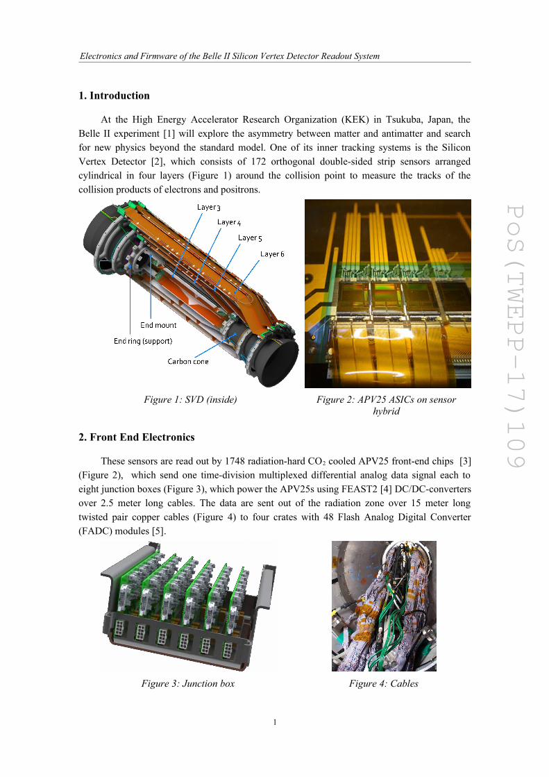
At the High Energy Accelerator Research Organization (KEK) in Tsukuba, Japan, theBelle II experiment [1] will explore the asymmetry between matter and antimatter and searchfor new physics beyond the standard model. One of its inner tracking systems is the SiliconVertex Detector [2], which consists of 172 orthogonal double-sided strip sensors arrangedcylindrical in four layers (Figure 1) around the collision point to measure the tracks of thecollision products of electrons and positrons.
Figure 1: SVD (inside) Figure 2: APV25 ASICs on sensorhybrid
2. Front End Electronics
These sensors are read out by 1748 radiation-hard CO2 cooled APV25 front-end chips [3](Figure 2), which send one time-division multiplexed differential analog data signal each toeight junction boxes (Figure 3), which power the APV25s using FEAST2 [4] DC/DC-convertersover 2.5 meter long cables. The data are sent out of the radiation zone over 15 meter longtwisted pair copper cables (Figure 4) to four crates with 48 Flash Analog Digital Converter(FADC) modules [5].
Figure 3: Junction box Figure 4: Cables
1
PoS(TWEPP-17)109
Electronics and Firmware of the Belle II Silicon Vertex Detector Readout System
3. FADC Modules
These FADC modules (Figure 5) convert the analog data to digital using one flash analogdigital converter per APV25 chip. Each module also includes a field programmable gate array(FPGA) chip, namely a Stratix IV GX.
Figure 5: FADC module
Figure 6: FADC module data processing
2
PoS(TWEPP-17)109
Electronics and Firmware of the Belle II Silicon Vertex Detector Readout System
The data processing part (Figure 6) of the firmware inside this FPGA compensates linesignal distortions using digital finite impulse response (FIR) filters and detects data frames inthe incoming streams. It reorders the data so that it matches the physical arrangement of thedetector, and performs pedestal subtraction to eliminate static offsets, common modesubtraction to remove event-by-event baseline shifts and zero suppression to discard empty stripdata. The peak timing and amplitude of each event is calculated from a set of data samples usinga neural network in real-time.
The processed data are sent to another detector sub-system, namely the pixel detector, toprovide information for timing and the determination of spatial regions of interests, as well as tothe Data Acquisition System [6].
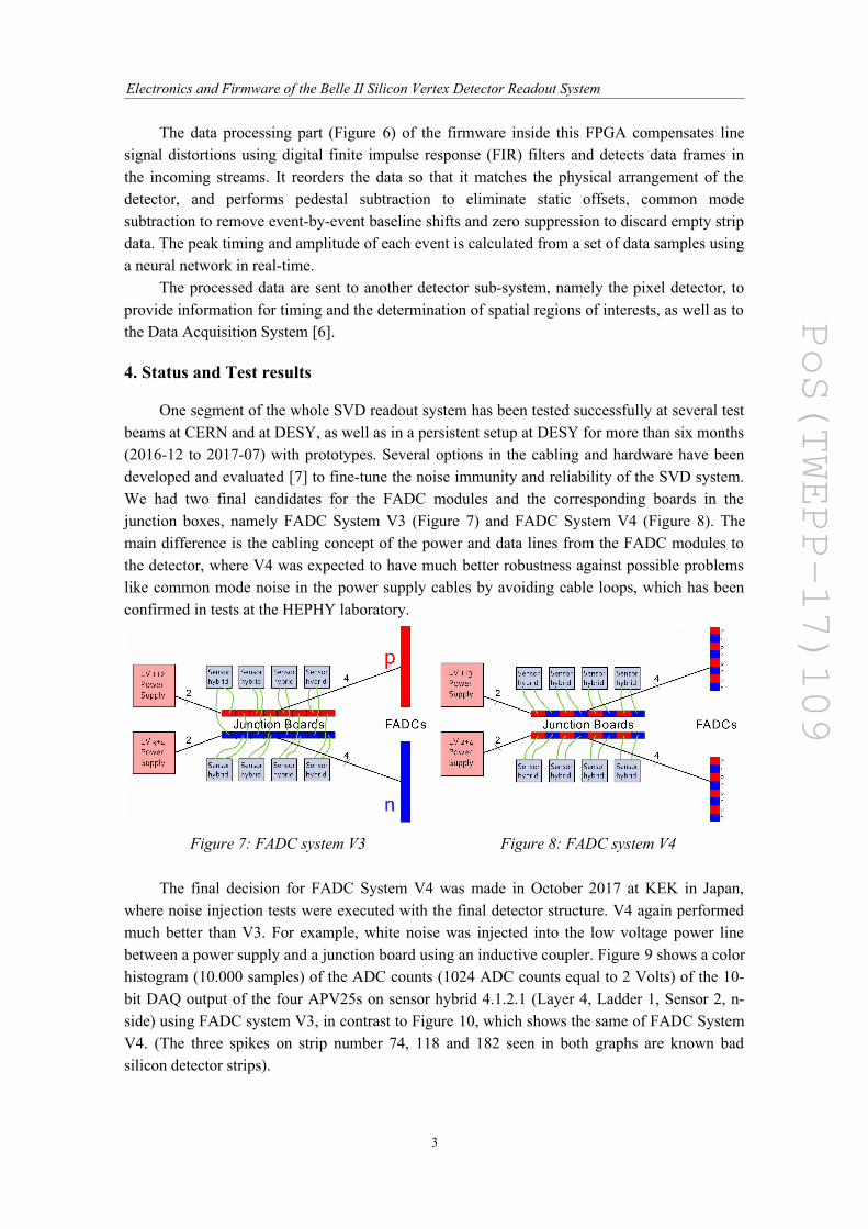
4. Status and Test results
One segment of the whole SVD readout system has been tested successfully at several testbeams at CERN and at DESY, as well as in a persistent setup at DESY for more than six months(2016-12 to 2017-07) with prototypes. Several options in the cabling and hardware have beendeveloped and evaluated [7] to fine-tune the noise immunity and reliability of the SVD system.We had two final candidates for the FADC modules and the corresponding boards in thejunction boxes, namely FADC System V3 (Figure 7) and FADC System V4 (Figure 8). Themain difference is the cabling concept of the power and data lines from the FADC modules tothe detector, where V4 was expected to have much better robustness against possible problemslike common mode noise in the power supply cables by avoiding cable loops, which has beenconfirmed in tests at the HEPHY laboratory.
Figure 7: FADC system V3 Figure 8: FADC system V4
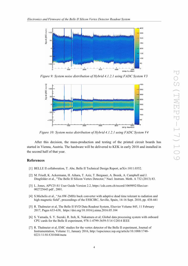
The final decision for FADC System V4 was made in October 2017 at KEK in Japan,where noise injection tests were executed with the final detector structure. V4 again performedmuch better than V3. For example, white noise was injected into the low voltage power linebetween a power supply and a junction board using an inductive coupler. Figure 9 shows a colorhistogram (10.000 samples) of the ADC counts (1024 ADC counts equal to 2 Volts) of the 10-bit DAQ output of the four APV25s on sensor hybrid 4.1.2.1 (Layer 4, Ladder 1, Sensor 2, n-side) using FADC system V3, in contrast to Figure 10, which shows the same of FADC SystemV4. (The three spikes on strip number 74, 118 and 182 seen in both graphs are known badsilicon detector strips).
3
PoS(TWEPP-17)109
Electronics and Firmware of the Belle II Silicon Vertex Detector Readout System
Figure 9: System noise distribution of Hybrid 4.1.2.1 using FADC System V3
Figure 10: System noise distribution of Hybrid 4.1.2.1 using FADC System V4
After this decision, the mass-production and testing of the printed circuit boards hasstarted in Vienna, Austria. The hardware will be delivered to KEK in early 2018 and installed inthe second half of that year.
References
[1] BELLE II collaboration, T. Abe, Belle II Technical Design Report, arXiv:1011.0352.
[2] M. Friedl, K. Ackermann, H. Aihara, T. Aziz, T. Bergauer, A. Bozek, A. Campbell and J. Dingfelder et al., "The Belle II Silicon Vertex Detector," Nucl. Instrum. Meth. A 732 (2013) 83.
[3] L. Jones, APV25-S1 User Guide Version 2.2, https://cds.cern.ch/record/1069892/files/cer-002725643.pdf , 2001.
[4] S.Michelis et al., “An 8W-2MHz buck converter with adaptive dead time tolerant to radiation and high magnetic field”, proceedings of the ESSCIRC, Seville, Spain, 14-16 Sept. 2010, pp. 438-441
[5] R. Thalmeier et al, The Belle II SVD Data Readout System, Elsevier Volume 845, 11 February 2017, Pages 633-638, https://doi.org/10.1016/j.nima.2016.05.104
[7] R. Thalmeier et al, EMC studies for the vertex detector of the Belle II experiment, Journal of Instrumentation, Volume 11, January 2016, http://iopscience.iop.org/article/10.1088/1748-0221/11/01/C01044/meta