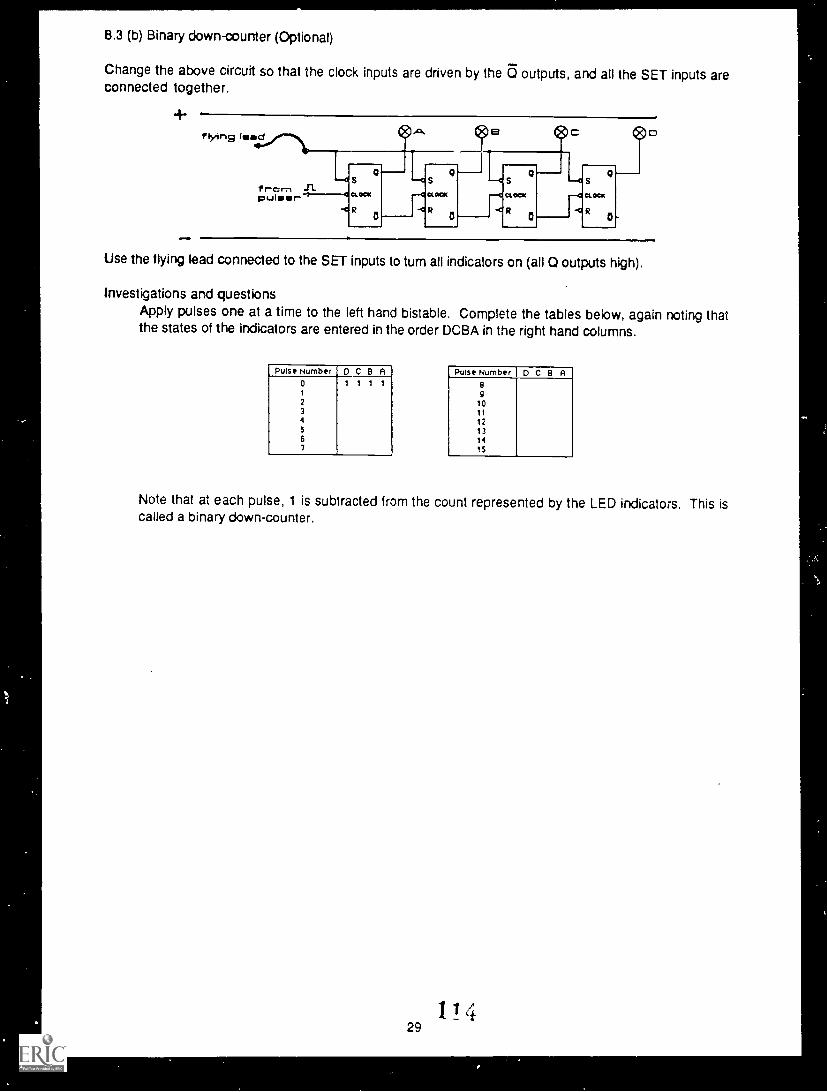
DOCUMENT RESUME ED 357 971 SE 053 263 AUTHOR Lewis, John TITLE Electronics Teacher's Guide. Science and Technology Document Series No. 40. INSTITUTION United Nations Educational, Scientific, and Cultural Organ;zation, Paris (France). Section of Science and Technology Education. REPORT NO ED-91/WS-1 PUB DATE 91 NOTE 119p.; Part of the Science and Technology Education Document Series, No. 40. AVAILABLE FROM Science and Technology Education Section, Educational Development Division, Education Sector, Unesco, 7 Flace de Fontenoy, 75700 Paris, France. PUB TYPE Guides Classroom Use Instructional Materials (For Learner) (051) Guides Classroom Use Teaching Guides (For Teacher) (052) EDRS PRICE MF01/PC05 Plus Postage. DESCRIPTORS Curriculum Guides; *Electric Circuits; Electricity; *Electronics; *Physics; *Science Activities; *Science Curriculum; Science Education; *Science Experiments; Secondary Education; Worksheets IDENTIFIERS *Logic Circuits; UNESCO ABSTRACT This is the second document on the teaching of electronics to appear as part of UNESCO's science and technology education program. An introductory section describes the role that electronics plays as part of the physics curriculum. The following section outlines the content of the electronics course. The outline includes guidelines for determining the course content. The remainder of the document is divided into two parts that present the nine sections of the course. The theme of the three sections in the first part is switching. The theme of the six sections in the second part is integrated circuits. The nine section topics are: (1) useful electronic components; (2) switches; (3) logic circuits; (4) logic gates; (5) bistable circuits; (6) drivers; (7) coding; (3) the pulser, the astable, and the clocked bistable; and (9) counting circuits. Each section contains experiments related to the topic that include investigation questions and notes about the experiment. An attached workbook at the back of the document contains student worksheets for the experiments in each of the sections. Two appendices provide a bibliography and technical details for the electronic modules involved in the experiments. (MDH) *********************************************************************** Reproductions supplied by EDRS are the best that can be made from the original document. ***********************************************************************
Transcript
DOCUMENT RESUME
ED 357 971 SE 053 263
AUTHOR Lewis, JohnTITLE Electronics Teacher's Guide. Science and Technology
Document Series No. 40.INSTITUTION United Nations Educational, Scientific, and Cultural
Organ;zation, Paris (France). Section of Science andTechnology Education.
REPORT NO ED-91/WS-1PUB DATE 91
NOTE 119p.; Part of the Science and Technology EducationDocument Series, No. 40.
AVAILABLE FROM Science and Technology Education Section, EducationalDevelopment Division, Education Sector, Unesco, 7Flace de Fontenoy, 75700 Paris, France.
PUB TYPE Guides Classroom Use Instructional Materials (ForLearner) (051) Guides Classroom Use TeachingGuides (For Teacher) (052)
EDRS PRICE MF01/PC05 Plus Postage.DESCRIPTORS Curriculum Guides; *Electric Circuits; Electricity;
This is the second document on the teaching ofelectronics to appear as part of UNESCO's science and technologyeducation program. An introductory section describes the role thatelectronics plays as part of the physics curriculum. The followingsection outlines the content of the electronics course. The outlineincludes guidelines for determining the course content. The remainderof the document is divided into two parts that present the ninesections of the course. The theme of the three sections in the firstpart is switching. The theme of the six sections in the second partis integrated circuits. The nine section topics are: (1) usefulelectronic components; (2) switches; (3) logic circuits; (4) logicgates; (5) bistable circuits; (6) drivers; (7) coding; (3) thepulser, the astable, and the clocked bistable; and (9) countingcircuits. Each section contains experiments related to the topic thatinclude investigation questions and notes about the experiment. Anattached workbook at the back of the document contains studentworksheets for the experiments in each of the sections. Twoappendices provide a bibliography and technical details for theelectronic modules involved in the experiments. (MDH)
No. 11 Agriculture and Biology Teaching. 1984 (English)No. 12 Health Education and Biology Teaching. 1984 (English)
No. 13 The Training of Primary Science Educators - A WorkshopApproach. 1985 (English)
No. 14 L'Economie sociale familiale dans le developpement rural.1985 (French)
No. 15 Human Development and Evolution and Biology Teachi1985 (English)
No. 16 Assessment: A Practical Guide to Improving the Quality andScope of Assessment Instruments. 1986 (English)
No. 17 Practical Activities for Out-of-School Science and TechnologyEducation. 1986 (English)
No. 18 The Social Relevance of Science and Technology Education.1986 (English)
2
3 4
Cover photos
1. Photo Unesco,Paul Almasy
2. Photo UNATIONS
3 Photo UnescoiD. Bahrman
4. Photo rights reserved
No. 19 The Teaching of Science and Technology in an Interdisciplin-ary Contex. 1986 (English)
No. 20 Mathematics for All. 1986 (English, French in press)
No. 21 Science and Mathematics in the General Secondary Schoolin the Soviet Union. 1986 (English)
No. 22 Leisure, Values & Biology Teaching. 1987 (English and
French)
No. 23 Use of Sea and its Organisms. 1987 (English)No. 24 Innovations in Science and Mathematics Education in the
Soviet Union. 1987 (English)No. 25 Biology and Human Welfare. Case Studies in Teaching
plied Biology. 1988 (English)No. 26 Sourcebook of Science Education Research in the Carib-
bean. 1988 (English)No. 27 Pour un enseignement integre de la science et de la technolo-
gie : trois modules. 1988 (French)No. 28 Microbiological Techniques in School. 1988 (English)
No. 29 Games and Toys in the Teaching of Science and Technology.1988 (English and French)
No. 30 Field Work in Ecology for Secondary Schools in TropicalCountries. 1988 (English, Arabic)
No. 31 Educational Materials Linking Technology Teaching withScience Education: Technology in Life. 1988 (English)
No. 32 Evaluation and Assessment in Mathematics Education. 1989(English)
No. 33 Systems Thinking in Biology Education. 1989 (English)
No. 34 Base physique de l'electronique clans I'enseignement secon-daire : module methodologique. 1989 (French)
No. 35 Mathematics, Education, and Society. 1889 (English)
No. 36 Biblir=.1raphy in Integrated Science Teaching. 1990 (English)
No. 37 EducaciOn Matematica en las Americas VII. 1990 (Spanish)
No. 38 The Teaching of Science and Technology in an Interdiscip-linary Context. 1990 (English)
No. 39 Teaching Biotechnology in Schools. 1990 (English)
ED-91/WS-1
Science and Technology EducationDocument Series No. 40
ElectronicsTeacher's Guide
John Lewis
Section of Scienceand Technology Education
UNESCO Paris, 1991
Preface
This document, the second to appear on the teaching of electronics in the 'Scienceand technology education document series', has been prepared as part of Unesco'sscience and technology education programme. The previous title, Base physiqued'electronique dans l'enseignement secondaire: module methodologique (Science andtechnology education document series, 34) exists in French only.
Electronics Teacher's Guide has been specially written by John Lewis forUnesco. He was one of the leaders of the well known Nuffield 0-Level PhysicsCurriculum project and later the director of the Science & Society Project in theUnited Kingdom. He has contributed worldwide to many innovations in scienceeducation. Mr. Lewis has been Secretary of the International Commission ofPhysics Education, which awarded him its medal in 1988, and Secretary of theCommittee on the Teaching of Science of the International Council of ScientificUnions. His committee organized the Bangalore Conference on 'Science andTechnology Education and Future Human Needs' in 1985. He was awarded theOBE for his work in science education.
This work is based on material developed at the Independent SchoolsMicroelectronics Centre (ISMEC) at Westminster College, a:ford. ISMEC itselfceased to exist when its work was completed in 1986. Its place has been taken bythe Westminster Centre for Design and Technology.
Unesco wishes to express its appreciation first to John Lewis, MichaelSummers and Geoffrey Foxcroft for the original development of the material andthen to John Lewis, Geoffrey Foxcroft and David Haynes for the development ofthis modified version for Unesco. The views expressed in this report are those ofthe author and not necessarily those of Unesco.
Comments on the contents of this document are welcomed; they should besent to:
Science and Technology Education SectionEducational Development DivisionEducation SectorUnesco7 Place de Fontenoy75700 ParisFrance
Base physique d'electronique dans l'enseignement secondaire: module methodologique isavailable free of charge from the same address.
CONT'NTS
Elcatronics as part of the Physics Curriculum page 1
An Outline of Content page 3
The modules for Part 1 page 5
Introduction to Part 1 page 6
Section 1 : Some Usefu! Electronic Components page 7
Section 8 : The Pulser, the Astable and the Clocked Bistable page 53
Section 9 : Counting Circuits page 58
Appendix A : Bibliography page 72
Appendix B : Technical Details page 73
A
,
Electronics as Part of the Physics Curriculum
Whereas most educators are now agreed on the importance of including electronics within the school
curriculum, there are conflicting views on how this should be done. Traditionally, of course, someelectronics has always been part of school physics. In the past it has largely been confined to the higher
levels, but most people would now agree that a much wider exposure is necessary (in fact many would
argue that electronics should be a compulsory part of the curriculum). The problem with the traditionalapproach to electronics within physics is that it has been centred on particular devices and their
characteristics. In earlier days, valves and their uses for rectification and amplification were a focus of
attention, and more recently, transistors (both bipolar and FET) and other solid state devices have been
prominent in physics curricula at advanced levels.
However, any approach which places too much emphasis on the structure and characteristics of specific
devices suffers from two major drawbacks. The first is that these devices are likely to be of only transient
importance (witness valves, or indeed, transistors). Secondly, not enough time will be left over to provide
experience of designing and building electronic systems to perform useful tasks. The latter is vital if
students are to acquire some appreciation and understanding of the power of modern electronics, of its
role in technology, and of its influence on human societies.
Of course, not all physics courses have adopted this traditional device-centred approach. The most
notable exception is the Nuffield Advanced Physics course, which pioneered an approach to electronics
teaching using conceptual building bricks. Electronics is still about logic gates, bistables, astables,counters, and so on, even though we now use integrated circuits instead of valves or transistors. The real
insight of the Nuffield course (which in fact used transistors) was to realise this basic conceptual durability
in the face of rapid technological development at the device level. It is this kind of approach - known as the
systems approach which is now so urgently required at an earlier stage.
Despite the success of the systems approach within the Nuffield course, there are still many physics
teachers who argue that this kind of electronics has little to do with physics, and has no place in a physics
curriculum. Before considering this fundamental question, let us first identify some of the very practical
advantages of keeping electronics (but now a systems approach) within school physics courses.
Of paramount importance is the difficulty of finding time for a new subject electronics - within an already
crowded school curriculum. This problem is resolved if electronics is taught within the existing curriculum
structure (physics, of course, is part of that structure).
One has only to look at the requirements of electronics syllabuses to realise the tremendous overlap with
the content of physics syllabuses. The physics syllabuses have always dealt with the basic concepts
necessary for a sound understanding of electronics and its uses current, voltage, resistance, power,
potential dividers, capacitors, transducers, feedback, measurement and instrumentation, and so on.
Electronics can show how these concepts are used and usefully applied, and should be accepted as part
of the physics curriculum in the same way that optical instruments have always been accepted. If it La
accepted, problems of repetition and of overcrowding the curriculum are removed.
In practice, physics teachers are most likely to have had the widest exposure to electronics, and are the
people who most often teach electronics in schools. At the time of writing, there is a shortage of qualified
physics teachers, and it is undesirable that they should be taken away from physics and asked to teach
electronics. This again argues against the introduction of electronics as a separate subject in the school
curriculum.
All of the above are practical reasons for making electronics an integral part of physics courses. So what
contrary arguments are there? Why do so many physics teachers themselves resist the introduction of
some electronics into the school physics curriculum?
7
A key argument put forward is that physics and electronics (as manifested in the modern systemsapproach) are fundamentally different. Whereas physics is concerned with analysis and explanation of thephysical world, electronics is concerned with synthesis and application - with the work of the engineer,rather than the physicist. How valid is that argument? How relevant is it in an educational context?
It is suggested that such an argument is based on an inadequate and rather outdated view both of physicsitself and of the desirable objectives of a modern school physics curriculum. In the first place, the rather"pure science" conception of physics as a discipline concerned solely with analysis and explanation of thephysical world does not adequately reflect the activities of most of the world's physicists. If we accept thata discipline should be defined, at least in part, by what its practitioners actually do, then the need for awider view soon becomes apparent. In practice, very few physicists are engaged in fundamental researchdirected at explanation of the natural world. Most are concerned with using accepted ideas and theorieswith their creative use for solving problems in industry, with development rather than pure research. Suchactivities often have an applied engineering flavour, but they are the legitimate concern of physics andphysicists. It is this broader view of physics that should be reflected in the objectives, and therefore theprocesses and content, of a school physics curriculum. Indeed many would argue that this is the only wayin which the subject can be made relevant and useful to the majority of pupils.
Of course, the skills required of even the research physicist have never been predominantly analytical.Physicists at all levels are concerned with synthesis whenever they are applying physical concepts tosolve problems.
Indeed, that key element in scientific method the generation of hypotheses is inextricably concernedwith both analysis and synthesis Likewise, it is equally wrong to consider electronics as being concernedpredominantly with synthesis. There will inevitably be elements of analysis (for example, thinking out howa particular system functions in terms of simpler conceptual building bricks) in both the work of theelectronics engineer and in electronics within the classroom.
There is one last point which should be of great concern to all physics teachers. Considerable evidencenow exists to suggest that a systems approach to electronics generates widespread enthusiasm andinterest amongst students of all backgrounds and abilities. The inclusion of electronics can do nothingbut strengthen physics as a school subject. At the moment there is a considerable danger that physics willlose electronics altogether, and with it a natural source of pupil motivation and involvement. It would be asad day for physics if this were to happen.
AN OUTLINE OF CONTENT
Guidelines determining content
The programme of work for Electronics was developed in accordance with a number of guidelines. Abrief description of these is necessary if the rationale for the proposed work is to be fully appreciated.
1 From the start, the intention was that the proposed work should form part of a lower school physicscurriculum. That represents the end of formal contact with physics for many students. Because of this it isimportant to identify a worthwhile end-point for the study of electronics at this level, and devise contentwhich progresses systematically towards this end-point. Binary counting systems have been chosen forthis course.
2 The next important guideline was that the work had to be concerned primarily with the ponceptuat buildingbricks of electronics. There is no need to elaborate the point here, since the rationale for this approachhas already been discussed in the Preface. But having decided on an approach, there remains theproblem of identifying an appropriate level of complexity.
Modern digital electronics is not particularly difficult. In principle, it is certainly possible to explain howdevices such as decoders, various bistables and counters, memories, and so on, are built up from simplerbuilding bricks (often NAND gates). However, although not dr ticutt, this can be extremely complicated,and many students will lose their way and possibly their interest. The secret is to give a "taste" of howmore complex units are built up from simpler building bricks, without making things too complicated. So,for example, we can explain how a simple RS bistable is built up from two NAND gates, but it is probablyinappropriate to describe how the more complex master-slave JK bistable is constructed from the samebuilding bricks. The Electronics work tries to avoid too much complexity while providing some insight intothe relationship between complex units and simple building bricks such as the NAND gate.
3 An obvious factor which had to be taken into account was the question of how much time could beafforded for the study of electronics in a physics course. The assumption underlying the presentproposals is that about 9 weeks will be available. This assumes one double and one single period perweek for the proposed work, making a total of about 27 periods in all.
4 A final guideline was that throughout the proposed work there should be an emphasis on the ways inwhich electronics is used to perform useful tasks. Although several schemes for a systems approach tolearning electronics have been published, they are often concerned predominantly with what electronicunits do in a purely electronic environment. So, for example, LEDs and seven segment displays are usedto show what bistables and counters do, and so on. Only a few schemes show how electronic systernsinteract with the real world to control external devices, and that is an important aspect of this Electronicscourse.
3
fitt
\_.
The course at a glance
Useful electronic components
iPart 1 Switches
Part 2
1Logic circuits using a relay
IElectronic logic gates
iThe bistable circuit
1Drivers
I'Coding
/The pulser, the astable and the clocked bistable
ICounting circuits
The route mapped out in the diagram above is intended to facilitate a smooth progression to the end-pointsome understanding and use of counters. Work which is not essential to this progression (shift registers,
multiplexers, comparators, and so on) is not included. Most of the topics fall naturlaly into the sequenceindicated.
The work is conveniently divided into Part 1 and Part 2. The theme of Part 1 is switching. It does not useany active semi-conductor devices and so is eminently suitable for weaving into the early stages ofeducation when circuits are first met. The modules required for this work are comparatively simple.
The work of Part 2 uses modules constructed with various integrated circuits (as well as the modules ofPart 1). The CMOS family of integrated circuits has been chosen for these modules - for reasons given inAppendix B.
Note that a section dealing with drivers is included fairly early on to pave the way for experimental workusing devices such as electric motors. Applications involving control are an important part of the course,and are prominent in much of the suggested experimental work. Note also that the approach to theastable is operational and no explanation of the ways in which astable circuits function is required. Thismeans that the concept of capacitance need not be covered at this lei4el.
There is one final and very important point to make here. The proposed work assumes that some of thenecessary conceptual background will be dealt with in the electricity section of a physics course. For thisreason, topics such as, for example, voltage and its measurement, the potential divider, transducers, donot appear above. An advantage of this approach is that the electronics work can go fairly quickly andsmoothly with the necessary emphasis on using devices.
4
THE MODULES FOR PART 1
LIGHT EMITTINGDIODES (RED & GREEN)
.,c--e---
LIGHT DEPENDENTRESISTOR
BUZZER
REED RELAY
5
MOTOR
-CIOrt....4, .....=a3
PUSH-BUTTON SWITCH (2)
REED SWITCH
11
Introduction to Part 1
The work of Part 1 is divided into three sections as below. The theme is switching.
This work could be done during the first two years of a five-year physics course. It should not take up more
than about 8 lessons. It is important that this introductory work should link smoothly with the circuit work of
the physics syllabus; indeed, Sections 1 and 2 could usefully be woven into that. work.
The Experiments
The course is essentially experimental, and, if possible, pupils should work in pairs. Some work in Section
3 requires modules from two kits so that pupils will then need to work as a group of four. For each
experiment, the pupil worksheet is reproduced, followed by 'notes' written for teachers to help them with
any teaching which may be required. The worksheets are printed without 'notes', in Electronics :
Worksheets, Part 1.
Projects
In Part 1, there are four experiments in which a problem is posed and pupils are invited to find a solution.
These problem-type experiments have been called 'Projects'. They illustrate electronics being put to use,
and there are many more in Part 2. The pupils' booklet Electronics : Worksheets, Part 1 does notgive the solutions to these projects. Teachers will need to give help and encouragement in solving theproblems without immediately revealing a solution. Pupils should be urged to think out a circuit first, and
draw a circuit diagram, before connecting it up to see if it works, Then, if the circuit does not behave as
expected, they should try to think out why before making any changes.
Protective components
Teachers should note that some of these modules incorporate protective components to guard against
damage which might occur if a circuit were connected incorrectly. So, for example, the reed relay module
may have a resistor to limit the current flowing through the relay contacts. Likewise, a push-button switch
module may be protected by a series resistor to limit the current through the contacts to a value which will
not cause damage even if the battery is connected directly across the switch terminals. In the diagrams on
the modules and in the circuit diagrams throughout this booklet, protective components are NOT shown.
The only exception is the series resistor on each LED module. This is shown because it is an accepted
part of standard circuit design, rather than a device to guard a module against abuse.
There is no need to mention any of this to pupils unless they notice the protective components and raise
questions. Even then, it is best to dismiss the matter quickly and avoid detailed explanations.
The voltage supply
All the experimental work can be carried out using a 6V supply from batteries but the modules will also
work from a 4.5V supply. Apart from batteries, each group of pupils will require connecting leads.
Teachers may wish to build up their own collection of useful items for demonstration purposes.
612
SECTION 1. SOME USEFUL ELECTRONIC COMPONENTS
experiment 1 1 Resistor and light emitting diode (LED)
Connect up the circuit shown, using an LED on the LED module and a battery.
1Eve
Investigations and questions1 What happens to the LED in the above circuit?2 Reverse the connections so that the diode is the other way round.
What happens?3 Why do you think this happens?
Notes
(1) LEDs are inexpensive and widely used as indicators. The circuit diagram symbol for an LED is shownbelow. Like ordinary diodes (which pupils have already met), an LED will allow current to pass in only onedirection. Unlike an ordinary diode, the passage of current causes the emission of light. The intensity ofthis light depends on the magnitude of the current.
Note that the direction in which current will flow is the same as that of the arrowhead in the symbol.
(2) If connected directly across the battery in the conducting direction, the LED will be destroyed. In
practical circuits a series resistor must be included to limit the current to a value which will not damage theLED (10 milliamperes is a typical value). Note that LEDs are now cheap enough for teachers todemonstrate that the diode j. destroyed if connected directly across the battery. This demonstrationestablishes the need for the resistor.
(3) In their earlier circuit work pupils will have explored the concept of resistance using lamps andresistance wire. They now meet the electrical component known as a resistor. The rOle of resistors incircuits will be explored more fully in the next experiment.
(4) The modern symbol for a resistor should be used in circuit diagrams.
7
1 :;
F.xpenment 1.2 (Optional). Brightness and current
Connect up the circuit shown, using an LED module, a resistor and a battery. Use a low value resistor first.
low value resistor
ti
Investigations and questions1 Note how brightly the LED glows. Replace the resistor first by the one of medium value, then by
one of high value. What happens to the brightness of the LED?
2 How does the brightness of the LED depend on the current passing through it?
Notes
(1) In this experiment three resistors are required. A suitable value for the high value resistor is 271(Q,
while the medium and low values could be 2.7k12 and 270f2 respectively. The resistors in series with the
LEDs on the LED module have a value of 330f2. There is no need for pupils to be given any of these
numerical values.
(2) In the same way that they know current is measured in amperes, pupils should know that resistance is
measured in ohms (symbol S2). No attempt should be made to give any formal definition of these units.
(3) At this level resistor values can be classified as either high, medium or low. Teachers might like to
mention that in electronics a resistance of a few hundred ohms or less is usually regarded as a fairly low
value. A medium value would probably be a few kilohms (symbol k12), while a resistance of a few tens of
kilohms and above would be regarded as a large value.
(4) There is no need to mention the colour code for identifying resistors of different value unless pupils
ask why the colours are there. They do not need to know how to use the code and on no account should
they be required to learn it.
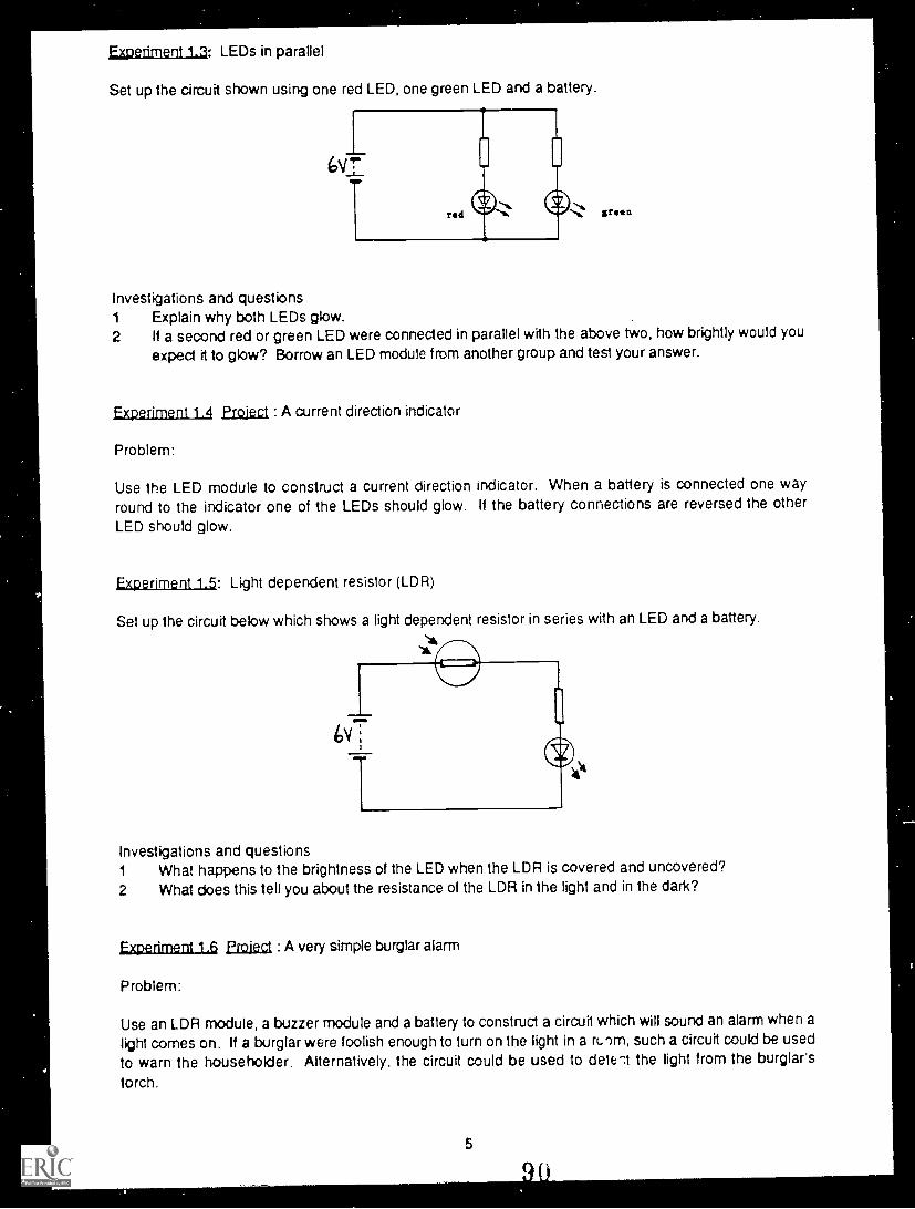
Experiment 1.3' LEDs in parallel
Set up the circuit shown using one red LED, one green LED and a battery.
8
green
14
e
Investigations and questions1 Explain why both LEDs glow.2 If a second red or green LED were connected in parallel with the above two, how brightly would you
expect it to glow? Borrow an LED module from another group and test your answer.
Notes
(1) This experiment is included to reinforce earlier circuit board work on parallel circuits and to introduceLEDs of different colour.
(2) Two LEDs of the same colour connected in parallel will glow with the same brightness because thecurrents through each are equal. This, of course, assumes that the series resistors are equal (which theyare on the LED module). An LED of different colour with the same value of series resistor may not glowwith the same brightness. Measurements with a milliameter would in fact show that the currents throughred and green LEDs with equal series resistors are almost exactly the same. Variations in apparentbrightness are due to differences in the materials used to construct LEDs of different colours, and tovariations in the sensitivity of the eye to different colours.
(3) It is important that pupils should be able to trace the current paths from the battery through eachbranch of a parallel circuit. For this experiment the path from the battery through each resistor and LED isshown below.
11
(4) The above experiment can be used to introduce the concept of positive and negative supply rails, asthe diagram below shows.
positive supply rail
negative supply rail
Experiment 1.4 Project : a current direction indicator
This is the first of a number of projects of varying complexity which pupils should tackle during theirelectronics work. A problem is presented and pupils attempt to solve it with guidance from the teacher. Inthe present case the problem is very simple and little guidance should be necessary.
Problem:
Use the LED module to construct a current direction indicator. When a battery is connected one wayround to the indicator one of the LEDs should glow. If the battery connections are reversed the otherLED should glow.
9 1 r_J
Solution:
Experiment Light dependent resistor (LDR)
Set up the circuit below which shows a light dependent resistor in series with an LED and a battery.
Investigations and questions1 What happens to the brightness of the LED when the LDR is covered and uncovered?
2 What does this tell you about the resistance of the LDR in the light and in the dark?
Nktabi
(1) The circuit diagram symbol for an LDR is shown in the diagram above.
(2) The current will flow in either direction as with an ordinary resistor. However, the resistance of an LDR
is very high in the dark (perhaps a million ohms or more) but falls to a low value (typically one or two
hundred ohms) in bright light.
(3) LDRs are known by a variety of different names. Cadmium sulphide cell or resistor is common (most
LDRs are made from this substance), as is the term photocell. For simplicity and to avoid confusion with
cells in batteries, teachers are advised to use only "light dependent resistor'.
1016
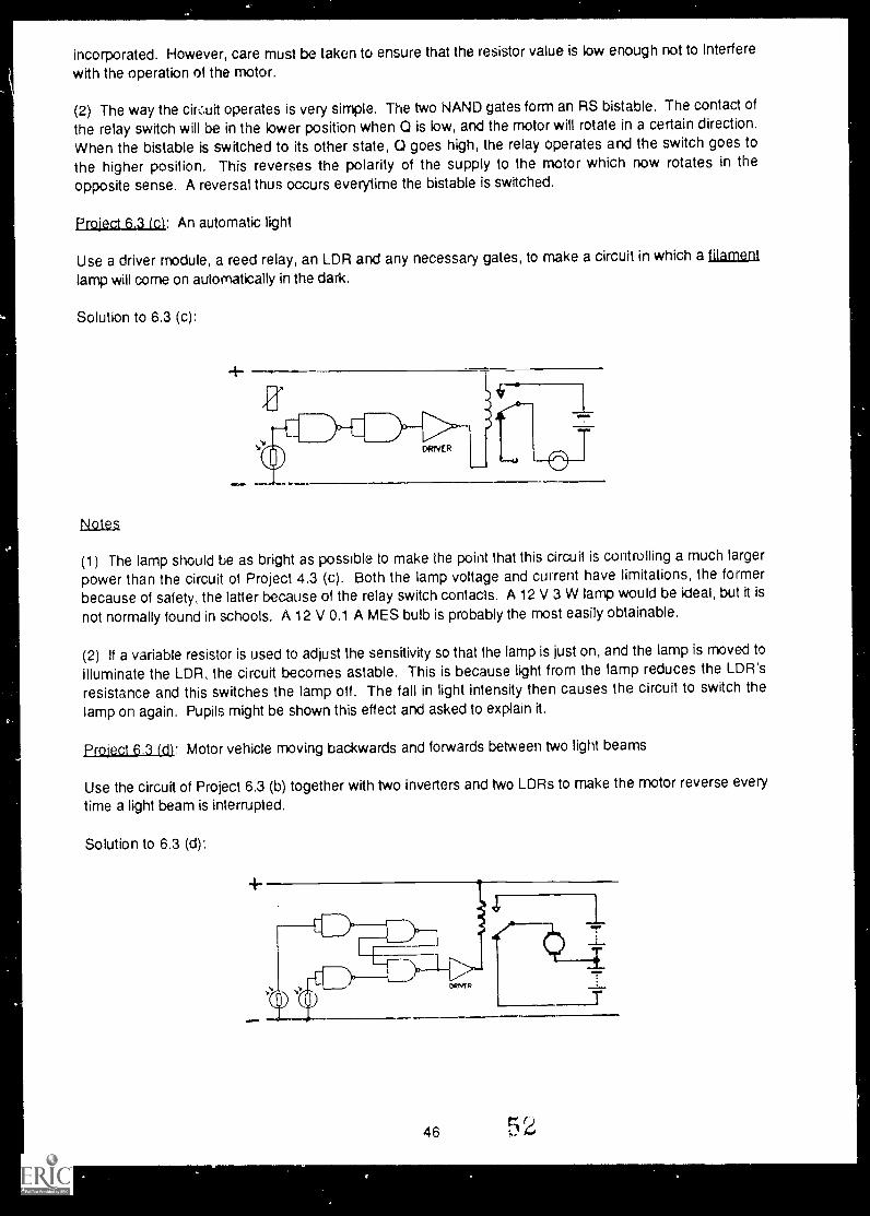
Experiment 1.6 Project : a very simple burglar alarm
The problem is to use an LDR module, a buzzer module and a battery to construct a circuit which willsound an alarm when a light comes on. If a burglar were foolish enough to turn on the light in a room, sucha circuit could be used to warn the householder. Alternatively, the circuit could be used to detect the lightfrom the burglar's torch.
Solution:
This is the first of a series of burglar alarm circuits appearing in the course. Alarms of increasingsophistication are constructed.
Note that the buzzer is likely to be a device with a definite polarity (in other words, current will pass throughit in one direction only). If no sound is emitted when the LDR is illuminated, reverse the connections tothe buzzer module.
11
1
SECTION 2. SWITCHES
Experiment 2.t Manual control of an LED
Connect a battery, an LED and a push-button switch together in a series circuit. Test whether you have
done it correctly by pressing the switch and then releasing it. The LED should light only when the switch
is pressed.
1 Draw a circuit diagram for this experiment.
2 Explain how the push-button switch works.
Notes
(1) This gives practice in drawing circuit diagrams. Pupils will need to know the symbol to use for ti.e
switch. They should be encouraged always to draw good, neat circuit diagrams.
(2) The circuit diagrams below are both correct.
Experiment 2.2: Reed switch and magnet
Take the reed switch module and examine the two metal contacts inside the glass envelope with amagnifying glass. These contacts are normally open. Now connect the switch in series with a buzzer and
a battery.
n ssit gne t
Ibuzzer
dvy
Investigations and questions1 Bring a small bar magnet close to the reed switch in the manner shown above. What happens?
2 What must have happened inside the glass envelope? Use your magnifying glass to see if you are
right.
Notes
(1) The reed switch consists of two metal contacts (called "reeds") inside a glass envelope filled with an
inert gas to prevent corrosion. Since the contacts are made of a ferrous metal (a metal containing iron),
they can be magnetised by a magnet. If the magnet is brought close to the switch in the manner shown
below, the metal strips are magnetised and attract.
121
/4slams envelope reeds
When the contacts close a current flows through the buzzer. There is no need to involve pupils in adetailed explanation of how the reed switch works. Direct experience of its switching action in thepresence of a magnet is all that is required.
(2) In this experiment a magnet is used to produce a force which closes the switch contacts. From theirearlier circuit board work, pupils will know that a current-carrying coil has a magnetic effect. In the nextexperiment pupils will meet a device in which switching is controlled by the magnetic effect of such a coilthe electromagnetic relay. The purpose of the present experiment is to bridge the gap between directmanual operation and electromagnetic control of switching. The progression is from direct manual controlto magnetic control, and then to electromagnetic control.
(3) Note that the reed switch contacts are either open or closed. Such a switch is called a single polesingle throw (SPST) switch. In the present case the contacts are normally open, and are shown as such inthe circuit diagram. This is in line with convention.
Experiment 2.3: Reed switch and coil - the reed relay
Using a reed relay module, set up the circuit shown below. Note that two separate battery supplies arerequired. Do NOT use either of the diode connections to the coil of the relay.
6v-r 1-4.v
investigations and questions1 What happens to the LED when the switch is closed?2 Try to explain why this happens.3 Now change the switch connections at the relay so that the LED is on until the push-button switch is
pressed.
Notes
(1) The relay uses a 'change-over' reed switch, also called a single pole double throw (SPDT) switch.Teachers should explain how it works. A ) c
The reed C and contact A are made of magnetic metal; contact B is a non-magnetic metal. C is normally incontact with B, but when a magnetic field magnetises A and C, they are attracted together so that contactwith B is broken and C contacts A instead. C springs back to its original position when the field is removed.In this course the reed switch in the relay is shown as below.
13
19
tr
(2) This is an important experiment since it introduces the electromagnetic relay. If a current flows through
the coil, the reed switch changes over and the LED lights.
(3) The important points to appreciate are (a) the switching is now determined by the flow of an electric
current, (b) although the two circuits are separate, what happens in one is controlled by what happens in
the other.
(4) In practice the current through the coil, which is needed to operate the switch, is usually far smaller
than the current which is allowed through the switch contacts themselves. So if the LED and resistor were
replaced by an electric motor requiring a large current to make it rotate, it could be operated by a much
smaller current passing through the coil circuit. This principle is important in electronics, and there are
other devices which provide the same capability (the transistor, for example). The particular case of motor
control appears in experiment 2.4 and in later experiments.
Experiment 2.4 The reed relay used to control a motor
Use the LDR module, the reed relay, the motor module and two batteries to set up the circuit below.
Investigations and questions1 What happens when the LDR is covered and uncovered? (You may have to shine a torch on the
LDR when you have uncovered it.)2 If possible, use ammeters to measure the current flowing from each of the batteries in the circuit
when the motor is running.3 Now connect the LDR module, the motor module and one battery as shown below. What happens
this time when the LDR is covered and uncovered?
4 Try to explain why it was necessary to use the reed relay in the lirst circuit.
Notes
(1) When the LDR is covered, its resistance is high, and not enough current flows through the relay coil to
operate the reed switch and switch the motor on. When the LDR is well illuminated, its resistance
becomes low and the relay operates.
14
(2) Ammeters (1A) placed in series with the coil and with the motor will show that the current through themotor (perhaps 0.2A) is a lot more than the current through the coil (a few milliamps). In other words, theflow of a small current is being used to control the flow of a much larger current - an important use of therelay. Of course more sensitive ammeters could be used.
(3) If the reed relay is not used, the change in the resistance of the LDR is not enough to allow the motorto operate. The relay is necessary for the reason given above.
(4) Electric motors require a relatively -rge current. If pupils leave them running for a long time, thebatteries become exhausted..
Experiment 2.5' The reed relay with coil and contacts in parallel (using a single power supply)
Connect up the circuit shown below.
Investigations and questions1 What happens to the motor when the switch is closed?2 In this circuit the relay coil and the relay contacts are connected in parallel. Copy the diagram and
mark on it the closed current paths from the battery, through each branch of the circuit and back tothe battery again.
Notes
(1) This circuit uses the concept of positive and negative supply rails first mentioned in Experiment 1.3.
(2) In experiment 2.4 (and 2.6), a small current in one circuit controlled a much larger current in anothercircuit which was completely separate with its own power supply. In the present experiment, a currentthrough one branch of a parallel circuit (the coil branch) controls a much larger current through anotherbranch (the motor branch). There is only one battery. This latter principle is introduced here because it isfundamental to the operation of the relay module introduced in the next section. If pupils meet transistorsin later work , they will again see this same principle in action.
Experiment 2.6 Project : automatic washing line
The problem is to use two batteries, the reed relay module, the electric motor module and the rain sensorto make a circuit which switches on an electric motor when rain falls. Such a circuit could be used as thebasis for an automatic washing line.
Solution:
rain sensor (swill Ntroboard
strip
915
Notes
(1) The rain sensor can be made from a small piece of stripboard on which are six copper strips connectedin the way shown below. If any of the strips are bridged by a conducting solution, the two leads are shortcircuited. This allows current to flow through the relay coil.
leads
(2) This experiment will not work with ordinary tap water. However, if a pinch of salt is adriAd the waterbecomes an excellent conductor and the necessary short circuit is provided. Alternatively, see note (3)below.
(3) Rain water conducts electricity, but not sufficiently to operate the reed relay in the above circuit.However the experiment will work with rain if the copper strips are covered by dry blotting paper which hasbeen previously soaked in a solution of salt in water. The salt solution is made simply by adding plenty oftable salt to tap water and stirring well. After immersion in the solution, the blotting paper should be driedthoroughly and taped so that it covers the copper strips. If rain falls on the blotting paper, the salt rendersit conducting and the necessary short circuit is provided.
Experiment 2.7 Project: Reversing an electric motor
The problem is to use a push-button switch, the reed relay and three batteries to make a circuit so that thedirection of rotation of the motor is reversed when the switch is pressed. Pupils should first draw a circuitdiagram and show it for approval.
Solution:
Notes
_L.
T
11Lcil"
(1) Pupils will probably find the need for 3 batteries confusing and care is needed to ensure their correctconnection.
(2) The number of batteries required can be reduced to one if a 3V motor is used.
16 2 2
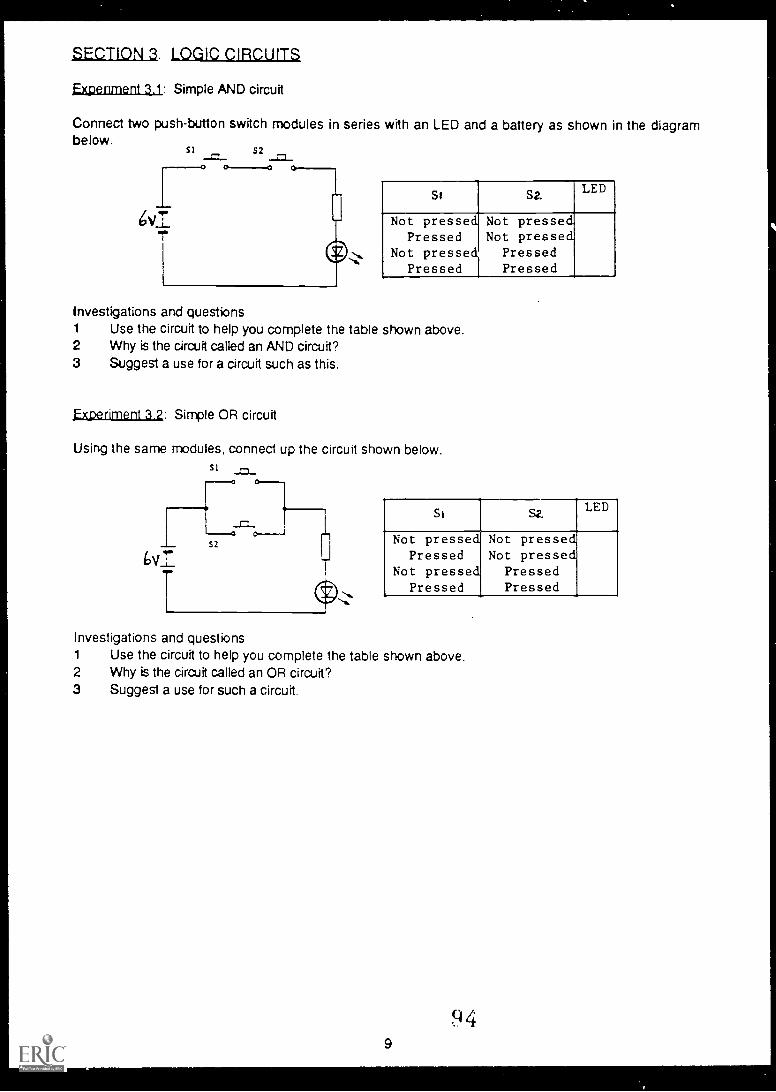
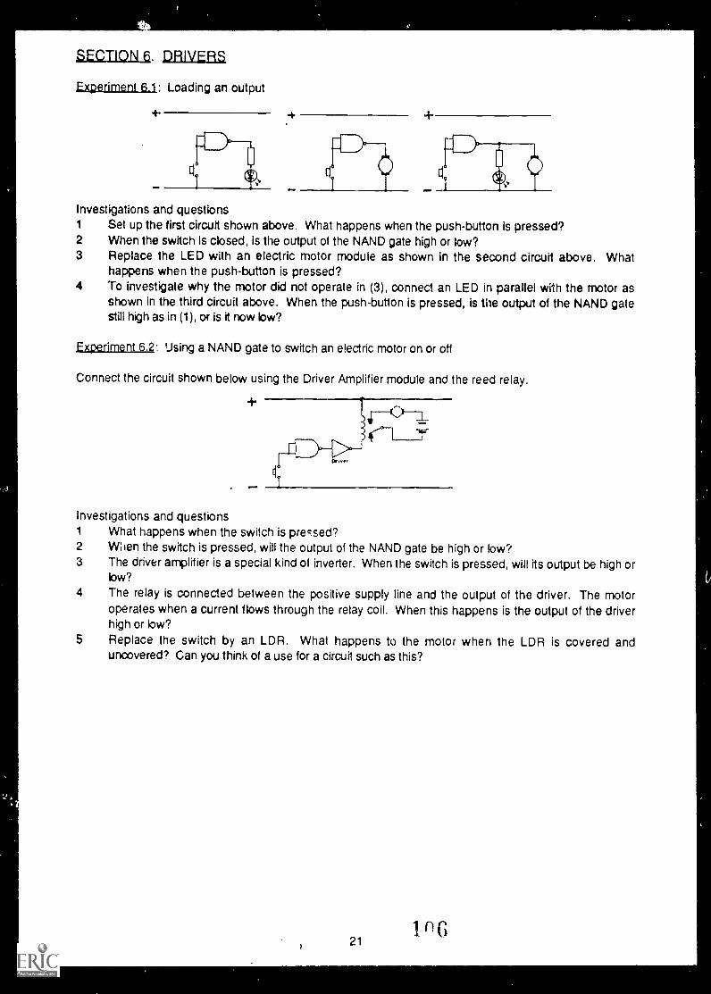
SECTION 3. LOGIC CIRCUITS
Experiment 3.1 Simple AND circuit
Connect two push-button switch modules in series with an LED and a battery as shown in the diagrambelow.
brr
L
t0_0St S2 LED
Not pressed Not pressedPressed Not pressed
Not pressed PressedPressed Pressed
Investigations and questions1 Use the circuit to help you complete the table shown above.2 Why is the circuit called an AND circuit?3 Suggest a use for a circuit such as this.
Notes
(1) The above circuit is a simple example of an AND circuit, and the table which pupils complete is knownas a "truth table". A truth table is a useful way of summarising the behaviour of the circuit. In this case, thetable tells us that the LED is on when S1 AND S2 are pressed. This is why the circuit is called an ANDcircuit.
(2) There are many situations in which such a circuit might be useful. For example, in a motor car we mightwant the ignition light to come on (indicating the car can be started) only when the driver has engaged hissafety belt AND closed his door.
Experiment 3.2; Simple OR circuit
Using the same modules, connect up the circuit shown below.
S, SL LEj>Not pressed Not pressed
Pressed Not pressedNot pressed Pressed
Pressed Pressed
Investigations and questions1 Use the circuit to help you complete the table shown above.2 Why is the circuit called an OR circuit?3 Suggest a use for such a circuit.
17 23
Notes
(1) This time the circuit is an example of an OR circuit, and the completed table is the truth table for an OR
circuit.. It tells us that the LED is on when either S1 OR S2 (or both) is pressed.
(2) An obvious use for such a circuit is as a simple burglar alarm. It is possible to purchase pressure pads
for home security systems which are really no more than a normally open SPST switch. A pad is placed
under a carpet near a door so that the switch is closed by the pressure of an intruder's foot. The above
circuit could be used with two such switches to protect two doors. An alarm would sound (replace the LED
by the buzzer) if entry was through door 1 OR door 2.
Experiment 3.3; Relay as a NAND circuit
Using the reed relay module, an LED and a battery, set up the circuit shown. Take great care inconnecting up the relay. Note that the polarity of the battery must be as in the diagram.
co r Pu-r
INPUT 1
2.INPUT-'
AOUTPUT
LOW LOW
LOW HIGH
HIGH LOW
HIGH HIGH
NANG,
Connect leads to the diode input terminals of the relay module, A and B. When the other end of one of
these leads is connected to the positive supply rail we say that the particular input is HIGH. If the lead is
connected to the negative supply rail, the input is said to be LOW. The output is HIGH if the LED is on and
LOW if the LED is off.
Investigations and questions1 By connecting the inputs high and low complete the truth table for the NAND circuit.
2 Try to explain why the output is high when one or both of the inputs is low. (HINT: consider whether
an input has to be high or low for a current to flow through the relay coil.)
3 Why do you think a diode is used at each of the two reed relay inputs? (HINT: consider what would
happen if input A were high and input B were low in the absence of diodes.)
dotes
(1) In electronics, a logic circuit is a switching circuit in which the state of the output at any instant depends
on the present state of all the inputs. The output is high only for certain input combinations.
(2) If the logic module were an AND circuit one would expect its output to be high when input A AND input
B were high, as in the left-hand truth table below. In fact the output is tut when input A and input B are
high. The module behaves as a NAND circuit (a contraction of negative AND). Its truth table is exactly the
inverse of that for an AND circuit (see the second truth table below).
AND c,....c.;e AIAND relay module
INPUT
LOW
LOW
HIGH
HIGH
INPUT
AOUTPUT
LOW
HIGH
LOW
HIGH
LOW
LOW
LOW
HIGH
18
INPUT
BINPUT
AOUTPUT
Low LOW HIGH
LOW HIGH HIGH
HIGH LOW HIGH
HIGH RIGA LOW
(3) NAND circuits are the most commonly found circuits in modern electronics, and this is one reason whythis particular circuit has been chosen for use in the rest of the experiments in this course. Other logiccircuits can be constructed using NAND circuits.
(4) The operation of the circuit is easy to understand. The first thing to note is that the contacts at theoutput form an SPDT switch: the pole of this switch is normally connected to the negative supply rail, thatis the output is low. This Is the position at the output when there is no current through the relay coil.When ether or both inputs are taken low current flows through the coil and the output contact changesover. The output goes high and the LED module is connected directly to the positive supply rail.
(5) Note that no current can flow through an input if it is high. This is also the case if the input is totallyunconnected or "floating". In electronics jargon this would be expressed by saying that the input floatalajcb. All that is meant by this is that an unconnected input behaves as though it were high.
(6) Diodes must be included at the inputs for an obvious reason. If there were no diodes and one inputwere taken high and the other low, there would be a direct short circuit across the battery. The diodesprevent this condition from arising.
(7\ Note that this circuit uses a number of concepts developed in earlier work, including the use ofpositive and negative supply rails and the actions of relays, SPDT switches and diodes. This systematicdevelopment of concepts is in line with the general philosophy of the course.
(8) The NAND relay circuit is constructed with its coil and contacts in parallel with the supply, and its inputsand output are either high or low. In these respects it is similar to electronic logic circuits constructed fromtransistors or available in integrated circuit form. The use of a relay as a logic circuit is therefore a soundintroduction to modern digital electronic circuits.
Experiment 3.4 A simple burglar alarm
Connect up the circuit shown. Take care to make the supply rails the correct polarity.
NRrlp CZ-re-LA.1k
Investigations and questions1 What happens when switch A or switch B is pressed (or both are pressed together)?2 Explain why this happens.3 How would you modify this circuit so that the alarm sounded either when a switch was closed or
when a light was shone on a LDR?
Notes
(1) This circuit is again more realistic if pressure pads are used instead of the switch modules (see Note 2of Experiment 3.2).
(2) The alarm can be triggered by a light beam (the burglar's torch) simply by replacing one switch moduleby an LDR module. If the LDR is covered (or the room is dark) it will have a very high resistance and virtuallyno current can flow through the relay coil. When light falls on the LDR its resistance rapidly falls to a lowvalue and current can flow through the coil, and the LDR thereby operates the relay (the input is now low).
19
Experiment 3.5; NAND circuit as an inverter
Connect an LED to the output and a flying lead to one of the inputs of the NAND circuit.
6v
1/4 vER:reft
OUTPUT
LOW
Investigations and questions1 Use the flying lead to take the input high and low and then complete the table above.2 In terms of the currents flowing through the coil and the LED, explain the completed truth table.
Notes
(1) When only one input of a NAND circuit is used (or the two inputs of a NAND circuit are joined togetherand treated as a singe input), it behaves as an inverter. Inverters will be used extensively in the restof the
course.
(2) It follows therefore that when the input is high, the output is low. When the input is low, the output ishigh.
Experiment a& Group experiment: Making an AND circuit
Using two NAND circuits (one as an inverter), an LED and a battery, set up the circuit below. Connect aflying lead to each input terminal of the first NAND circuit.
ra taas-r- 9. u 7'
A Z---- OM i'l'i
L :7__ ..1L _ _ _.1_1 $,4x
mai.9 tem I
wir i
Investigations and questions1 By connecting the inputs high and low,complete
the table. Does it behave as an AND circuit?2 Compare the table for this circuit with the table for
the circuit cf Experiment 3.3 (the NAND circuit).What has the inverter done?
3 Remove the flying lead from input B and connect a push-button switch between input B and the
negative supply rail. Connect the flying lead from input A to the positive supply rail (i.e. high), and
then operate the switch several times. Now connect the flying lead from input A to the negative
supply rail (i.e. low), and operate the switch. Can you see why the circuit is sometimes called a gate?
iN V I 121" K 12
INPUT'?
ININPUT OUTPUT
low I lowlow highhigh low
high , high
20
Notea
(1) The explanation of how this circuit operates is given in the notes to Experiment 3.3. The inverter
inverts the output of the NAND circuit.
(2) When the lead from input A is connected to the positive supply rail (i.e. high), operating the switch
connected to input B causes the LED to go on or off (i.e. the output follows the changes at input B).
When input A is low, the LED is off and operating the switch has no effect on it. The action of the circuit
can be likened to a gate (hence the name). With input A high, the gate is opened and the signals pass
through it; with input A low, the gate is closed and the output is not affected by changes at input B.
Experiment 3.7 Group experiment (Optional): Detection of an object of a length greater than a specified
maximum
Use two NAND circuits (one connected as an inverter), two LDR modules and a buzzer to connect up the
circuit below. Each LDR should be illuminated with a light beam. (Such a circuit might be useful to reject
overlong objects passing along a conveyor belt in a factory.)
6v".
1t
L_JN414 D 114V42-1.-E R.MOM
Investigations and questions1 What happens when you shade one or both of the LDRs?
2 The buzzer sounds only when both the LDRs are shaded. Try to explain why.
3 If objects of greater length than the distance between the LDRs pass in front of them, the buzzer
sounds. Where might this circuit be useful?4 How would the circuit behave if the inverter were left out and the buzzer connected to the output of
the NAND circuit?
Notes
(1) When light shines on the LDRs their resistance is low. The inputs of the first NAND circuit are
therefore low, so its output must be high. The second NAND circuit is an inverter, so its output is low and
the buzzer does not sound. if one of the LDRs is covered (but not the other), one of the inputs is still low,
a current still flows in the coil, the output of the first NAND circuit is still high, the output of the inverter is
low, and nothing happens.
But if both LDRs are covered, the output from the first NAND is low, so that the output from the second is
high and the buzzer sounds.
(2) A more realistic set-up can be achieved by fitting tubes over the ends of the LDRs and illuminating
them with "pencil" torches.
eardbesN tilos
LDS
41. taus Ire tvftaa "<gin,hue
21
7 p4
(3) Note that the two relay modules (a NAND circuit followed by an inverter) are together acting as an ANDcircuit. In other words, the output is high (the buzzer sounds) only when input 1 AND input 2 are high.
The work with the reed relay NAND circuit might conclude with a demonstration of two NAND circuitsconnected together as a bistable.
Experiment 3.8 Demonstration (Optional): Two NAND circuits as a bistable
tJA rsil) REp ua l 2 CREEP.'
To demonstrate the circuit, first press 'RESET' and show that the green LED is on, the red LED is off. Nowpress 'SET', when the circuit 'switches over' to red LED on, green LED off. Continued pressing of 'SET'has no further effect. Finally press 'RESET' again (and several times) when the circuit 'switches back' tothe original state.
Notes
(1) This experiment introduces a useful electronic circuit known as the "bistable". When the RESETswitch is pressed the output of NAND circuit 2 goes high and the output of NAND circuit 1 is low. Whenthe SET switch is pressed the output of circuit 1 goes high and the output of circuit 2 goes low. Thebistable circuit has two stable states. One stable state is when the output of 2 is high and the output of 1 islow (the RESET state). The second stable state is when the output of 1 is high and the output of 2 is low(the SET stale).
(2) After the SET switch has been pressed, further depressions of this same switch have no effect. Thesame is true of the RESET switch. This is an important property of the bistable.
(3) Note that the SET and RESET inputs are normally unconnected (they float high). To change from onestable state to the other the appropriate input must be taken low briefly.
(4) The operation of the circuit is quite easy to follow in terms of current flow through the coils and theconnections between the two NAND circuits. However, it would be unwise to dwell on these explanationswith pupils who find them confusing.
Explanation of the circuit
The two NAND circuits are joined together as shown. The circuits share the same power rails.
22
9')
The output C of the first circuit is connected to the input D of the second circuit. Similarly the output F ofthe second is connected to the input A of the first.
A red LED is connected between C and M. If C is high, the LED will light; if it is low, it will not.
A green LED is connected between F and N. If F is high, the LED will light; if F is low, it will not.
The important thing is that if C is high, the red LED is lit, D will be high and F will be low and the green LEDwill be out. As F is low, A is low, so C remains high. This is one of the stable states.
Similarly if C is low, the red LED will be out, and D is low. F will then be high, the green LED will be lit. A willbe high, so that C remains low. This is the second stable state and hence the name BISTABLE as it hastwo stable states.
The significant connections in a bistable are
the output of the 1st module is connected to the input of the 2ndthe output of the 2nd module is connected to the input of the 1st.
In order to set the bistable in one stable state or the other, push-button switches are connected betweeninput B and the negative rail (say, at P) and between input E and the negative rail (say, at 0). When thefirst push-button switch is pressed, a current flows through the relay coil and C becomes high and the redLED is lit and we have the first stable state. If however the second push button is pressed, F would behigh, the green LED is lit and we have the other stable state.
Pupils may have noticed that the circuit is ideal for the control of simple traffic lights since the red light andthe green light cannot be on together. Further simple demonstrations of its use can follow immediately.
Experiment 3.9 Demonstration (Optional): A latched burglar alarm
Replace the red LED in the circuit of Experiment 3.8 with a buzzer. Remove the green LED. If the buzzersounds, press the 'reset' switch to silence it.
The 'set' switch is now the 'trip' switch of the alarm. If it is pressed, the alarm sounds and it cannot beturned off by releasing the 'trip' switch or pressing it again. We say the output is "latched" the bistable islocked in its second stable state. The alarm can only be turned off by pressing the 'reset' switch. Thelatched nature of the alarm makes rt far more effective than the version constructed in Experiment 3.4.
Experiment 3.10 Demonstration (Optional): Using a bistable to control an electric motor
Remove the buzzer from the circuit of Experiment 3.9 (or both LEDs from the circuit of Experiment 3.8)and connect the motor between the outputs of the two NAND circuits (C & F in the diagram on p 22).
Pressing the 'set' and 'reset' switches alternately changes the direction of rotation of the electric motor.The bistable circuit here is used simply to reverse the polarity of the motor supply.
Much cheaper, more convenient and more versatile ways exist for producing bistable circuits by usingmicro-electronic logic circuits. Work with these circuits is in Part 2 of the course.
23?
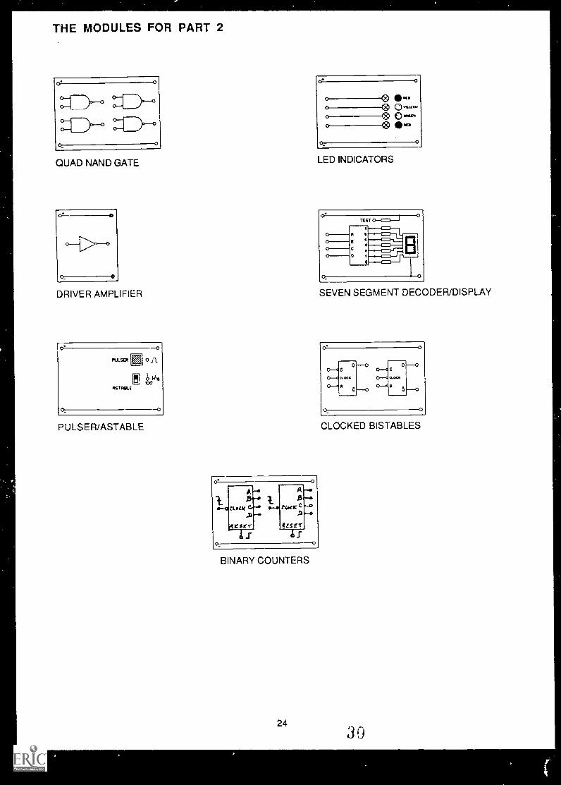
THE MODULES FOR PART 2
o C 0'
l.410""e'
o 0o 0
OMMIN0 0"0
CO_ O
QUAD NAND GATE
o' e
---->---
o e
DRIVER AMPLIFIER
0.
MASER7, 0 n5 ,i014.
ROAM
O
PULSER/ASTABLE
BINARY COUNTERS
24
LED INDICATORS
SEVEN SEGMENT DECODER/DISPLAY
C.
O 0
CLOCKED BISTABLES
39
Introduction to Part 2
This part of the course has been divided into six sections as below.
Section 4 : Electronic logic circuits - logic gatesSection 5 : The bistable circuitSection 6 : DriversSection 7 : CodingSection 8 : The pulser, the astable and the clocked bistableSection 9 : Counting circuits
Timing
The work can be conveniently covered in three years if Sections 4, 5 and 6 are taken together in the firstyeaf, S-ecrons 7 and 8 in the second year and Section 9 in the third year. If teachers wish to cover theground in only two years, then Sections 4 to 6 form a suitable group for the first year, leaving Sections 7 to9 for the second.
Pupils' backgrounds
The work described follows naturally from Electronics, Part 1. If pupils have not followed that course,the introductory work described in the first experiment will have to be approached in a different way andtaken more slowly.
The experiments
The course is essentially experimental. In this booklet, for each experiment there is a 'worksheet' togetherwith 'investigations and questions' for the pupils to consider. These are followed by 'notes' written forteachers to help them weave in any teaching which may be required. These notes also include somebackground information which may be useful in answering questions. The worksheets are reproduced,without the notes, in Electronics : Worksheets, Parts 1 & 2.
Projects
Most sections finish with 'Applications" in which electronics is put to use. Pupils and/or teachers are ableto select from a number of experiments which pose a problem, and pupils are invited to apply theirknowledge to find solutions. These problem-type experiments have been called Projects. The pupils'booklet Electronics : Worksheets, Part 2 lists the projects without solutions.
Clearly the time spent on projects must be limited, and it is suggested that, as a general rule, pupils shouldattempt two in each case. The wise teacher will make sure that each group starts with an easy one, for it isbetter to succeed with one than fail to solve two. Teachers will need to give help and encouragement inthis work without immediately revealing the 'correct' circuit. Before making up any circuits, pupils shouldbe urged to think out a design on paper. And then, if their circuit does not behave as expected, to thinkout why before making any changes. There are useful hints in reference 6 of the Bibliography(Appendix A).
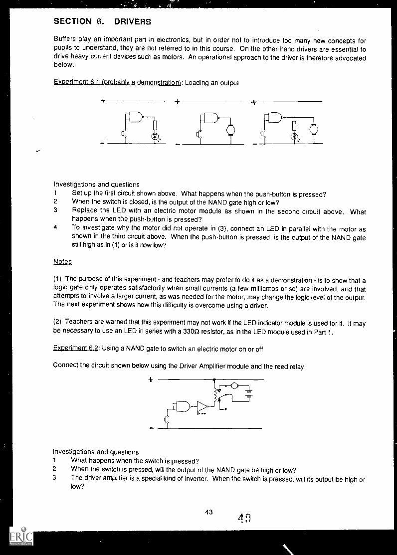
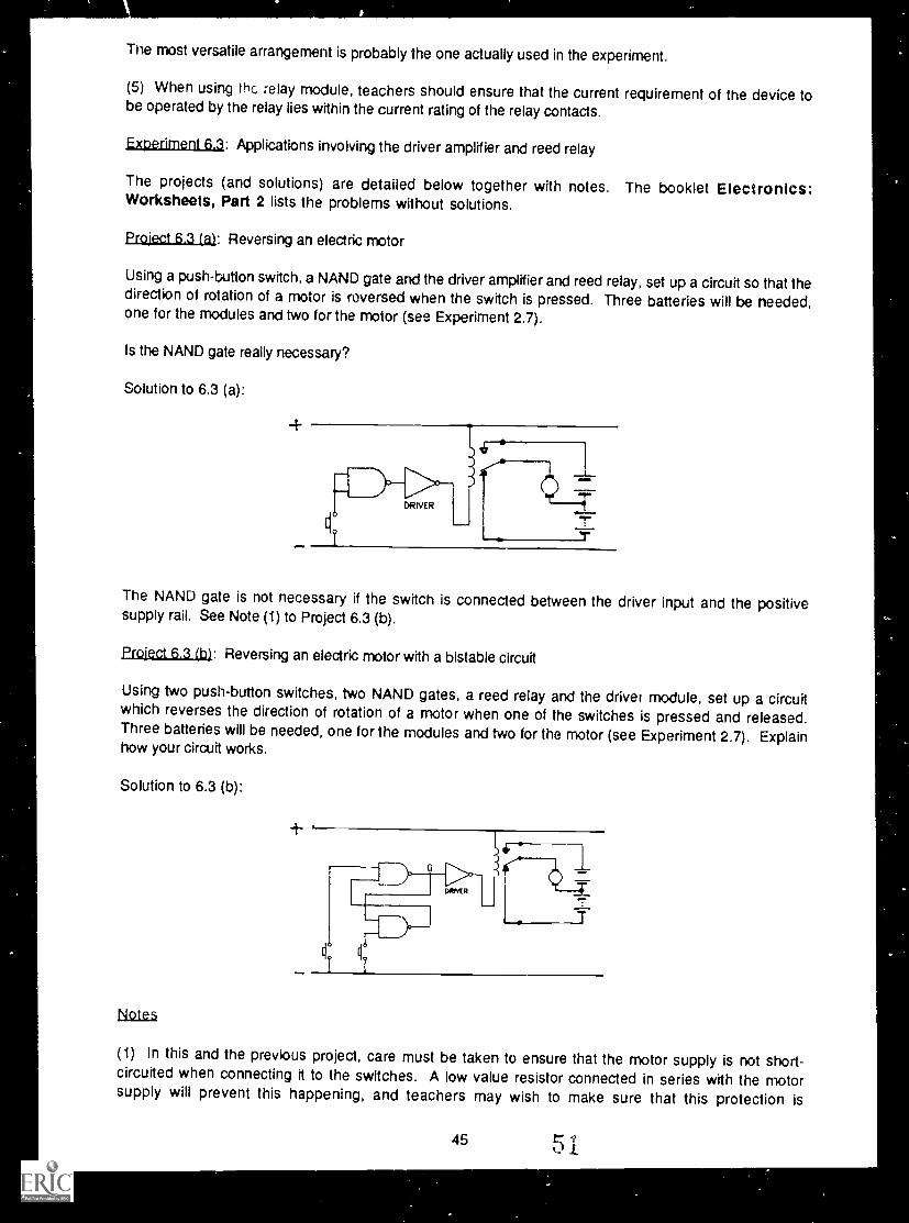
Power requirements for the modules using integrated circuits
A major advantage of CMOS integrated circuits is that they operate over a fairly wide "oitage range (3 V to18 V) and require very little supply current. Indeed, CMOS circuitry only requires significant current whendriving external devices such as LEDs and 7-segment displays. Dry cells capable of driving the LEDs andthe 7-segment displays are therefore a suitable power source since the current required will rarely exceed0.2 A.
25 3 t
The performance of CMOS integrated circuits (speed, drive capability, noise immunity) does vary with thesupply voltage chosen, but there is no space here to describe the technical details (interested readers arereferred to reference 2 in the Bibliography). Voltages near the centre of the allowed range are moresatisfactory than those near the limits. However, LEDs (and 7-segment displays) require resistors to limitthe current flowing through them, and the resistance value is dependent on the supply voltage used.Because 5 V or 6 V supplies are readily available to schools, the modules using LEDs have beendesigned for these supply voltages.
Using the modules module protection
Integrated circuits will be damaged if used with the supply polarity reversed. To protect the modulesagainst this possibility, a diode has been connected between the power rails of each module so that thediode conducts if the supply connections are inadvertently crossed (see the circuit diagrams at the end ofthis book). The reverse voltage is then about 1 V. A 3 A diode (IN5401) has been chosen for thispurpose since 3 A is the current, approximately, if any of the power supplies described above is short-
circuited. (In the case of the regulated 5 V supply, the 7805 regulator incorporates circuitry whicheventually results in the 7805 'closing down' (without damage) when it is short-circuited in this way.Clearly, other components in the supply circuits should also be able to carry a current of 3 A.)
In the experimental work, it will generally be necessary to connect two or more modules together. Tominimise the risk of damage, it is wise to cultivate the habit of always linking the corresponding power railsof the modules before connecting them to the supply. Other inter-modular connections can then bemade. It is also wise, when adding modules to a circuit, to disconnect the power supply whilst the additionis being made.
Set up the circuit shown below using the LED indicators module and a suitable power supply. Take careto connect the power supply correctly.
Now plug a lead into the top input socket of the Indicator module. The other end of this lead may beconnected to the positive power supply rail or to the negative power supply rail. Such a lead is called aflying lead. If connected to the positive rail, the input is said to be Ugh. If connected to the negative rail, itis said to be low.
Investigations and questions1 Find out how the top LED behaves when its input is connected first high and then low.2 Do the other LEDs behave in the same way?
Circuit diagrams
In the circuit diagram, an indicator is represented by the symbol below.
0
Using this symbol saves having to draw the LED and its associated circuitry every time we need to have anindicator in the circuit. That simplifies the diagram. Indeed, it will be necessary to simplify circuit diagramseven more, for they become difficult to understand and very tedious to draw when several modules arebeing used. To simplify further, the power supply is not drawn and only those parts of each module in useare included. The diagram above then simplifies to that below. Note that the + and signs near the powerrails show that a power supply is connected between them even though it has not been drawn.
experiment 42: The NAND gate
4,2 (a) Truth table
Set up the circuit shown below using one of the four NAND gates on the Quad NAND Gate module, andone of the LED indicators.
27
0 ® Q --®
O
3 t)
Make sure that the modules have their power supply rails linked correctly.
Each of the inputs A and B can be connected to the positive power supply rail (high) or to the negative
power supply rail (low) using a flying lead. The output is high if the LED is lit and Ism if the LED is unlit.
Investigations and questions1 By connecting the inputs high and low, complete the truth table
for a NAND gate.2 Does an unconnected input behave as if it is high or low?
3 Draw a simplified circuit diagram of the above circuit.
B A OUTPUT
LOW LOW
LOW HIGH
HIGH LOW
HIGH HIGH
4.2 (b) NAND gate as an inverter (NOT circuit)
Connect the two inputs of a NAND gate together as shown in the diagram below.
FLY NGE",(7 -0
O.%
INPUT OUTPUT
HIGH
LOW
Note that the two joined inputs can now be thought of as a single input. This single input can be taken
high or low using the flying lead.
Investigations and questions1 By taking the input high and then low, complete the truth table for the inverter (also known as a NOT
circuit).2 Instead of joining the two inputs of the NAND gate, connect one of them permanently high (or
simply leave it unconnected), and connect the flying lead to the other input. How does the circuit
now behave if the input is taken high and low? What happens if one input is tied permanently low?
4.2 (c) AND, OR and NOR gates from NAND gates
Connect the circuit shown below using two gates from the Quad NAND Gate module. Note that the
second NAND gate is connected as an inverter (NOT circuit).
OS.
B A OUTPUT
LOW LOW
LOW HIGH
)-±1(114 LOW
HIGH HIGH
Investigations and questions1 The above cimuit should behave as an AND gate. Check this by taking the inputs high and low, and
completing the truth table.2 Draw and complete the truth table for an OR gate. Compare this with the truth table for a NAND gate.
(You should notice that if every high input to the NAND gate became a low, and every low input a
high, it would give the OR gate you want. How can you change the inputs to the NAND gate? Clue:
you have just learnt about inverters.) Now design an OR gate using three NAND gates. Build the
circuit and check that it produces the correct truth table.
3 Draw the complete the truth table for a NOR gate. Use the remaining NAND gate on the module to
convert your OR gate to a NOR gate. Check that your circuit produces the correct truth table.
28
Notes
(1) The approach to logic gates adopted in the present experiment is appropriate for pupils who havepreviously followed Electronics, Part 1. Such pupils will have already met and used resistors, lightemitting diodes (LEDs), and light dependent resistors (LDRs). In addition, they will have been introducedto simple AND and OR circuits, and to the use of a relay as a two-input NAND gate. The truth tablessummarising the switching behaviour of these circuits will be familiar, and_this is why much of the work inthe present experiment is orientated towards cheQiiirist the properties of gates rather than an initialexploration. Integrated circuits were not used in Electronics, Part 1 so the practical context in whichpupils are using familiar concepts is now different.
(2) Pupils who have not previously followed Electronics, Part 1 will need some background in theareas mentioned above. An adequate preparation for the present course requires at least someexperimental work with LEDs, resistors and LDRs, as well as an introduction to truth tables.
(3) When introducing logic gates it is important that pupils should see as early as possible that thesecircuits have important practical uses. Pupils who have followed Electronics, Part 1 will already knowthat gates are useful. For those who have not seen gates performing useful tasks before, it would be agood idea to follow Experiment 4.2 (a) immediately with an application such as that in Experiment 4.3 (a).
(4) In Electronics, Part 1 pupils did not meet logic symbols. Before starting this experiment, they mustbe introduced to the symbol for a two-input NAND gate. The symbol used throughout this booklet is asbelow.
(5) It is vital to point out that in circuit diagrams using logic gate symbols, it is conventional to draw thesymbol without power supply connections. Some books, however, do show power supply lines joiningon to the symbol. The two methods are shown below for a NAND gate.
I
If the power supply lines were included in the circuit diagram for the third of the above experiments (ANDgate from a NAND gate followed by an INVERTER), it would appearas fc'
This latter method does have the advantage of emphasising the essential power supply connections tothe electronic devices inside the NAND gate, and teachers may wish to use it initially. Omitting powersupply connections does, of course, considerably simplify circuit diagrams and, once one is accustomedto the convention, makes them easier to read.
(6) Once the experimental work has been completed, the logic gate symbols for an inverter (the term NOTcircuit can now be used) arid for AND, OR and NOR gates can be introduced. Pupils should also be ableto write down the truth tables for each of these gates. In the case of AND, OR, NAND and NOT this will berevision of Part 1 work. The truth table for NOR should now be added. A summary of the above-mentioned logic gates is given below.
29 35
N D
A
B
B A OUTPUT
LOW LOW LOW
LOW HIGH LOW
HIGH LOW LOW
HIGH HIGH HIGH
OP
B A OUTPUT
LOW LOW LOW
LOW HIGH HIGH
HIGH LOW HIGH
HIGH HIGH HIGH
HAND
B
B A OUTPUT
LOW LOW HIGH
LOW HIGH HIGH
HIGH LOY? HIGH
HIGH HIGH LOW
HOP
>B A OUTPUT
LOW LOW HIGH
LOW MOH LOW
HIGH LOW LOW
HIGH HIGH LOW
The symbol for an INVERTER (or NOT circuit) is shown on the left below. As an inverter can be made from
a NAND gate, the second symbol below will also be used in this booklet.
C INPUT OUTPUT
HIGH
LOW
LOW
HIGH
Teachers should point out the presence of an inversion circle at the output of a gate with an inverting
function. So, for example, the output of a NAND gate is the inverse of that expected from an AND gatewith the same inputs. The same is true of a NOR gate when compared with an OR gate. Pupils shouldrealise that NAND and NOR are contractions of NOT AND and NOT OR, respectively. In terms of symbols,
is equivalent to
is equivalent to
(7) In the present experiment, NAND gates are used to make NOT circuits, AND, OR and NOR gates. One
reason for basing logic work in this course on the NAND gate is that the NAND gate can be used forinverting so that other gates can be built from it. This is also true of the NOR gate, but not of the AND gate
and OR gate. NAND gates and NOR gates can also be used to build bistable circuits, and this is another
reason why they are preferred to AND and OR gates. Both NAND and NOR gates are equally suitable asfundamental building bricks for an introductory course in digital electronics, but in the wider world of
electronics NAND gates are encountered more often and are probably the better choice.
(8) Note that a two input NAND gate can be used as an inverter in two ways (see question 2 of Experiment
4.2 b).C9N4r.1 TO POSIT FA SUPPLYOR LENA UNCONNECTED
The NAND gate module used in the present course has inputs which are high when unconnected. Thesimplest way to make an inverter is therefore to use just one input of a NAND gate and connect the other
to the positive rail or leave it floating. There is some advantage in using the NAND gate in this way. If the
two inputs are connected in parallel, the input capacitance is increased and the noise immunity is !hereby
greater. However, it seems to cause less confusion to pupils if the inverter is shown as in the diagram on
the left above, and that will be used in this booklet.
Further information concerning the behaviour of unconnected inputs of the NAND gate module are givenin the Appendix B Technical Details.
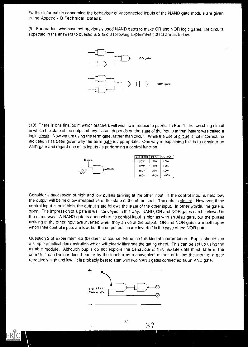
(9) For readers who have not previously used NAND gates to make OR and NOR logic gates, the circuitsexpected in the answers to questions 2 and 3 following Experiment 4.2 (c) are as below.
--0
OR gate
Do-ED--- NOR gate
(10) There is one final point which teachers will wish to introduce to pupils. In Part 1, the switching circuitin which the state of the output at any instant depends on the state of the inputs at that instant was called alogic circuit. Now we are using the term gate, rather than circuit. While the use of circuit is not incorrect, noindication has been given why the term call is appropriate. One way of explaining this is to consider anAND gate and regard one of its inputs as performing a control function.
CONTROL
JU-LWiUt
OUTPUT
CONTROL INPUT OUTPUT
LOW LOW LOW
LOW HIGH LOW
HIGH LOW LOW
HIGH HIGH HIGH
Consider a succession of high and low pulses arriving at the other input. If the control input is held low,the output will be held low irrespective of the state of the other input. The gate is closed. However, if thecontrol input is held high, the output state follows the state of the other input. In other words, the gate isopen. The impression of a pate is well conveyed in this way. NAND, OR and NOR gates can be viewed inthe same way. A NAND gate is open when its control input is high as with an AND gate, but the pulsesarriving at the other input are inverted when they arrive at the output. OR and NOR gates are both openwhen their control inputs are low, but the output pulses are inverted in the case of the NOR gate.
Question 2 of Experiment 4.2 (b) does, of course, introduce this kind of interpretation. Pupils should seea simple practical demonstration which will clearly illustrate the gating effect. This can be set up using theastable module. Although pupils do not explore the behaviour of this module until much later in thecourse, it can be introduced earlier by the teacher as a convenient means of taking the input of a gaterepeatedly high and low. It is probably best to start with two NAND gates connected as an AND gate.
31
3
When the control input is high, pulses will pass through the AND gate and the two LEDs will flash on andoff together. If the control input is taken low, the LED at the output will be permanently low. If a singleNAND gate is used and the control input is high, the output LED will flash on and off but it will be on whenthe LED at the input is off, and vice versa. When the control input is low, the output LED will bepermanently on.
Other gates can, of course, be investigated in the same way.
Experiment 4,3: Applications using NAND gates
The projects (and solutions) are detailed below together with notes. The booklet Electronics :
Worksheets, Part 2 lists the problems without solutions.
Notes
(1) An essential requirement of this course is to show how electronic circuits can perform useful tasks and
control devices such as LEDs, buzzers and motors. Pupils must also be encouraged to apply theirknowledge to circuit design and think out how combinations of gates will operate. To achieve these ends,they should be set problems to solve. Experiment 4.3 is a collection of such problems or projects.
(2) Time constraints will inevitably mean that it is impractical for all pupils to attempt all projects, though it is
hoped they will attempt two or three of them. Some of these are simple, other are quite difficult and pupils
may need a lot of help. Teachers will no doubt ensure that the projects chosen match the ability of theirpupils: it is better to succeed with a simple one than to fail with a difficult one. Perhaps a good approach is
to allow groups to select problems to work on, and then to have a plenary session in which solutions are
discussed and demonstrated.
(3) Some of the applications repeat the work of Part 1, but this time integrated circuit NAND gates areused rather than NAND circuit relays. Note that the circuits are identical whether relay or integrated circuit
NAND gates are used. This should facilitate the transition from relays to ICs.
(4) Note that these applications make extensive use of illuminated LDRs to hold inputs low. This isdiscussed in relation to module circuitry in Appendix B. As far as pupils are concerned, an LDR can simply
be regarded as a switch which is open in the dark and closed when illuminated.
It is worth emphasising to pupils that it is necessary to connect input devices such as LDRs between gate
inputs and the negative supply rail. Because an unconnected input floats high, an LDR connected to the
positive supply rail will not change the logic level at the input when the illumination changes. Connected
to the negative supply rail, an LDR will cause a low level input when brightly illuminated (low. resistance)
and a high level input when dark (high resistance).
A suitable LDR for the work in the present course is the popular ORP 12.
(5) Buzzers are also used extensively in this and later experiments. These are low current (a few mA) d.c.
devices which typically operate over a voltage range from, say, 3 V to 15 V. They emit a constant
frequency audible tone.
(6) Further suitable projects will be found in reference 6 of the Bibliography (Appendix A).
Project 4.3 (a): Burglar alarm (NAND application)
Use a single NAND gate, an LDR, a push-button switch and a buzzer to make a simple burglar alarm. Thealarm should sound when the LDR is illuminated (the burglar's torch) or the switch is closed (the burglar's
Use two NAND gates (one connected as an inverter) together with two LDRs and a buzzer to construct asystem which will sound an alarm when an object is longer than a specified maximum length. Such a circuitmight be used to reject overlong objects passing along a conveyor belt in a factory.
Solution to 4.3 (b):
The LDRs are positioned a distance x apart (where x is the specified maximum length of the object) andilluminated by "pencil" torches. The alarm sounds when both beams are interrupted.
Project 4.3 (c): Automatic night light
Use two NAND gates (both connected as inverters), an LDR and an LED indicator to make a circuit in whicha light (the LED) will come on automatically in the dark. A circuit of this kind would be useful to light up thedisplay in a shop window automatically when darkness falls.
Solution to 4.3 (c):
3339
(1) This application uses two NAND gate inverters to 'drive'an LED indicator. The circuit on the left above is not verysensitive to changes of light intensity. This is because theLDR and the internal circuitry of the NAND gate moduleeffectively form a potential divider between the supply rails(see right). As R has a high resistance, it needs a largechange in the resistance of the LDR to change the voltagelevel at the NAND gate input appreciably.
(2) The second circuit at the top of the page allows the sensitivity to be changed. The variable resistorshould be set so that the LED is on the verge of switching on. Then any darkening of the LDR will causethe LED to light. The value of the variable resistance to use depends somewhat on ambient lightconditions, but 10 IcS1 should suit most circumstances. It is important that pupils should meet the potentialdivider and teachers could demonstrate the right-hand circuit as an example of its use. If teachers chooseto introduce the potential divider as part of the work on Electricity, then this project might well be donethere and omitted here.
Project 4.3 (d): Fire alarm
Use a NAND gate connected as an inverter, a thermistor, a variable resistor and a buzzer to make a simple
fire alarm. The alarm should sound when the thermistor is heated.
How would you adjust the circuit so that the alarm sounded when the temperature reached a higher value?
Solution to 4.3 (d):
Notes
(1) It is important that pupils should have previously met the potential divider and the thermistor if they areto solve this problem.
(2) An inexpensive TH3 thermistor can be used for this fourth application. Its resistance at roomtemperature is about 40052, and decreases to about 2052 at 100°C. At room temperature, the 5 k.S2
variable resistor (a 5 IQ potentiometer connected as a variable resistor) should be set so that the buzzer isjust off. Warming the thermistor with the hand will then cause the buzzer to sound. To increase thetemperature at which the alarm responds, the value of the variable resistance should be decreased. Notethat a 2.5 kS2 variable resistor provides greater sensitivity in this application, but with care, a 5 k.Q or even a
10k12 value can be used satisfactorily.
Project 4.3 (el: Safety circuit for a safe
A safety circuit for a large safe sounds an alarm only if the door is closed but not locked. Closing the dooropens a switch, whilst locking the door Qloses another switch. What sort of logic gate is required to dothis? Set up the circuit and test it. Now adapt your circuit for a safe which has two locks.
34
Solutions to 4.3 (e):
+
This project introduces the 3-input AND gate which will be used in several projects later in the course.Note that if NAND gate 4 is omitted, the circuit is a 3-input NAND gate.
Project 4.3 VI: The skittle alley winner-indicator!
In a fairground skittle alley, customers try to bowl over three skittles. Each skittle stands on a small switchvhich it keeps closed until it is bowled over. Design a circuit which lights a lamp only when a customer is
successful.
Solution to 4.3 (f):
Notes
(1) This is a similar problem to that of Project 4.3 (e) but somewhat easier to think about. It can, of course,be introduced as a two-skittle problem first.
(2) The project introduces the 3-input AND gate which occurs in later projects. Note that if gate 4 isomitted, the circuit is a 3-input NAND gate.
Project 4.3 (g): Car doors warning light
Design a circuit which will cause a warning lamp on the dashboard of a two-door car to light if either of thedoors is not closed. Closing a door closes a switch.
Solution to 4.3 (g):
r
35
Project 4.3 (h): Circuit Investigation
This is a circuit to investigate rather than a problem to solve. In the truth table, '0' stands for 'low', and '1'
stands for 'high'.
BACDEF00011011
Investigations and questions1 Copy the truth table and complete it to show the voltage level at each of the lettered points for each
of the level combinations at A and B.2 Set up the circuit and check your predictions for the output F. If you have made an error, use a flying
lead from another LED indicator to check your predictions for the level at each of the points C, D and
E. Do this by touching the free end of the flying lead on to each of those points in turn.
3 Suggest a use for this circuit.
Note
The circuit is an exclusive OR gate. The correct truth table is as shown. Note that F is high when A j;d:B is
high, excluding the case when both are high.
BACDE00111001101,1101101110110
It is a "light at the top of the stairs" circuit.
3642
SECTION 5. THE BISTABLE CIRCUIT
Experiment 5.1: Making a bistable using two NAND gates
Set up the circuit shown below using two gates from the Quad NAND Gate module.
RESET
I
Investigations and questions1 First of all press and release the switch marked RESET. Which LED is on and which one off?
2 Now press and release the switch marked SET. What happens?3 Press and release the SET switch several more times. What happens?4 Now press and release RESET. What happens?
Circuit diagrams
Notice that the LED indicator connected to the output of NAND gate 1 is not drawn beneath the LED
indicator of gate 2, even though that is where it is placed on the indicator module. Circuit diagrams are
easier to understand if the parts are drawn in convenient places rather than as they are placed on the
modules. Notice too that the positive power rail is drawn in the above diagram even though no leads are
shown connected to it. Frequently such a power rail is omitted from circuit diagrams. However in this
course both power rails will be drawn to remind you that a power supply is needed to make the circuits
work.
Notes
;1) In Electronics Part 1, work with bistable circuits was optional. The bistable is such a vitally important
building block in digital electronics that all pupils must now meet it.
(2) Teachers are strongly recommended to start work on bistable circuits by quickly demonstrating,
without explanation, the action of a Jatched burglar alarm (see Experiment 5.2 (a)). This very clearlyillustrates the existence of two stable states in a way that pupils are not likely to forget. The usefulness of
such a circuit is also readily apparent. When they come to Experiment 5.2 (a) pupils will have to work out
how to use a bistable circuit to make this alarm themselves.
(3) The circuit of the present experiment behaves in the following way. When the RESET switch ispressed, the output of NAND gate 2 goes high and the output of NAND gate 1 is low. When the SETswitch is pressed, the output of NAND gate 1 goes high and the output of NAND gate 2 goes low. The
bistable circuit has two stable states. One stable state is when the output of 2 is high and the output of 1 is
low (the RESET state). The second stable state is when the output of 1 is high and the output of 2 is low
(the SET state).
(4) After the SET switch has been pressed, further depressions of this same switch have no effect. The
same is true of the RESET switch. This is an important property of the bistable.
(5) Note that the SET and RESET inputs are normally high. To change from one stable state to the other,
the appropriate input must be taken briefly low.
37 43
(6) Electronics Part 1 explained how a bistable circuit built from two NAND circuit relays worked. In thecase of integrated circuit NAND gates, teachers might like to use the following explanation.
Consider two NAND gates connected such that the output of one is joined to the input of the other. If thesecond input of each gate is not used, both gates act as inverters.
HIGH
FLYING
LEAD >
If the input of the first gate is made high, its output will be low (above left). The input of the second gate istherefore low and its output high. If the output of the second gate is now connected to the input of thefirst gate (dotted line above right), the original high input to the first gate provided by the flying lead canbe removed and the system will be in a completely stable state. The high output of the second gatemaintains the high input to the first gate.
A different situation arises if the flying lead to the first gate is originally tied low (below left).
NIGH Low L064LOW
Since the input of the first gate is now low, the output of the second gate is also low. If the output of thesecond gate is connected back to the input of the first gate, the original flying lead can be removed andwe again have a completely stable system. This time, however, the output conditions at the two gates arereversed.
So we see how a system consisting of two inverters can be connected in such a way that there are twostable states. However, for such a system to be useful, a means must be provided of switching betweenthese two states. The second (and so far unused) input of each NAND gate can be used for this purpose.
Consider the initial stable state shown in the above diagram. The inputs of the first NAND gate are bothhigh, and its output is, of course, low. But the SET switch is pressed, one input of the first NAND gate istaken low and so its output goes high. The output of the second gate therefore goes low and this lowstate is fed back to the other input of the first gate. If the SET switch is now released, the system is in thesecond completely stable state. Note that pressing the SET switch a second time has no effect. Thesystem can only be switched back to its original slate by pressing the RESET switch.
The line shown dotted in the earlier diagrams provides a positive feedback link. In other words, the outputof the system is fed back to provide an input of the same polarity.
(7) In electronics literature, the above bistable would usually be drawn as below.
38
The connections are in fact identical, but the gates are shown one beneath the other. Note that theoutput of the top gate (with the SET input) is usually labelled Q, and that of the other (with the RESETinput) is labelled Q.
0 and Q are often referred to as complementary outputs, meaning that each is the inverse of the other.
(8) The above diagram is rather cumbersome to use in circuit diagrams. A more convenient symbol incommon use is as follows.
The circles on the S and R input lines indicate that they are active low i.e. the S and R inputs are normallyhigh and must be taken momentarily low to have an effect (this notation to identify active low inputs isconventional in digital electronics).
In summary, this important bistable building block, which is often known as an RS bistable or as an RS flip-flop, has the following properties.
(a) There are two stable states: SET state (0 high, 5 low) and RESET state (0 low, (7) high).
(b) Normally the system will be in one of its stable states. In both states the S and R inputs will behigh.
(c) To change from the SET state to the RESET state the R input must be taken momentarily low, If
R is taken low again, nothing happens.
(d) To change from the RESET state to the SET state the S input must be taken momentarily low. IfS is taken low again, nothing Happens.
This behaviour can be summarised in a truth table, but pupils do r need to know how to do this. For thebenefit of teachers, the truth table is given below.
S P 0 0HIGH HIGH STAYS THE SAMELOW HIGH HIGH LOWHIGH LOW LOW HIGHLOW LOW DISALLOWED
Note that the state with both S and R low is disallowed, since both Q and TZI are then forced to go high atthe same time and the system will be in neither of its stable states. It is perhaps more accurate to say thatthis state is avoided rather than disallowed, although the latter term is frequently encountered.
(9) Teachers should make sure that pupils understand the difference between a bistable and a logic gate.After all, if we omit the Q output of the former, there are some surface similarities.
39
The key point is that a logic gate requires retention of its input signals to remain in a given state. The
bistable remains in a stable state when the inputs are removed (the particular state will depend upon which
input was last taken low).
pe riment 5.2: Bistable applications using NAND gates
The projects (and solutions) are detailed below, together with notes. The booklet Electronics:Worksheets, Part 2 lists the problems without solutions.
Project 5.2 (al: Latched burglar alarm
Use two NAND gates, two push-button switches and a buzzer to make a latched burglar alarm. One switch
should correspond to the "trip" switch. If this is closed (by the burglar's foot, perhaps) the alarm should
sound and stay on even when the switch is released or pressed again. The second switch shouldcorrespond to the"reset" switch, and would be hidden away in a place known only to the householder.
Only when this switch is pressed should the alarm be silenced.
Once you have built this circuit, convert it to an alarm which will come on and stay on when a light (the
burglar's torch) shines on an LDR.
Solution to 5.2 (a):
Notes
(1) Replace the "trip" switch by an LDR to make a light activated latched alarm. A variable resistor
connected between the LDR and the positive supply rail, to form a potential divider, will allow the
sensitivity to be adjusted (see 'Notes' to Project 4.3 (c)).
(2) With CMOS modules, the output of NAND gate 1 may be unable to drive both the buzzer and the input
to NAND gate 2. if this is the case, possible courses of action are (a) to use an LED indicator rather than a
buzzer, (b) to try "buffering" the buzzer by connecting it to the output of another NAND gate whose inputs
go to the output of NAND 2 in the circuit above.
(3) When the "trip" switch is pressed, the alarm sounds and cannot be turned off by releasing the switch
or by depressing it again. We say that the output is latched. The bistable is now locked in its second
stable state (the state with the output of the NAND gate connected to the buzzer high, and the output of
the other NAND gate low).
(4) The alarm can only be turned off by pressing the "reset" switch. In a practical system the trip switch
might be contained in a pressure pad of the type designed especially for home security systems. Such a
pad (effectively a normally open push-button switch) is placed under a carpet near a door so that the
switch is closed by the pressure of the intruders foot. Pressure pads of this kind are available.
40
Project 5,2 (b).: Latched fire alarm using a bistable
Build a fire alarm which, once triggered, will continue to sound until it is reset.
Solution to 5.2 (b):
See 'Notes' to Project 4.3 (d) for information regarding a suitable thermistor, and Note (2) of Project 5.2 (a)regarding possible problems with driving the buzzer.
Project 5.2 (c): Simple stop-go traffic lights
Traffic in a one-way street has to cross a bridge which can only have one car on it at a time. The bridge is tobe controlled by a set of stop-go lights, activated by switches in the road, so that the lights go red when acar enters the bridge and then green as the car leaves it. Design a circuit to do this job.
Solution to 5.2 (c):
Project 5.2 (d): Traffic lights operated by an SPST switch
REO
GREEN
A simple set of stop-go traffic lights is to be operated by an SPST switch so that either the red light is on orthe green light is on, but not both together. Design a circuit, using a bistable, which will do this.
Solution to 5.2 (d):
RED
GREEN
When 'set' is high, 'reset' is low and the green LED is on. Since both inputs to NAND gate 1 are high, thered LED is off. When 'set' is low, the red LED is on, and since both inputs to gate 2 are now high, thegreen LED goes off.
Project 521e1: Quiz master
A quiz master circuit is used to identity the first contestant to push his or her answer button in a quiz game.Each contestant has a push-button and an indicator light (in this case, an LED). The light of the firstperson to answer should come on and stay on. At the same time all other lights should be prevented fromcoming on.
41
To make such a quiz master is not easy, and you may need help from your teacher. Each contestant in the
game will need four NAND gates (two connected as a bistable), a push-button switch and an LEDindicator. The best approach is to wire up the four gates for one contestant, and then wire up the fourgates for another contestant separately. Finally connect the two sets together and see if your quiz master
works!
Solution to 5.2 (e) (for each contestant):
from 15 outputof other contestant
Note
B
to input B ofother contestant(Take tow to reset)
to nput A ofother contestant
The above application (the quiz master) is rather complex, and may be too difficult for the majority of
students to work out on their own. However, it is worth constructing a quiz master of this kind even if the
teacher has to explain its design. Pupils will have great fun playing with it, and the use of logic gates is
instructive.
The principle of operation is in fact quite simple. If the B inputs of the two quiz stations are taken low, the
bistable circuit formed by the two right hand gates will be reset. In other words, the Q outputs at the
stations will be high and the LEDs off.
Consider the station of one particular contestant. The A input will initially be high because it is connected
to the Q output of the other station (which has just been reset). The A input effectively "opens" the NAND
gate to which it is connected, so if this contestant is the first to press his or her switch, the bistable is set by
a low going pulse and the LED indicator comes on. At the same time 0 goes low, and since this output is
connected to the A input of the other station, the NAND gate controlled by this A input is "closed". This
means that a low going pulse from the other contestant's push-button cannot pass to his or her bistable.
The bistable therefore remains in the reset state with the indicator light off.
Simpler quiz master stations can be built using fewer NAND gates. However, they are unlikely to have the
required properties of simultaneously latching the victor's indicator LED and permanently disabling the
switches of all other contestants.
42d^
SECTION 6. DRIVERS
Buffers play an important part in electronics, but in order not to introduce too many new concepts forpupils to understand, they are not referred to in this course. On the other hand drivers are essential todrive heavy curient devices such as motors. An operational approach to the driver is therefore advocatedbelow.
Experiment 6.1 (probably a demonstration): Loading an output
Investigations and questions1 Set up the first circuit shown above. What happens when the push-button is pressed?2 When the switch is closed, is the output of the NAND gate high or low?3 Replace the LED with an electric motor module as shown in the second circuit above. What
happens when the push-button is pressed?4 To investigate why the motor did rot operate in (3), connect an LED in parallel with the motor as
Shown in the third circuit above. When the push-button is pressed, is the output of the NAND gatestill high as in (1) or is it now low?
Notes
(1) The purpose of this experiment and teachers may prefer to do it as a demonstration is to show that alogic gate only operates satisfactorily when small currents (a few milliamps or so) are involved, and thatattempts to involve a larger current, as was needed for the motor, may change the logic level of the output.The next experiment shows how this difficulty is overcome using a driver.
(2) Teachers are warned that this experiment may not work if the LED indicator module is used for it. It maybe necessary to use an LED in series with a 3300 resistor, as in the LED module used in Part 1.
:periment 6.a: Using a NAND gate to switch an electric motor on or off
Connect the circuit shown below using the Driver Amplifier module and the reed relay.
Investigations and questions1 What happens when the switch is pressed?2 When the switch is pressed, will the output of the NAND gate be high or low?3 The driver amplifier is a special kind of inverter. When the switch is pressed, will its output be high or
low?
43
4 The relay is connected between the positive supply line and the output of the driver. The motoroperates when a current flows through the relay coil. When this happens is the output of the driver
high or low?5 Replace the switch by an LDR. What happens to the motor when the LDR is covered and
uncovered? Can you think of a use for a circuit such as this?
Notes
(1) The function of a driver is to provide an interface between a device such as an integrated circuit which
is capable of controlling only a small current, and a device, such as a relay or an electric motor, which
usually requires a relatively large current for its operation.
(2) The simplest and cheapest inverting driver amplifier consists of a single transistor and one resistor.
However, pupils do r need to know anything about the way in which drivers are built. The transistor is
jag' part of the present course, and the following information is for teachers only.
+0 0
ZS an RVca
rvuT
A relay and its protective diode (essential when switching inductive 'oads) would then be connectedbetween the positive supply line and the transistor collector in the way shown. When the transistor input
goes high, the collector current flows through the relay coil into the transistor.
In practice, it is better to use two transistors connected as a Darlington pair. The current gain of such a
system is far higher than that of a single transistor, and the base current needed to switch the collectorcurrent on is then easily supplied by the high output of any integrated circuit.
(3) Note that the circuit diagram shows the motor being driven by a separate power supply. If separate
supplies are not available, the motor may be driven by the supply used for the modules, provided, of
course, that this supply is capable of delivering the necessary current. It is a wise precaution to connect a
1000 p.F capacitor between the power lines in those circumstances.
(4) In the present experiment the driver amplifier operates a relay which controls the motor. The same job,
of course, could be done in other ways.
In the circuit below on the left the relay is omitted entirely. This would be a satisfactory arrangementprovided the motor current does not exceed the maximum current allowed by the driver. One possibleproblem with this arrangement is that the motor and the logic circuitry share the same power supply. This
would certainly be a disadvantage with CMOS integrated circuits where only a small battery is needed for
the ICs. A motor would soon run this flat, or might not operate at all.
In the circuit on the right, the driver is omitted! Reed relays are available which will operate satisfactorily off
a low voltage supply with a coil current of only a few milliamperes, and these can be operated directly using
the logic gate output. However, a disadvantage of this type of relay is that the contact ratings are often
rather small, and could possibly overheat when used with a motor requiring a large current.
44
5u
11
The most versatile arrangement is probably the one actually used in the experiment.
(5) When using Plc relay module, teachers should ensure that the current requirement of the device tobe operated by the relay lies within the current rating of the relay contacts.
Experiment 6.3: Applications involving the driver amplifier and reed relay
The projects (and solutions) are detailed below together with notes. The booklet Electronics:Worksheets, Part 2 lists the problems without solutions.
Project 6.3 (at: Reversing an electric motor
Using a push-button switch, a NAND gate and the driver amplifier and reed relay, set up a circuit so that thedirection of rotation of a motor is roversed when the switch is pressed. Three batteries will be needed,one for the modules and two for the motor (see Experiment 2.7).
Is the NAND gate really necessary?
Solution to 6.3 (a):
The NAND gate is not necessary it the switch is connected between the driver input and the positivesupply rail. See Note (1) to Project 6.3 (b).
Project 6.3 flay: Reversing an electric motor with a bistable circuit
Using two push-button switches, two NAND gates, a reed relay and the driver module, set up a circuitwhich reverses the direction of rotation of a motor when one of the switches is pressed and released.Three batteries will be needed, one for the modules and two for the motor (see Experiment 2.7). Explainhow your circuit works.
Solution to 6.3 (b):
Notes
(1) In this and the previous project, care must be taken to ensure that the motor supply is not short-circuited when connecting it to the switches. A low value resistor connected in series with the motorsupply will prevent this happening, and teachers may wish to make sure that this protection is
45
C.
incorporated. However, care must be taken to ensure that the resistor value is low enough not to interfere
with the operation of the motor.
(2) The way the cir::.uit operates is very simple. The two NAND gates form an RS bistable. The contact of
the relay switch will be in the lower position when 0 is low, and the motor will rotate in a certain direction.
When the bistable is switched to its other state, 0 goes high, the relay operates and the switch goes to
the higher position. This reverses the polarity of the supply to the motor which now rotates in the
opposite sense. A reversal thus occurs everytime the bistable is switched.
Project 6.3 fci: An automatic light
Use a driver module, a reed relay, an LDR and any necessary gates, to make a circuit in which a filament
lamp will come on automatically in the dark.
Solution to 6.3 (c):
otes
(1) The lamp should be as bright as possible to make the point that this circuit is controlling a much larger
power than the circuit of Project 4.3 (c). Both the lamp voltage and current have limitations, the formerbecause of safety, the latter because of the relay switch contacts. A 12 V 3 W lamp would be ideal, but it is
not normally found in schools. A 12 V 0.1 A MES bulb is probably the most easily obtainable.
(2) If a variable resistor is used to adjust the sensitivity so that the lamp is just on, and the lamp is moved to
illuminate the LDR, the circuit becomes astable. This is because light from the lamp reduces the LDR'sresistance and this switches the lamp off. The fall in light intensity then causes the circuit to switch the
lamp on again. Pupils might be shown this effect and asked to explain it.
Project 6.3 (di: Motor vehicle moving backwards and forwards between two light beams
Use the circuit of Project 6.3 (b) together with two inverters and two LDRs to make the motor reverse every
time a light beam is interrupted.
Solution to 6.3 (d):
46
(1) The point about this application is that, when illuminated, the resistance of the LDRs will be low. Forthis reason, they cannot be connected directly to the SET/ RESET inputs of the bistable, since thesemust both be high. The answer is to use inverters between the LDRs and the SET/RESET inputs.
bandboaf-CItub
light hghtbeam cPstenc between bums bum
(2) The application has greatest impact tf a motor with wheels is available. Two long leads are attached tothe motor and connected to the appropriate points in the circuit. If the LDRs are set up in the wayindicated above and illuminated by pencil torches, the vehicle should oscillate happily backwards andforwards between the light beams.
A 4.5 V LEGO motor from technical set 107 can be fitted with wheels and works well. A length of LEGOrailway track along which the vehicle will run is also useful.
SECTION 7. CODING
Experiment 7.1: Sending messages using a 4-bit binary code
Connect a flying lead to each of the four inputs of the LED Indicator module.
CODE WORD
0001 evsm-ron,0010 WON0011 LOST
The LEDs are turned on or off by taking the flying leads at the inputs high or low. When an input is high
and the corresponding LED is on, we will let it represent the binary digit 1. When an input is low and the
corresponding LED is off, we will let it represent the binary digit 0.
Note that the term binary digit is usually shortened to bit. The four LEDs can therefore represent a 4-bit
binary pattern.
Investigations and questions1 Together with your partner, invent a 4-bit binary code for sending messages. Write your code in a
table like that shown above on the right. A few words have been added to start you off, but you canreplace them by your own if you prefer.
2 How many words can you represent with a 4-bit pattern?3 Give a copy of your code to another group, and then send them a message using the LED
indicators. Send the message, word by word, by lighting the agreed 4bit binary pattern for each
word4 Apart from a copy of your code, what other information did you have to give the other group before
they were able to decode your message?
Notes
(1) Although very simple, this is an important experiment and should not be omitted. Its purpose is to
show that a 4-bit binary pattern can be used to represent non-numerical information, and that an agreed
code is necessary if information is to be represented by a binary pattern. The experiment also introOuces
the important ideas of 'encoding' and 'decoding' which will be explained later.
(2) Pupils will probably have met binary numbers before, but the idea of using a binary pattern torepresent non-numerical information may be new to them. Perhaps the most well known example of this
latter type of code is the 7 -bit ASCII code (American Standard Code for Information Interchange). Pupils
may well have come across this code in the instruction manuals for personal computers. Information in
computers of this kind is often stored in the ASCII format.
(3) With a 4-bit code it is possible to store 16 (24) words, since there are 16 distinct binary patterns. In
general, an N-bit code provides 2N distinct patterns. An 8-bit microprocessor is so called because it
recognises an 8-bit binary code. In principle, this means that it can recognise up to 28 = 256 different
instructions. In practice, typical microprocessors are designed to recognise less than a half of this total
number of possibilities.
(4) Whether using a binary pattern to represent numeric or non-numeric information, it is vital that we know
which way round to read the pattern, ie left to right or right to left. Pupils will have come across thisproblem when they tried to use their own code to send their own messages (see question 4).
48
Having met the problem, pupils can be introduced to the terms MSB (most significant bit) and LSB (leastsignificant bit). When using any binary code, numerical or non-numerical, it is vital that we know which isthe LSB and which is the MSB.
(5) In the present booklet, the LSB will always be shown on the right when binary patterns are writtenhorizontally. This is in line with the normal conventions for numbers, i.e.
MSB LSB23 22 21 201 1 0 1
represents the number 13 in the scale-of-10 (decimal) notation.
(6) In this experiment, pupils are introduced to using the binary digit 1 to represent a NO logic level, andthe binary digit 0 to represent a low logic level. This convention is prevalent throughout digital electronics,and will be used hereafter in this book.
(7) The terms 'encoding' and 'decoding' should also be introduced.
Encoding means that information is put into a binary pattern. For numerical information, encoding usuallymeans changing from a scale-of-ten (decimal) to a binary notation.
Decoding, is the reverse process. The information is extracted from the binary pattern. In the case ofnumerical information, this will usually mean changing from a binary to a scale-of-ten (decimal) represen-tation. Decoders are very important in digital electronics.
Experiment 7.2: Investigating a seven segment LED display
You should use the seven segment LED display on the Seven Segment Display module for thisexperiment. The module also includes a decoder, but that is not part of this experiment and can beignored until experiment 7.3.
TES1 2290
7x3300.....
b
The display has seven segments, labelled a to g in the diagram. A single segment behaves like anordinary LED, and lights up when current flows from positive (anode) to negative (cathode).
1.11*00( RC DIODE
It'side this common cathode display, all the cathodes are connected together and to a single lead (thecommon cathode lead) which is connected to the negative supply line.
Investigations and questions1 Connect a flying lead to the point marked TEST and touch the other end on to the pins marked a to
g, one at a time. What happens?2 Copy the tables below and complete them to show how you would display the digits 0 to 9.
49
"9
number segments whichare lit
01
2
3
4
Notes
number segments whichare lit
5
6
7
8
9
(1) To save the expense of including a separate seven segment display module in the recommended set
of modules, provision has been made on the Display/Decoder module to perform the present experiment.
Terminal pins and a test point have been provided to allow pupils to light individual display segments with a
flying lead. A safety resistor is connected between the test point and the supply line to limit the current
and prevent any damage to the display in the event of direct contact between the flying lead and wires on
the display side of the other resistors.
An additional safety feature is the location of the terminal pins on the decoder side of these resistors. This
will prevent damage to the display should a pupil be tempted to make direct contact between a terminal pin
and the positive rail (which would damage the module).
(2) If pupils wish to check their answers to question 2, it will be necessary to connect the terminal pins
directly to the appropriate power supply rail. This is because the current flowing through each segmentalso flows through the resistor in series with the test socket. Eventually the voltage drop across this
resistor is too large to allow sufficient current to flow to light the segmentsclearly.
However direct connection of the decoder/driver outputs (ie the terminal pins) to the power rail is not
recommended and teachers are advised to remove the integrated circuit before this experiment is done.
Experiment 7.3: Using a seven segment display with a decoder
In this experiment you will again use the Seven Segment Display module. However, this time the four
decoder inputs will be used to light the display.
FLYINGa 4-1
A
C
D
Flying leads are used to take the decoder inputs (A, B, C and D) high or low. In this and future
experiments we will let a high input represent the binary digit 1, and a low input the binary digit 0.
Investigations and questions1 Use the flying leads to help you complete the tables below
D C B Adigit
displayed0 0 0 0
0 0 0 1
0 0 1 0
0 0 1 1
0 1 0 0
0 1 0 1
0 1 1 0
0 1 1 1
50
D C B Adigitdisplayed
1 0 0 0
1 0 0 1
1 0 1 0
1 0 1 1
1 1 0 0
1 1 0 1
1 1 1 0
1 1 1 1
2 When the digit 1 is displayed, segments b and c of the display are lit. Which outputs of the decodermust then be low, and which ones high?
Notes
(1) As there are four inputs (A, B, C and D) to the decoder, 24 or 16 separate messages can be conveyed.Thus when the binary number 0000 is received, the decoder gives the message that a, b, c, d, e, f shouldlight - and the number 0 is displayed. Likewise when the input 0001 is received the message goes outthat b and c should light - and hence the number 1 displayed. Thus, in the case of a common cathodemodule, the inputs b and c are high, and all the others low.
(2) The integrated circuit used in this present experiment is called a BCD-to-seven segmentdecoder/driver. BCD stands for "Binary Coded Decimal". The input is a decimal digit in the binary code (ie0000 to 1001) and the decoder decodes the input to drive a seven segment display.
In practice, a BCD-to-seven-segment-display decoder may or may not respond to the numbers beyond1001 (that is, from 1010 to 1111) depending on the particular integrated circuit used. For therecommended CMOS decoder/driver, the display will be blank beyond 1001.
(3) In the remaining experiments in this booklet, a decoder/driver linked to a seven segment display will berepresented by the following simplified symbol.
It must be pointed out that this is not an officially recognised symbol (there is no standard symbol for sucha system), and it will be used merely as a matter of convenience.
Notes about decoders
(1) In digital electronics an N-bit binary code is said to be completely decoded if 2N distinct output signalsare produced from N input signals. The diagrams below provide examples.
2ryuts
2 -Iona
to
q -bruit
t o
-hrIps
23" 8OtAiluiS
21. 4outputs ~Pots outputs
In each case every possible binary pattern present on the input lines activates a distinct output line.
With two inputs there are four possible binary patterns (00, 01, 10 and 11) and therefore four output iinesare required. Similarly, with three inputs, eight output lines are required, and with four inputs, 16 outputlines are required. In general N inputs require 2N outputs for complete decoding.
(2) The maximum possible memory size of a microcomputer illustrates the above principle well. In somecomputers there are typically 16 lines running from the microprocessor to the computer memory. Eachmemory location is identified by a different binary pattern present on these lines. Moreover, a separateand unique signal must be generated for each location when it is selected for the storage or retrieval ofinformation. If we completely decode the 16 memory input lines, we can generate 216 = 65536 distinctsignals to select memory locations. This explains why some microcomputers have a memory size of 64 K.In the computing world 1 K = 1024 (not 10001), so 64 K means that there are 64 x 1024 = 65536 memorylocations.
51
(3) Note that the BCD-to-seven-segment-display decoder used earlier is not a complete decoder since it
has 4 inputs, but only 7 (rather than 16) outputs. It is an example of a partial decoder.
Experiment 7.4: A 2-line to 4-line decoder from NAND gates
To begin with, consider the pattern of gates shown below.
57( Y
On the left are two inputs labelled X and Y which are inverted by NAND gates 1 and 2 to produceXandi.On the right is an AND gate, formed from NAND gates 3 and 4, with two inputs A and B.
Investigations and questions1 If X = 0 and Y = 0, how would you connect A and B in order to light the LED? How would you
connect A and B to light the LED if X = 0 and Y = 1? How would you do it if X = 1 and Y = 0? And if X
= 1 and Y = 1? Build the circuits and check your predictions.
2 Use your results from above to draw a circuit diagram of a 2-line to 4-line decoder. If the NAND gates
are available, build the decoder.3 NAND gates with 3 inputs are also available in integrated circuit form (the output is tow only when all
3 inputs are high). Try to draw a circuit diagram showing how a 3-line to 8-line decoder could be built
from 2-input and 3-input NAND gates.4 A 3-line to 8-line decoder can be built using 2-input NAND gates only. How many of these gates
would be required? Explain your reasoning.
Notes
( 1 ) It should be noted that gate 4 is there merely to provide the high output to light the LED and is not
essential to the decoding function. Integrated circuit decoders are often available with high or with low
outputs and the choice between these depends on the task the decoder is to perform.
If the 2-line to 4-line decoder in the present application iF built as shown in the circuit diagram, ten NAND
gates are required. This means that three groups of pupils will have to work together to provide thenecessary three Quad NAND Gate modules. An alternative which teachers might prefer is to have pupils
build the decoder with low outputs (only six NAND gates required), and provide voltmeters to detect the
logic levels. This approach requires only two Quad NAND Gate modules, and means that only two groups
of pupils need work together.
(2) Any decoder can be built in the way illustrated by this first application. A 3-line to 8-line decoder would
require three NAND gates to invert the three inputs X, Y and Z to produce7( Y and Z. Eight 3-input NAND
gates would then be required to produce a distinct tow output for each of the eight possible combinations
of X, Y and Z at the decoder inputs. tf high outputs are preferred (to light indicators, perhaps) a further
eight NAND gates connected as inverters would be needed.
(3) Since three 2-input NAND gates are required to produce one 3-input NAND gate, a total of [3 + (8 x 3)
+ 8] = 35 2-input NAND gates would be required to produce a 3-line to 8-line decoder with high outputs!Fortunately such decoders are available as single integrated circuits an impressive illustration of the
benefits of integration.
52
SECTION 8. THE PULSER, THE ASTABLE AND THE CLOCKEDBISTABLE
Experiment 8.1: Observing the voltage outputs from the Pulser/Astable module
In this experiment you will use the Pulser/Astable module shown below.
r.PuLsot won
ei1411111111
0 II-.o 0o ® ().."0 le .49
O
This module has two independent sections. The first is known as a pulser, and has one output socket anda switch. Below this is an astable section also with one output socket and a switch. The two circuits for thepulser and astable sections are completely separate.
Connect the lower astable output to an LED indicator in the way shown in the diagram and move theswitch alongside the output socket to the 1 Hz position. Make sure that the module is connected to itspower supply.
Investigations and questions1 Observe the LED and describe what the astable output is doing. Check by connecting a voltmeter
between the output and the negative rail. Sketch the output waveform.2 Move the astable switch to the 100 Hz position. What do you observe? What do you think is
happening now? If possible, check your prediction by using an oscilloscope Can you measure theoutput frequency?
3 Now transfer the LED lead to the pulser output socket from the astable output socket. Operate theswitch and see what happens.
Noted
(1) Like other digital circuits, the output of an astable can be high or low. However, in the case of anastable the output continually and automatically switches between these two states. The output is stablein neither state - hence the name a,5table.
Other terms used to describe such a circuit include square wave oscillator, square wave generator, and(free running) multivibrator.
(2) The approach to astables in the present course is operational. Pupils investigate how astablesbehave, but do not need to know why they behave in this way. Details of internal circuitry are not required.
(3) The astable module used produces square output voltage pulses with a mark-space ratio ofapproximately 1 (in other words, the period for which the output is high equals the period for which it islow).
1-1,G1-1
LOWpac
In the present case, two fixed frequencies are available, approximately 1 Hz and 100 Hz. These will beuseful in several applications later in the course.
53
5 9
(4) Pupils can be introduced to the term clock signal to describe a constant frequency waveform of the
above kind. Clock pulses from the astable unit will be used to provide timing signals for a number of
different electronic circuits.
(5) The pulser output goes high when the switch is pressed and returns to low when the switch is
released. This provides a convenient way of producing a single pulse and controlling its duration
manually.
The pulser is in fact a bounceless switch, although this should not be mentioned to pupils at this stage. In
a later section of work the phenomenon of switch contact bounce can be explored experimentally, and it
may be possible for pupils to convert an ordinary switch into a bounceless switch using a bistable circuit.
Experiment 8.2: Investigating a clocked bistable
In this experiment you will use the Pulser/Astable module to help you investigate the behaviour of one of
the bistables on the Clocked Bistables module. The set-up is shown below.
The SET and RESET inputs behave in the same way as with an ordinary bistable.
If the SET input (S) is taken briefly low, the bistable enters the state with Q = 1 and -05 = 0 (the SET state, in
which Q has been ;1 .I to 1).
When the RESET input (R) is taken briefly low, the state with 0 = 0 and 5 = 1 is entered (the RESET state,
in which 0 has been reset to 0).
However, the bistable now has a third input - the clock input. In this experiment you will find out what this
input does.
Investigations and question1 First of all, without the pulser connected, use flying leads to take the SET and RESET inputs low
alternately. Check that the bistable behaves in the expected way.2 Now remove the flying leads and leave the SET and RESET inputs unconnected. Apply pulses
one at a time to the clock input using the pulser. What happens?
3 Does the bistable change state when the pulse is applied ('the rising edge of the clock pulse') or
when it is switched off (The falling edge')?4 Now try clocking the bistable with the 1 Hz output from the astable part of the Pulser/Astable
module. What is the frequency of the Q output?
Notes
(1) In this experiment, pupils use the pulser to investigate a new type of bistable circuit a clockedbistable. Like the bistable built from NAND gates earlier in the course, there are SET and RESET inputs,
and Q and TC5 outputs. In fact if the clock input is not used, the new bistable behaves in exactly the same
way as the NAND gate version with which pupils are already familiar. However, when the pulser isconnected to the clock input and the SET and RESET inputs are not used, it will be found that thebistable changes state every time the pulser is operated. In other words, the bistable changes state every
time a clock pulse is applied to its clock input.
(2) Pupils will find that the actual change of state occurs on the falling edge of an applied clock pulse, that
is, when the pulser switch is released rather than when it is pressed.
54
(3) Because the change occurs on the falling edge of the pulse, the consequent changes in Q and Z5 aresummarised in the following diagram.
Men
CLOCKIMF
ION
falbng dge
t
Note that the bistable only changes state on the falling edge of a clock pulse. One complete low-high-lowpulse from the Q (or 0) output is therefore produced for every ty& complete clock pulses at the input. Inother words, the bistable produces one output pulse for every two input pulses.
(4) For the purposes of this course it is unnecessary for pupils to know how clocked bistables work. In theIntroduction it was mentioned that while digital electronics is rarely difficult, it can frequently be extremelycomplicated. The aim of our teaching must therefore be to give some indication of how complex systemsare built up from simpler building bricks (NAND gates, for example) while avoiding the kind of complicateddetail which would result in many pupils losing their way and possibly their interest. Teachers with a strongelectronics background will know that clocked bistables make use of two bistable systems connected in a
master-slave configuration. Explanations of such an arrangement are likely to be too complicated for mostpupils, and are totally unnecessary for the present course.
(5) A suitable approach at this level is to regard the clock input on the bistable as one through whichpulses are routed alternately to the SET and RESET inputs. It is not the basic bistable behaviour which isdifferent, but merely the way in which the switching between stable states is carried out.
experiment 8.3: Constructing 4-bit binary counters from clocked bistables
8.3 (a) Binary up-counter
Connect four clocked bistables together as shown below, and connect an LED indicator to each of theoutputs.
+-
fnerri J.pulses
flying
0S
CLOCK
R0
0S
CLOCK
0
0S
CLOCK
R
Use the flying lead connected to the RESET inputs to turn ell indicators off (all 0 outputs low).
Investigations and questions1 Apply pulses one at a time to the left hand bistable using the pulser. Complete the following tables,
noting that the states of indicators ABCD are entered in the order DCBA in the right hand columns.
Pulse Number DCI3a1
234
67
0 0 0 0
55
Pulse Number 0 C B Ae9
10il12131415
Note that the right hand columns represent the number of pulses as a 4-bit binary number. In other
words, the four clocked bistables act as a 4-bit binary counter.
2 Replace the pulser by a 1 Hz clock signal from the astable. Watch the system continually counting
from 0 to 15 in binary.3 Remove the astable and reset all outputs to zero (all indicators off). Use the pulser to apply 16
pulses one at a time to the left hand bistable. Complete the following.
Number of clock pulses at input = 16
Number of pulses at output ANumber of pulses at output BNumber of pulses at output CNumber of pulses at output D
4 If a clock signal of frequency 1 Hz were applied to the left hand clock input, what would you expect
the frequency of the pulses produced at the D output to be? Use the 1 Hz output from the astable
and a stopwatch to check your prediction.
8.3 (b) Binary down-counter (Optional)
Change the above circuit so that the clock inputs are driven by the t5 outputs, and all the SET inputs are
connected together.
flyIng
from -n-pulsar
-a R0
TT:
r
TB
Cloak
R0
CLOCK
R0
Use the flying lead connected to the SET inputs to turn all indicators on (all Q outputs high).
Investigations and questionsApply pulses one at a time to the left hand bistable. Complete the table below, again noting that the
states of the indicators are entered in the order DCBA in the right hand columns.
Puts, Number 0 C 9 A
0 1 1 1 1
1
2
34567
Pulse Number 0 C 9 fil
13
9101112131415
Note that at each pulse, 1 is subtracted from the count represented by the LED indicators. This is
called a binary down-counter.
Notes
(1) Since two Clocked Bistable modules are required for this experiment, two groups of pupils will have to
work together.
(2) The experiment illustrates how clocked bistables ca' be linked together to count pulses in binary.With four bistables, counts from 0 to 15 (binary 0000 to 1111) uz.an be displayed. To extend the maximum
count, more bistables are added. The maximum count with N bistables is 2N-1.
(3) Note that in experiments where clocked bistables ark linked to form binary counters, it is conventional
to feed the external clock pulses into the left hand bistable. The Q output of this bistable therefore
56
represents the least significant bit (LSB) and the Q output of the right hand bistable the most significant bit(MSB). This, of course, results in a display in the reverse order to which binary numbers are usuallywritten. Teachers may need to emphasise this point.
(4) Pupils should be able to draw a diagram showing how each of the 0 outputs changes as the clockpulses are fed into the left hand bistable. Consider the timing diagram below for a binary up-counter.
CLOCK
PULSE NUMBER
ei 3 4 e:e: 9 :10 11 lE
_1151.11511-1_
op 03FLOffill106711011FISLIVIL; W13101.
0 0 t 1 0 0 0 0 O
Gc °:° O O 0 0I I t ) 0 0i :1
o 0 0 0 0 0 ogiraiwitgigiop -4 time
In the diagram, all outputs are initially low. Each bistable changes state on the falling edge of the pulse atits own clock input. In other words, QA changes state on the falling edge of the clock input; OB changes
on the falling edge of QA; Qc on the falling edge of QB; OD on the falling edge of 00.
We have a binary up-counter, which changes by adding 1 to the count for every clock pulse.
(5) In the final part of their work with the binary up-counter pupils are led to look at the system in a differentway (see question 3 of the first part of the experiment).bistable one at a time they will obtain the following results:
Number of clock pulses at input
When they feed 16 pulses into the left hand
=16Number of pulses at output A = 8
Number of pulses at output B = 4Number of pulses at output C = 2
Number of pulses at output D = 1
Each bistable in the chain produced one output pulse for every two pulses at its clock input. If 16 pulsesper second arrive at the input of the first bistable, 1 pulse per second will leave the Q output of the fourthbistable. In other words, we have a system which divides the input frequency by 16. Such a system isoften called a divide-by-16 counter.
A single bistable divides the frequency of a clock signal at its input by 2, while chains of two, three, four orfive bistables provide division by 4, 8, 16 and 32 respectively. In general, a divide-by-N counter willproduce output pulses at a frequency 1/N times the input frequency. If it contains x bistables, then e = N
Divide-by-N counters are used extensively in electronics systems when it is necessary to generate signalswhich are known, exact multiples of each other. In one popular contemporary microcomputer, forexample, the signal from a master oscillator operating at 16 MHz is divided down in this way to produce the1MHz clock signal driving the microprocessor.
Connect the pulser to the input of one of the 4-bit counters of the Binary Counter module. Monitor eachof the four output lines with an LED indicator.
+fron-pulsar
If any of the indicators are lit, use a flying lead to take the RESET input briefly high. Note that the countercan be reset to zero at any time by taking this RESET input high.
Investigations and questions1 Apply pulses to the counter one at a time. Does the display change on the rising or falling edge of
the clock pulse?2 Send 16 pulses to the counter and check that the indicators correctly display the number of pulses
in binary.3 Now replace the pulser by the 1 Hz output signal from an astable unit. Watch the system repeatedly
cycle from 0000 through to 1111 and back to 0000 again.4 With the 1 Hz signal still connected, disconnect indicators A, B and C. What is the frequency of the
output signal at D? Is this what you expect? Explain.
9.1 (b) Linking the counter to a decoder and seven segment display
Remove the LED indicators and connect the Seven Segment Decoder/Display module as shown below.
+
f ,Onnpulsar a OAK,
aC
u D
8
C B
Investigations and questionsFirst reset the counter by taking the RESET input briefly high. Then use the pulser to apply pulsesone at a time to the clock input of the counter. Copy down the display after each pulse.
9 9
5 6 7
10 11 12 13
58
14 15
(1) As mentioned earlier, it depends on the particular type of modules whether the display will be blank orshow strange patterns for the numbers 10 to 15. This is because the BCD-to-seven-segment decoderand the seven segment display are only designed to show the scale-of-ten (decimal) digits 0 to 9 (binary0000 to 1001). The binary numbers 1010 to 1111 are of course still generated by the counter, but resultin either a blank display or odd patterns.
(2) Rather than use a chain of bistables every time we wish to count pulses, it is far more convenient touse a single integrated circuit to do the same job. The IC used in the 4-bit binary counter module does thejob of four bistables in sequence. It counts from 0000 to 1111, then resets itself automatically to 0000and starts counting up again. The number of different states a counter goes through before repeating isknown as the modulus of the counter (see the next experiment for further details).
(3) The 4-bit binary counter has the following additional properties: (a) it changes state on the falling(negative) edge of an applied clock pulse; (b) it has a RESET input which is normally held low and takenbriefly high to set all outputs to zero.
(4) The advantage of negative edge clocking in the present course is that several of these counters canbe directly cascaded if multi -digit readouts are required.
to nest stags
stage
secondstage
Clock pulses for the second stage are provided by the D output of the first stage. Since this D output hasa falling edge after every sixteenth pulse, the system continues to count upwards in the required manner.With counters which change state on the rising edge of a clock pulse, an inverter would be neededbetween each stage.
(5) A multi-digit binary-to-scale-of-ten (binary-coded-decimal or BCD) counter can be produced in muchthe same way except that it is necessary to reset each stage after it has received 10 pulses at its input.This is achieved by using an AND gate (made from two NAND gates) as shown below. The output from thefirst NAND gate is used to clock the next stage.
pulses Wk.B
C
raft, D
B
C.,8
next311.5e
59 rtti
Experiment 9.2: Counters of different moduli
Connect an AND gate (use two NAND gates) between the B and D output lines and the RESET input as
shown below.
4-
1 Hz T a
Investigations and questions1 Apply a 1 Hz signal from the astable unit to the clock input of the counter. Notice that the system
now counts from 0 to 9 and then resets itself and starts counting upwards from zero again. Try to
explain why this happens.2 Now connect the same AND gate so that the counter
(a) counts to 2 and resets,(b) counts to 4 and resets,(c) counts to 5 and resets,(d) counts to 8 and resets.In each case draw a diagram showing the way you connected the AND gate.
3 How many AND gates do you need to make a counter which(a) counts to 1 and resets,(b) counts to 3 and resets,(c) counts to 6 and resets,(d) counts to 7 and resets?In each case draw a diagram of the connections, and check that the system really does behave in
the way you expect.
Notes
(1) In this experiment pupils build and test counters of different moduli using the 4-bit Counter module
and NAND gates. The key to understanding this work is the 4-bit binary counting sequence. Consider,
for example, a counter with modulus 5.
DC B A Number
0 0 0 0 0
0 0 0 1 1 These digits must be displayed
0 0 1 0 2 on the counter0 0 1 1 3
0 1 0 0 4
0 1 0 1 5 Counter must reset immediately
0 1 1 0 6 A and C go to 1
0 1 1 1 7
1 0 0 0 8
1 0 0 1 9
1 0 1 0 10
The numbers 0 to 4 must be displayed. The counter must then reset to zero immediately the next state
(0101) appears at the outputs. This is done by using an AND gate (or two NAND gates) to detect when
the A and C digits are both 1 and provide the high state necessary to reset the counter.
60
pulses
(2) Counters of other moduli are desig ied in the same way. The connections for all moduli between 2and 9 are as folbws.
Modulus Connections
2 RESET
3 RESET 4----C=11:
4 RESET
RESET
6 RESET 4--Ca:ICII
7 RESET 4--C=EIS
RESET
9 RESET 4--C=1,1
10 R1Srr
The only time more than two NAND gates are required is for the modulo-7 counter. In this case high statesmust be detected on three lines. Two AND gates (or four NAND gates) will do the job.
RESET r:: RESET 4---s(
xpe rim t 9.3: Switch contact bounce (Optional)
9.3 (a) Experimental illustration of contact bounce
In the circuit below a flying lead is connected to a clock input of the 4-bit Binary Counter module.
Set up the circuit with the flying lead connected initially to the negative rail.
Investigations and questionsNote the number displayed and then pulse the clock Input once by touching the lead to the positiverail and then the negative rail. Note the number displayed again. Do this several times. Does thecount displayed increase in steps of one?
9.3 (b) Using a bistable circuit to eliminate contact bounce
Connect the bistable circuit, made from two NAND gates, as shown below.
61
Note that the Q output of the bistable is connected to the clock input of the counter. Connect a flying leadto the negative rail.
Investigations and questions1 Use the flying lead to send pulses to the counter by touching it first to input 1 and then to input 2
and so on. Does the count displayed now increase by one each time?2 Try to explain the action of the bistable in the above circuit.
Notes
(1) In their work with clocked bistables and counters pupils have frequently used a pulser unit to providethe necessary clock pulses. The purpose of the present experiment is to show why such a special unit is
necessary, and the way it is constructed.
(2) In the first part of the experiment pupils will find that the counter behaves erratically - the countdisplayed may increase by more than one for each cycle of operation. This is because of contact bounce.Any ordinary switch also suffers from contact bounce. Indeed, Experiments 9.3 (a) and 9.3 (b) would bebetter done with an SPDT switch rather than a flying lead, as in the notes which follow.
(3) Contact bounce arises when the moving contact of the switch bounces on and off a fixed contactbefore settling in position. This results in the production of a series of pulses rather than a single 'clean'pulse. (Note that the clock input is normally high when unconnected.)
pulse expected
pulses produced
Note that, if the clock input is normally high (which it is on the counter module), the extra pulses arepositive going and are generated when the switch goes to its low position. Contact bounce does, of
course, also occur when the switch goes to its high position, but in this case extra pulses are unlikely to beproduced. This is because the clock input itself will remain in its normally high position during bouncingunless the bounce is so severe that the moving contact touches the low voltage line again.
(4) Contact bounce plays havoc with circuits such as clocked bistables and counters, because the extra
pulses are real pulses which clock the system. Hence it is necessary to use some electronic circuitry to
remove the effect.
(5) In the present experiment (b) two NAND gates connected as a bistable are used. Pupils should be
given the following explanation.
62
63
From earlier work pupils will know that the R and S inputs are normally high and that the R input must betaken briefly low to enter the state with Q=0 and 0=1. To enter the other stable state (0=1 and 0=0) the Sinput must be taken briefly low. The key point in the present application is that once the S or R input hasbeen taken low a first time, taking the same input low a second or further time has no effect, provided theswitch does not move back to its original position in between.
Thus if the bistable is initially in the state with 0=0 and the moving switch contact is pushed from position 2to position 1, the S input will be taken low and Q will be set high. If the moving contact bounces on and offthe fixed contact at position 1, but not so severely as to touch 2 again, the S input will be taken repeatedlylow, but this will not affect the state of the bistable (0 remains high).
When the moving contact is pushed back to position 2, the R input will be taken low and Q will be reset tozero. Again, contact bounce will have no effect because the bistable was reset at the moment of firstcontact and taking the R input low several times in succession produces no further changes. In this way asingle low -his low pulse is produced at the 0 output every time the moving contact is moved fromposition 2 to 1 and back to 2 again.
(6) The single pulser output on the Pulser/Astable module used in this course is, in fact, made in this wayin order to avoid contact bounce.
Experiment 9.4: Constructing a 1-bit memory from NAND gates and an RS bistable
Set up the circuit below and connect a 1 Hz signal from the Pulser/Astable module to the data input and aflying lead to the hold input.
Investigations and questions1 Take the hold input high. What happens? Now take the hold input low. What happens?2 Try to explain how the circuit works.
[dotes
(1) The way the circuit works can be explained as follows. Suppose first the HOLD input is high. Thenwhen the data input is high, the voltage levels are as shown below.
MOH
63
When the data input is low, the voltage levels are as follows.
LOW
LOW LOW
H10114
Thus the final output FOLLOWS the input (the two indicators are either both high or both low). When thedata input is high, Q is high. When the data input is low, 0 is low.
LOW
But making the HOLD input low, we have the following.
With high data input
With low data inputLOW
In these two cases, whether the data input is high or low, the outputs of the two NAND gates are bothhigh. But the RS bistable only changes when one of the points S or R goes low, so the output stays as itwas when the hold went low. What was then showing is still showing: it is HELD, or MEMORISED.
Experiment 9.5: Linking two single digit counters to make a dual decade counter
This experiment might be done as a project.
The aim is to produce a counter which will display counts from 0 to 99 on two seven segment LED displaysusing an astable (to produce the pulses to be counted), two binary counters, two seven segment displayswith decoders and a Quad NAND module.
The solution is:
÷
MOW
1Hzfrom as tibl
A
aCLOCK
C
*VW D
Ei
Ei--CII
64
7 0
Notes
(1) The dual decade counter above consists of two linked binary counters each with its own AND gate anddecoder/display. In practice, a dual decade counter would be made using BCD counters. BCD counterscount from 0000 to 1001 only and are then reset to zero by circuitry inside the chip. External NAND gatesare not then required. The BCD chip also has a reset facility which allows the outputs to be set to 0000.
(2) A dual decade counter would normally incorporate hold/follow latches as well. A hold/follow latch isalso known as a 'storage latch' or a 'storage register'. The chip contains 4 of the memory circuits ofExperiment 9.4 each sharing a common hold input. When the hold input is taken low, the output voltagelevels of the latch are held at the values present at the inputs at the moment 'hold' went. low. This has theeffect of 'freezing' the display so that the numbers can be read. Naturally the use of latches is essentialwhen the input frequency exceeds a few Hz. Pupils should be able to understand the simple blockdiagram of a dual decade counter, below.
CLOCK --
OCD /F pao.. DwoOor /Counter Leen Oro.,
A 0,BBB 0,ROCK
C C 0,
...gt D Op
8Ct. *CR
C
D
I
8
C
D
-Q.
.0.
7-sonentDups.,
RESET 1'OLO FVE KT STAGE
(3) When a dual decade counter is used with an astable of known frequency, the combination provide aversatile timing facility. For example, when used with an input signal of frequency 100 Hz, the counterregisters time in steps of 0.01s up to a maximum time of 0.99 seconds.
experiment 9.6: Applications using counting circuits
The projects (and solutions) are detailed below together with notes. The booklet Electronics:Worksheets, Part 2 lists the problems without solutions.
Project 9.6 (al: Divide-by-N counting
Build a divide-by-256 counter from two 4-bit binary counters. Use the counter to measure the frequencyof the a.c. mains.
Solution to 9.6 (a):
Stenotes e'v
(1) and (2)11 k
A-e)CLOCK
C
RESET D
A
CLOCK
C
MSC D
65 71
-0-077,4 0
flashes at 1/256of nput freguthcy
Notes
(1) Teachers must provide pupils with a suitable source of mains frequency pulses for this experiment.The simple half wave rectifying circuit shown above works well, but the transformer supply for it must bedifferent from any used to provide a stabilised power supply for the modules. An alternative is to use the
100 Hz output of the astable.
(2) There is one important safety precaution. Only positive going pulses should be applied to the input of
the NAND gate if it is not to be damaged. Teachers should check pupils' circuits to ensure correct polarity
before allowing them to switch on the a.c. supply.
Further, the peak voltage across the 1 id) resistor should not exceed the power supply voltage applied to
the modules. For modules operating from 5 V, a 2 V a.c. supply to the half-wave rectifier should beadequate. For modules operating from 6 V, a 4 V a.c. supply should be satisfactory.
(3) Pupils actually measure the frequency at which indicator D on the second counter flashes. They cansimply use a stopwatch and measure the time for a number of complete cycles, say 10.
A typical measurement is about 10 cycles in 50 s. The frequency f of the mains is then calculated as
f = x 256 = 51.2 Hz.
Project 9.6 (b): Down-counting (1)
Using a 4-bit binary counter, design a circuit which counts down from 15 (binary 1111) to zero (0000). Use
LED indicators to display the count.
Solution to 9.6 (b):
Project 9.6 (cl: Down-counting (2)
Using a 4-bit binary counter, design a circuit which counts down from 7 (binary 111) to zero (000) and then
returns to 7. Display the count with a 7-segment indicator.
Solution to 9.6 (c):
Note
p.,Ists fro"'Niser /astable yC
C8
The D input of the 7-segment display must be connected to the negative supply rail in order to display the
digits 0 to 7.
Project 9.6 (d): Counting the 'swings' of a pendulum
Build a circuit which will count the 'swings' (ie "2- cycles) of a pendulum. Use a 4-bit counter and a 7-
segment Decoder/Display module for this.
66
Solution to 9.6 (d):
Notes
(1) The circuit above will count the 1/2-cycles of the pendulum if a light beam
and if the pendulum bob passes through the light beam.
(2) If the counter is set to zero, it will count '1' the first time the bob passesfrom where the bob is released. Pupils might be challenged to add to thefollowing the first interruption of the beam.
Replacing the direct connection between X and Yabove with the circuit opposite should result in thefirst transit activating the counter if the Q output ofthe bistable is initially reset to 0 by means of theflying lead.
Project 9.6 (e): Controlling a motor (1)
Built a circuit which turns an electric motor on for 10 s in every 20 s.
Solution to 9.6 (e):
is arranged to fall on the LDR
through the beam, no mattercircuit so that counting starts
This is a relatively simple control problem.
Note that the negative going pulse, produced by the NAND gate connected to the B and D outputs of themodulo-10 counter every time the count reaches ten, is used to change the state of the clocked RSbistable. Since the Q output is therefore alternately high for 10 s and low for 10 s, the motor is on for 10 sin 20 s.
Project 9,6 (f). Controlling a motor (2)
Build a circuit which turns an electric motor on for 5 s in every 20 s.
Solution to 9.6 (f):
673
Note that the first bistable is driven by a modulo-5 counter so that its Q output is high for 5 s and then lowfor 5 s. The Q output of the second bistable is high for 10 s and low for 10 s. The output of NAND gate 1
is therefore low for 5 s in every 20 s.
Project 9.6 (gi: Reversing a motor at regular intervals
Design a control circuit for an automatic liquid mixer. The circuit should reverse the direction of rotation ofthe mixer motor every 5 s.
Solution to 9.6 (g):
Note that the circuit is similar to that of Project 9.6 (e) except that a modulo-5 counter is required and therelay switch is used with 2 batteries to reverse the motor.
Project 9.6 (hi: Flashing a lamp six times - six pips'
Design a circuit which will flash a lamp six times when a switch is pressed and released, using the 1 Hzoutput from an astable. Then modify the circuit so that it will sound a buzzer six times.
Solution to 9.6 (h):
Notes
(1) The counter counts 6 input pulses and NAND gate 3 then causes the AND gate, formed by gates 1and 2, to close. Pressing the switch resets the counter and the process repeats.
(2) To sound a buzzer 6 times, the LED indicator should be replaced by the buzzer. See note (2) ofProject 2.2 (a) for possible difficulties with driving buzzers from CMOS gates. A non-inverting buffer maybe needed.
Project 9.6 An automatic light-buoy
A warning buoy in a shipping channel is to have a light which flashes. It is to be on for 1 s and off for 4 s.Design a circuit which will do this. Use the Pulser/Astable module to provide 1 Hz pulses.Then adapt the circuit so that the light only operates when it is dark.
Solution to 9.6 (i):
68
Project 9.6 (11 An electronic die
Build an electronic die using clocked RS bistables, an astable, a seven-segment decoder/display andNAND gates. The display should normally cycle from 1 to 6 at high speed. When the hold input on theinput gate is taken low, the display should freeze and show the result of the "throw".
Solution to 9.6 (j):
Joo Fir .11.MOM
Wocp
3-npvt 1440 W.
D
(1) The tricky part of this experiment is to make the display count from 1 to 6, i.e. to reset the count to 1rather than to 0 after each cycle. This can be done using three clocked RS bistables as a mo,:ailo-7counter and resetting just the two providing the B and C inputs when the count reaches 7. Note thatNAND gates 1, 2 and 3 form a 3-input NAND gate which provides the necessary negative going resetpulse when all three 0 outputs are high.
(2) The unused D input to the decoder/display must not be allowed to float in this application, since it willassume a high state and upset the display. Tie this input low.
Project 9.6 (k): Traffic lights
Build a control circuit for a set of traffic lights. Use the 1 Hz astable output for all timing, and the red, yellowand green LEDs on the Indicator module for lights. The lights must, of course, come on in the normaltraffic light sequence (yellow, red, red and yellow, green, and back to yellow again).
Solution to 9.6 (k):
R E 0
YELLOW
GREEN
A number of different solutions to the traffic lights problem is possible. The above is one of thesimplest. To see how the circuit works, consider the following timing diagram.
CLOCK
O
LAMPS LIT
3 4 n 6 7 8
EY' R FRY'
The yellow LED is driven directly from the astable, and lights when the clock is high. With the red LEDdriven from the Q output, the initial yellow, red, yellow and red output sequence is obtained during thefirst three half-cycles of the clock. On the fourth half-cycle, both yellow and red are off (as required), andthe green LED must be turned on. At this time, both the clock and Q are low, so an AND gate driven by 0and the inverse of the clock will provide a high output to light the green LED.
69
Project 9.6 (1): Batch counting
Articles in a factory are delivered from an assembly room to a packing room along a conveyor belt. Designa system which will stop the conveyor belt (turn off its motor) every time a batch of five articles has enteredthe packing room. Provide a switch in this room which can be used to restart the conveyor belt motor oncethe articles have been removed from the belt for packing.
Solution to 9.6 (I):
'articles Mr 'etch' ca"tv
Notes
DRIVER
(1) In a practical system, the LDR would perhaps be placed at the entrance of the packing room. Eacharticle would be counted as it interrupted a light beam falling on the LDR when entering the packing room.
(2) The NAND gate connected to outputs A and C of the modulo-5 counter produces a negative goingpulse every time five articles have been counted. This pulse resets an RS bistable which turns theconveyor belt motor off. A manual switch is used to set the RS bistable to re-start the motor.
Project 9.6 (ml: Reaction time
Build a circuit which can be used to test people's reaction times. A switch should be provided which startsa dual decade counter (see Experiment 9.5) counting 100 Hz pulses from an astable. This switch isoperated secretly by the person controlling the test. A second switch should freeze the display. This isoperated by the person under test directly the display is seen to change. The dual decade moduleshould then show the time difference between the two switch closures, i.e. the reaction time of theperson under test.
Solution to 9.6 (m):
Notes
(1) The principle of a solution is shown above. First, a flying lead is used to reset the dual decade counterto zero. Then the person controlling the test opens the NAND gate 1 by disconnecting lead L from thenegative rail. The person under test responds directly the display is seen to change by using switch S totake the input of NAND 2 low. This freezes the display with the reaction time shown in one hundredths ofa second.
70
(2) In practice, the experiment is likely to be unreliable because of contact bounce problems. Bounce-free switches could be made but that would require four more NAND gates.
An alternative method is to replace the input circuitry to the left of X in the circuit above with that below.
The NAND gate is closed by pressing S so making the Q output low. Counting is started by clocking thebistable once from the pulser output, so opening the NAND gate. The gate is closed again by pressing Swhen the counter is seen to start.
(3) The experiment can be extended in various ways. One possibility is for a buzzer to sound at the sametime as the NAND gate opens. The reaction of the person under test to an audible signal can then beinvestigated, and compared with the response to a visual stimulus.
71
1011.0.1
.
APPENDIX A: BIBLIOGRAPHY
1 TTL Cookbook Don Lancaster (Howard W Sams, 1974)
A masterful exposition of basic digital electronics and an authoritative and comprehensive account
of TTL devices and their application. Highly recommended.
2 CMOS Cookbook Don Lancaster (Howard W Sams, 1977)
As brilliant and authoritative a guide as its TTL predecessor.
3 Microelectronics - practical a proaches for schools and colleges (BP Educational Service, 1981)
Sections 3.4 to 3.6 of this are particularly good. They describe a modular approach to digital
electronics which is much less comprehensive than that of the present course, but which uses
electronic systems in a similar way and progresses to memory as an end-point.
4 The European CMOS selectionLow power Schottky TTL
The standard Motorola reference books containing information on their products and complete sets
of data sheets. Reprinted and up-dated regularly.
5 Adventures with digital electronics Tom Duncan (John Murray, 1982)
Describes plenty of advanced CMOS projects likely to appeal to youngsters. The initial chapters
provide a very condensed but clear account of selected aspects of basic digital electronics.
6 Electronics G E Foxcroft, J L Lewis and M K Summers (Longman, 1985)
This is a pupil text written to accompany the work of this Electronics course. It contains a largernumber of projects than this book does. Teachers may find these useful in the earlier parts of this
work. There is also a Teacher's Guide.
72
APPENDIX B: TECHNICAL DETAILS
1 MODULES FOR PART 1
The following diagrams are module 'plans' for the modules required in Part 1. In these diagrams R is aprotective resistor chosen to limit the maximum current through the device to a safe value. In the caseswhere R protects a switch, its value is given by R = 6/max. switch current. In the case of the LDR,R = (36/p) X, where P is the maximum power dissipation and X is the minimum resistance of the LDR.
For the motor and buzzer, R is only necessary if the devices are designed to operate from a smallervoltage than 6 V. If these items are designed for V volts, then R = (6 V)/I where I is the normal devicecurrent.
LEDs Module
Buzzer Module
..----5---..+
LDR Module
4Motor Module
v.---03-0
ReedRelay Module
'7 ()73
Push-Button Switch Module (2)
0_...........-1=11.3_40
Reed Switch Module
*----''----3-c=3-4.
2 JNTEGRATED CIRCUIT F
The electronic functions that the modules of Part 2 perform can be implemented with a variety of different
devices - relays, transistors, integrated circuits, for example. Integrated circuits are used in this course for
the obvious reasons that they are modern, cheap and provide the necessary circuitry for experimental
work in a very compact and convenient form. In addition, they provide the opportunity to show pupils the
real meaning of microelectronics - not some new type of electronics but miniaturisation, which has been
known to be valuable for a long time. Pupils should have the opportunity, early in the course, of viewing a
silicon chip with a microscope.
There are several different families of integrated circuits, which perform the same basic tasks in different
ways. For example, a NAND gate from one family will perform the same logical function as one fromanother family, but the internal processes may be very different. In recent years,two families have gained
particular prominence. One is the CMOS family (Complementary Metal Oxide Semiconductor), while the
other is the TTL family (Transistor-Transistor Logic). The latter has now been superceded for many
applications by a sub-family known as LSTTL (Low power Schottky TTL). LSTTL ICs can directly replace
standard TTL chips in most applications.
Since this course is concerned mainly with ways in which building bricks such as NAND gates are used,
the particular methods of implementation within an IC are of no great importance. The experimental work
can therefore be carried out using any IC family. The relative merits of using CMOS, TTL or LSTTL ICs for
this work are discussed below.
3 SELECTING AN IC FAMILY FOR WORK AT SCHOOL LEVEL
CMOS
The features of CMOS integrated circuits are as follows.
(a) They will operate from any supply voltage from 3 V to 18 V (extremes best avoided).
(b) The supply current for the ICs is minute (a few microamps in most cases).
(c) Noise immunity is high (relatively large fluctuations in the voltage level at an input can be tolerated
before the output voltage level is affected).(d) They can be damaged by static electricity and need handling carefully.
(e) Inputs cannot be left floating they must go somewhere (discussed later).
(a) and (b) above are obviously useful for school work, because ordinary batteries can be used and with
reasonably long life. However, batteries have also to supply the current to operate LEDs and 7-segment
displays, and the current might then be as high as 0.2 A. High noise immunity is a major advantage forcomplex circuitry, especially if high speed switching is necessary, but it is not important for work in this
course.
With modules, the problem of static electricity is not important since pupils will not be handling the ICs
directly. However, the need to ensure that all inputs go somewhere is a nuisance, since more wiring and
additional resistors are needed.
ILL
This family of ICs has the following features.
(a) A 5 V smoothed power supply is essential (the supply voltage range is 4.75 V to 5.25 V). Aregulated supply is to be preferred.
(b) The IC supply current is relatively large (milliamps, or sometimes, tens of milliamps).
(c) Noise immunity is not so high as for CMOS devices.
74
(d) Floating inputs assume a high logic state and can be left floating.
(e) The ICs are not susceptible to electrostatic damage and are more robust than CMOS ICs.
For work at school level, a regulated supply will almost certainly have to be used, but this can be built quite
cheaply (see below). In some of the more complex experiments in the course, the supply current may be
as high as 112 A or more.
The fact that TTL inputs can be allowed to float is very useful when constructing modules, since the
necessary wiring is reduced to a minimum (for further information see later). If pupils are to handle chips
directly, TTL should be preferred to CMOS and especially as noise immunity problems are unlikely to arise
in this experimental work.
LSTTL
These ICs are functionally identical to TTL. The pin connections are the same and, in most cases, direct
replacement is possible. With work at school level, the major advantage of LSTTL compared with TTL is
that only about 1/5 of the power supply current is needed. Otherwise, the comments above on TTL apply
to LSTTL.
The CMOS family have been chosen for this course because of the less stringent demands on power
supply requirements, and because pupils will not be handling ICs directly. However, some teachers may
wish to use TTULSTTL, and so, details are provided in this Appendix for the TTULSTTL families as well as
the CMOS family. Great care has been taken with circuit design to ensure that modules behave in the
same way whichever family is used.
4 POWER REQUIREMENTS
CMOS circuits are recommended because they operate over a wide supply voltage range (3 V to 18 V)
with higher noise immunity and lower power requirements than TTULSTTL. A simple dry-battery supply at
6 V can be used, for rarely will the current required exceed 0.2 A.
For TTULSTTL ICs, power requirements are more stringent. For reliability, manufacturers recommend a
stabilised supply of between 4.75 V and 5.25 V. (Maximum supply ..,Itge is 7.0 V and maximum inputvoltage is 5.5 V.) Batteries can be used with the circuit
shown. In use, the voltage drop across the IN5401 1
1
diode produces an output voltage which is just 47.6v .,_. -- -. .w
acceptable for TTL/LSTTL operation. The IN5401 iswow,
used for reasons given on page 26.i
However, it is very convenient to use a fully regulated, mains driven supply. An effective and inexpensive
5 V 1 A supply is shown below. The circuit corn ens an a.c. or d.c. input in the range 8 V to 12 V to a
regulated 5 V supply suitable for CMOS modules as well as TTL/LSTTL modules. Using low voltage
transformers, this circuit represents a very cheap way of obtaining a mains operated supply. Note that a
bridge rectifier, rated at 3 A, should be used for the reasons given on page 26.
volibto pe.`,10, 78055v IR
1 I cce"8-12s Is. AX 4.0 Des 71-.4 7-
0 22D0,,
L--
03v.-fgoleeC:
471.0ero taiga
75
5 PULL-UP AND PULL-DOWN RESISTORS
TTL/LSTTL
The high output voltage level for a TTL/LSTTL logic gate is usually about 3.4 V. If the full supply voltage isrequired a 2.21(0 resistor can be connected between the output and the positive power supply rail. Themeasured output voltage will be near 5 V in thiscase. The resistor is called a pull-up resistor. 5vWhen connecting TTL/LSTTL ICs to each other,pull-up resistors are not required for a voltageinput in excess of 2.7 V is recognised as ahigh voltage. They are useful,however, wheninterfacing TTL to other families or to non-TTLdevices.
22 k()
Unconnected inputs float high and for work in this course, this is permissible. In the TTL/LSTTL moduledesigns which follow, nearly all inputs are left floating so simplifying construction. In the case of a morepermanent electronic circuit, an unused input should be connected to the positive rail to increase noiseimmunity.
If the input of a TTL gate is to be normally low, but to go high when a switch is closed, a pull-down resistormust be used to keep the input normally low, forotherwise switch closure would short-circuit the 5V
battery. For TTL gates, the pull-down resistorMust be less than about 500Q, (see reference 1,Appendix A). Thus, when using an LDR toswitch a gate, switching only occurs when the
0LDR is well enough illuminated for its resistanceto have fallen below 500 D. In the dark, theresistance is several hundred thousand ohms and the input floats high. A pull-up resistor is unnecessary,except when 'sensitivity' is to be increased.
CMOS
The case of CMOS gates is different because unconnected inputs have an undefined state Each inputacts as a small capacitor. Once the capacitoris charged, the p.d. across it remainsconstant because the input resistance of thegate is virtually infinite. Thus, the input o
voltage depends on the past history of thegate and logic states cannot be predicted.All unused inputs must be connected to one of the supply rails, not only because of the above fact butalso to ensure small supply currents (see reference 2, Appendix A).
In the case of inputs which are to be used, it is necessary to ensure that they have a definite logic statewhen unconnected. This is done by using a pull-up or a pull-down resistor as required (typically 100k.0).Thus CMOS gates can be made to behave like TTL gates by using pull-up resistors to hold unconnecadinpuLs jaigh. In the CMOS module designs which follow this has been done. For example, in the case of
CF.AOS NAND t(1.1..oli-up hews t ohm holduhCo,nacted Inpot high)
76
O
0
TTL NANO CltaCLIrieorii-ictdfloat
the CMOS NAND gate, the pull-up resistors are part of the CMOS NAND gate module and have not beenshown on the circuit diagrams for the pupils' experiments. Diagrams such as that on the right above havebeen used throughout. The advantage of ensuring that TTL and CMOS modules behave similarly is thatthe circuit diagrams for the experimental work are then the same for both families.
6 THE QUAD NAND GATE MODULE : THE USE OF SCHMITT NANDS
The Quad NAND Gate module is constructed with a quad Schmitt NAND gate IC. The input/output voltagecharacteristic of an ordinary CMOS NAND gate and a Schmitt NAND gate are shown. The latter exhibitshysteresis, switching from high to low when the Ofet Lev1.7- CMOS
input voltage reaches V1, but not going back to NAND 5 J Nato 3cd-e-high until the input voltage falls to V2. The 6-
output logic level of the Schmitt NAND changes v0 4kij#very rapidly even if the input voltage changes /V 3 3
comparatively slowly. Clocked circuits need 2 2rapid changes at the clock input if they are tofunction reliably, and the Schmitt gates must beused between bistables etc and componentssuch as LDRs which respond relatively slowlyand are somewhat noisy. The effect of using aSchmitt circuit with a slowly changing and noisyinput is illustrated in the diagram opposite. Thelogic level of the output of the Schmitt gatechanges rapidly and cleanly, despite the rathererratic and slowly varying input voltage. Thehysteresis (V1V2) amounts to about 0.5 V using vowa 5 V supply.
002. 3 4
vI
7 CIRCUIT DIAGRAMS OF MODULES FOR PART 2
S ViN /V oo
I me
The circuit diagrams on the following pages are drawn for CMOS and for LSTTL ICs. TTL circuits areidentical with those for LSTTL, except that the IC type numbers do not include the letter LS. Note that the7-segment decoder/display for LSTTL ICs uses a common anode display, and has a test socketconnected to the negative rail. This is because an active output un the decoder is at a Ea voltage level.
77
QUAD NAND GATE
(a) CMOS version (b) LSTTL version
LED INDICATORS
CMOS and LSTTL versions
SEVEN SEGMENT DISPLAY WITH DECODER
(a) CMOS version
'p "DODOA cPtao
C
7xif. ,13ortl
41 -cat11-4=3--
ei.D0
4511 .8eosirlkgco.kteAt0
t4 401
4.011=0.
DRIVER AMPLIFIER
CMOS and LSTTL versions
(b) LSTTL version
NB Terminal pins are required at each of the decoder outputs.
78
CLOCKED BISTABLES
(a) CMOS version (b) LSTTL version
BINARY COUNTERS
(a) CMOS version
0
CLocK
A
6-0c LIc1( C
100
pasER and ASTABLE
CMOS and LSTTL versions
0
40,R.o .4$ -TS(
44$11Z
(b) LSTTL version (two on one board)
0
o 0OW.
79
INS-40133o s.
i7744593
Rcwr
111
4
The SPDT press switch is shown in the 'rest'
position.
R1 and Fi2 should be chosen to give outputfrequec.,jes of about 1 Hz and 100 Hz. The values
are about RI = 10kfl and R2 = 1 Ma R2 could be a
preset.
ELECTRONICSWORKSHEETS
This booklet, Electronics: Worksheets, Parts 1 and 2, is the experimental work which is beingrecommended for use by pupils.
The experiments here are presented as circuit diagrams, together with suggestions for investigations andquestions to be answered. It is intended that this work should be carried out using the special modulesdeveloped for the course.
Further details of all the experimental work and explanations of the electronics involved can be found in
the companion booklet Electronics: Teacher's Guide.
2
PART 1
THE MODULES
The modules used for the experiments in Part 1 will be similar to those illustrated below. One set isneeded for each pair of pupils. The modules work best from a 4-cell battery (6 V) but a 3-cell battery (4112V)may be used also.
LIGHT EMI-PINGDIODES (RED AND GREEN)
LIGHT DEPENDENTRESISTOR
0-11011---0
MOTOR
C 4
PUSH-BUTTONSWITCH (2)
I
BUZZER REED SWITCH
REED RELAY
SECTION 1. SOME USEFUL ELECTRONIC COMPONENTS
experiment 11: Resistor and light emitting diode (LED)
Connect up the circuit shown below, using an LED on the LED module and a battery.
Investigations and questions1 What happens to the LED in the above circuit?2 Reverse the connections so that the diode is the other way round. What happens?
3 WAy, do you think this happens?
Experiment 1.2 (Optional): Brightness and current
Connect up the rircuit shown below, using an LED module, a resistor and a battery. Use a low value
resistor first.
low value resistor
Investigations and questions1 Note how brightly the LED glows. Replace the resistor first by one of medium value, then by one of
high value. What happens to the brightness of the LED?2 How does the brightness of the LED depend on the current passing through it?
Experiment 1 a: LEDs in parallel
Set up the circuit shown using one red LED, one green LED and a battery.
6v-L
rad Vitt
Investigations and questions1 Explain why both LEDs glow.2 If a second red or green LED were connected in parallel with the above two, how brightly would you
expect it to glow? Borrow an LED module from another group and test your answer.
Experiment 1.4 Project : A current direction indicator
Problem:
Use the LED module to construct a current direction indicator. When a battery is connected one wayround to the indicator one of the LEDs should glow. If the battery connections are reversed the other
LED should glow.
Experiment 1.5: Light dependent resistor (LDR)
Set up the circuit below which shows a light dependent resistor in series with an LED and a battery.
01114
41.1
Investigations and questions1 What happens to the brightness of the LED when the LDR is covered and uncovered?
2 What does this tell you about the resistance of the LDR in the light and in the dark?
Everiment 1 et Project : A very simple burglar alarm
Problem:
Use an LDR module, a buzzer module and a battery to construct a circuit which will sound an alarm when a
light comes on. If a burglar were foolish enough to turn on the light in a rt..om, such a circuit could be used
to warn the householder. Alternatively, the circuit could be used to detel the light from the burglar's
torch.
5
SECTION Z. SWITCHES
Experiment 2.1: Manual control of an LED
Connect a battery, an LED and a push-button switch together in a series circuit. Test whether you havedone it correctly by pressing the switch and then releasing it. The LED should light only when the switchis pressed.
1 Draw a circuit diagram for this experiment.
2 Explain how the push-button switch works.
Experiment 2 Z: Reed switch and magnet
Take the reed switch module and examine the two metal contacts inside the glass envelope with amagnifying glass. These contacts are normally 2gten. Now connect the switch in series with a buzzer anda battery.
n s
4v:
agnrt
buzzer
Investigations and questions1 Bring a small bar magnet close to the reed switch in the manner shown above. What happens?2 What must have happened inside the glass envelope? Use your magnifying glass to sea if you are
right.
experiment 2 a: Reed switch and coil the reed relay
Using the reed relay module, set up the circuit shown below. Note that two separate battery supplies arerequired. Do NOT use either of the diode connections to the coil of the relay.
Investigations and questions1 What happens to the LED when the switch is closed?2 Try to explain why this happens.3 Now change the switch connections at the relay so that the LED is on until the push-button switch is
pressed.
6
riment ZA: The reed relay used to control a motor
Use the LDR module, the reed relay, the motor module and two batteries to set up the circuit below.
yy
Investigations and questions1 What happens when the LDR is covered and uncovered? (You may have to shine a torch on the
LDR when you have uncovered it.)2 If possible, use ammeters to measure the current flowing from each of the batteries in the circuit
when the motor is running.3 Now connect the LDR module, the motor module and one battery as shown below. What happens
this time when the LDR is covered and uncovered?
4 Try to explain why it was necessary to use the reed relay in the first circuit.
Experiment 2.5: The reed relay with coil and contacts in parallel (using a single power supply)
Connect up the circuit shown below.
Investigations and questions1 What happens to the motor when the switch is closed?2 In this circuit the relay coil and the relay contacts are connected in parallel. Copy the diagram and
mark on it the current paths from the battery, through each branch of the circuit and back to thebattery again.
7
Experiment 2.6 Efoies2 : Automatic washing line
Problem: Use two batteries, the reed relay module, the electric motor module and the rain sensor to make
a circuit which switches on an electric motor when rain falls. Such a circuit could be used as the basis for an
automatic washing line.
Experimen12 1 Project : Reversing an electric motor
Problem: You are to use a push-button switch, the reed relay and three batteries to make a circuit so that
the direction of rotation of the motor is reversed when the switch is pressed.
First draw a diagram of your circuit and show it to your teacher. If you teacher agrees, connect up the
circuit and try it.
8 9
,SECTION 3. LOGIC CIRCUITS
Expenment 3.1: Simple AND circuit
Connect two push-button switch modules in series with an LED and a battery as shown in the diagrambelow.
si 52
0.--0Si Sa LED
Not pressedPressed
Not pressed,Pressed
Not pressedNot pressed
Pressed1 Pressed
Investigations and questions1 Use the circuit to help you complete the table shown above.2 Why is the circuit called an AND circuit?3 Suggest a use for a circuit such as this.
Experiment 3.Z: Simple OR circuit
Using the same modules, connect up the circuit shown below.si
s2
SI SS2.LED
Not pressedPressed
Not pressedPressed
Not pressedNot pressed
PressedPressed
Investigations and questions1 Use the circuit to help you complete the table shown above.2 Why is the circuit called an OR circuit?3 Suggest a use for such a circuit.
9
U4
Experiment 3.3: Relay as a NAND circuit
Using the reed relay module, an LED and a battery, set up the circuit below. Take great care in connecting
up the relay. Note that the polarity of the battery must be as in the diagram.
NRrip c:1"-'.
INPUT
21
INPUT
AOUTFL'i
LOW LOW
LOW HIGH
HIGH LOW
HIGH HIGH
Connect leads to the diode input terminals of the relay module, A and B.When the other end of one of these leads is connected to the positive supply rail we say that the particular
input is HIGH. If the lead is connected to the negative supply rail, the input is said to be LOW. The output
is HIGH if the LED is on and LOW if the LED is off.
Investigations and questions1 By connecting the inputs high and low, complete the table for the NAND circuit2 Try to explain why the output is high when one or both of the inputs is low. (HINT: consider whether
the input has to be high or low for a current to flow through the relay coil.)
3 Why do you think a diode is used at each of the two reed relay inputs? (HINT: consider what would
happen if input A were high and input B were low in the absence of diodes.)
Experiment 3.4: A simple burglar alarm
Connect up the circuit shown. Take care to make the supply rails the correct polarity.
J
14F1t,11)
Investigations and questions1 What happens when switch A or switch B is pressed (or both are pressed together)?
2 Explain why this happens.3 How would you modify this circuit so that the alarm sounded either when a switch was closed or
when a light was shone on a LDR?
10
Experiment 3.5: NAND circuit as an inverter
Connect an LED to the output of the NAND circuit. Also connect a flying lead to one of the inputs of theNAND circuit.
arrinrr
alGa
LOW
Investigations and questions1 Use the flying lead to take the input high or low, and then complete the table above.2 In terms of the currents flowing through the coil and the LED, explain the completed truth table.
Experiment 3,6 Group experiment: Making an AND circuit
Using two NAND circuits (one as an inverter), an LED and a battery, set up the circuit shown below.Connect a flying lead to each input terminal of the first NAND circuit.
6V
T r- -11
.u-r-poA j
I I
IL_
h4Ftr4p INVif #21"A'
Investigations and questions1 By connecting the inputs high and low,
complete the table. Does it behave as anAND circuit?
2 Compare the table for this circuit with thetable for the circuit in Experiment 3.3 (theNAND circuit). What has the inverter done?
3 Remove the flying lead from input B and connect a push-button switch between input B and thenegative supply rail. Connect the flying lead from input A to the positive supply rail (i.e. high), andthen operate the switch several times. Now connect the flying lead from input A to the negativesupply rail (i.e. low), and operate the switch. Can you see why the circuit is sometimes called a gate?
INPUTB
INPUTA
OUTPUT
low lowlow highhigh lowhigh high
11
vp
a
Experiment 3.7 Group Experiment (Optional): Detection of an object of a length greater than a specified
maximum
Use two NAND circuits (one connected as an inverter), two LDR modules and a buzzer to connect up the
circuit below. Each LDR should be illuminated with a light beam. (Such a circuit might be useful to reject
overlong objects passing along a conveyor belt in a factory.)
÷
1----i--3--1
.
by , .----ii i z,
, ,
, ,
, ,,____=1,-
44X. N AlPs(D c.i...r.....ik it4Vg iZ'r0 R.
Investigations and questions1 What happens when you shade one or both of the LDRs?
2 The buzzer sounds only when both the LDRs are shaded. Try to explain why.
3 If objects of greater length than x, the distance between the LDRs, pass in front of them, the buzzer
sounds. Where might this circuit be useful?
4 How would the circuit behave if the inverter were left out and the buzzer connected to the output of
the NAND circuit?
12 97
PART 2
THE MODULES
o 0
0
QUAD NAND GATE
0
DRIVER AMPLIFIER
0 411....
o 0 OR MI
e-
LED INDICATORS
0
SEVEN SEGMENT DISPLAYWITH DECODER
BINARY COUNTERS
1398
on
a] 6s
Q
PULSER AND ASTABLE
CLOCKED BISTABLES
SECTION 4. ELECTRONIC LOGIC CIRCUITS LOGIC GATES
Experiment 41: The LED indicators
Set up the circuit shown below using the LED Indicators module and a suitable power supply. Take care
to connect the power supply correctly.
Now plug a lead into the top input socket of the Indicator module. The other end of this lead may be
connected to the positive power supply rail or to the negative power supply rail. Such a lead is called a
flying lead. tf connected to the positive rail, the input is said to be high. If connected to the negative rail, it
is said to be low.
Investigations and questions1 Find out how the top LED behaves when its input is connected first high and then low.
2 Do the other LEDs behave in the same way
Circuit diagrams
In the circuit diagram, an indicator is represented by the symbol below.
Using this symbol saves having to draw the LED and its associated circuitry every time we need to have an
indicator in the circuit. That simplifies the diagram. Indeed, h will be necessary to simplify circuit diagrams
even more, for they become difficult to understand and very tedious to draw when several modules are
being used. To simplify further, the power supply will not be drawn and only the parts of a module actually
in use will be shown. The diagram at the top of the page then simplifies to that below. Note that the + and
signs near the power rails show that a power supply is connected between them even though it has not
been drawn.
9 514
x Deriment 4.2: The NAND gate
4.2 (a) Truth table
Set up the circuit shown below using one of the four NAND gates on the Quad NAND Gate module, andone of the LED indicators.
Make sure that the modules have their power supply rails linked correctly.
Each of the inputs A and B can be connected to the positive power supply rail (high) or to the negativepower supply rail (low) using a flying lead. The output is high if the LED is lit and Zip( if the LED is not lit.
Investigations and questions1 By connecting the inputs high and low, complete the truth table for a
NAND gate.2 Does an unconnected input behave as if it is high or low?3 Draw a simplified circuit diagram of the above circuit.
4.2 (b) NAND gate as an inverter (NOT circuit)
Connect the two inputs of a NAND gate together as shown in the diagram below.
FLYINGLEAD INPUT OUTPUT
HIGH
LOW
B A OUTPUT
LOW LOW
LOW HIGH
1110H LOW
HIGH HIGH..
Note that the two joined inputs can now be thought of as a single input. This single input can be takenhigh or low using the flying lead.
Investigations and questions1 By taking the input high and then low, complete the truth table for the inverter (also known as a NOT
circuit).2 Instead of joining the two inputs of the NAND gate, connect one of them permanently high (or
simply leave it unconnected), and connect the flying lead to the other input. How does the circuitnow behave if the input is taken high and low? What happens if one input is tied permanently low?
4.2 (c) AND, OR and NOR gates from NAND gates
Connect the circuit shown below using ;No gates from the Quad NAND Gate module. Note that thesecond NAND gate is connected as an inverter (NOT circuit).
maw
D-ED--0-
8 A OUTPUT
LOW LOW
LOW HIGH
HIGH LOW
HIG -I HIGH
Investigations and questions1 The above circuit should behave as an AND gate. Check this by taking the inputs high and low, and
completing the truth table.2 Draw and complete the truth table for an OR gate. Compare this with the truth table for a NAND gate.
(You should notice that if every high input to the NAND gate became a low, and every low input ahigh, it would give the OR gate you want. How can you change the inputs to the NAND gate? Clue:
you have just learnt about inverters.) Now design an OR gate using three NAND gates. Build thecircuit and check that it produces the correct truth table.
3 Draw and complete the truth table for a NOR gate. Use the remaining NAND gate on the module toconvert your OR gate to a NOR gate. Check that your circuit produces the correct truth table.
16 101
Experiment 4.3: Applications using NAND gates
Project 4.31a): Burglar alarm (NAND application)
Use a single NAND gate, an LDR, a push-button switch and a buzzer to make a simple burglar alarm. Thealarm should sound when the LDR is illuminated (the burglar's torch) or the switch is closed (the burglar'sfoot).
project 4.3 (W: Length detector (AND application)
Use two NAND gates (one connected as an inverter) together with two LDRs and a buzzer to construct asystem which will souryi an alarm when an object is longer than a specified maximum length. Such a circuitmight be used to reject overlong objects passing along a conveyor belt in a factory.
Project 4.3 (c): Automatic night light
Use two NAND gates (both connected as inverters), an LDR and an LED indicator to make a circuit in whicha light (the LED) will come on automatically in the dark. A circuit of this kind would be useful to light up thedisplay in a shop window automatically when darkness falls.
Project 4.3 WI: Fire alarm
Use a NAND gate connected as an inverter, a thermistor, a variable resistor and a buzzer to make a simplefire alarm. The alarm should sound when the thermistor is heated. How would you adjust the circuit so thatthe alarm sounded when the temperature reached a higher value?
Project 4.3 (el: Safety circuit for a safe
A safety circuit for a large safe sounds an alarm only if the door is closed but not locked. Closing the dooropens a switch, whilst locking the door closes another switch. What sort of logic gate is required to dothis? Set up the circuit and test it. Now adapt your circuit for a safe which has two locks.
Project 4.3 ffl: The skittle alley winner-indicator!
In a fairground skittle alley, customers try to bowl over three skittles. Each skittle stands on a small switchwhich it keeps closed until it is bowled over. Design a circuit which lights a lamp only when a customer issuccessful.
project 4.31g): Car doors warning light
Design a circuit which will cause a warning lamp on the dashboard of a two-door car to light if either of thedoors is not closed. Closing a door closes a switch.
ln217
\a.
Project 4.3 (h): Circuit Investigation
This is a circuit to investigate rather than a problem to solve. In the truth table '0' stands for 'low', and '1'
stands for 'high'.
B R C D E F
00
0
0
Investigations and questions1 Copy the truth table and complete it to show the voltage level at each of the lettered points for each
of the level combinations at A and B.2 Set up the circuit and check your predictions for the output F. If you have made an error, use a flying
lead from another LED indicator to check your predictions for the level at each of the points C, D and
E. Do this by touching the free end of the flying lead on to each of those points in turn.
3 Suggest a use for this circuit.
18103
SECTION 5. THE BISTABLE CIRCUIT
Experiment 5.1: Making a bistable using two NAND gates
Set up the circuit shown below using two gates from the Quad NAND Gate module.
Investigations and questions1 First of all pres3 and release the switch marked RESET. Which LED is on and which one off?2 Now press and release the switch marked SET. What happens?3 Press and release the SET switch several more times. What happens?4 Now press and release RESET. What happens?
More about circuit diagrams
Notice that the LED indicator connected to the output of NAND gate 1 is not drawn beneath the LEDindicator of gate 2, even though that is where it is placed on the indicator module. Circuit diagrams areeasier to understand it the parts are drawn in convenient places rather than as they are placed on themodules.
Notice too that the positive power rail is drawn in the above diagram even though no leads are shownconnected to it. Often such a power rail is not drawn in the circuit diagrams. However, in this course we willdraw both power rails to remind you that a power supply is needed to make the circuits work.
19
1114
Experiment 5.2: Bistable applications using NAND gates
Project 5.2 (al: Latched burglar alarm
Use two NAND gates, two push-button switches and a buzzer to make a latched burglar alarm. One switch
should correspond to the "trip" switch. If this is closed (perhaps by the burglar's foot) the alarm should
sound and stay on even when the switch is released or pressed again. The second switch should
correspond to the "reset" switch, and would be hidden away in a place known only to the householder.
Only when this switch is pressed should the alarm be silenced.
Once you have built this circuit, convert it to an alarm which will come on and stay on when a light (the
burglar's torch) shines on an I_DR.
Project 5.2114: Latched fire alarm using a bistable
Build a fire alarm which, once triggered, will continue to sound until it is reset.
Project 5.2 Lcl: Simple stop-go traffic lights
Traffic in a one-way street has to cross a bridge which can only have one car on it at a time. The bridge is to
be controlled by a set of stop-go lights, activated by switches in the road, so that the lights go red when a
car enters the bridge and then green as the car leaves it. Design a circuit to do this job.
Eroject 5.2 1d),: Traffic lights operated by an SPST switch
A simple set of stop-go traffic lights is to be operated by an SPST switch so that either the red light is on or
the green light is on, but not both together. Design a circuit, using a bistable, which will do this.
Project 5.2 (el: Quiz master
A quiz master circuit is used to identify the first contestant to push his or her answer button in a quiz game.
Each contestant has a push-button and an indicator light (in this case, an LED). The light of the first
person to answer should come on and stay on. At the same time all other lights should be prevented from
coming on.
To make such a quiz master is not easy, and you may need help from your teacher. Each contestant in VI :-
game will need four NAND gates (two connected as a bistable), a push-button switch and an LED
indicator. The best approach is to wire up the four gates for one con' -...stant, and then wire up the four
gates for another contestant separately. Finally connect the two sets together and see if your quiz master
works!
20 ifiri;
aEralabl&. DRIVERS
Experiment 6.1: Loading an output
Investigations and questions1 Set up the first circuit shown above. What happens when the push-button Is pressed?2 When the switch is closed, is the output of the NAND gate high or low?3 Replace the LED with an electric motor module as shown in the second circuit above. What
happens when the push-button is pressed?4 To investigate why the motor did not operate in (3), connect an LED in parallel with the motor as
shown in the third circuit above. When the push-button is pressed, is the output of the NAND gatestill high as in (1), or is it now low?
Experiment 6 Z: Using a NAND gate to switch an electric motor on or off
Connect the circuit shown below using the Driver Amplifier module and the reed relay.
Investigations and questions1 What happens when the switch is pressed?2 When the switch is pressed, will the output of the NAND gate be high or low?3 The driver amplifier is a special kind of inverter. When the switch is pressed, will its output be high or
low?4 The relay is connected between the positive supply line and the output of the driver. The motor
operates when a current flows through the relay coil. When this happens is the output of the driverhigh or low?
5 Replace the switch by an LDR. What happens to the motor when the LDR is covered anduncovered? Can you think of a use for a circuit such as this?
21
Experiment Applications involving the Driver Amplifier module and reed relay
Project 6.3 (al: Reversing an electric motor
Using a push-button switch, a NAND gate, the driver amplifier and reed relay, set up a circuit so that the
direction of rotation of a motor is reversed when the switch is pressed. Three batteries will be needed,
one for the modules and two for the motor (see Experiment 2.7).
Is the NAND gate really necessary?
Project 6.3 (joi: Reversing an electric motor with a bistable circuit
Using two push-button switches, two NAND gates, the driver amplifier and reed relay, set up a circuit which
reverses the direction of rotation of a motor when one of the switches is pressed and released. Threebatteries will be needed, one for the modules and two for the motor (see Experiment 2.7). Explain how
your circuit works.
Project 6,3 (c): An automatic light
Use a driver amplifier, a reed relay, an LDR and any necessary gates, to make a circuit in which a filament
lamp will come on automatically in the dark.
Project 6.3 Motor vehicle moving backwards and forwards between two light beams
Use the circuit of Project 6.3 (b) together with two inverters and two LDRs to make the motor reverse every
time a light beam is interrupted.
SECTION 7. CODINQ
experiment 7.1: Sending messages using a 4-bit binary code
Connect a flying lead to each of the four inputs of the LED Indicator module.
0
CODE WORD
0001 svwRToN0010 WON0011 LOST
The LEDs are turned on or off by taking the flying leads at the inputs high or low. When an input is highand the corresponding LED is on, we will let it represent the binary digit 1. When an input is low and thecorresponding LED is off, we will let it represent the binary digit 0.
Note that the term binary digit is usually shortened to The four LEDs can therefore represent a 4-bitbinary pattern.
Investigations and questions1 Together with your partner, invent a 4-bit binary code for sending messages. Write your code in a
table like that shown above on the right. A few words have been added to start you off, but you canreplace them by your own if you prefer,
2 How many words can you represent with a 4-bit pattern?3 Give a copy of your code to another group, and then send them a message using the LED
indicators. Send the message, word by word, by lighting the agreed 4bit binary pattern for eachword.
4 Apart from a copy of your code, what other information did you have to give the other group beforethey were able to decode your message?
23 1n8
Experiment 7.2: Investigating a seven segment LED display
You should use the seven segment LED display on the Seven Segment Decoder /Display module for this
experiment. The module also includes a decoder integrated circuit, but it is not part of this experiment and
can be ignored until Experiment 7.3. 'UT
7 z 1300
r.-t-----)---
C
----L.---4 r
d ----4' ..------1 1.---,c-----.----}".----i )-- d
b
c
COMMON CATHODE
The display has seven segments labelled a to g in the diagram. A single segment behaves like an ordinary
LED, and lights up when current flows from positive (anode) to negative (cathode). C011100C
Inside this common cathode display, all the cathodes are connected together and to a single lead (the
common cathode lead), which is connected to the negative supply line.
Investigations and questions1 Connect a flying lead to the point marked TEST and touch the other end on to the pins marked a to
g, one at a time. What happens?2 Copy the tables below and complete them to show how you would display Pie digits 0 to 9.
number segments whichare lit
01
2
3
4
number segments whichare lit
5
67
8
9
Experiment 7.3: Using a seven segment display with a decoder
In this experiment you will again use the Seven Segment Display module. However, this time the four
decoder inputs will be used to light the display.
L NGLEADS
Flying leads are used to take the decoder inputs (A, B, C and D) high or low. In this and future
experiments we will let a high input represent the binary digit 1, and a low input the binary digit 0.
Investigations and questions1 Use the flying leads to help you complete the table below.
D C B Adigitdisplayed
0 0 0 0
0 0 0 1
0 0 1 0
0 0 1 1
0 1 0 00 1 0 1
0 1 1 00 1 1 1
DCBAdigitdisplayed
1 0 0 0
1 0 0 1
1 0 1 0
1 0 1 1
1 1 0 01 1 0 1
1 1 1 01 1 1 1
2 When the digit 1 is displayed, segments b and c of the display are lit. Which outputs of the decoder
must then be low, and which ones high?
24
.1n5
Experiment 7.4: A 2-line to 4-line decoder from NAND gates
To begin with, consider the pattern of gates shown below.
D. in
On the lett are two inputs labelled X and Y which are inverted by NAND gates 1 and 2 to produce X and Y.On the right is an AND gate, formed from NAND gates 3 and 4, with two inputs A and B.
Investigations and questions1 If X = 0 and Y = 0, how would you connect A and B in order to light the LED? How would you
connect A and B to light the LED if X = 0 and Y = 1? How would you do it if X = 1 and Y = 0? And ifX = 1 and Y = 1?Build the circuits and check your predictions.
2 Use your results from above to draw a circuit diagram of a 2-line to 4-line decoder. If the NAND gatesare available, build the decoder.
3 NAND gates with 3 inputs are also available in integrated circuit form (the output is low only when all3 inputs are high). Try to draw a circuit diagram showing how a 3-line to 8-line decoder could be buittfrom 2-input and 3-input NAND gates.
4 A 3-line to 8-line decoder can be built using 2-input NAND gates only. How many of these gateswould be required? Explain your reasoning.
2511 0
SECTION 8. THE PULSER. THE ASTABLE AND THE CLOCKED BISTABLE
Experiment 8.1: Observing the voltage outputs from the Pulser/Astable module
In this experiment you will use the Pulser/Astable module shown below.
0
0
o 00 Warta
0
This module has two independent sections. The first is known as a pulser, and has one output socket and
a switch. Below this is an astable section also with one output socket and a switch. The two circuits for the
pulser and astable sections are completely separate.
Connect the lower astable output to an LED indicator in the way shown in the diagram and move theswitch alongside the output socket to the 1 Hz position. Make sure that the module is connected to its
power supply.
Investigations and questions1 Observe the LED and describe what the astable output is doing. Check by connecting a voltmeter
between the output and the negative rail. Sketch the output waveform.2 Move the astable switch to the 100 Hz position. What do you observe now? What do you think is
happening? If possible, check your prediction by using an oscilloscope. Can you measure the
output frequency?3 Now transfer the LED lead to the pulser output socket from the astable output socket. Operate the
switch and see what happens.
Experiment 8 2: Investigating a clocked bistable
In this experiment you will use the Pulser/Astable module to help you investigate me behaviour of one ofthe bistables on the Clocked Bistables module. The set-up is shown below.
The SET and RESET inputs behave in the same way as with an ordinary bistable.
If the SET input (S) is taken briefly low, the bistable enters the state with Q = 1 and Z3.= 0 (the SET state, inwhich Q has been =.t to 1).
When the RESET input (R) is taken briefly low, the state with Q = 0 and 5= 1 is entered (the RESET state,in which 0 has been reset to 0).
However, the bistable now has a third input - the clock input. In this experiment you will find out what thisinput does.
Investigations and questions1 First of all, without the pulser connected, use flying leads to take the SET and RESET inputs low
aitemately. Check that the bistable behaves in the expected way.2 Now remove the flying leads and leave the SET and RESET inputs unconnected. Apply pulses one
at a time to the clock input using the pulser. What happens?3 Does the bistable change state when the pulse is applied ('the rising edge of the clock pulse') or
when it is switched off ('the falling edge')?4 Now try clocking the bistable with the 1 Hz output from the astable part of the PulserlAstable
module. What is the frequency of the 0 output?
27 I 1 2
Experiment 8.3: Constructing 4-bit binary counters from clocked bistables
8.3 (a) Binary up-counter
Connect four clocked bistables together as shown below, and connect an LED indicator to each of the
outputs.
-4 SfromPUf
01.
210,
*flying las:1000-Nsio1-9 R
CL OCR
®
Use the flying lead connected to the RESET inputs to turn all indicators off (all 0 outputs low).
investigations and questions1 Apply pulses one at a time to the left hand bistable using the pulser. Complete the following tables,
noting that the states of indicators ABCD are entered in the order DCBA in the right hand columns.
Puls Numb/pi' DCBA0 0 0 0 01
2345
67
Pult Number DCBA8G
1011
12131415
Note that the right hand columns represent the number of pulses as a 4-bit binary number. In other
words, the four clocked bistables act as a 4-bit binary counter.
2 Replace the pulser by a 1 Hz clock signal from the astable. Watch the system continually counting
from 0 to 15 in binary.3 Remove the astable and reset all outputs to zero (all indicators off). Use the pulser to apply 16
pulses one at a time to the left hand bistable. Complete the following.
Number of clock pulses at inputNumber of pulses at output ANumber of pulses at output BNumber of pulses at output CNumber of pulses at output D
=16
4 If a clock signal of frequency 1 Hz were applied to the left hand clock input, what would you expect
the frequency of the pulses produced at the D output to be? U the 1 Hz output from the astable
and a stopwatch to check your prediction.
28
113
8.3 (b) Binary down-counter (Optional)
Change the above circuit so that the clock inputs are driven by the 5 outputs, and all the SET inputs areconnected together.
flying load
from -11-pulsar-
L S
ctoac CLOCK CLOCKrCR R R
cs
R
Use the flying lead connected to the SET inputs to turn all indicators on (all Q outputs high).
Investigations and questionsApply pulses one at a time to the left hand bistable. Complete the tables below, again noting thatthe states of the indicators are entered in the order DCBA in the right hand columns.
Pulse Number 0 C B El
0 1 1 1 1
1
23
45
67
Pulse Number DCBAe9
101112131415
Note that at each pulse, 1 is subtracted from the count represented by the LED indicators. This iscalled a binary down-counter.
Connect the pulser to the input of one of the 4-bit counters of the 4-bit Binary Counter module. Monitor
each of the four output lines with an LED indicator.
frompulsar
If any of the indicators are lit, use a flying lead to take the RESET input briefly high. Note that the counter
can be reset to zero at any time by taking this RESET input high.
Investigations and questions1 Apply pulses to the counter one at a time. Does the display change on the rising or falling edge of
the clock pulse?2 Sent 16 pulses to the counter and check that the indicators correctly display the number of pulses
in binary.3 Now replace the pulser by the 1 Hz output signal from an astable unit. Watch the system repeatedly
cycle from 0000 through to 1111 and back to 0000 again.
4 With the 1 Hz signal still connected, disconnect indicators A, B and C. What is the frequency of the
output signal at D? Is this what you expect? Explain.
9.1 (b) Linking the counter to a decoder and seven segment display
Remove the LED indicators and connect the Seven Segment Decoder/Display module as shown below.
frompulsar
Ca
,DC
Investigations and questionsFirst reset the counter by taking the RESET input briefly high. Then use the pulser to apply pulses
one at a time to the clock input of the counter. Copy down the display after each pulse.
9 9
7
10 11 12 17 1A 15
130 15
Experiment 92: Counters of different moduli
Connect an AND gate (use two NAND gates) between the B and D output lines and the RESET input asshown below.
1 1-+z C4.C.C1r.
MSC!
B
C
B
Investigations and questions1 Apply a 1 Hz signal from the astable unit to the clock input of the counter. Notice that the system
now counts from 0 to 9 and then resets itself and starts counting upwards from zero again. Try toexplain why this happens
2 Now connect the same AND gate so that the counter(a) counts to 2 and resets,(b) counts to 4 and resets,(c) counts to 5 and resets.(d) counts to 8 and resets.In each case draw a diagram showing the way you connected the AND gate.
3 How many AND gates do you need to make a counter which(a) counts to 1 and resets,(b) counts to 3 and resets,(c) counts to 6 and resets,(d) counts to 7 and resets?In each case draw a diagram of the connections, and check that the system really does behave inthe way you expect.
311
Experiment 9.a: Switch contact bounce (Optional)
9.3 (a) Experimental illustration of contact bounce
In the circuit below a flying lead is connected to a clock input of the 4bit binary counter module.
Set up the circuit with the flying lead connected to the negative rail initially.
Investigations and questionsNote the number displayed and then pulse the clock input once by touching the flying lead to the
positive rail and then the negative rail. Note the new number displayed. Do this several times. Does
the count displayed increase in steps of one?
9.3 (b) Using a bistable circuit to eliminate contact bounce
Connect the bistable circuit, made from two NAND gates, as shown below.
(Kwa
RA D
Note that the 0 output of the bistable is connected to the clock input of the counter. Connect a flying lead
to the negative rail.
Investigations and questions1 Use the flying lead to send pulses to the counter by touching it first to input 1 and then to input 2,
and so on. Does the count displayed now increase by one each time?2 Try to explain the action of the bistable in the above circuit.
Experiment 9.4: Constructing a 1 -bit memory from NAND gates and an RS bistable
Set up the circuit below and connect a 1 Hz signal from the Pulser/Astable module to the data input and a
flying lead to the hold input.
Investigations and questions1 Take the hold input high. What happens? Now take the hold input low. What happens?
2 Try to explain how the circuit works.
32 1r.
Experiment 9.5: Linking two single-digit counters to make a dual decade counter
Produce a counter which will display counts from 0 to 99 on two seven segment displays using an astable(to produce the pulses to be counted), two binary counters, two seven segment displays with decoders,and a Quad NAND module.
Experiment 9.6: Applications using counting circuits
Project 9.6 (a): Divide-by-N counting
Build a divide-by-256 counter from two 4-bit binary counters. Use the counters to measure the frequencyof the a.c. mains.
project 9.6 (1:4: Down-counting (1)
Using a 4-bit binary counter, design a circuit which counts down from 15 (binary 1111) to zero (0000) .
Use LED indicators to display the count.
Project 9.6 (c1: Down-counting (2)
Using a 4-bit binary counter, design a circuit which counts down from 7 (binary 111) to zero (000) and thenreturns to 7. Display the count with a 7-segment indicator.
Project 9.6 (c11: Counting the 'swings' of a pendulum
Build a circuit which will count the 'swings' (i.e. '/2-cycles) of a pendulum. Use a 4-bit counter and a 7-segment Decoder/Display module for this.
Project 9.6 (el: Controlling a motor (1)
Build a circuit which turns an electric motor on for 10 s in every 20 s.
Project 9,6 (1): Controlling a motor (2)
Build a circuit which turns an electric motor on for 5 s in every 20 s.
Project 9.6 (g): Reversing a motor at regular intervals
Design a control circuit for an automatic liquid mixer. The circuit should reverse the direction of rotation ofthe mixer motor every 5 s.
Project 9.6 (h): Flashing a lamp six times six 'pips'
Design a circuit which will flash a lamp six times when a switch is pressed and released, using the 1 Hzoutput from an astable. Then modify the circuit so that it will sound a buzzer six times.
33
S
Project 9.6 (il: An automatic light-buoy
A warning buoy in a shipping channel is to have a light which flashes. It is to be on for 1 s and off for 4 s.Design a circuit which will do this. Use the Pulser/Astable module to provide 1 Hz pulses. Then adapt thecircuit so that the light only operates when it is dark.
Project 9.6 (4: An electronic die
Build an electronic die using clocked RS bistables, an astable, a seven-segment decoder/display andNAND gates. The display should normally cycle from 1 to 6 at high speed. When the hold input of theinput gate is taken low, the display should freeze and show the result of the 'throw".
aoject 9.61,k1: Traffic lights
Build a control circuit for a set of traffic lights. Use the 1 Hz astable output for all timing, and the red, yellowand green LEDs on the Indicator module for lights. The lights must come on in the normal traffic lightsequence (yellow, red, red and yellow, green, and back to yellow again).
Project 9.611): Batch counting
Articles in a factory are delivered from an assembly room to a packing room along a conveyor belt. Designa system which will stop the conveyor belt (turn off its motor) every time a batch of five articles has enteredthe packing room. Provide a switch in this room which can be used to restart the conveyor belt motor oncethe articles have been removed from the belt for packing.
project 9.6 (nA): Reaction time
Build a circuit which can be used to test people's reaction times. A switch should be provided which startsa dual decade counter (see Experiment 9.5) counting 100 Hz pulses from an astable. This switch isoperated secretly by the person controlling the test. A second switch should freeze the display. This isoperated by the person under test directly the display is seen to change. The dual decade moduleshould then show the time difference between the two switch closures, i.e. the reaction time of theperson under test.